SMPZ39XB thru SMPZ3940B
www.vishay.com
Vishay General Semiconductor
Surface Mount Power Voltage-Regulating Diodes
FEATURES
eSMP ® Series
• Very low profile - typical height of 1.0 mm
• Ideal for automated placement
• Low Zener impedance
• Low regulation factor
• Meets MSL level 1, per J-STD-020, LF maximum peak
of 260 °C
• Material categorization: for definitions of compliance
please see www.vishay.com/doc?99912
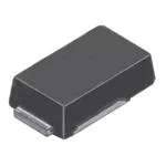
SMP (DO-220AA)
Anode
Cathode
TYPICAL APPLICATIONS
For general purpose regulation, industrial, and protection
applications.
LINKS TO ADDITIONAL RESOURCES
3D 3D
MECHANICAL DATA
3D Models
Case: SMP (DO-220AA)
Molding compound meets UL 94 V-0 flammability rating
Base P/N-M3 - halogen-free, RoHS-compliant, and
industrial grade
PRIMARY CHARACTERISTICS
VZ
5.6 V to 43 V
Ptot at TL = 75 °C
1500 mW
Ptot at TL = 25 °C
500 mW
TJ max.
150 °C
VZ specification
Pulse current
Package
SMP (DO-220AA)
Circuit configuration
Single
Terminals: matte tin plated leads, solderable
J-STD-002 and JESD 22-B102
M3 suffix meets JESD 201 class 1A whisker test
per
Polarity: color band denotes cathode end
PACKAGE
PACKAGE NAME
WEIGHT
SMP (DO-220AA)
24 mg
MOLDING COMPOUND MOISTURE SENSITIVITY
FLAMMABILITY RATING
LEVEL
MSL level 1
(according J-STD-020)
UL 94 V-0
SOLDERING
CONDITIONS
260 °C/10 s at terminals
MAXIMUM RATINGS (TA = 25 °C unless otherwise noted)
SYMBOL
VALUE
Power dissipation at TL = 75 °C (fig. 1) (1)
Ptot
1500
mW
Power dissipation at TA = 25 °C (fig. 1) (2)
Ptot
500
mW
Maximum instantaneous forward voltage at 200 mA for all types (3)
VF
1.5
V
TJ, TSTG
-65 to +150
°C
PARAMETER
Operating junction and storage temperature range
UNIT
Notes
(1) Mounted on PCB with 5.0 mm x 5.0 mm copper pads attached to each terminal
(2) Mounted on minimum recommended pad layout
(3) Pulse test: 300 μs pulse width, 1 % duty cycle
Revision: 25-Apr-2022
Document Number: 88482
1
For technical questions within your region: DiodesAmericas@vishay.com, DiodesAsia@vishay.com, DiodesEurope@vishay.com
THIS DOCUMENT IS SUBJECT TO CHANGE WITHOUT NOTICE. THE PRODUCTS DESCRIBED HEREIN AND THIS DOCUMENT
ARE SUBJECT TO SPECIFIC DISCLAIMERS, SET FORTH AT www.vishay.com/doc?91000
�SMPZ39XB thru SMPZ3940B
www.vishay.com
Vishay General Semiconductor
ELECTRICAL CHARACTERISTICS
SYMBOL
IF
PARAMETER
VZ
Reverse Zener voltage at IZT
IZT
Reverse current
ZZT
Maximum Zener impedance at IZT
IZK
Reverse current
ZZK
Maximum Zener impedance at IZK
IR
Reverse leakage current at VR
VR
Reverse voltage
IF
Forward current
VF
Forward voltage at IF
IZM
Maximum DC Zener current
VZ VR
V
IR VF
IZT
Zener Voltage Regulator
ELECTRICAL CHARACTERISTICS (TA = 25 °C unless otherwise noted)
PART
NUMBER
DEVICE
MARKING
CODE
ZENER VOLTAGE
RANGE
VZ at IZT
TEST CURRENT
IZT
V
SMPZ3919B
SMPZ3920B
SMPZ3921B
SMPZ3922B
SMPZ3923B
SMPZ3924B
SMPZ3925B
SMPZ3926B
SMPZ3927B
SMPZ3928B
SMPZ3929B
SMPZ3930B
SMPZ3931B
SMPZ3932B
SMPZ3933B
SMPZ3934B
SMPZ3935B
SMPZ3936B
SMPZ3937B
SMPZ3938B
SMPZ3939B
SMPZ3940B
19B
20B
21B
22B
23B
24B
25B
26B
27B
28B
29B
30B
31B
32B
33B
34B
35B
36B
37B
38B
39B
40B
MIN.
5.32
5.89
6.46
7.12
7.79
8.64
9.5
10.5
11.4
12.4
14.3
15.2
17.1
19.0
20.9
22.8
25.7
28.5
31.4
34.2
37.1
40.9
NOM.
5.6
6.2
6.8
7.5
8.2
9.1
10
11
12
13
15
16
18
20
22
24
27
30
33
36
39
43
IZK
MAXIMUM
ZENER
IMPEDANCE
ZZT AT IZT ZZK AT IZK
Ω
mA
MAX.
5.88
6.51
7.14
7.88
8.61
9.56
10.5
11.6
12.6
13.7
15.8
16.8
18.9
21
23.1
25.2
28.4
31.5
34.7
37.8
41
45.2
66.9
60.5
55.1
50.0
45.7
41.2
37.5
34.1
31.2
28.8
25
23.4
20.8
18.7
17.0
15.6
13.9
12.5
11.4
10.4
9.6
8.7
1.0
1.0
1.0
0.5
0.5
0.5
0.25
0.25
0.25
0.25
0.25
0.25
0.25
0.25
0.25
0.25
0.25
0.25
0.25
0.25
0.25
0.25
MAX.
5.0
2.0
2.5
3.0
3.5
4.0
4.5
5.5
6.5
7.0
9.0
10.0
12.0
14.0
17.5
19.0
23.0
26.0
33.0
38.0
45.0
53.0
MAX.
700
700
400
400
400
500
500
550
550
550
600
600
650
650
650
700
700
750
800
850
900
950
MAXIMUM
REVERSE
LEAKAGE
CURRENT
IR AT VR
MAXIMUM
ZENER
CURRENT
IZM
μA
V
mA
MAX.
200
200
200
150
50
10
2.5
0.5
0.5
0.5
0.5
0.5
0.5
0.5
0.5
0.5
0.5
0.5
0.5
0.5
0.5
0.5
3.0
4.0
5.2
6.0
6.5
7.0
8.0
8.4
9.1
9.9
11.4
12.2
13.7
15.2
16.7
18.2
20.6
22.8
25.1
27.4
29.7
32.7
MAX.
268
242
221
200
183
165
150
136
125
115
100
94
83
75
68
63
56
50
45
42
38
35
THERMAL CHARACTERISTICS (TA = 25 °C unless otherwise noted)
PARAMETER
SYMBOL
LIMIT
UNIT
Typical thermal resistance, junction to lead (1)
RθJL
50
°C/W
Typical thermal resistance, junction to ambient (2)
RθJA
250
°C/W
Notes
(1) Mounted on PCB with 5.0 mm x 5.0 mm copper pad areas attached to each terminal
(2) Mounted on minimum recommended pad layout
Revision: 25-Apr-2022
Document Number: 88482
2
For technical questions within your region: DiodesAmericas@vishay.com, DiodesAsia@vishay.com, DiodesEurope@vishay.com
THIS DOCUMENT IS SUBJECT TO CHANGE WITHOUT NOTICE. THE PRODUCTS DESCRIBED HEREIN AND THIS DOCUMENT
ARE SUBJECT TO SPECIFIC DISCLAIMERS, SET FORTH AT www.vishay.com/doc?91000
�SMPZ39XB thru SMPZ3940B
www.vishay.com
Vishay General Semiconductor
ORDERING INFORMATION (Example)
PREFERRED P/N
UNIT WEIGHT (g)
PREFERRED PACKAGE CODE
BASE QUANTITY
DELIVERY MODE
SMPZ3919B-M3/84A
0.024
84A
3000
7" diameter plastic tape and reel
SMPZ3919B-M3/85A
0.024
85A
10 000
13" diameter plastic tape and reel
4.0
100
3.5
IZ - Zener Test Current (mA)
Ptot - Maximum Power Dissipation (W)
RATINGS AND CHARACTERISTICS CURVES (TA = 25 °C unless otherwise noted)
3.0
2.5
2.0
TL
1.5
1.0
1
TA
0.5
0.1
0
0
25
50
75
100
125
0
150
20
40
60
Temperature (°C)
VZ - Zener Voltage (V)
Fig. 1 - Steady State Power Derating
Fig. 3 - Typical Zener Voltage
5.0
VZ - Temperature Coefficient (mV/°C)
100
IZ - Zener Test Current (mA)
10
10
1
0.1
VZ at IZT
4.0
3.0
2.0
1.0
0
0
1
2
3
4
5
6
7
8
9
10
5.0
5.5
6.0
6.5
VZ - Zener Voltage (V)
VZ - Zener Voltage (V)
Fig. 2 - Typical Zener Voltage
Fig. 4 - Typical temperature Coefficients
7.0
Revision: 25-Apr-2022
Document Number: 88482
3
For technical questions within your region: DiodesAmericas@vishay.com, DiodesAsia@vishay.com, DiodesEurope@vishay.com
THIS DOCUMENT IS SUBJECT TO CHANGE WITHOUT NOTICE. THE PRODUCTS DESCRIBED HEREIN AND THIS DOCUMENT
ARE SUBJECT TO SPECIFIC DISCLAIMERS, SET FORTH AT www.vishay.com/doc?91000
�SMPZ39XB thru SMPZ3940B
www.vishay.com
Vishay General Semiconductor
VZ - Temperature Coefficient (mV/°C)
50
VZ at IZT
40
30
20
10
0
0
20
10
30
40
50
VZ - Zener Voltage (V)
Fig. 5 - Typical Transient Temperature Coefficients
CJ - Junction Capacitance (pF)
10 000
Measured at Zero Bias
1000
Measured at VZ/2
100
10
10
0
100
VBR - Breakdown Voltage (V)
Fig. 6 - Typical Junction Capacitance
1000
ZZ - Dynamic Impedance (Ω)
IZ(rms) = 0.1 IZ(DC)
100
IZ = 1 mA
10
IZ = 10 mA
IZ = 20 mA
1
10
15
20
25
30
35
40
45
VZ - Zener Voltage (V)
Fig. 7 - Typical Zener Impedance
Revision: 25-Apr-2022
Document Number: 88482
4
For technical questions within your region: DiodesAmericas@vishay.com, DiodesAsia@vishay.com, DiodesEurope@vishay.com
THIS DOCUMENT IS SUBJECT TO CHANGE WITHOUT NOTICE. THE PRODUCTS DESCRIBED HEREIN AND THIS DOCUMENT
ARE SUBJECT TO SPECIFIC DISCLAIMERS, SET FORTH AT www.vishay.com/doc?91000
�SMPZ39XB thru SMPZ3940B
www.vishay.com
Vishay General Semiconductor
PACKAGE OUTLINE DIMENSIONS in inches (millimeters)
SMP (DO-220AA)
0.012 (0.30) REF.
Cathode Band
0.053 (1.35)
0.041 (1.05)
0.086 (2.18)
0.074 (1.88)
0.142 (3.61)
0.126 (3.19)
0.036 (0.91)
0.024 (0.61)
0.032 (0.80)
0.016 (0.40)
0.103 (2.60)
0.087 (2.20)
0.158 (4.00)
0.146 (3.70)
Mounting pad layout
0.105
(2.67)
0.013 (0.35)
0.004 (0.10)
0.025 0.030
(0.635) (0.762)
0.045 (1.15)
0.033 (0.85)
0.012 (0.30) 0.018 (0.45)
0.000 (0.00) 0.006 (0.15)
0.100
(2.54)
0.050
(1.27)
Revision: 25-Apr-2022
Document Number: 88482
5
For technical questions within your region: DiodesAmericas@vishay.com, DiodesAsia@vishay.com, DiodesEurope@vishay.com
THIS DOCUMENT IS SUBJECT TO CHANGE WITHOUT NOTICE. THE PRODUCTS DESCRIBED HEREIN AND THIS DOCUMENT
ARE SUBJECT TO SPECIFIC DISCLAIMERS, SET FORTH AT www.vishay.com/doc?91000
�Legal Disclaimer Notice
www.vishay.com
Vishay
Disclaimer
ALL PRODUCT, PRODUCT SPECIFICATIONS AND DATA ARE SUBJECT TO CHANGE WITHOUT NOTICE TO IMPROVE
RELIABILITY, FUNCTION OR DESIGN OR OTHERWISE.
Vishay Intertechnology, Inc., its affiliates, agents, and employees, and all persons acting on its or their behalf (collectively,
“Vishay”), disclaim any and all liability for any errors, inaccuracies or incompleteness contained in any datasheet or in any other
disclosure relating to any product.
Vishay makes no warranty, representation or guarantee regarding the suitability of the products for any particular purpose or
the continuing production of any product. To the maximum extent permitted by applicable law, Vishay disclaims (i) any and all
liability arising out of the application or use of any product, (ii) any and all liability, including without limitation special,
consequential or incidental damages, and (iii) any and all implied warranties, including warranties of fitness for particular
purpose, non-infringement and merchantability.
Statements regarding the suitability of products for certain types of applications are based on Vishay's knowledge of typical
requirements that are often placed on Vishay products in generic applications. Such statements are not binding statements
about the suitability of products for a particular application. It is the customer's responsibility to validate that a particular product
with the properties described in the product specification is suitable for use in a particular application. Parameters provided in
datasheets and / or specifications may vary in different applications and performance may vary over time. All operating
parameters, including typical parameters, must be validated for each customer application by the customer's technical experts.
Product specifications do not expand or otherwise modify Vishay's terms and conditions of purchase, including but not limited
to the warranty expressed therein.
Hyperlinks included in this datasheet may direct users to third-party websites. These links are provided as a convenience and
for informational purposes only. Inclusion of these hyperlinks does not constitute an endorsement or an approval by Vishay of
any of the products, services or opinions of the corporation, organization or individual associated with the third-party website.
Vishay disclaims any and all liability and bears no responsibility for the accuracy, legality or content of the third-party website
or for that of subsequent links.
Except as expressly indicated in writing, Vishay products are not designed for use in medical, life-saving, or life-sustaining
applications or for any other application in which the failure of the Vishay product could result in personal injury or death.
Customers using or selling Vishay products not expressly indicated for use in such applications do so at their own risk. Please
contact authorized Vishay personnel to obtain written terms and conditions regarding products designed for such applications.
No license, express or implied, by estoppel or otherwise, to any intellectual property rights is granted by this document or by
any conduct of Vishay. Product names and markings noted herein may be trademarks of their respective owners.
© 2022 VISHAY INTERTECHNOLOGY, INC. ALL RIGHTS RESERVED
Revision: 01-Jan-2022
1
Document Number: 91000
�


 工商网监
湘ICP备2023018690号
工商网监
湘ICP备2023018690号
