V3FL45
www.vishay.com
Vishay General Semiconductor
Surface-Mount TMBS® (Trench MOS Barrier Schottky) Rectifiers
FEATURES
eSMP®
Series
• Trench MOS Schottky technology
Available
• Low profile package
• Ideal for automated placement
• Low forward voltage drop, low power losses
Top view
Bottom view
J-STD-020,
• Wave and reflow solderable
SMF (DO-219AB)
Cathode
• Meets MSL level 1, per
LF maximum peak of 260 °C
Anode
• AEC-Q101 qualified available
- Automotive ordering code: base P/NHM3
• Compatible to SOD-123W package case outline
LINKS TO ADDITIONAL RESOURCES
3D 3D
3D Models
• Material categorization: for definitions of compliance
please see www.vishay.com/doc?99912
TYPICAL APPLICATIONS
PRIMARY CHARACTERISTICS
IF(AV)
3.0 A
VRRM
45 V
IFSM
50 A
VF at IF = 2 A (TA = 125 °C)
0.43 V
TJ max.
150 °C
Package
SMF (DO-219AB)
Circuit configuration
Single
For use in high frequency inverters, freewheeling, DC/DC
converters, and polarity protection in commercial, industrial,
and automotive applications.
MECHANICAL DATA
Case: SMF (DO-219AB)
Molding compound meets UL 94 V-0 flammability rating
Base P/N-M3 - halogen-free, RoHS-compliant
Base P/NHM3 - halogen-free, RoHS-compliant, and
AEC-Q101 qualified
Terminals: matte tin plated leads, solderable per
J-STD-002 and JESD 22-B102
M3 and HM3 suffix meet JESD 201 class 2 whisker test
Polarity: color band denotes the cathode end
MAXIMUM RATINGS (TA = 25 °C unless otherwise noted)
PARAMETER
SYMBOL
Device marking code
Maximum repetitive peak reverse voltage
V3FL45
VRRM
45
IF(AV) (1)
2.5
IF(AV) (2)
3.0
IFSM
50
Operating junction temperature range
TJ (3)
-40 to +150
Storage temperature range
TSTG
-55 to +150
Maximum average forward rectified current (fig.1)
Peak forward surge current 8.3 ms single half sine-wave superimposed
on rated load
UNIT
3LE
V
A
A
°C
Notes
(1) Free air, mounted on FR4 PCB, 2 oz. standard footprint
(2) Mounted on FR4 PCB, 2 oz.10 mm x 10 mm copper pad area
(3) The heat generated must be less than the thermal conductivity from junction-to-ambient: dP /dT < 1/R
D
J
θJA
Revision: 13-May-2020
Document Number: 87568
1
For technical questions within your region: DiodesAmericas@vishay.com, DiodesAsia@vishay.com, DiodesEurope@vishay.com
THIS DOCUMENT IS SUBJECT TO CHANGE WITHOUT NOTICE. THE PRODUCTS DESCRIBED HEREIN AND THIS DOCUMENT
ARE SUBJECT TO SPECIFIC DISCLAIMERS, SET FORTH AT www.vishay.com/doc?91000
�V3FL45
www.vishay.com
Vishay General Semiconductor
ELECTRICAL CHARACTERISTICS (TA = 25 °C unless otherwise noted)
PARAMETER
TEST CONDITIONS
IF = 1.5 A
Instantaneous forward voltage
TA = 25 °C
IF = 3.0 A
VF (1)
IF = 1.5 A
TA = 125 °C
IF = 3.0 A
Reverse current
VR = 45 V
Typical junction capacitance
4.0 V, 1 MHz
SYMBOL
TA = 25 °C
TYP.
MAX.
0.44
-
0.50
0.58
0.34
-
0.43
0.51
-
0.75
4
15
370
-
IR (2)
TA = 125 °C
CJ
UNIT
V
mA
pF
Notes
(1) Pulse test: 300 μs pulse width, 1 % duty cycle
(2) Pulse test: Pulse width ≤ 5 ms
THERMAL CHARACTERISTICS (TA = 25 °c unless otherwise noted)
PARAMETER
SYMBOL
RθJA
Typical thermal resistance
V3FL45
(1)(2)
UNIT
125
RθJM (3)
°C/W
18
Notes
(1) The heat generated must be less than the thermal conductivity from junction-to-ambient: dP /dT
很抱歉,暂时无法提供与“V3FL45-M3/I”相匹配的价格&库存,您可以联系我们找货
免费人工找货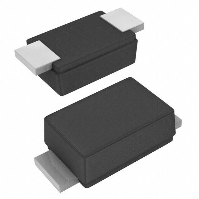


 工商网监
湘ICP备2023018690号
工商网监
湘ICP备2023018690号
