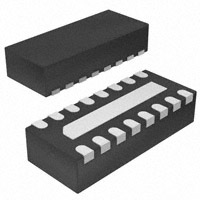
VEMI85AB-HGK
www.vishay.com
Vishay Semiconductors
8-Channel EMI-Filter with ESD-Protection
FEATURES
• Ultra compact LLP3313-17L package
• Low package profile of 0.6 mm
• 8-channel EMI-filter
• Low leakage current
• Line resistance RS = 100
• Typical cut off frequency f3dB = 130 MHz
21840
16
14
15
13
11
12
10
• ESD-protection acc. IEC 61000-4-2
± 18 kV contact discharge
± 25 kV air discharge
9
• e4 - precious metal (e.g. Ag, Au, NiPd, NiPdAu) (no Sn)
17
• Material categorization: for definitions of compliance
please see www.vishay.com/doc?99912
20388
1
3
2
4
7
6
5
8
MARKING (example only)
YYXX
20720
Dot = pin 1 marking
Y = type code (see table below)
XX = date code
DESIGN SUPPORT TOOLS
click logo to get started
Models
Available
ORDERING INFORMATION
DEVICE NAME
ORDERING CODE
TAPED UNITS PER REEL
(8 mm TAPE ON 7" REEL)
MINIMUM ORDER QUANTITY
VEMI85AB-HGK
VEMI85AB-HGK-GS08
3000
15 000
PACKAGE DATA
DEVICE NAME
PACKAGE
NAME
VEMI85AB-HGK
LLP3313-17L
TYPE
MOLDING COMPOUND
WEIGHT
CODE
FLAMMABILITY RATING
9U
7.4 mg
UL 94 V-0
MOISTURE
SENSITIVITY LEVEL
SOLDERING CONDITIONS
MSL level 1
(according J-STD-020)
Peak temperature max. 260 °C
ABSOLUTE MAXIMUM RATINGS
PARAMETER
Peak pulse current
ESD immunity
Operating temperature
Storage temperature
Rev. 1.6, 09-Jan-2019
TEST CONDITIONS
SYMBOL
VALUE
UNIT
All I/O pin to pin 17; acc. IEC 61000-4-5;
tp = 8/20 μs; single shot
IPPM
4
A
Contact discharge acc. IEC 61000-4-2; 10 pulses
Air discharge acc. IEC 61000-4-2; 10 pulses
Junction temperature
VESD
± 18
± 25
kV
TJ
-40 to +125
°C
TSTG
-55 to +150
°C
Document Number: 81718
1
For technical questions, contact: EMIfilter@vishay.com
THIS DOCUMENT IS SUBJECT TO CHANGE WITHOUT NOTICE. THE PRODUCTS DESCRIBED HEREIN AND THIS DOCUMENT
ARE SUBJECT TO SPECIFIC DISCLAIMERS, SET FORTH AT www.vishay.com/doc?91000
�VEMI85AB-HGK
www.vishay.com
Vishay Semiconductors
APPLICATION NOTE
With the VEMI85AB-HGK 8 different signal or data lines can be filtered and clamped to ground. Due to the different clamping
levels in forward and reverse direction the clamping behaviour is Bidirectional and Asymmetric (BiAs).
L1OUT
L1IN
1
16
L2IN
2
15
L2OUT
14
L3OUT
L3IN
3
17
13
L4OUT
5
12
L5OUT
6
11
L6OUT
L7IN
7
10
L7OUT
L8IN
8
9
L8OUT
L4IN
L5IN
L6IN
4
20389
The 8 independent EMI-filter are placed between
pin 1 and pin 16,
pin 2 and pin 15,
pin 3 and pin 14,
pin 4 and pin 13,
pin 5 and pin 12,
pin 6 and pin 11,
pin 7 and pin 10 and
pin 8 and pin 9.
They all are connected to a common ground pin 17 on the backside of the package.
The circuit diagram of one EMI-filter-channel shows two identical Z-diodes at the input to ground and the output to ground.
These Z-diodes are characterized by the breakthrough voltage level (VBR) and the diode capacitance (CD). Below the
breakthrough voltage level the Z-diodes can be considered as capacitors. Together with these capacitors and the line
resistance RS between input and output the device works as a low pass filter. Low frequency signals (f < f3dB) pass the filter
while high frequency signals (f > f3dB) will be shorted to ground through the diode capacitances CD.
RS
In
(pin 1, 2, 3, 4, 5, 6, 7, 8)
Out
(pin 9, 10, 11, 12, 13, 14, 15, 16)
CD
20390
CD
GND
(pin 17)
Each filter is symmetrical so that both ports can be used as input or output.
Rev. 1.6, 09-Jan-2019
Document Number: 81718
2
For technical questions, contact: EMIfilter@vishay.com
THIS DOCUMENT IS SUBJECT TO CHANGE WITHOUT NOTICE. THE PRODUCTS DESCRIBED HEREIN AND THIS DOCUMENT
ARE SUBJECT TO SPECIFIC DISCLAIMERS, SET FORTH AT www.vishay.com/doc?91000
�VEMI85AB-HGK
www.vishay.com
Vishay Semiconductors
ELECTRICAL CHARACTERISTICS All inputs (pin 1, 2, 3, 4, 5, 6, 7, and 8) to ground (pin 17)
(Tamb = 25 °C, unless otherwise specified)
PARAMETER
TEST CONDITIONS/REMARKS
SYMBOL
MIN.
TYP.
MAX.
UNIT
Number of channels which can be protected
Nchannel
-
-
8
channel
Max. reverse working voltage
VRWM
-
-
5
V
Reverse voltage
at IR = 1 μA
VR
5
-
-
V
Reverse current
at VR = VRWM
IR
-
0.25
1
μA
Reverse break down voltage
at IR = 1 mA
VBR
6
6.8
-
V
at IPP = 1 A applied at the input,
measured at the output; acc. IEC 61000-4-5
VC-out
-
-
7
V
at IPP = IPPM = 4 A applied at the input,
measured at the output; acc. IEC 61000-4-5
VC-out
-
-
8
V
at IPP = -1 A applied at the input,
measured at the output; acc. IEC 61000-4-5
VC-out
-1.4
-
-
V
at IPP = IPPM = -4 A applied at the input,
measured at the output; acc. IEC 61000-4-5
VC-out
-1.6
-
-
V
at VR = 0 V; f = 1 MHz
CIN
-
40
45
pF
at VR = 2.5 V; f = 1 MHz
CIN
-
24
28
pF
at ± 18 kV ESD-pulse acc. IEC 61000-4-2
VCESD
-
7.5
-
V
Line resistance
Measured between input and output;
IS = 10 mA
RS
90
100
110
Cut-off frequency
VIN = 0 V; measured in a 50 system
f3dB
-
130
-
MHz
Protection paths
Reverse stand off voltage
Pos. clamping voltage
Neg. clamping voltage
Input capacitance
ESD-clamping voltage
TYPICAL CHARACTERISTICS (Tamb = 25 °C, unless otherwise specified)
120 %
Rise time = 0.7 ns to 1 ns
8 µs to 100 %
100 %
80 %
80 %
60 %
60 %
IPPM
Discharge Current IESD
100 %
53 %
40 %
27 %
20 %
20 %
0%
-10 0 10 20 30 40 50 60 70 80 90 100
Time (ns)
20557
Fig. 1 - ESD Discharge Current Wave Form
acc. IEC 61000-4-2 (330 /150 pF)
Rev. 1.6, 09-Jan-2019
20 µs to 50 %
40 %
0%
0
20548
10
20
30
40
Time (µs)
Fig. 2 - 8/20 μs Peak Pulse Current Wave Form
acc. IEC 61000-4-5
Document Number: 81718
3
For technical questions, contact: EMIfilter@vishay.com
THIS DOCUMENT IS SUBJECT TO CHANGE WITHOUT NOTICE. THE PRODUCTS DESCRIBED HEREIN AND THIS DOCUMENT
ARE SUBJECT TO SPECIFIC DISCLAIMERS, SET FORTH AT www.vishay.com/doc?91000
�VEMI85AB-HGK
www.vishay.com
Vishay Semiconductors
45
100
f = 1 MHz
40
10
35
30
CIN (pF)
IF (mA)
1
0.1
25
20
15
10
0.01
5
0
0.001
0.5
0.6
0.7
20726
0.8
0.9
0
1
VF (V)
Fig. 3 - Typical Forward Current IF vs. Forward Voltage VF
2
3
4
5
6
VIN (V)
Fig. 6 - Typical Input Capacitance CIN vs. Input Voltage VIN
0
Transmission (S21) in dB
8
7
6
5
VR (V)
1
20725
4
3
2
-5
- 10
- 40
1
10
100
20724
Fig. 4 - Typical Reverse Voltage VR vs.
Reverse Current IR
Measured in a 50 Ω system
1
1000 10 000
IR (µA)
VINPUT = 0 V
- 30
- 35
0.1
VINPUT = 1 V
- 25
0
0.01
VINPUT = 2 V
- 20
1
20727
VINPUT = 5 V
- 15
10
100
1000
10 000
Frequency in MHz
Fig. 7 - Typical Small Signal Transmission (S21)
at ZO = 50
12
Input clamping voltage
10
VC (V)
8
Output clamping voltage
6
4
Measured
acc. IEC 61000-4-5
(8/20 µs - wave form)
2
VC
0
0
20728
1
2
3
4
5
IPP (A)
Fig. 5 - Typical Peak Clamping Voltage VC vs.
Peak Pulse Current IPP
Rev. 1.6, 09-Jan-2019
Document Number: 81718
4
For technical questions, contact: EMIfilter@vishay.com
THIS DOCUMENT IS SUBJECT TO CHANGE WITHOUT NOTICE. THE PRODUCTS DESCRIBED HEREIN AND THIS DOCUMENT
ARE SUBJECT TO SPECIFIC DISCLAIMERS, SET FORTH AT www.vishay.com/doc?91000
�VEMI85AB-HGK
www.vishay.com
Vishay Semiconductors
PACKAGE DIMENSIONS in millimeters (inches): LLP3313-17L
2.65 (0.104)
2.55 (0.100) exp. DAP
0.23 (0.009)
0.4 (0.016) bsc
0.3 (0.012)
0.24 (0.009)
exp. DAP
0.45 (0.018)
0.35 (0.014)
0.2 (0.008) x 45°
0.17 (0.007)
2.8 (0.110) ref.
1.4 (0.055)
0.5 (0.020)
3.35 (0.132)
3.25 (0.128)
0.6 (0.024)
0.152 (0.006) ref.
0 (0.000)
0.05 (0.002)
1.3 (0.051)
Pin 1 marking
Foot print recommendation:
7 x 0.4 = 2.8 (0.110)
0.4 (0.016)
Solder
resist mask
0.42 (0.017)
Document no.:S8-V-3906.04-003 (4)
Created - Date: 28. August 2006
Rev. 1 - Date: 27. May 2008
0.4 (0.016)
2.6 (0.102)
0.4 (0.016)
0.15 (0.006)
0.2 (0.008)
Solder pad
20391
Rev. 1.6, 09-Jan-2019
Document Number: 81718
5
For technical questions, contact: EMIfilter@vishay.com
THIS DOCUMENT IS SUBJECT TO CHANGE WITHOUT NOTICE. THE PRODUCTS DESCRIBED HEREIN AND THIS DOCUMENT
ARE SUBJECT TO SPECIFIC DISCLAIMERS, SET FORTH AT www.vishay.com/doc?91000
�Legal Disclaimer Notice
www.vishay.com
Vishay
Disclaimer
ALL PRODUCT, PRODUCT SPECIFICATIONS AND DATA ARE SUBJECT TO CHANGE WITHOUT NOTICE TO IMPROVE
RELIABILITY, FUNCTION OR DESIGN OR OTHERWISE.
Vishay Intertechnology, Inc., its affiliates, agents, and employees, and all persons acting on its or their behalf (collectively,
“Vishay”), disclaim any and all liability for any errors, inaccuracies or incompleteness contained in any datasheet or in any other
disclosure relating to any product.
Vishay makes no warranty, representation or guarantee regarding the suitability of the products for any particular purpose or
the continuing production of any product. To the maximum extent permitted by applicable law, Vishay disclaims (i) any and all
liability arising out of the application or use of any product, (ii) any and all liability, including without limitation special,
consequential or incidental damages, and (iii) any and all implied warranties, including warranties of fitness for particular
purpose, non-infringement and merchantability.
Statements regarding the suitability of products for certain types of applications are based on Vishay's knowledge of typical
requirements that are often placed on Vishay products in generic applications. Such statements are not binding statements
about the suitability of products for a particular application. It is the customer's responsibility to validate that a particular product
with the properties described in the product specification is suitable for use in a particular application. Parameters provided in
datasheets and / or specifications may vary in different applications and performance may vary over time. All operating
parameters, including typical parameters, must be validated for each customer application by the customer's technical experts.
Product specifications do not expand or otherwise modify Vishay's terms and conditions of purchase, including but not limited
to the warranty expressed therein.
Hyperlinks included in this datasheet may direct users to third-party websites. These links are provided as a convenience and
for informational purposes only. Inclusion of these hyperlinks does not constitute an endorsement or an approval by Vishay of
any of the products, services or opinions of the corporation, organization or individual associated with the third-party website.
Vishay disclaims any and all liability and bears no responsibility for the accuracy, legality or content of the third-party website
or for that of subsequent links.
Except as expressly indicated in writing, Vishay products are not designed for use in medical, life-saving, or life-sustaining
applications or for any other application in which the failure of the Vishay product could result in personal injury or death.
Customers using or selling Vishay products not expressly indicated for use in such applications do so at their own risk. Please
contact authorized Vishay personnel to obtain written terms and conditions regarding products designed for such applications.
No license, express or implied, by estoppel or otherwise, to any intellectual property rights is granted by this document or by
any conduct of Vishay. Product names and markings noted herein may be trademarks of their respective owners.
© 2022 VISHAY INTERTECHNOLOGY, INC. ALL RIGHTS RESERVED
Revision: 01-Jan-2022
1
Document Number: 91000
�


 工商网监
湘ICP备2023018690号
工商网监
湘ICP备2023018690号
