VS-25TTS08FP-M3, VS-25TTS12FP-M3
www.vishay.com
Vishay Semiconductors
Thyristor High Voltage, Phase Control SCR, 25 A
2
(A)
FEATURES
• Designed and qualified for industrial level
• Fully isolated package (VINS = 2500 VRMS)
• UL pending
• 125 °C max. operating junction temperature
1
2
3
1 (K) (G) 3
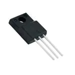
3L TO-220 FullPAK
• Material categorization: for definitions of compliance
please see www.vishay.com/doc?99912
APPLICATIONS
PRIMARY CHARACTERISTICS
IT(AV)
16 A
VDRM/VRRM
800 V, 1200 V
• Typical usage is in input rectification crowbar (soft start)
and AC switch in motor control, UPS, welding, and battery
charge
VTM
1.25 V
DESCRIPTION
IGT
45 mA
TJ
-40 °C to 125 °C
Package
3L TO-220 FullPAK
Circuit configuration
Single SCR
The VS-25TTS...FP... high voltage series of silicon
controlled rectifiers are specifically designed for medium
power switching and phase control applications. The glass
passivation technology used has reliable operation up to
125 °C junction temperature.
OUTPUT CURRENT IN TYPICAL APPLICATIONS
APPLICATIONS
Capacitive input filter TA = 55 °C,
TJ = 125 °C, common heatsink
of 1 °C/W
SINGLE-PHASE BRIDGE
THREE-PHASE BRIDGE
UNITS
18
22
A
VALUES
UNITS
MAJOR RATINGS AND CHARACTERISTICS
PARAMETER
IT(AV)
TEST CONDITIONS
Sinusoidal waveform
25
IRMS
VRRM/VDRM
ITSM
VT
16
16 A, TJ = 25 °C
A
800, 1200
V
350
A
1.25
V
dV/dt
500
V/μs
dI/dt
150
A/μs
-40 to +125
°C
VRRM, MAXIMUM PEAK
REVERSE VOLTAGE
V
VDRM, MAXIMUM PEAK
DIRECT VOLTAGE
V
IRRM/IDRM
AT 125 °C
mA
VS-25TTS08FP-M3
800
800
VS-25TTS12FP-M3
1200
1200
TJ
VOLTAGE RATINGS
PART NUMBER
10
Revision: 09-Jan-18
Document Number: 96300
1
For technical questions within your region: DiodesAmericas@vishay.com, DiodesAsia@vishay.com, DiodesEurope@vishay.com
THIS DOCUMENT IS SUBJECT TO CHANGE WITHOUT NOTICE. THE PRODUCTS DESCRIBED HEREIN AND THIS DOCUMENT
ARE SUBJECT TO SPECIFIC DISCLAIMERS, SET FORTH AT www.vishay.com/doc?91000
�VS-25TTS08FP-M3, VS-25TTS12FP-M3
www.vishay.com
Vishay Semiconductors
ABSOLUTE MAXIMUM RATINGS
PARAMETER
SYMBOL
Maximum average on-state current
IT(AV)
Maximum RMS on-state current
IRMS
Maximum peak, one-cycle,
non-repetitive surge current
ITSM
TEST CONDITIONS
VALUES
TYP. MAX.
TC = 51 °C, 180° conduction half sine wave
UNITS
16
25
10 ms sine pulse, rated VRRM applied
300
10 ms sine pulse, no voltage reapplied
350
10 ms sine pulse, rated VRRM applied
450
10 ms sine pulse, no voltage reapplied
630
A
Maximum I2t for fusing
I2t
Maximum I2t for fusing
I2t
t = 0.1ms to 10 ms, no voltage reapplied
6300
A2s
Maximum on-state voltage drop
VTM
16 A, TJ = 25 °C
1.25
V
12.0
m
1.0
V
On-state slope resistance
Threshold voltage
Maximum reverse and direct leakage current
rt
VT(TO)
IRM/IDM
TJ = 125 °C
TJ = 25 °C
TJ = 125 °C
A2s
0.5
VR = Rated VRRM/VDRM
10
Holding current
IH
Anode supply = 6 V, resistive load, initial IT = 1 A,
TJ = 25 °C
Maximum latching current
IL
Anode supply = 6 V, resistive load, TJ = 25 °C
200
TJ = TJ max., linear to 80 %, VDRM = Rg - k = Open
500
V/μs
150
A/μs
VALUES
UNITS
Maximum rate of rise of off-state voltage
dV/dt
Maximum rate of rise of turned-on current
dI/dt
150
-
mA
TRIGGERING
PARAMETER
TEST CONDITIONS
SYMBOL
PGM
8.0
Maximum average gate power
PG(AV)
2.0
Maximum peak positive gate current
+ IGM
1.5
A
Maximum peak negative gate voltage
- VGM
10
V
Maximum peak gate power
Maximum required DC gate current to trigger
IGT
Maximum required DC gate
voltage to trigger
VGT
Maximum DC gate voltage not to trigger
VGD
Maximum DC gate current not to trigger
IGD
Anode supply = 6 V, resistive load, TJ = - 10 °C
60
Anode supply = 6 V, resistive load, TJ = 25 °C
45
Anode supply = 6 V, resistive load, TJ = 125 °C
20
Anode supply = 6 V, resistive load, TJ = - 10 °C
2.5
Anode supply = 6 V, resistive load, TJ = 25 °C
2.0
Anode supply = 6 V, resistive load, TJ = 125 °C
1.0
TJ = 125 °C, VDRM = Rated value
W
mA
V
0.25
2.0
mA
VALUES
UNITS
SWITCHING
PARAMETER
SYMBOL
Typical turn-on time
tgt
Typical reverse recovery time
trr
Typical turn-off time
tq
TEST CONDITIONS
TJ = 25 °C
TJ = 125 °C
0.9
4
µs
110
Revision: 09-Jan-18
Document Number: 96300
2
For technical questions within your region: DiodesAmericas@vishay.com, DiodesAsia@vishay.com, DiodesEurope@vishay.com
THIS DOCUMENT IS SUBJECT TO CHANGE WITHOUT NOTICE. THE PRODUCTS DESCRIBED HEREIN AND THIS DOCUMENT
ARE SUBJECT TO SPECIFIC DISCLAIMERS, SET FORTH AT www.vishay.com/doc?91000
�VS-25TTS08FP-M3, VS-25TTS12FP-M3
www.vishay.com
Vishay Semiconductors
THERMAL AND MECHANICAL SPECIFICATIONS
PARAMETER
SYMBOL
Maximum junction and storage
temperature range
TJ, TStg
Maximum thermal resistance,
junction to case
RthJC
Maximum thermal resistance,
junction to ambient
RthJA
Typical thermal resistance,
case to heatsink
RthCS
TEST CONDITIONS
DC operation
Mounting surface, smooth, and greased
0.5
0.07
oz.
maximum
12 (10)
kgf · cm
(lbf · in)
100
80
60
60° 90°
120°
20
180°
0
5
10
15
20
Average On-State Current (A)
Maximum Average On-state Power Loss (W)
Maximum Allowable Case Temperature (°C)
120
30°
140
120
100
80
60
60°
90°
120°
180°
DC
0
5
10
15
20
25
Average On-state Current (A)
Fig. 2 - Current Rating Characteristics
25TTS12FP
180°
120°
90°
60°
30°
20
15
RMS Limit
10
Conduction Angle
5
TJ = 125 °C
0
0
4
8
12
16
20
Average On-state Current (A)
Fig. 3 - On-State Power Loss Characteristics
30
Maximum Average On-state Power Loss (W)
Maximum Allowable Case Temperature (°C)
25TTS08FP
25
Fig. 1 - Current Rating Characteristics
20
g
6 (5)
140
0
°C/W
62
Case style 3L TO-220 FullPAK
30°
°C
minimum
Marking device
40
-40 to 125
2
Mounting torque
0
UNITS
2.5
Approximate weight
40
VALUES
35
DC
180°
120°
90°
60°
30°
30
25
20
RMS Limit
15
Conduction Period
10
TJ = 125 °C
5
0
0
5
10
15
20
25
30
Average On-state Current (A)
Fig. 4 - On-State Power Loss Characteristics
Revision: 09-Jan-18
Document Number: 96300
3
For technical questions within your region: DiodesAmericas@vishay.com, DiodesAsia@vishay.com, DiodesEurope@vishay.com
THIS DOCUMENT IS SUBJECT TO CHANGE WITHOUT NOTICE. THE PRODUCTS DESCRIBED HEREIN AND THIS DOCUMENT
ARE SUBJECT TO SPECIFIC DISCLAIMERS, SET FORTH AT www.vishay.com/doc?91000
�VS-25TTS08FP-M3, VS-25TTS12FP-M3
350
Vishay Semiconductors
Peak Half Sine Wave On-state Current (A)
Peak Half Sine Wave On-state Current (A)
www.vishay.com
At any rated load condition and with
Rated V RRM applied following surge.
Initial TJ = 125 °C
at 60 Hz 0.0083 s
at 50 Hz 0.0100 s
300
250
200
150
1
10
100
400
Maximum non repetitive surge current
vs. pulse train duration.
Control of conduction may not be maintained.
Initial TJ = 125 °C
No voltage reapplied
Rated VRRM reapplied
350
300
250
200
150
100
0.01
Number Of Equal Amplitude Half Cycle
Current Pulses (N)
0.1
1
Pulse Train Duration (s)
Fig. 5 - Maximum Non-Repetitive Surge Current
Fig. 6 - Maximum Non-Repetitive Surge Current
Instantaneous On-state Current (A)
1000
100
TJ = 25 °C
TJ = 125 °C
10
1
0
1
2
3
4
5
Instantaneous On-state Voltage (V)
Fig. 7 - On-State Voltage Drop Characteristics
Thermal Impedance ZthJC (°C/W)
10
D = 0.5
D = 0.2
1
D = 0.1
D = 0.05
D = 0.02
D = 0.01
0.1
0.01
1E-05
Single Pulse
(Thermal Resistance)
1E-04
1E-03
1E-02
1E-01
1E+00
1E+01
1E+02
Square Wave Pulse Duration (s)
Fig. 8 - Thermal Impedance ZthJC Characteristics
Revision: 09-Jan-18
Document Number: 96300
4
For technical questions within your region: DiodesAmericas@vishay.com, DiodesAsia@vishay.com, DiodesEurope@vishay.com
THIS DOCUMENT IS SUBJECT TO CHANGE WITHOUT NOTICE. THE PRODUCTS DESCRIBED HEREIN AND THIS DOCUMENT
ARE SUBJECT TO SPECIFIC DISCLAIMERS, SET FORTH AT www.vishay.com/doc?91000
�VS-25TTS08FP-M3, VS-25TTS12FP-M3
www.vishay.com
Vishay Semiconductors
Rectangular gate pulse
a)Recommended load line for
rated di/ dt: 10 V, 20 ohms
tr = 0.5 µs, tp >= 6 µs
b)Rec ommended load line for
= 6 µs
(1) PGM = 40 W, tp = 1 ms
(2) PGM = 20 W, tp = 2 ms
(3) PGM = 8 W, tp = 5 ms
(4) PGM = 4 W, tp = 10 ms
(a)
(b)
1
VGD
TJ = -10 °C
TJ = 125 °C
TJ = 25 °C
Instantaneous Gate Voltage (V)
100
(3)
(4)
IGD
(2)
(1)
Frequenc y Limited by PG(AV)
0.1
0.001
0.01
0.1
1
10
100
Instantaneous Gate Current (A)
Fig. 9 - Gate Characteristics
ORDERING INFORMATION TABLE
Device code
VS-
25
T
T
S
12
FP
-M3
1
2
3
4
5
6
7
8
1
-
Vishay Semiconductors product
2
-
Current rating (25 = 25 A)
3
-
Circuit configuration:
4
-
Package:
T = single thyristor
T = TO-220AB
5
-
Type of silicon:
6
-
Voltage code x 100 = VRRM
7
-
FullPAK
8
-
Environmental digit:
Standard recovery rectifier
08 = 800 V
12 = 1200 V
-M3 = halogen-free, RoHS-compliant, and terminations lead (Pb)-free
ORDERING INFORMATION (Example)
PREFERRED P/N
QUANTITY PER T/R
MINIMUM ORDER QUANTITY
PACKAGING DESCRIPTION
VS-25TTS08FP-M3
50
1000
Antistatic plastic tubes
VS-25TTS12FP-M3
50
1000
Antistatic plastic tubes
LINKS TO RELATED DOCUMENTS
Dimensions
www.vishay.com/doc?96155
Part marking information
www.vishay.com/doc?95456
Revision: 09-Jan-18
Document Number: 96300
5
For technical questions within your region: DiodesAmericas@vishay.com, DiodesAsia@vishay.com, DiodesEurope@vishay.com
THIS DOCUMENT IS SUBJECT TO CHANGE WITHOUT NOTICE. THE PRODUCTS DESCRIBED HEREIN AND THIS DOCUMENT
ARE SUBJECT TO SPECIFIC DISCLAIMERS, SET FORTH AT www.vishay.com/doc?91000
�Outline Dimensions
www.vishay.com
Vishay Semiconductors
3L TO-220 FullPAK
DIMENSIONS in millimeters
3.40
Hole Ø 3.10
10.6
10.0
3.7
3.2
2.80
2.44
7.31
6.50
16.0
15.8
Mold flash bleeding
3.3
3.1
Exposed Cu
13.56
12.90
2.54 TYP.
0.61
0.38
0.9
0.7
2.85
2.65
2.54 TYP.
1.20
1.47
1.30
1.05
Bottom view
R 0.7
(2 places)
R 0.5
4.8
4.6
5° ± 0.5°
5° ± 0.5°
Notes
(1) All dimensions are in mm
(2) Package body size exclude mold flash and burrs. Moldflash should be less than 6 mils
Revision: 06-Jul-17
Document Number: 96155
1
For technical questions within your region: DiodesAmericas@vishay.com, DiodesAsia@vishay.com, DiodesEurope@vishay.com
THIS DOCUMENT IS SUBJECT TO CHANGE WITHOUT NOTICE. THE PRODUCTS DESCRIBED HEREIN AND THIS DOCUMENT
ARE SUBJECT TO SPECIFIC DISCLAIMERS, SET FORTH AT www.vishay.com/doc?91000
�Legal Disclaimer Notice
www.vishay.com
Vishay
Disclaimer
ALL PRODUCT, PRODUCT SPECIFICATIONS AND DATA ARE SUBJECT TO CHANGE WITHOUT NOTICE TO IMPROVE
RELIABILITY, FUNCTION OR DESIGN OR OTHERWISE.
Vishay Intertechnology, Inc., its affiliates, agents, and employees, and all persons acting on its or their behalf (collectively,
“Vishay”), disclaim any and all liability for any errors, inaccuracies or incompleteness contained in any datasheet or in any other
disclosure relating to any product.
Vishay makes no warranty, representation or guarantee regarding the suitability of the products for any particular purpose or
the continuing production of any product. To the maximum extent permitted by applicable law, Vishay disclaims (i) any and all
liability arising out of the application or use of any product, (ii) any and all liability, including without limitation special,
consequential or incidental damages, and (iii) any and all implied warranties, including warranties of fitness for particular
purpose, non-infringement and merchantability.
Statements regarding the suitability of products for certain types of applications are based on Vishay’s knowledge of
typical requirements that are often placed on Vishay products in generic applications. Such statements are not binding
statements about the suitability of products for a particular application. It is the customer’s responsibility to validate that a
particular product with the properties described in the product specification is suitable for use in a particular application.
Parameters provided in datasheets and / or specifications may vary in different applications and performance may vary over
time. All operating parameters, including typical parameters, must be validated for each customer application by the customer’s
technical experts. Product specifications do not expand or otherwise modify Vishay’s terms and conditions of purchase,
including but not limited to the warranty expressed therein.
Except as expressly indicated in writing, Vishay products are not designed for use in medical, life-saving, or life-sustaining
applications or for any other application in which the failure of the Vishay product could result in personal injury or death.
Customers using or selling Vishay products not expressly indicated for use in such applications do so at their own risk.
Please contact authorized Vishay personnel to obtain written terms and conditions regarding products designed for
such applications.
No license, express or implied, by estoppel or otherwise, to any intellectual property rights is granted by this document
or by any conduct of Vishay. Product names and markings noted herein may be trademarks of their respective owners.
© 2019 VISHAY INTERTECHNOLOGY, INC. ALL RIGHTS RESERVED
Revision: 01-Jan-2019
1
Document Number: 91000
�


 工商网监
湘ICP备2023018690号
工商网监
湘ICP备2023018690号
