THCV242_ Rev.2.00_E
THCV242
SerDes receiver with bi-directional transceiver
1.
General Description
2.
THCV242 is designed to support 1080p60 2Mpixel
uncompressed video data over 15m 100ohm
differential STP or single-end 50ohm Coaxial cable
with 4 in-line connectors between camera and
processor by V-by-One® HS.
THCV242 supports a MIPI CSI-2. Each CSI-2 data
lane can transmit up to 1.2Gbps/lane. Virtual channel
is supported. MIPI 2nd port output supports data
copy and distribution.
One high-speed V-by-One® HS lane can transmit up
to 1080p60fps. The maximum serial data rate is
4Gbps/lane. 2nd input lane supports HDR large
amount of data or camera switch experience.
THCV242 is capable to control and monitor remote
camera module from MPU via GPIO or 1Mbps 2wire serial interface.
Several fault and error detection function including
CRC provides hardware functional safety design.
3.
Features
MIPI CSI-2 with 1,2 or 4-lane output
MIPI D-PHY supports 80Mbps~1.2Gbps
MIPI Virtual channel supported
Video formats: RAW8/10/12/14/16/20,
YUV422/420, RGB888/666/565, JPEG, Userdefined generic 8-bit
V-by-One® HS 400Mbps~4Gbps x2lane
V-by-One® HS standard version1.5
Video stream switch and copy/distribution
Frame sync remote supply scheme for multiple
camera stream synchronization
Wide range IO voltage from 1.7V to 3.6V
2-wire serial interface 1Mbps bridge function
Remote GPIO/UART control and monitoring
Error detection including CRC and notification
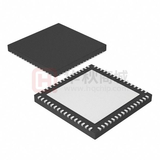
QFN64 9x9mm 0.5mm pitch Exp-pad package
Block Diagram
MIPI CSI-2
Data Tx 4-lane
Clock Tx 2-port
THCV242
MTX0P
V-by-One® HS
Main-Link
Rx 2-lane
MTX0N
MTX1P
RX0P
Sub-Link 2-lane
CSI2 / Formatter
RX1N
Deserializer
RX1P
MTX1N
MTXCLK0P
MTXCLK0N
MTX2P
MTX2N
MTX3P
CDR
RX0N
MTX3N
RCM0P
MTXCLK1P
RCM0N
MTXCLK1N
Settings
RCM1P
RCM1N
Controls
GPIO
2-wire
serial I/F
OSC
Copyright©2019 THine Electronics, Inc.
1/53
THine Electronics, Inc.
Security E
�THCV242_ Rev.2.00_E
Contents page
1.
General Description ......................................................................................................................................... 1
2.
Features ........................................................................................................................................................... 1
3.
Block Diagram ................................................................................................................................................ 1
4.
Pin Configuration ............................................................................................................................................ 4
5.
Pin Description ................................................................................................................................................ 5
6.
Functional Description .................................................................................................................................... 6
6.1.
Functional Overview ............................................................................................................................... 6
6.2.
V-by-One® HS ........................................................................................................................................ 6
V-by-One® HS input setting ........................................................................................................... 6
MPRF (Main-Link PRivate Format) ............................................................................................... 7
V-by-One® HS standard format ...................................................................................................... 8
Link Status (HTPDN/LOCKN) ..................................................................................................... 12
6.3.
Local, Remote and Remote Slave Register Programming .................................................................... 14
2-wire serial I/F slave Device ID ................................................................................................... 14
2-wire serial Read/Write access to local Register.......................................................................... 15
2-wire serial I/F Watch Dog Timer ................................................................................................ 16
Sub-Link setting ............................................................................................................................ 17
Sub-Link 2-wire Read/Write access to remote Register ................................................................ 18
6.3.5.1.
Sub-Link 2-wire Set and Trigger mode ................................................................................. 18
6.3.5.2.
Sub-Link 2-wire Pass Through mode .................................................................................... 21
Sub-Link transaction time accuracy Improvement ........................................................................ 24
6.4.
GPIO setting .......................................................................................................................................... 25
Register GPIO ............................................................................................................................... 26
Through GPIO ............................................................................................................................... 27
GPIO as secondary 2-wire port ..................................................................................................... 28
6.5.
MIPI ...................................................................................................................................................... 29
Deserializer and CSI-2 Formatter .................................................................................................. 29
6.5.1.1.
PLL setting ............................................................................................................................ 29
6.5.1.2.
Video stream switch and copy/distribution............................................................................ 31
Header/Packet/Sync Pre-processing .............................................................................................. 32
MIPI output setting ........................................................................................................................ 33
MIPI CSI-2 Virtual Channel .......................................................................................................... 35
Multiple camera synchronization Frame Vsync supply ................................................................ 36
6.6.
Status monitoring, Interrupt and Error Detection .................................................................................. 38
Internal Error / status signal monitoring pin output....................................................................... 38
Copyright©2019 THine Electronics, Inc.
2/53
THine Electronics, Inc.
Security E
�THCV242_ Rev.2.00_E
Internal Error / status signal monitoring register ........................................................................... 41
Interrupt monitoring ...................................................................................................................... 42
Register Auto Checksum diagnosis ............................................................................................... 43
6.7.
Power On Sequence............................................................................................................................... 44
6.8.
Lock / Re-Lock Sequence ..................................................................................................................... 45
7.
Absolute Maximum Ratings .......................................................................................................................... 46
8.
Recommended Operating Conditions............................................................................................................ 46
9.
Consumption Current .................................................................................................................................... 47
10.
DC Specifications ...................................................................................................................................... 48
10.1.
CMOS DC Specifications.................................................................................................................. 48
10.2.
CML Receiver DC Specifications ..................................................................................................... 48
10.3.
MIPI Transmitter DC Specifications ................................................................................................. 49
10.4.
CML Bi-directional Buffer DC Specifications .................................................................................. 50
11.
AC Specifications ...................................................................................................................................... 51
11.1.
General AC Specifications .................................................................................................................... 51
11.2.
CML Receiver AC Specifications ......................................................................................................... 51
11.3.
MIPI Transmitter AC Specifications ..................................................................................................... 51
11.4.
CML B-directional Buffer AC Specifications ....................................................................................... 51
11.5.
2-wire serial Slave AC Specifications ................................................................................................... 51
12.
Package...................................................................................................................................................... 52
13.
Notices and Requests................................................................................................................................. 53
MIPI is a licensed trademark of MIPI, Inc. in the U.S. and other jurisdictions.
Copyright©2019 THine Electronics, Inc.
3/53
THine Electronics, Inc.
Security E
�THCV242_ Rev.2.00_E
VDDIO1
GPIO7
GPIO6
GPIO5
GPIO4
GPIO3
GPIO2
GPIO1
GPIO0
INT1
INT0
AIN1
AIN0
SDA
SCL
VDDIO1
47
46
45
44
43
42
41
40
39
38
37
36
35
34
33
Pin Configuration
48
ERR0
49
32 EXTSYNC
ERR1
50
31
PDN
30
VDDPLL
THCV242
VDDCORE 51
VDDRX
52
29
VDDTX
RX0N
53
28
MTX3P
RX0P
54
27
MTX3N
VSSRX
55
26
MTX1P
RX1N
56
25
MTX1N
RX1P
57
VDDRX
58
23 MTXCLK0N
RSVDL0
59
22
MTX0P
RSVDL0
60
21
MTX0N
VSSRX
61
20
MTX2P
RSVDL0
62
19
MTX2N
RSVDL0
63
VDDRX
64
(TOP VIEW)
65 EXPGND
24 MTXCLK0P
●
18 MTXCLK1P
4/53
16
VDDTX
VDDCORE 15
8
RSVDL2
RSVDL2 14
7
RSVDL2
RSVDT1L2 13
6
RCM1P
RSVDT2H2 12
5
RCM1N
VDDIO2 11
4
RCM0P
RSVDL2 10
3
RCM0N
Copyright©2019 THine Electronics, Inc.
9
2
VDDIO2
VDDCORE 1
17 MTXCLK1N
RSVDL2
4.
THine Electronics, Inc.
Security E
�THCV242_ Rev.2.00_E
5.
Pin Description
Pin Name
RX0P/N
RX1P/N
RCM0P/N
RCM1P/N
MTX0P/N
MTX1P/N
MTX2P/N
MTX3P/N
MTXCLK0P/N
MTXCLK1P/N
RSVDT1L2
RSVDT2H2
Pin #
54, 53
57, 56
4, 3
6, 5
22, 21
26, 25
20, 19
28, 27
24, 23
18, 17
13
12
type*
CI
CI
CB
CB
MO
MO
MO
MO
MO
MO
I2
I2
PDN
31
I1
AIN1
37
I1
AIN0
36
I1
SCL
SDA
GPIO0
GPIO1
GPIO2
GPIO3
GPIO4
GPIO5
GPIO6
GPIO7
34
35
40
41
42
43
44
45
46
47
B
B
B
B
B
B
B
B
B
B
INT0
38
O
INT1
39
O
Description
V-by-One® HS Input lane0
V-by-One® HS Input lane1
CML Bi-directiona Input/Output (Sub-Link).
CML Bi-directiona Input/Output (Sub-Link).
MIPI differential data outputs lane0
MIPI differential data outputs lane1
MIPI differential data outputs lane2
MIPI differential data outputs lane3
MIPI differential clock outputs lane0
MIPI differential clock outputs lane1
Reserved Pin, Must be tied to ground for normal operation.
Reserved pin. Must be tied to VDDIO2 for normal operation.
Pow er Dow n (User Pow er On Reset control must be reuiquired.)
0: Pow er Dow n Mode
1: Normal Operation
Device Address Setting for 2-w ire Serial Interface
[AIN1:AIN0]=00: ID=7'h0B
[AIN1:AIN0]=01: ID=7'h34
[AIN1:AIN0]=10: ID=7'h77
[AIN1:AIN0]=11: ID=7'h65
2-w ire Serial Interface clock line
2-w ire Serial Interface data line
General Purpose Input/Output
General Purpose Input/Output
General Purpose Input/Output
General Purpose Input/Output
General Purpose Input/Output
General Purpose Input/Output
General Purpose Input/Output
General Purpose Input/Output
Interrupt signal output.
It must be connected w ith a pull-up resistor.
0 : Interrupt occurred
1 : Steady state
ERR0
49
O
Internal Error / status signal monitoring output
ERR1
50
O
Internal Error / status signal monitoring output
EXTSYNC
32
B
External Sync input/output for multiple camera syncronization
RSVDL0
59, 60, 62, 63
I0
Reserved Pins, Must be tied to ground for normal operation.
RSVDL2
7, 8, 9, 10, 14
I2
Reserved Pins, Must be tied to ground for normal operation.
VDDIO1
33, 48
P
Pow er Supply for CMOS I/O
VDDIO2
2,11
P
Pow er Supply for Sub-Link I/O
VDDCORE
1,15,51
P
Pow er Supply for Digital Circuit
VDDRX
52,58,64
P
Pow er Supply for Analog Circuit
VSSRX
55,61
G
GND for Analog Circuit
VDDTX
16,29
P
Pow er Supply for Analog Circuit
VDDPLL
30
P
Pow er Supply for Analog Circuit
EXPGND
65
G
Exposed GND Pad
*type symbol ; MO=MIPI Output, CI=CML Input, CB=CML Bi-directional input/output
I0=1.2V CMOS Input, I1=1.8~3.3V VDDIO1 domain CMOS Input, I2=1.8~3.3V VDDIO2 domain CMOS Input
O=1.8~3.3V VDDIO1 domain CMOS Output, B=1.8~3.3V VDDIO1 domain CMOS Bi-directional input/output
P=Pow er, G=Ground
Copyright©2019 THine Electronics, Inc.
5/53
THine Electronics, Inc.
Security E
�THCV242_ Rev.2.00_E
6.
6.1.
Functional Description
Functional Overview
THCV242 can receive CML video signal transmitted over 15m length and encode it to MIPI CSI-2 format. With
High Speed CML SerDes, high reliability and robustness encoding scheme and CDR (Clock and Data Recovery)
architecture, the THCV242 enables to receive RAW/YUV/RGB/JPEG/Generic8bit data through Main-Link by
single 100ohm differential pair or 50ohm Coax cable with minimal external components. In addition, THCV242
has Sub-Link which enables bi-directional transmission of 2-wire serial interface signals, GPIO signals and also
HTPDN/LOCKN signals for Main-Link through the other 1-pair of CML-Line. The THCV242 system is able to
watch remote devices and to control them via 2-wire serial interface or GPIOs. They also can report interrupt
events caused by change of remote device statuses and internal statuses such as CRC error.
6.2.
V-by-One® HS
V-by-One® HS input setting
Setting of V-by-One® HS input format can be configurable by 2-wire access to internal register.
Table 1. V-by-One® HS input format setting
Adr
0x10 10
bit
[7:6]
0x10 10
[5:4]
0x10 12
[4]
0x10 12
Register Name
R_MLNK_NHSEL0
width R/W
2
R/W
Description
init
2'h2 V-by-One® Main-Link Mode Select (for LINK0)
R_MLNK_COL0
2
R/W
2'h1
R_RGB565_ON_L0
1
R/W
1'b0
[3:0]
R_VX1_LANE_FMT0
4
R/W
4'h0
0x10 14
[7:6]
R_VRZ_NHSEL1
2
R/W
2'h2
0x10 14
[5:4]
R_VRZ_COL1
2
R/W
2'h1
Copyright©2019 THine Electronics, Inc.
00 : Reserved
01 : Reserved
10 : V-by-One® HS standard mode
11 : Reserved
V-by-One® Main-Link Byte Mode Select (for LINK0)
00 : Reserved
01 : 8bit (3Byte mode)
10 : 10bit (4Byte mode)
11 : Reserved
Main-Link Input Data Format Setting2
(This register could use only w hen R_VX1_LANE_FMT0=0x1)
0: RGB888
1: RGB565
Main-Link Input Data Format Setting
0: MPRF
1: RGBxxx
2,3,4,5,6: YUV422 (NormalYU1,NormalYU2,NormalYU3,DemuxYU1,DemuxYU2)
7,8,9: RAW8 (NormalR081,NormalR082,DemuxR081)
10,11,12: RAW10 (NormalR101,DemuxR101,DemuxR102)
13,14,15: RAW12 (NormalR121,DemuxR121,DemuxR122)
V-by-One® Main-Link Mode Select (for LINK1)
00 : Reserved
01 : Reserved
10 : V-by-One® HS standard mode
11 : Reserved
V-by-One® Main-Link Byte Mode Select (for LINK1)
00 : Reserved
01 : 8bit (3Byte mode)
10 : 10bit (4Byte mode)
11 : Reserved
6/53
THine Electronics, Inc.
Security E
�THCV242_ Rev.2.00_E
MPRF (Main-Link PRivate Format)
MPRF format encoding preserves original data packet input to V-by-One® HS transmitter and output the data
packet from THCV242. The counterpart transmitter must have installed MPRF format decoder like THCV241
because MPRF is not standard format.
Input V-by-One® HS Byte Mode is 4Byte Mode.
Video formats: RAW8/10/12/14/16/20, YUV422/420, RGB888/666/565, JPEG, and User-defined generic 8-bit
are all supported with MPRF.
CMOS Sensor
Original
Data packet
(format,
payload, etc.)
THCV241
Figure 1.
Copyright©2019 THine Electronics, Inc.
Main-Link
MPRF
format
THCV242
Preserved
Data packet
(format,
payload, etc.)
Processor
In ECU or
controller
MPRF (Main-Link PRivate Format)
7/53
THine Electronics, Inc.
Security E
�THCV242_ Rev.2.00_E
V-by-One® HS standard format
THCV242 input format capabilities as receiver are shown as follows. D[31:0] indicates V-by-One® HS standard
version1.5 UnPacker packet definition. Data can be transmitted normally only when both transmitter and receiver
are set to the same available format. Some of the THCV242 format may not be supported by particular counterpart
transmitter because THCV242 prepares multiple formats that suit to multiple transmitter devices alternatives.
Table 2. V-by-One® HS input data mapping format 1/4
Format Name
Vx1HS std. Packer Packet ref.
V-by-One®HS_D[31]
V-by-One®HS_D[30]
V-by-One®HS_D[29]
V-by-One®HS_D[28]
V-by-One®HS_D[27]
V-by-One®HS_D[26]
V-by-One®HS_D[25]
V-by-One®HS_D[24]
V-by-One®HS_D[23]
V-by-One®HS_D[22]
V-by-One®HS_D[21]
V-by-One®HS_D[20]
V-by-One®HS_D[19]
V-by-One®HS_D[18]
V-by-One®HS_D[17]
V-by-One®HS_D[16]
V-by-One®HS_D[15]
V-by-One®HS_D[14]
V-by-One®HS_D[13]
V-by-One®HS_D[12]
V-by-One®HS_D[11]
V-by-One®HS_D[10]
V-by-One®HS_D[9]
V-by-One®HS_D[8]
V-by-One®HS_D[7]
V-by-One®HS_D[6]
V-by-One®HS_D[5]
V-by-One®HS_D[4]
V-by-One®HS_D[3]
V-by-One®HS_D[2]
V-by-One®HS_D[1]
V-by-One®HS_D[0]
RGB888
0
0
0
0
0
0
0
0
B[7]
B[6]
B[5]
B[4]
B[3]
B[2]
B[1]
B[0]
G[7]
G[6]
G[5]
G[4]
G[3]
G[2]
G[1]
G[0]
R[7]
R[6]
R[5]
R[4]
R[3]
R[2]
R[1]
R[0]
Copyright©2019 THine Electronics, Inc.
Normal Mode1
0
0
0
0
0
0
0
0
0
0
0
0
0
0
0
0
Y[7]
Y[6]
Y[5]
Y[4]
Y[3]
Y[2]
Y[1]
Y[0]
Cb[7]/Cr[7]
Cb[6]/Cr[6]
Cb[5]/Cr[5]
Cb[4]/Cr[4]
Cb[3]/Cr[3]
Cb[2]/Cr[2]
Cb[1]/Cr[1]
Cb[0]/Cr[0]
Normal Mode2
0
0
0
0
0
0
0
0
Cb[7]/Cr[7]
Cb[6]/Cr[6]
Cb[5]/Cr[5]
Cb[4]/Cr[4]
Cb[3]/Cr[3]
Cb[2]/Cr[2]
Cb[1]/Cr[1]
Cb[0]/Cr[0]
0
0
0
0
0
0
0
0
Y[7]
Y[6]
Y[5]
Y[4]
Y[3]
Y[2]
Y[1]
Y[0]
8/53
YUV422
Normal Mode3
0
0
0
0
0
0
0
0
Y[7]
Y[6]
Y[5]
Y[4]
Y[3]
Y[2]
Y[1]
Y[0]
0
0
0
0
0
0
0
0
Cb[7]/Cr[7]
Cb[6]/Cr[6]
Cb[5]/Cr[5]
Cb[4]/Cr[4]
Cb[3]/Cr[3]
Cb[2]/Cr[2]
Cb[1]/Cr[1]
Cb[0]/Cr[0]
Demux Mode1
Y[7](1st pixel)
Y[6](1st pixel)
Y[5](1st pixel)
Y[4](1st pixel)
Y[3](1st pixel)
Y[2](1st pixel)
Y[1](1st pixel)
Y[0](1st pixel)
Cb[7]
Cb[6]
Cb[5]
Cb[4]
Cb[3]
Cb[2]
Cb[1]
Cb[0]
Y[7](2nd pixel)
Y[6](2nd pixel)
Y[5](2nd pixel)
Y[4](2nd pixel)
Y[3](2nd pixel)
Y[2](2nd pixel)
Y[1](2nd pixel)
Y[0](2nd pixel)
Cr[7]
Cr[6]
Cr[5]
Cr[4]
Cr[3]
Cr[2]
Cr[1]
Cr[0]
Demux Mode2
Cb[7]
Cb[6]
Cb[5]
Cb[4]
Cb[3]
Cb[2]
Cb[1]
Cb[0]
Y[7](1st pixel)
Y[6](1st pixel)
Y[5](1st pixel)
Y[4](1st pixel)
Y[3](1st pixel)
Y[2](1st pixel)
Y[1](1st pixel)
Y[0](1st pixel)
Cr[7]
Cr[6]
Cr[5]
Cr[4]
Cr[3]
Cr[2]
Cr[1]
Cr[0]
Y[7](2nd pixel)
Y[6](2nd pixel)
Y[5](2nd pixel)
Y[4](2nd pixel)
Y[3](2nd pixel)
Y[2](2nd pixel)
Y[1](2nd pixel)
Y[0](2nd pixel)
THine Electronics, Inc.
Security E
�THCV242_ Rev.2.00_E
Table 3. V-by-One® HS input data mapping format 2/4
Format Name
Vx1HS std. Packer Packet ref.
V-by-One®HS_D[31]
V-by-One®HS_D[30]
V-by-One®HS_D[29]
V-by-One®HS_D[28]
V-by-One®HS_D[27]
V-by-One®HS_D[26]
V-by-One®HS_D[25]
V-by-One®HS_D[24]
V-by-One®HS_D[23]
V-by-One®HS_D[22]
V-by-One®HS_D[21]
V-by-One®HS_D[20]
V-by-One®HS_D[19]
V-by-One®HS_D[18]
V-by-One®HS_D[17]
V-by-One®HS_D[16]
V-by-One®HS_D[15]
V-by-One®HS_D[14]
V-by-One®HS_D[13]
V-by-One®HS_D[12]
V-by-One®HS_D[11]
V-by-One®HS_D[10]
V-by-One®HS_D[9]
V-by-One®HS_D[8]
V-by-One®HS_D[7]
V-by-One®HS_D[6]
V-by-One®HS_D[5]
V-by-One®HS_D[4]
V-by-One®HS_D[3]
V-by-One®HS_D[2]
V-by-One®HS_D[1]
V-by-One®HS_D[0]
Copyright©2019 THine Electronics, Inc.
RAW8
Normal Mode2
0
0
0
0
0
0
0
0
RAW[7] (1st pixel)
RAW[6] (1st pixel)
RAW[5] (1st pixel)
RAW[4] (1st pixel)
RAW[3] (1st pixel)
RAW[2] (1st pixel)
RAW[1] (1st pixel)
RAW[0] (1st pixel)
0
0
0
0
0
0
0
0
RAW[7] (2nd pixel)
RAW[6] (2nd pixel)
RAW[5] (2nd pixel)
RAW[4] (2nd pixel)
RAW[3] (2nd pixel)
RAW[2] (2nd pixel)
RAW[1] (2nd pixel)
RAW[0] (2nd pixel)
Normal Mode1
0
0
0
0
0
0
0
0
0
0
0
0
0
0
0
0
RAW[7] (2nd pixel)
RAW[6] (2nd pixel)
RAW[5] (2nd pixel)
RAW[4] (2nd pixel)
RAW[3] (2nd pixel)
RAW[2] (2nd pixel)
RAW[1] (2nd pixel)
RAW[0] (2nd pixel)
RAW[7] (1st pixel)
RAW[6] (1st pixel)
RAW[5] (1st pixel)
RAW[4] (1st pixel)
RAW[3] (1st pixel)
RAW[2] (1st pixel)
RAW[1] (1st pixel)
RAW[0] (1st pixel)
9/53
Demux Mode1
RAW[7] (2nd pixel)
RAW[6] (2nd pixel)
RAW[5] (2nd pixel)
RAW[4] (2nd pixel)
RAW[3] (2nd pixel)
RAW[2] (2nd pixel)
RAW[1] (2nd pixel)
RAW[0] (2nd pixel)
RAW[7] (1st pixel)
RAW[6] (1st pixel)
RAW[5] (1st pixel)
RAW[4] (1st pixel)
RAW[3] (1st pixel)
RAW[2] (1st pixel)
RAW[1] (1st pixel)
RAW[0] (1st pixel)
RAW[7] (4th pixel)
RAW[6] (4th pixel)
RAW[5] (4th pixel)
RAW[4] (4th pixel)
RAW[3] (4th pixel)
RAW[2] (4th pixel)
RAW[1] (4th pixel)
RAW[0] (4th pixel)
RAW[7] (3rd pixel)
RAW[6] (3rd pixel)
RAW[5] (3rd pixel)
RAW[4] (3rd pixel)
RAW[3] (3rd pixel)
RAW[2] (3rd pixel)
RAW[1] (3rd pixel)
RAW[0] (3rd pixel)
THine Electronics, Inc.
Security E
�THCV242_ Rev.2.00_E
Table 4. V-by-One® HS input data mapping format 3/4
Format Name
Vx1HS std. Packer Packet ref.
V-by-One®HS_D[31]
V-by-One®HS_D[30]
V-by-One®HS_D[29]
V-by-One®HS_D[28]
V-by-One®HS_D[27]
V-by-One®HS_D[26]
V-by-One®HS_D[25]
V-by-One®HS_D[24]
V-by-One®HS_D[23]
V-by-One®HS_D[22]
V-by-One®HS_D[21]
V-by-One®HS_D[20]
V-by-One®HS_D[19]
V-by-One®HS_D[18]
V-by-One®HS_D[17]
V-by-One®HS_D[16]
V-by-One®HS_D[15]
V-by-One®HS_D[14]
V-by-One®HS_D[13]
V-by-One®HS_D[12]
V-by-One®HS_D[11]
V-by-One®HS_D[10]
V-by-One®HS_D[9]
V-by-One®HS_D[8]
V-by-One®HS_D[7]
V-by-One®HS_D[6]
V-by-One®HS_D[5]
V-by-One®HS_D[4]
V-by-One®HS_D[3]
V-by-One®HS_D[2]
V-by-One®HS_D[1]
V-by-One®HS_D[0]
Copyright©2019 THine Electronics, Inc.
RAW10
Demux Mode1
0
0
0
0
0
0
RAW[1](1st pixel)
RAW[0](1st pixel)
RAW[9](1st pixel)
RAW[8](1st pixel)
RAW[7](1st pixel)
RAW[6](1st pixel)
RAW[5](1st pixel)
RAW[4](1st pixel)
RAW[3](1st pixel)
RAW[2](1st pixel)
0
0
0
0
0
0
RAW[1](2nd pixel)
RAW[0](2nd pixel)
RAW[9](2nd pixel)
RAW[8](2nd pixel)
RAW[7](2nd pixel)
RAW[6](2nd pixel)
RAW[5](2nd pixel)
RAW[4](2nd pixel)
RAW[3](2nd pixel)
RAW[2](2nd pixel)
Normal
0
0
0
0
0
0
0
0
0
0
0
0
0
0
0
0
0
0
0
0
0
0
RAW[1]
RAW[0]
RAW[9]
RAW[8]
RAW[7]
RAW[6]
RAW[5]
RAW[4]
RAW[3]
RAW[2]
10/53
Demux Mode2
0
0
0
0
0
0
0
0
0
0
RAW[1](1st pixel)
RAW[0](1st pixel)
RAW[9](1st pixel)
RAW[8](1st pixel)
RAW[7](1st pixel)
RAW[6](1st pixel)
RAW[5](1st pixel)
RAW[4](1st pixel)
RAW[3](1st pixel)
RAW[2](1st pixel)
0
0
RAW[1](2nd pixel)
RAW[0](2nd pixel)
RAW[9](2nd pixel)
RAW[8](2nd pixel)
RAW[7](2nd pixel)
RAW[6](2nd pixel)
RAW[5](2nd pixel)
RAW[4](2nd pixel)
RAW[3](2nd pixel)
RAW[2](2nd pixel)
THine Electronics, Inc.
Security E
�THCV242_ Rev.2.00_E
Table 5. V-by-One® HS input data mapping format 4/4
Format Name
Vx1HS std. Packer Packet ref.
V-by-One®HS_D[31]
V-by-One®HS_D[30]
V-by-One®HS_D[29]
V-by-One®HS_D[28]
V-by-One®HS_D[27]
V-by-One®HS_D[26]
V-by-One®HS_D[25]
V-by-One®HS_D[24]
V-by-One®HS_D[23]
V-by-One®HS_D[22]
V-by-One®HS_D[21]
V-by-One®HS_D[20]
V-by-One®HS_D[19]
V-by-One®HS_D[18]
V-by-One®HS_D[17]
V-by-One®HS_D[16]
V-by-One®HS_D[15]
V-by-One®HS_D[14]
V-by-One®HS_D[13]
V-by-One®HS_D[12]
V-by-One®HS_D[11]
V-by-One®HS_D[10]
V-by-One®HS_D[9]
V-by-One®HS_D[8]
V-by-One®HS_D[7]
V-by-One®HS_D[6]
V-by-One®HS_D[5]
V-by-One®HS_D[4]
V-by-One®HS_D[3]
V-by-One®HS_D[2]
V-by-One®HS_D[1]
V-by-One®HS_D[0]
Copyright©2019 THine Electronics, Inc.
RAW12
Demux Mode1
0
0
0
0
RAW[3](1st pixel)
RAW[2](1st pixel)
RAW[1](1st pixel)
RAW[0](1st pixel)
RAW[11](1st pixel)
RAW[10](1st pixel)
RAW[9](1st pixel)
RAW[8](1st pixel)
RAW[7](1st pixel)
RAW[6](1st pixel)
RAW[5](1st pixel)
RAW[4](1st pixel)
0
0
0
0
RAW[3](2nd pixel)
RAW[2](2nd pixel)
RAW[1](2nd pixel)
RAW[0](2nd pixel)
RAW[11](2nd pixel)
RAW[10](2nd pixel)
RAW[9](2nd pixel)
RAW[8](2nd pixel)
RAW[7](2nd pixel)
RAW[6](2nd pixel)
RAW[5](2nd pixel)
RAW[4](2nd pixel)
Normal
0
0
0
0
0
0
0
0
0
0
0
0
0
0
0
0
0
0
0
0
RAW[3]
RAW[2]
RAW[1]
RAW[0]
RAW[11]
RAW[10]
RAW[9]
RAW[8]
RAW[7]
RAW[6]
RAW[5]
RAW[4]
11/53
Demux Mode2
0
0
0
0
0
0
0
0
RAW[3](1st pixel)
RAW[2](1st pixel)
RAW[1](1st pixel)
RAW[0](1st pixel)
RAW[11](1st pixel)
RAW[10](1st pixel)
RAW[9](1st pixel)
RAW[8](1st pixel)
RAW[7](1st pixel)
RAW[6](1st pixel)
RAW[5](1st pixel)
RAW[4](1st pixel)
RAW[3](2nd pixel)
RAW[2](2nd pixel)
RAW[1](2nd pixel)
RAW[0](2nd pixel)
RAW[11](2nd pixel)
RAW[10](2nd pixel)
RAW[9](2nd pixel)
RAW[8](2nd pixel)
RAW[7](2nd pixel)
RAW[6](2nd pixel)
RAW[5](2nd pixel)
RAW[4](2nd pixel)
THine Electronics, Inc.
Security E
�THCV242_ Rev.2.00_E
Link Status (HTPDN/LOCKN)
Hot-Plug Function
HTPDN indicates Main-Link connect condition between Transmitter and Receiver. HTPDN of Transmitter side
is high when Receiver is not active or not connected. Then Transmitter can enter into power down mode. HTPDN
is set to Low by the Receiver when Receiver is active and connects to the Transmitter, and then Transmitter must
start up and transmit CDR training pattern for link training. HTPDN is open drain output at the receiver side.
Transmitter side needs Pull-up resistor.
There is an application option to omit HTPDN connection between Transmitter and Receiver. In this case,
HTPDN at Transmitter side should always be at Low.
Lock Detect Function
LOCKN indicates whether CDR PLL of Main-Link is in lock status or not. LOCKN at Transmitter input is set
to High by pull-up resistor when Receiver is not active or in CDR PLL training. LOCKN is set to Low by Receiver
when CDR lock is completed. After that the CDR training mode finishes and then Transmitter shifts to the normal
mode. LOCKN of Receiver is open drain. Transmitter side needs pull-up resistor.
When an application omits HTPDN, LOCKN signal should only be considered with HTPDN pulled low by
Receiver.
Vcc
(Tx side)
V-by-One®
HS Tx
THCV242
30kΩ
THCV242
30kΩ
V-by-One®
HS Tx
30kΩ
Vcc
(Tx side)
HTPDN
ERRy
(HTPDN)
HTPDN
HTPDN
LOCKN
ERRx
(LOCKN)
LOCKN
ERRx
(LOCKN)
With HTPDN connect
Figure 2.
Without HTPDN connect
Physical wire connection for wired Hot-plug and Lock detect scheme
It will need same GND potential reference between transmitter and receiver device to connect HTPDN and
LOCKN pins directly like above. HTPDN and LOCKN can also be transmitted via Sub-Link without physical
wire connection. Assignment can be configurable by 2-wire access to internal register.
Copyright©2019 THine Electronics, Inc.
12/53
THine Electronics, Inc.
Security E
�THCV242_ Rev.2.00_E
Table 6. HTPDN/LOCKN register
Addr(h)
0x0019
bit
Register Name
width
[7:4] ReservedL
4
[3:2] R_LOCKN_LN1_SEL
2
[1:0] R_LOCKN_LN0_SEL
2
Copyright©2019 THine Electronics, Inc.
R/W
Description
Default
RW Must be set 0
Sub-Link Lane1 LOCKN/HTPDN scheme of releted Main-Link select
0:LOCKN1
1:LOCKN0 | LOCKN1
RW 2:Reserved
3:1'b0 (Forced LOCKN/HTPDN=Low)
*LOCKN1=LOCKN signal of V-by-One(R) HS Lane1=RX1P/RX1N
*HTPDN of the same lane as above set LOCKN lane is used
Sub-Link Lane0 LOCKN/HTPDN scheme of releted Main-Link select
0:LOCKN0
1:LOCKN0 | LOCKN1
RW 2:Reserved
3:1'b0 (Forced LOCKN/HTPDN=Low)
*LOCKN0=LOCKN signal of V-by-One(R) HS Lane0=RX0P/RX0N
*HTPDN of the same lane as above set LOCKN lane is used
13/53
4'd0
2'd0
2'd0
THine Electronics, Inc.
Security E
�THCV242_ Rev.2.00_E
6.3.
Local, Remote and Remote Slave Register Programming
2-wire serial I/F slave Device ID
To use basic functions, initialization, GPIO (General Purpose Input/Output), fault/error detection, and interrupt
function, 2-wire serial I/F enables to access registers. AIN pin determines 2-wire slave Device ID setting.
Table 7. 2-wire serial I/F Device ID select by AIN pin
AIN1
37
I1
AIN0
36
I1
Device Address Setting for 2-w ire Serial Interface
[AIN1:AIN0]=00: ID=7'h0B
[AIN1:AIN0]=01: ID=7'h34
[AIN1:AIN0]=10: ID=7'h77
[AIN1:AIN0]=11: ID=7'h65
As an additional method, 2-wire slave Device ID setting can be changed from default value by register setting.
Table 8. 2-wire serial I/F Device ID select by register setting
Addr(h)
0x0030
bit
Register Name
[7:0] R_2WIRE_SADR
width
8
Copyright©2019 THine Electronics, Inc.
R/W
Description
Default
2WIRE slave device address setting
[7]2WIRE slave device address control
RW 0: 2WIRE slv device addr. is set by AIN pin
1: 2WIRE slv device addr. is set by following register [6:0]
[6:0]2WIRE slave device address value for register control
14/53
8'd0
THine Electronics, Inc.
Security E
�THCV242_ Rev.2.00_E
2-wire serial Read/Write access to local Register
HOST MPU can directly access THCV242 local register by 2-wire serial I/F.
THCV242
Sub-Link Block
Sub-Link
Master
2-wire
Slave
SCL
Host
MPU
SDA
Registe r
AIN = Use r S elect
Figure 3.
S
Device ID
Host to THCV242 local register access configuration
W A Register address MSB
Device ID
Register address LSB
A
Write data #1
A
...
A P
W Write command indicator
S
Start condition
P
Stop condition
Access from 2-wire serial interface Master
A
ACK
Access from 2-wire serial interface Slave
A
NACK
Figure 4.
S
A
2-wire serial I/F write to THCV242 local register protocol
W A Register address MSB
A
Register address LSB
S
Start condition
R Read command indicator
P
Stop condition
W Write command indicator
A
ACK
Access from 2-wire serial interface Master
A
NACK
Access from 2-wire serial interface Slave
A Sr
Device ID
R A
Read data #1
A
...
A P
Sr Repeated start condition
Figure 5.
Copyright©2019 THine Electronics, Inc.
2-wire serial I/F read to THCV242 local register protocol
15/53
THine Electronics, Inc.
Security E
�THCV242_ Rev.2.00_E
2-wire serial I/F Watch Dog Timer
2-wire Watch Dog Timer (WDT) is installed to monitor status.
Table 9. 2-wire WDT setting
Addr(h)
0x003B
bit
Register Name
[7:5] reserved
[4]
R_2WIRE_WD_EN
[3:1] reserved
[0]
0x003C
R_2WIRE_WD_OFFSET
[7:0] R_2WIRE_WD_TIM
width
R/W
3
-
1
3
1
8
Copyright©2019 THine Electronics, Inc.
Description
Default
2WIRE WDT Enable
RW 0:Disable
1:Enable
- 2WIRE_WDT_OffsetTime
RW 1:11'd2047
0:11'd1023
RW 2WIRE WDT_time=64×{R_2WIRE_WD_TIM+1}×{2WIRE_WDT_OffsetTime}×tOSC
16/53
1'b1
1'd1
8'd255
THine Electronics, Inc.
Security E
�THCV242_ Rev.2.00_E
Sub-Link setting
THCV242 has Sub-Link which enables bi-directional transmission of 2-wire serial interface signals, GPIO
signals and also HTPDN/LOCKN signals for Main-Link. THCV242 is Sub-Link Master and connectable to SubLink Slave device such as THCV241.
Sub-Link Polling interval is controllable from about 20us to 800us, that may have relationships on fault/error
detection, interrupt, or other UART / GPIO transfer time designed on application. SSR (Sub-Link Status Read)
interval determines recovery quickness from 2-wire serial remote communication completion. SSR interval
effects only on Sub-Link Master “2-wire Set&Trigger mode1” (R_SLINK_MODE setting).
Table 10. Sub-Link Master protocol basic setting
Addr(h)
0x0004
0x0010
0x0011
0x001A
width
R/W
[7:3] reserved
bit
5
-
[2:0] R_SLINK_MODE
3
RW
[7:4] R_SLINK_EN
4
RW
[3:0] R_SLINK_POL_EN
4
RW
[7:4] R_SLINK_SSR_EN
4
RW
[3:0] R_SLINK_WD_EN
4
RW
[7:5] reserved
3
-
1
RW
[4]
Register Name
R_SLINK_POL_OFSET_EN
[3:2] reserved
2
[1:0] R_SLINK_POL_TIM_UP
2
0x001B
[7:0] R_SLINK_POL_TIM_DN
8
0x001C
[7:2] reserved
[1:0] R_SLINK_SSR_TIM_UP
6
2
0x001D
[7:0] R_SLINK_SSR_TIM_DN
8
-
Description
Default
Sub-Link basic protocol setting as Sub-Link Master
1: 2-wire Set&Trigger (Normal) mode1
3: 2-wire Pass Through mode1
0,2,4,5,6,7: Reserved
Sub-Link Enable
[7] Reserved
[6] Reserved
[5] 0:Lane1 Disable, 1:Lane1 Enable
[4] 0:Lane0 Disable, 1:Lane0 Enable
Sub-Link Polling Enable
[3] Reserved
[2] Reserved
[1] 0:Lane1 Disable, 1:Lane1 Enable
[0] 0:Lane0 Disable, 1:Lane0 Enable
Sub-Link SSR Enable
[7] Reserved
[6] Reserved
[5] 0:Lane1 Disable, 1:Lane1 Enable
[4] 0:Lane0 Disable, 1:Lane0 Enable
Sub-Link WDT Enable
[3] Reserved
[2] Reserved
[1] 0:Lane1 Disable, 1:Lane1 Enable
[0] 0:Lane0 Disable, 1:Lane0 Enable
Sub-Link Polling Offset Enable
0:Disable
1:Enable, Polling time phase of each lanes are shifted as below
lane1 offset from lane0: Sub-Link Poling interval x 1/4
3'd1
4'd0
4'hF
4'hF
4'hF
1'b0
-
-
RW Sub-Link Polling interval setting (min. 0x018, about 20us)
Sub-Link Polling interval time=64×(256×R_SLINK_POL_TIM_UP
RW +R_SLINK_POL_TIM_DN+1)×tOSC
*No Polling when R_SLINK_POL_TIM_UP=0 and R_SLINK_POL_TIM_DN=0
- RW Sub-Link SSR interval setting
Sub-Link SSR interval time=64×(256×R_SLINK_SSR_TIM_UP
RW +R_SLINK_SSR_TIM_DN+1)×tOSC
*No SSR when R_SLINK_SSR_TIM_UP=0 and R_SLINK_SSR_TIM_DN=0
2'd0
8'd124
2'd0
8'd249
To use GPIO (General Purpose Input/Output) pin, fault/error detection and interrupt function, “2-wire
Set&Trigger mode1”, “2-wire Pass Through mode1” enables remote register access. THCV242, Sub-Link Master
device has 2-wire serial slave block and can connect to HOST MPU. On the other hand, the counterpart Sub-Link
Slave device has 2-wire serial master block and can connect to remote side 2-wire serial slave devices.
HOST MPU can access register of Sub-Link Master device, Sub-Link Slave device and remote side 2-wire serial
slave devices.
Copyright©2019 THine Electronics, Inc.
17/53
THine Electronics, Inc.
Security E
�THCV242_ Rev.2.00_E
Sub-Link 2-wire Read/Write access to remote Register
6.3.5.1.
Sub-Link 2-wire Set and Trigger mode
HOST MPU can access to Sub-Link Slave’s register via THCV242 as Sub-Link Master only by THCV242
internal local register control and monitoring on 2-wire Set&Trigger mode1.
Sub-Link Slave Device
THCV242 as S ub-Link Master
Sub-Link Block
Sub-Link Block
Sub-Link
line
2-wire
Master
Sub-Link
Slave
Sub-Link
Master
SCL
2-wire
Slave
Host
MPU
SDA
INT
Registe r
Registe r
(MSSEL=1)
Interrupt signal
Trigge red acces s by Sub-Link Master
Access fro m/to HOS T
Figure 6.
AIN = Use r S elect
Host MPU to Sub-Link Slave Register via THCV242 access configuration
HOST MPU can access to remote side 2-wire serial slave register via THCV242 as Sub-Link Master only by
THCV242 internal local register control and monitoring on 2-wire Set&Trigger mode1.
Sub-Link Slave Device
THCV242 as S ub-Link Master
Sub-Link Block
2-wire
Slave
Device#a
SCL
SDA
2-wire
Master
Sub-Link Block
Sub-Link
Slave
Sub-Link
line
Sub-Link
Master
SCL
2-wire
Slave
SDA
Host
MPU
INT
・
・
Registe r
2-wire
Slave
Device#b
(MSSEL=1)
Figure 7.
Registe r
Trigge red acces s by Sub-Link Master
Access fro m/to HOS T
Interrupt signal
AIN = Use r S elect
Host MPU to remote 2-wire slave devices via THCV242 access configuration
Copyright©2019 THine Electronics, Inc.
18/53
THine Electronics, Inc.
Security E
�THCV242_ Rev.2.00_E
In principle, when Sub-Link bridges 2-wire serial interface communication from Sub-Link Master to Sub-Link
Slave or remote side 2-wire serial slave devices, time lag occurs between HOST MPU side 2-wire serial access
and Sub-Link Slave internal bus access or remote side 2-wire serial access.
R_2WIRE_CLKSEN (Sub-Link Master side register, 0x0042 bit0) selects whether 2-wire serial slave of SubLink Master perform clock stretching.
When R_2WIRE_CLKSEN = 1, Sub-Link Master device waits HOST MPU until Sub-Link Slave register access
or remote side 2-wire serial slave register access complete by clock stretching.
When R_2WIRE_CLKSEN = 0, Sub-Link Master device informs HOST MPU that Sub-Link Slave register
access or remote side 2-wire serial register access has completed by interruption (detectable on INT pin) without
clock stretching.
R_2WIRE_CLKSEN=1 (Clock Stretching Enable)
Access start to Sub-Link Slave’s register or
Remote side 2-wire serial Slave’s register
Stop
Condition
SD0
...
(SDA)
2-wire Write
A
SD1
...
(SCL)
Clock Stretching
Sub-Link Slave register Access or
Remote side 2-wire serial register
Access completion
R_2WIRE_CLKSEN=0 (No Clock Stretching)
Access start to Sub-Link Slave’s register or
Remote side 2-wire serial Slave’s register
Stop
Condition
SD0
...
(SDA)
2-wire Write
A
SD1
...
(SCL)
Interruption
INT
Sub-Link communication time + Sub-Link Slave side internal bus access process time
or
Sub-Link communication time + Remote side 2-wire serial Access Time
Figure 8.
Copyright©2019 THine Electronics, Inc.
Sub-Link Master 2-wire slave clock stretching operation
19/53
THine Electronics, Inc.
Security E
�THCV242_ Rev.2.00_E
Table 11. 2-wire serial I/F Set& Trigger mode remote access control and monitoring local registers
Addr(h)
bit
0x00D0
0x00D1
0x00D2
0x00D3
0x00D4
0x00D5
0x00D6
0x00D7
0x00D8
0x00D9
0x00DA
0x00DB
0x00DC
0x00DD
0x00DE
0x00DF
[7:0]
[7:0]
[7:0]
[7:0]
[7:0]
[7:0]
[7:0]
[7:0]
[7:0]
[7:0]
[7:0]
[7:0]
[7:0]
[7:0]
[7:0]
[7:0]
0x00E0
[7:1] R_2WIRE_DEVADR
0x00E1
0x00E2
0x00E4
0x00E5
width
R/W
8
8
8
8
8
8
8
8
8
8
8
8
8
8
8
8
RW
RW
RW
RW
RW
RW
RW
RW
RW
RW
RW
RW
RW
RW
RW
RW
7
RW
[0]
R_2WIRE_WR
1
RW
[7]
reserved
1
-
[6:4] R_2WIRE_WADR_BYTE
3
RW
[3:0] R_2WIRE_DATA_BYTE
4
RW
[7:1] reserved
7
-
1
RW
[7:2] reserved
6
-
[1:0] R_2WIRE_RD_LANE_SEL
2
RW
[7:2] reserved
4
-
[1:0] R_2WIRE_WR_LANE_SEL
4
RW
[7:1] reserved
[0] R_2WIRE_START
7
1
W
[0]
0x00E3
Register Name
R_2WIRE_DATA0
R_2WIRE_DATA1
R_2WIRE_DATA2
R_2WIRE_DATA3
R_2WIRE_DATA4
R_2WIRE_DATA5
R_2WIRE_DATA6
R_2WIRE_DATA7
R_2WIRE_DATA8
R_2WIRE_DATA9
R_2WIRE_DATA10
R_2WIRE_DATA11
R_2WIRE_DATA12
R_2WIRE_DATA13
R_2WIRE_DATA14
R_2WIRE_DATA15
R_2WIRE_CLKSEN
Copyright©2019 THine Electronics, Inc.
Description
Default
2-wire serial I/F remote write/read data #0
2-wire serial I/F remote write/read data #1
2-wire serial I/F remote write/read data #2
2-wire serial I/F remote write/read data #3
2-wire serial I/F remote write/read data #4
2-wire serial I/F remote write/read data #5
2-wire serial I/F remote write/read data #6
2-wire serial I/F remote write/read data #7
2-wire serial I/F remote write/read data #8
2-wire serial I/F remote write/read data #9
2-wire serial I/F remote write/read data #10
2-wire serial I/F remote write/read data #11
2-wire serial I/F remote write/read data #12
2-wire serial I/F remote write/read data #13
2-wire serial I/F remote write/read data #14
2-wire serial I/F remote write/read data #15
2-wire serial I/F remote access target device address.
if target=self addr.; access to Sub-Link Slave inside register,
else; access to remote side 2-wire serial Slave devices externally connected to Sub-Link slave
2-wire serial I/F remote access write or read select
0:Write
1:Read
2-wire serial I/F remote device's Sub Address (Word Address, register address) Byte width select.
address Byte width=R_2WIRE_WADR_BYTE+1
0 : 1Byte= 8bit Sub addr.(refgister addr.)
1 : 2Byte=16bit Sub addr.(refgister addr.)
4 : 5Byte=40bit Sub addr.(refgister addr.), etc.
2-wire serial I/F remote access data Byte number
Byte Number = R_2WIRE_DATA_BYTE + 1 (e.g. 0x2 for 3byte burst)
[write rule] R_2WIRE_WADR_BYTE+R_2WIRE_DATA_BYTE < 'd16
[read rule] R_2WIRE_DATA_BYTE


 工商网监
湘ICP备2023018690号
工商网监
湘ICP备2023018690号
