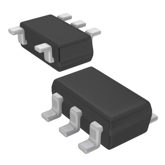
XC9141/XC9142 Series
ETR04018-002
Load Disconnection Function, 0.8A Step-up DC/DC Converters
☆GreenOperation-compatible
■GENERAL DESCRIPTION
XC9141/XC9142 series are synchronous step-up DC/DC converters with a 0.3Ω(TYP.) N-channel driver transistor and a
0.3Ω(TYP.) synchronous P-channel switching transistor built-in. A highly efficient and stable current can be supplied up to 0.8A
by reducing ON resistance of the built-in transistors.
The series are able to start operation under the condition which has 0.9V input voltage to generate 3.3V output voltage with a
100Ω load resistor, suitable for mobile equipment using only one Alkaline battery or one Nickel metal hydride battery.
The output voltage can be set from 1.8V to 5.5V (±2.0%) in steps of 0.1V.With the built-in oscillator, either 1.2MHz or 3.0MHz can
be selected for suiting to your particular application.
During the devices enter stand-by mode, A, D types prevent the application malfunction by CL Discharge Function which can
quickly discharge the electric charge at the output capacitor (CL). B, E types is able to drive RTC etc. by Bypass Switch Function
to maintain continuity between the input and output. C, F types is able to connect in parallel with other power supplies by Load
Disconnection Function which breaks continuity between the input and output.
■APPLICATIONS
■FEATURES
●Portable equipment
●Beauty & health equipment
●Wearable devices
●Game & Hobby
●PC Peripherals
●Devices with 1~3 Alkaline,
1~3 Nickel Hydride, 1 Lithium and 1 Li-ion
Input Voltage Range
Fixed Output Voltage
Oscillation Frequency
Input Current
Output Current
Control Mode Selection
Load Transient Response
Protection Circuits
Functions
Output Capacitor
Operating Ambient Temperature
Package
Environmentally Friendly
■TYPICAL APPLICATION CIRCUIT
: 0.65V~6.0V
: 1.8V~5.5V (0.1V increments)
: 1.2MHz (±15%), 3.0MHz (±20%)
: 0.8A
: 500mA @VOUT=5.0V, VBAT=3.3V (TYP.)
350mA @VOUT=3.3V, VBAT =1.8V (TYP.)
: PWM (XC9141 Series) or
Auto PWM/PFM (XC9142 Series)
: 100mV@VOUT=3.3V, VBAT =1.8V,
IOUT=1mA→200mA(tr=5μs)
: Over-current limit
Integral latch method (D,E,F type)
Output short-circuit protection (D,E,F type)
: Soft-start
Load Disconnection Function (A,C,D,F type)
CL Auto Discharge Function (A,D type)
Bypass Switch Function (B,E type)
: Ceramic Capacitor
: -40℃~+85℃
: SOT-25,USP-6C,WLP-6-01
: EU RoHS Compliant, Pb Free
■TYPICAL PERFORMANCE
CHARACTERISTICS
XC9141A33C / XC9142A33C
L=4.7μH(LQH5BPN4R7NT0L)
CIN=10μF(GRM188R60J106M),CL=10μF(GRM188R60J106M)
L=4.7μH
Lx
VOUT
100
VOUT
90
CE
CL=10μF
CE
VB AT
CIN =10μF
BAT
GND
Efficiency : EFFI [%]
80
70
60
V BAT =0.9V
V BAT =1.2V
V BAT =1.8V
V BAT =2.5V
50
40
30
20
solid line : XC9141
dotted line : XC9142
10
0
0.1
1
10
100
Output Current : IOUT [mA]
1000
1/34
�XC9141/XC9142 Series
■BLOCK DIAGRAM
●XC9141A/XC9142A type
Lx
CFB
RFB1
Error Amp.
Phase
Compensation
FB
Load disconnect
Controller
VOUT
PWM
comparator
PWM/PFM
Controller Logic
RFB2
Vref with
Soft Start
RAMP Wave
Generator
CL
Discharge
Buffer
Driver
GND
OSC
CE Controller
Logic
CE
VOUT
Current sense
VOUT
VDD
BAT
VDD MAX
* Diodes inside the circuits are ESD protection diodes and parasitic diodes.
* XC9141 series chooses only PWM control.
●XC9141B/XC9142B type
Lx
CFB
RFB1
Error Amp.
Phase
Compensation
FB
Load disconnect
Controller
VOUT
PWM
comparator
PWM/PFM
Controller Logic
RFB2
Vref with
Soft Start
RAMP Wave
Generator
Buffer
Driver
GND
OSC
CE Controller
Logic
CE
VOUT
Current sense
VOUT
VDD
Bypass SW
VDD MAX
BAT
* Diodes inside the circuits are ESD protection diodes and parasitic diodes.
* XC9141 series chooses only PWM control.
●XC9142C type
CFB
Lx
RFB1
Error Amp.
FB
Phase
Compensation
Load disconnect
Controller
Current sense
PWM/PFM
Controller Logic
Vref with
Soft Start
CE
VOUT
PWM
comparator
RFB2
RAMP Wave
Generator
Buffer
Driver
GND
OSC
CE Controller
Logic
VOUT
VDD
VDD MAX
* Diodes inside the circuits are ESD protection diodes and parasitic diodes.
2/34
VOUT
BAT
�XC9141/XC9142
Series
■BLOCK DIAGRAM (Continued)
●XC9141D/XC9142D type
Lx
CFB
RFB1
Error Amp.
Phase
Compensation
FB
PWM
comparator
PWM/PFM
Controller Logic
RFB2
Vref with
Soft Start
RAMP Wave
Generator
Load disconnect
Controller
Current sense
Short-circuit protect ion
Latch Timer
VOUT
CL
Discharge
Buffer
Driver
GND
OSC
CE Controller
Logic
CE
VOUT
VOUT
VDD
BAT
VDD MAX
* Diodes inside the circuits are ESD protection diodes and parasitic diodes.
* XC9141 series chooses only PWM control.
●XC9141E/XC9142E type
CFB
RFB1
Error Amp.
Lx
Phase
Compensation
FB
PWM
comparator
PWM/PFM
Controller Logic
RFB2
Vref with
Soft Start
RAMP Wave
Generator
Load disconnect
Controller
Current sense
Short-circuit protection
Latch Timer
VOUT
Buffer
Driver
GND
OSC
CE Controller
Logic
CE
VOUT
VOUT
VDD
Bypass SW
VDD MAX
BAT
* Diodes inside the circuits are ESD protection diodes and parasitic diodes.
* XC9141 series chooses only PWM control.
●XC9142F type
Lx
CFB
RFB1
Error Amp.
FB
Phase
Compensation
PWM
comparator
PWM/PFM
Controller Logic
RFB2
Vref with
Soft Start
CE
RAMP Wave
Generator
Load disconnect
Controller
Current sense
Short-circuit protection
Latch Timer
VOUT
VOUT
Buffer
Driver
GND
OSC
CE Controller
Logic
VOUT
VDD
VDD MAX
BAT
* Diodes inside the circuits are ESD protection diodes and parasitic diodes
3/34
�XC9141/XC9142 Series
■PRODUCT CLASSIFICATION
●Ordering Information
XC9141①②③④⑤⑥-⑦ PWM control
DESIGNATOR
ITEM
SYMBOL
DESCRIPTION
A
①
Type
B
D
Refer to Selection Guide
E
②③
④
⑤⑥-⑦(*1)
(*1)
Output Voltage
(XC9141A,B Type)
Output Voltage
(XC9141D,E Type)
Oscillation Frequency
Packages (Order Unit)
18~55
Output voltage options e.g. 1.8V → ②=1, ③=8
22~55
Output voltage options e.g. 2.2V → ②=2, ③=2
C
D
1.2MHz
3.0MHz
MR-G
SOT-25 (3,000pcs/Reel)
ER-G
USP-6C (3,000pcs/Reel)
0R-G
WLP-6-01 (5,000pcs/Reel)
The ”-G” suffix indicates that the products are Halogen and Antimony free as well as being fully EU RoHS compliant.
XC9142①②③④⑤⑥-⑦ PWM/PFM automatic switching control
DESIGNATOR
ITEM
SYMBOL
DESCRIPTION
A
B
①
Type
C
D
Refer to Selection Guide
E
F
②③
④
⑤⑥-⑦(*1)
(*1)
Output Voltage
(XC9142A,B,C Type)
Output Voltage
(XC9142D,E,F Type)
Oscillation Frequency
Packages (Order Unit)
18~55
Output voltage options e.g. 1.8V → ②=1, ③=8
22~55
Output voltage options e.g. 2.2V → ②=2, ③=2
C
1.2MHz
D
3.0MHz
MR-G
SOT-25 (3,000pcs/Reel)
ER-G
USP-6C (3,000pcs/Reel)
0R-G
WLP-6-01 (5,000pcs/Reel)
The ”-G” suffix indicates that the products are Halogen and Antimony free as well as being fully EU RoHS compliant.
4/34
�XC9141/XC9142
Series
■PRODUCT CLASSIFICATION (Continued)
●Selection guides
TYPE
OUTPUT
VOLTAGE
CHIP
ENABLE
SOFTSTART
A
Fixed
Yes
Fixed
B
Fixed
Yes
Fixed
C(*1)
Fixed
Yes
Fixed
D
Fixed
Yes
Fixed
E
Fixed
Yes
Fixed
F(*1)
Fixed
Yes
Fixed
CURRENT
LIMIT
Yes
(without latch )
Yes
(without latch )
Yes
(without latch )
Yes
(with integral latch)
Yes
(with integral latch)
Yes
(with integral latch)
SHORT
PROTECTION
WITH LATCH
CL AUTODISCHARGE
No
Yes
No
No
No
No
Yes
Yes
Yes
No
Yes
No
SHUTDOWN
OPTIONS
AT CE=L
Complete Output
Disconnect(*2)
Input-to-Output
Bypass(*2)
Complete Output
Disconnect(*3)
Complete Output
Disconnect(*2)
Input-to-Output
Bypass(*2)
Complete Output
Disconnect(*3)
(*1)
Type C,F is available for the XC9142 series only.
VOUT pin can not be connected to the different output pin such as another supply (AC adaptor).
(*3)
VOUT pin can be connected to the different output pin such as another supply (AC adaptor).
(*2)
5/34
�XC9141/XC9142 Series
■PIN CONFIGURATION
Lx
VOUT
5
4
1
CE
2
3
GND
BAT
VOUT 6
1 BAT
GND 4
Lx 5
2 GND
Lx 5
2 GND
VOUT 6
1 BAT
3 CE
GND 4
WLP-6-01
(BOTTOM VIEW)
USP-6C
(BOTTOM VIEW)
SOT-25
(TOP VIEW)
*The dissipation pad for the USP-6C package should be solder-plated in recommended mount pattern and
metal masking so as to enhance mounting strength and heat release.
If the pad needs to be connected to
other pins, it should be connected to the GND (No.2, 4) pin.
■PIN ASSIGNMENT
SOT-25
PIN NUMBER
USP-6C
WLP-6-01
1
2
3
4
5
-
3
2
1
6
5
4
3
2
1
6
5
4
PIN NAME
FUNCTIONS
CE
GND
BAT
VOUT
Lx
GND
Chip Enable
Ground
Power Input
Output Voltage
Switching
Ground
■FUNCTION CHART
PIN NAME
CE
SIGNAL
STATUS
L
Stand-by
H
Active
* Do not leave the CE pin open.
■ABSOLUTE MAXIMUM RATINGS
Ta=25℃
PARAMETER
SYMBOL
RATINGS
UNITS
BAT Pin Voltage
VBAT
-0.3~+7.0
V
Lx Pin Voltage
VLx
-0.3~+7.0
V
VOUT Pin Voltage
VOUT
-0.3~+7.0
V
CE Pin Voltage
VCE
-0.3~+7.0
V
Pd
600 (PCB mounted)
1000 (PCB mounted)
mW
Power Dissipation
SOT-25
USP-6C
WLP-6-01
700 (PCB mounted)
Operating Ambient Temperature
Topr
-40~+85
℃
Storage Temperature
Tstg
-55~+125
℃
*GND are standard voltage for all of the voltage.
6/34
3 CE
�XC9141/XC9142
Series
■ELECTRICAL CHARACTERISTICS
●XC9141/XC9142 Series
Ta=25℃
PARAMETER
SYMBOL
Input Voltage
VBAT
CONDITIONS
Voltage to start oscillation while
MIN.
TYP.
MAX.
UNITS
CIRCUIT
-
-
6.0
V
①
V
⑤
Output Voltage
VOUT
Operation Start Voltage
VST1
RL=1kΩ
-
-
0.90
V
①
Operation Hold Voltage
VHLD
RL=1kΩ
-
0.65
-
V
①
fOSC=1.2MHz
-
17.0
30.0
μA
③
fOSC=3.0MHz
-
26.0
40.0
fOSC=1.2MHz
-
1.500
fOSC=3.0MHz
-
3.000
mA
③
VBAT= VOUT(T)×0.5
fOSC=1.2MHz
1.02
1.20
1.38
IOUT=100mA
fOSC=3.0MHz
2.40
3.00
3.60
MHz
①
VBAT=1.2V,
fOSC=1.2MHz
85
93
98
VOUT= VOUT(T)-0.2V
fOSC=3.0MHz
88
93
98
%
⑤
-
-
0
%
⑤
-
165
230
mA
①
-
86(*3)
-
-
90(*3)
-
-
0.0
1.0
-
1.0
2.4
-
0.3(*2)
-
Ω
④
-
0.3(*3)
-
Ω
①
-
0.0
1.0
μA
Quiescent Current
(XC9142)
Iq
Supply Current
IDD
Oscillation Frequency
fOSC
Maximum Duty Cycle
DMAX
Minimum Duty Cycle
DMIN
PFM Switching Current
Efficiency
(XC9142)
Efficiency
IPFM
EFFI
EFFI
VOUT=VOUT(T) ×1.03→VOUT(T) ×0.97
VOUT=VBAT= VOUT(T)+0.5V
VOUT=VBAT= VOUT(T)-0.2V
VOUT=VBAT= VOUT(T)+0.5V
VBAT=1.5V,
RL is selected with VOUT(T), Refer to Table 1.
VBAT= VOUT(T)×0.6,
RL is selected with VOUT(T), Refer to Table 1.
VBAT= VOUT(T)×0.6, IOUT= 100mA
A,B,D,E
Stand-by Current
ISTB
VBAT=VLx=6.0V,VCE=0.0V
Type
(*1)
C,F Type
Lx SW "Pch" ON
Resistance
Lx SW "Nch" ON
Resistance
Lx SW”H” Leakage
Current
Lx SW”L” Leakage
Current (XC9142C/F)
Current Limit
Integral Latch Time
(D,E,F Type)
Latch Release Voltage
(D,E,F Type)
RLXP
VBAT=VLx= 6.0V, IOUT=200mA
RLXN
ILXLH
ILXLL
ILIM
to stop Lx oscillation
⑧
⑦
⑧
-
0.0
1.0
μA
②
A
⑥
fOSC=1.2MHz
45
300
725
μs
⑥
fOSC=3.0MHz
25
100
365
μs
⑥
0.9
1.2
1.5
V
①
-
VBAT(*3)
-
V
①
VBAT= VOUT(T)-0.2V, RLx=1Ω
Time from current limit start
⑦
μA
C,F Type
VBAT=0.0V,VCE=0.0V,VLx=0.0V,VOUT=6.0V
VBAT= VOUT(T)-0.2V, RLx=1Ω,
tLAT
Type
①
①
A,B,D,E
VBAT=6.0V,VCE=0.0V,
VLx=6.0V(*1)
%
After the integral latch was operated,
VLAT_R
RL is selected with VOUT(T), Refer to Table 1
VBAT=VOUT(T)-0.2V→0.9V
Short-circuit Protection
Threshold Voltage
VSHORT
VBAT=VOUT(T)-0.2V, RL=0Ω
(D,E,F Type)
7/34
�XC9141/XC9142 Series
■ELECTRICAL CHARACTERISTICS (Continued)
PARAMETER
SYMBOL
CONDITIONS
VBAT= VOUT(T)×0.6,
VOUT=VOUT(T)× 0.9,
Soft-Start Time
tSS
generated at Lx pin.
(A Type)
Bypass SW Resistance
(B Type)
0.6
1.0
2.5
fOSC=3.0MHz
0.2
0.5
1.0
UNITS
CIRCUIT
ms
⑤
VBAT= 3.3V,VOUT=3.3V,VCE=0.0V
100
180
400
Ω
②
RBSW
VBAT= 3.3V,VOUT=0.0V,VCE=0.0V
100
180
400
Ω
②
0.80
-
6.00
V
⑤
GND
-
0.20
V
⑤
VOUT= VOUT(T)-0.15V, Applied voltage to VCE,
CE ”H” Voltage
VCEH
CE ”L” Voltage
VCEL
CE ”H” Current
ICEH
VBAT=6.0V,VOUT=6.0V, VLx=6.0V, VCE=6.0V
-0.1
-
0.1
μA
②
CE ”L” Current
ICEL
VBAT=6.0V,VOUT=6.0V, VLx=6.0V, VCE=0.0V
-0.1
-
0.1
μA
②
Voltage changes Lx to be generated.
VOUT= VOUT(T)-0.15V, Applied voltage to VCE,
Voltage changes Lx to“H” level.
VOUT(T) = Target voltage
XC9141A/D,XC9142A/D,XC9142C/F type: VOUT=0V,
XC9141B/E,XC9142B/E type: VOUT=OPEN
(*2)
Design value for the XC9142C/F type.
(*3)
Designed value
Table 1. External Components RL Table
VOUT(T)
RL
UNITS:V
UNITS:Ω
1.8≦VOUT(T)
< Circuit No.④ >
V
VOUT
Lx
VOUT
Lx
A
A
BAT
BAT
CE
GND
< Circuit No.⑤ >
< Circuit No.⑥ >
Wave Form Measure Point
Wave Form Measure Point
Wave Form Measure Point
VOUT
Lx
VOUT
Lx
RLx=1Ω
RLx=56Ω
BAT
BAT
CE
GND
< Circuit No.⑧ >
VOUT
Lx
IST B
A
ILXLH
CE
GND
< Circuit No.⑦ >
A
BAT
CE
VOUT
Lx
IST B
A
GND
10/34
IOUT
CE
GND
ILXLH
A
BAT
CE
GND
�XC9141/XC9142
Series
■TYPICAL APPLICATION CIRCUIT
L
VBA T
VOUT
VOUT
Lx
BAT
CE
CE
GN D
CL
CIN
【Typical Examples】fOSC=1.2MHz
L
CL(*1)
MANUFACTURER
PRODUCT NUMBER
VALUE
murata
LQH5BPN4R7NT0L
4.7μH
TDK
LTF5022T-4R7N2R0-LC
4.7μH
Coilcraft
XFL4020-472MEC
4.7μH
murata
GRM188R60J106ME84
10μF/6.3V(*2)
murata
GRM188D71A106MA73
10μF/10V(*2)
MANUFACTURER
PRODUCT NUMBER
VALUE
TDK
LTF5022T-2R2N3R2-LC
2.2μH
Coilcraft
XFL4020-222MEC
2.2μH
murata
GRM188R60J106ME84
10μF/6.3V(*2)
murata
GRM188D71A106MA73
10μF/10V(*2)
【Typical Examples】fOSC=3.0MHz
L
CL(*1)
【Typical Examples】fOSC=1.2MHz, fOSC=3.0MHz
CIN(*1)
(*1)
MANUFACTURER
PRODUCT NUMBER
VALUE
murata
GRM188R60J106ME84
10μF/6.3V
murata
GRM188D71A106MA73
10μF/10V
Select components appropriate to the usage conditions (ambient temperature, input & output voltage).
While selecting a part, please concern about capacitance reduction and voltage durability.
(*2)
In the case of fosc=1.2MHz: If VOUT(T)≧3.5V and the load current rises above 200mA, use two or more in a parallel connection.
In the case of fosc=3.0MHz: If VBAT≧2V, VOUT(T)≧3.5V and the load current rises above 200mA, use two or more in a parallel connection.
For the actual load capacitance, use a ceramic capacitor that ensures a capacitance equivalent to or greater than the GRM188R60J106ME84
(Murata).
If using tantalum or low ESR electrolytic capacitors please be aware that ripple voltage will be higher due to the larger ESR (Equivalent Series
Resistance) values of those types of capacitors. Please also note that the IC’s operation may become unstable with such capacitors so that
we recommend to test on the board before usage.
If using electrolytic capacitor for the CL, please connect a ceramic capacitor in parallel.
11/34
�XC9141/XC9142 Series
■OPERATIONAL EXPLANATION
The XC9141/XC9142 series consists of a reference voltage source, ramp wave circuit, error amplifier, PWM comparator, phase compensation
circuit, N-channel driver transistor, P-channel synchronous rectification switching transistor and current limiter circuit.
Lx
CFB
RFB1
Error Amp.
FB
Phase
Compensation
Load disconnect
Controller
RFB2
CE
VOUT
PWM
comparator
PWM/PFM
Controller Logic
Vref with
Soft Start
VOUT
Current sense
RAMP Wave
Generator
CL
Discharge
Buffer
Driver
GND
OSC
CE Controller
Logic
VOUT
VDD
VDD MAX
Bypass SW
BAT
BLOCK DIAGRAM
The error amplifier compares the internal reference voltage with the resistors RFB1 and RFB2. Phase compensation is performed on the
resulting error amplifier output, to input a signal to the PWM comparator to determine the turn-on time of the N-channel driver transistor during
PWM operation. The PWM comparator compares, in terms of voltage level, the signal from the error amplifier with the ramp wave from the ramp
wave circuit, and delivers the resulting output to the buffer driver circuit to cause the Lx pin to output a switching duty cycle. This process is
continuously performed to ensure stable output voltage. The current feedback circuit monitors the N-channel driver transistor’s turn-on current
for each switching operation, and modulates the error amplifier output signal to provide multiple feedback signals. This enables a stable feedback
loop even when a low ESR capacitor, such as a ceramic capacitor, is used, ensuring stable output voltage.
The reference voltage forms a reference that is used to stabilize the output voltage of the IC.
After “H” level is fed to CE pin, the reference voltage connected to the error amp increases linearly during the soft start interval. This allows the
voltage divided by the internal RFB1 and RFB2 resistors and the reference voltage to be controlled in a balanced manner, and the output voltage
rises in proportion to the rise in the reference voltage. This operation prevents rush input current and enables the output voltage to rise smoothly.
The ramp wave circuit determines switching frequency. The frequency is fixed internally at 1.2MHz/3.0MHz. The Clock generated is
used to produce ramp waveforms needed for PWM operation, and to synchronize all the internal circuits.
The error amplifier is designed to monitor output voltage. The amplifier compares the reference voltage with the feedback voltage divided by
the internal resistors (RFB1 and RFB2). When the FB is lower than the reference voltage, output voltage of the error amplifier increases. The
gain and frequency characteristics of the error amplifier are optimized internally.
VDD MAX circuit compares the input voltage and the output voltage then it will select the higher one as the power supply for the IC.
The IC enters chip disable state by applying low level voltage to the CE pin. At this time, the N-channel and P-channel synchronous switching
transistors are turned OFF. With XC9142C type, the load disconnection function activates even during shutdown, and because the input voltage
VBAT and output voltage VOUT are compared to optimally control the orientation of the parasitic diode of the P-channel synchronous switching
transistor, a parallel connection with other power supplies is possible. With the XC9141 series and XC9142A/B types, the orientation of the
parasitic diode of the P-channel synchronous switching transistor is fixed at anode: VOUT and cathode: Lx during shutdown to break conduction
from the input side to the output side by the parasitic diode of the P-channel synchronous switching transistor.
When PFM operates, the N-channel driver transistor turns on at the timing of the signal sent from the PWM comparator. The N-channel driver
transistor remains on until the current in the coil reaches a constant current (IPFM). The PWM/PFM control circuit compares the signal sent from
the PWM comparator to the time it takes the current in the coil to reach a constant current (IPFM), and outputs the pulse that results in a longer ontime of the N-channel driver transistor. This enables smooth switching between PWM and PFM. The XC9141 series directly outputs the signal
that is sent from the PWM comparator.
12/34
�XC9141/XC9142
Series
■OPERATIONAL EXPLANATION (Continued)
The maximum current limit function of XC9141A/B types and XC9142A/B/C types constantly monitors the current flowing in the N-channel driver
transistor connected to the Lx pin, and if the current in the N-channel driver transistor exceeds the current limit, the function turns off the N-channel
driver transistor. (Please refer to Fig. ILIM①)
① If the current flowing in the N-channel driver transistor exceeds the current limit value (equivalent to the peak coil current), the N-channel
driver transistor turns off, and remains off during the clock interval.
② At the next clock, the N-channel driver transistor turns on.
If overcurrent continues, ① and ② are repeated.
Note that the current in the internal N-channel driver transistor is not the same as the output current IOUT.
tSS
VOUT(T)
VBAT
VOUT
ILIM
ILx
RL
CE
①②
①②
Fig. ILIM
The maximum current limit function of XC9141D/E and XC9142D/E/F types monitors the current that flows in the N-channel driver transistor
connected to the Lx pin, and consists of both maximum current limiting and a latch function. (Please refer to Fig.ILIM②)
Short-circuit protection is a latch-stop function that activates when the output voltage drops below the short-circuit protection threshold voltage in
the overcurrent state. (Please refer to Fig.ILIM③)
① If the current flowing in the N-channel driver transistor exceeds the current limit value (equivalent to the peak coil current), the N-channel
driver transistor turns off, and remains off during the clock interval. In addition, an integral latch timer starts the count.
② The N-channel driver transistor turns on at the next pulse. If in the overcurrent state at this time, the N-channel driver transistor turns off as
in (1). The integral latch timer continues the count.
③ If the count of the integral latch timer continues for 300μs typ.(@fosc=1.2MHz), a function that latches the N-channel driver transistor and Pchannel synchronous switching transistor to the off state activates.
④ If no longer in the overcurrent state at the next pulse, normal operation resumes. The integral latch timer stops the count.
⑤
⑥
⑦
If the output voltage VOUT drops below the short-circuit protection threshold voltage VSHORT during the count of the integral latch timer, a
function that latches the N-channel driver transistor and P-channel synchronous switching transistor in the off state activates. The shortcircuit protection threshold voltage VSHORT is a threshold voltage that is linked to the input voltage VBAT.
In the latched state, either restart by shutting down once with the CE pin, or resume operation by lowering the input voltage VBAT below the
latch release voltage VLAT_R(1.2V typ.). The soft start function operates during restart. During the soft-start interval tSS, the integral latch timer
and latch function are stopped.
When the input voltage VBAT is below the latch release voltage VLAT_R(1.2V typ.), the integral latch timer and latch function stop, but the current
limiting function continues operating.
* Note that the current in the internal N-channel driver transistor is not the same as the output current IOUT.
VOUT
VBAT
Limit


 工商网监
湘ICP备2023018690号
工商网监
湘ICP备2023018690号
