TC78H670FTG
TOSHIBA CD process Integrated Circuit Silicon Monolithic
TC78H670FTG
Clock-in and Serial controlled Bipolar Stepping Motor Driver
1. Outline
The TC78H670FTG is a two-phase bipolar stepping motor driver using a PWM
chopper which incorporate DMOS with low on-resistance in output
transistors. The clock-in decoder is built in.
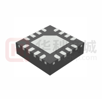
P-VQFN16-0303-0.50-001
Weight: 22.9 mg (typ.)
2. Features
•
Built-in Dual H Bridges, Capable of controlling 1 bipolar stepping motor
•
PWM controlled constant-current drive
•
Power supply operating voltage: 2.5 V to 16.0 V
•
Output current ratings: 2.0 A (max)
•
Low on-resistance (High + Low side = 0.48 Ω (typ.)) MOSFET output stage
•
Allows full, half, quarter, 1/8, 1/16, 1/32, 1/64, 1/128 step operation
•
Built-in Sense resistor less current control architecture (Advanced Current Detection System)
•
Multi error detect functions (Thermal shutdown (TSD), Over current (ISD), motor load open (OPD)
and Under voltage lockout(UVLO))
•
Error detection (TSD/ISD/OPD) flag output function
•
Built-in VCC regulator for internal circuit
•
Chopping frequency of a motor can be adjusted by external resistor
•
Small QFN package with thermal pad (16pin)
Note: Please be careful about thermal conditions during using.
Note: It is possible to detect OPD only when Serial mode is selected.
Start of commercial production
2020-01
© 2019-2020
Toshiba Electronic Devices & Storage Corporation
1
2020-07-02
�TC78H670FTG
3. Pin Assignment
(Top View)
MODE2 /
CLK /
S_CLK
MODE1 /
SET_EN /
LATCH
15
16
MODE0 /
UP-DW /
EN / ERR
S_DATA
14
13
MODE3 / CW-CCW
1
12
STBY
AGND
2
11
OSCM
VM
3
10
VREF
4
9
PGND_B
TC78H670FTG
PGND_A
5
OUT_A+
6
7
OUT_A- OUT_B-
8
OUT_B+
Note: Please solder the corner pads and the rear thermal pad of the QFN package, to the GND pattern of the PCB.
2
2020-07-02
�TC78H670FTG
4. Pin Description
Pin No.
STBY = Low
1
STBY = High
Pin description
CLK-IN mode
Serial mode
MODE3
CW-CCW
—
MODE3: Step mode select pin
CW-CCW: Current direction setup pin
2
AGND
←
←
GND pin
3
VM
←
←
Motor power supply input pin
4
PGND_A
←
←
Ach Power GND pin
5
OUT_A+
←
←
A channel motor output(+) pin
6
OUT_A-
←
←
A channel motor output(-) pin
7
OUT_B-
←
←
B channel motor output(-) pin
8
OUT_B+
←
←
B channel motor output(+) pin
9
PGND_B
←
←
Bch Power GND pin
10
VREF
←
←
Current threshold reference pin
11
OSCM
←
←
Internal oscillator frequency setting pin
12
STBY
←
←
Standby pin
13
EN/ERR
←
←
Enable(Motor output ON/OFF) pin /
Error detection flag output pin
14
MODE0
UP-DW
S_DATA
15
MODE1
SET_EN
LATCH
MODE1: Step mode select pin
SET_EN: Step mode setting enable pin
LATCH: Latch enable pin
16
MODE2
CLK
S_CLK
MODE2: Step mode select pin
CLK:
Step Clock input pin
S_CLK: Serial clock input pin
3
MODE0: Step mode select pin
UP-DW: Step mode setting pin
S_DATA: Serial data input pin
2020-07-02
�TC78H670FTG
5. Block Diagram
VM
AGND
STBY
INBuff
STBY
Control
Regulator
UVLO
VREF
GAIN
OSC
VREF
OUT_A+
Predriver
H Bridge
ISD
MODE3 / CW-CCW
INBuff
OUT_A-
DAC
MODE2 / CLK / S_CLK
INBuff
DET_
COMP
SENS_
ILEVEL
PGND_A
MODE1 / SET_EN / LATCH
INBuff
OPD
Control
Logic
MODE0 / UP-DW / S_DATA
TSD
INBuff
OUT_B+
EN / ERR
IOBuff
OSCM
OSCM
Predriver
ISD
H Bridge
OUT_B-
DAC
DET_
COMP
SENS_
ILEVEL
PGND_B
Note:
Some of the functional blocks, circuits, or constants in the block diagram may be omitted or simplified for
explanatory purpose.
Note:
All the grounding wires should be solid patterns and be externally terminated at only one point. Also, a
grounding method should be considered for efficient heat dissipation. Careful attention should be paid to the
layout of the output, VM and GND traces, to avoid short circuits across output pins or to the power supply or
ground. If such a short circuit occurs, the device may be permanently damaged. Also, the utmost care should
be taken for pattern designing and implementation of the device since it has power supply pins (VM, AGND,
PGND_x, OUT_x+ and OUT_x- (x = A or B)) through which a particularly large current may run. If these pins
are wired incorrectly, an operation error may occur or the device may be destroyed. The logic input pins must
also be wired correctly. Otherwise, the device may be damaged owing to a current running through the IC that
is larger than the specified current. Careful attention should be paid to design patterns and mounting.
4
2020-07-02
�TC78H670FTG
6. Input / Output Equivalent Circuit
Pin name
MODE3 / CW-CCW
MODE2 / CLK / S_CLK
MODE1 / SET_EN / LATCH
MODE0 / UP-DW / S_DATA
STBY
Equivalent circuit
MODE3 / CW-CCW
MODE2 / CLK / S_CLK
MODE1 / SET_EN / LATCH
MODE0 / UP-DW / S_DATA
STBY
EN / ERR
EN / ERR
VREF
VREF
OSCM
OSCM
VM
OUT_A+
OUT_AOUT_B+
OUT_BPGND_A
PGND_B
OUT_x+
OUT_x-
X=A or B
PGND_x
Note: The equivalent circuit diagrams may be simplified for explanatory purposes.
5
2020-07-02
�TC78H670FTG
7. Control Mode Select Function
The MODE0-3 pins set Serial mode or CLK-IN mode.
The control mode is set up by the input state of the MODE0-3 pins after releasing standby mode.
MODE3
pin input
MODE2
pin input
MODE1
pin input
MODE0
pin input
L
L
L
L
Function
Serial mode
Other than the above
CLK-IN mode
VM
tmodeho
tmodeho
tmodesu
tmodesu
H
STBY
L
H
MODE0
L
H
MODE1
L
H
MODE2
L
H
MODE3
L
Control Mode
Setting
Non
operation
CLK-IN mode
Non
operation
Serial mode
Characteristics
Symbol
Test condition
Min
Typ.
Max
Unit
Mode setting
Setup time
tmodesu
To STBY edge
1
—
—
μs
Mode setting
Data hold time
tmodeho
From STBY edge
100
—
—
μs
6
2020-07-02
�TC78H670FTG
8. Functional Description 1 (for CLK-IN mode)
CLK Function
Each up-edge of the CLK signal will shift the motor’s electrical angle per step.
CLK pin input
Function
Up-edge
Shifts the electrical angle per step
Down-edge
(State of the electrical angle does not change)
ENABLE Function
The EN pin controls the ON and OFF of the stepping motor outputs. Motor operation starts and stops by setting H and L
to the EN pin. (When EN pin is set to L (OFF), all of the MOSFETs turn off and become high impedance (hereafter, Hi-Z).)
Setting the EN pin to L, and avoiding the motor to operate during VM power-on and power-off (i.e., outside of the operating
voltage range) is recommended. Then, switch the EN pin to H after the VM reaches the target voltage and becomes stable.
EN pin input
Function
L
OFF (Hi-Z)
H
ON (Normal operation mode)
VM
H
STBY
L
H
EN
L
Internal processing time
200μs(Reference value)
CW-CCW Function
CW-CCW pin controls the rotation direction of the motor.
CW-CCW pin input
Function
L
Counter clockwise operation (CCW)
H
Clockwise operation (CW)
7
2020-07-02
�TC78H670FTG
Step Resolution Select Function
Step resolution is set up. TC78H670FTG has the two modes, Variable Mode and Fixed Mode. These modes are set up by
the input state of MODE0-3 pins after releasing standby mode.
Variable Mode: Variable mode can be started with Full step resolution and changed step resolution during
motor operating
Fixed Mode:
Fixed mode can be started with the mode user selected and continued it during motor operating
MODE3
pin input
MODE2
pin input
MODE1
pin input
MODE0
pin input
L
L
L
H
Full step resolution 1/2 step resolution
(2-phase excitation) (1-2-phase excitation)
L
L
H
L
Full step resolution 1/4 step resolution
(2-phase excitation) (W1-2-phase excitation)
L
L
H
H
Full step resolution 1/8 step resolution
(2-phase excitation) (2W1-2-phase excitation)
L
H
L
L
L
H
L
H
Full step resolution 1/32 step resolution
(2-phase excitation) (8W1-2-phase excitation)
L
H
H
L
Full step resolution 1/64 step resolution
(2-phase excitation) (16W1-2-phase excitation)
L
H
H
H
Full step resolution 1/128 step resolution
(2-phase excitation) (32W1-2-phase excitation)
H
L
L
L
Full step resolution (2-phase excitation)
H
L
L
H
1/2 step resolution (1-2-phase excitation)
H
L
H
L
1/4 step resolution (W1-2-phase excitation)
H
L
H
H
H
H
L
L
H
H
L
H
1/32 step resolution (8W1-2-phase excitation)
H
H
H
L
1/64 step resolution (16W1-2-phase excitation)
H
H
H
H
1/128 step resolution (32W1-2-phase excitation)
Mode
Variable Mode
Fixed Mode
8
Function
Full step resolution 1/16 step resolution
(2-phase excitation) (4W1-2-phase excitation)
1/8 step resolution (2W1-2-phase excitation)
1/16 step resolution (4W1-2-phase excitation)
2020-07-02
�TC78H670FTG
When Step mode is changed during operating, Step resolution can be set by SET_EN pin and UP-DW pin.
Step mode is changed synchronously with Step Clock.
SET_EN pin input
Function
L
Setting step mode is invalid
H
Setting step mode is available
UP-DW pin input
Function
L
Change step mode to high resolution
H
Change step mode to Low resolution
[Example: Full Step 1/8 Step]
EN
SET_EN
H
L
H
L
UP-DW
H
L
H
CLK
L
Step setting
1/1
1/2
1/4
1/8
9
1/4
2020-07-02
�TC78H670FTG
Timing Chart of Step Resolution Setting and Initial Angle
The arrow in the below figures indicates the timing of initial angle.
[Full step resolution]
CLK
H
L
+100%
Iout (A)
0%
-100%
+100%
Iout (B)
0%
-100%
CCW
CW
[1/2 step resolution]
CLK
H
L
+100%
+71%
Iout (A)
0%
-71%
-100%
+100%
+71%
Iout (B)
0%
-71%
-100%
CCW
CW
Note: Timing charts may be simplified for explanatory purpose.
10
2020-07-02
�TC78H670FTG
[1/4 step resolution]
H
CLK
L
+100%
+92%
+71%
+38%
Iout (A) 0%
-38%
-71%
-92%
-100%
+100%
+92%
+71%
+38%
Iout (B) 0%
-38%
-71%
-92%
-100%
CCW
CW
Note: Timing charts may be simplified for explanatory purpose.
11
2020-07-02
�TC78H670FTG
[1/8 step resolution]
CLK
H
L
+100%
+98%
+92%
+83%
+71%
+56%
+38%
+20%
Iout (A)
0%
-20%
-38%
-56%
-71%
-83%
-92%
-98%
-100%
+100%
+98%
+92%
+83%
+71%
+56%
+38%
+20%
Iout (B)
0%
-20%
-38%
-56%
-71%
-83%
-92%
-98%
-100%
CCW
CW
Note: Timing charts may be simplified for explanatory purpose.
12
2020-07-02
�TC78H670FTG
[1/16 step resolution]
H
L
CLK
+100%
+98%
+92%
+83%
+71%
+56%
+38%
+20%
Iout (A)
0%
-20%
-38%
-56%
-71%
-83%
-92%
-98%
-100%
+100%
+98%
+92%
+83%
+71%
+56%
+38%
+20%
Iout (B)
0%
-20%
-38%
-56%
-71%
-83%
-92%
-98%
-100%
CCW
CW
Note: Timing charts may be simplified for explanatory purpose.
13
2020-07-02
�TC78H670FTG
Step Setting and Current Percentage
Current (%)
1/1
1/2
1/4
1/8
1/16
1/32
1/64
1/128
100%
○
○
○
○
○
○
○
○
○
○
○
○
○
○
○
○
○
○
○
○
○
○
○
○
○
○
○
○
○
○
○
○
○
○
○
○
○
○
○
○
○
○
○
○
99%
○
98%
97%
○
96%
95%
○
94%
93%
○
92%
91%
○
90%
89%
○
○
88%
87%
○
86%
○
85%
84%
○
83%
○
○
82%
○
80%
79%
○
○
○
○
○
○
○
○
78%
○
77%
○
76%
○
○
○
○
○
75%
○
74%
○
○
○
73%
71%
○
○
○
81%
72%
○
○
○
○
○
○
○
○
○
○
○
70%
○
69%
○
○
68%
○
67%
○
○
○
66%
○
65%
○
○
64%
○
63%
○
62%
○
○
○
○
○
61%
○
60%
○
○
○
59%
○
58%
○
○
57%
○
56%
○
○
○
○
○
55%
○
53%
○
52%
14
○
○
2020-07-02
�TC78H670FTG
Current (%)
1/1
1/2
1/4
1/8
1/16
1/32
51%
○
○
○
49%
○
○
48%
○
47%
○
○
○
○
46%
○
45%
○
○
44%
○
43%
○
○
○
42%
○
41%
○
○
39%
○
38%
○
○
○
○
○
○
37%
○
36%
○
○
35%
○
34%
○
○
○
33%
○
31%
○
○
30%
○
29%
○
○
○
○
28%
○
27%
○
25%
○
○
○
24%
○
○
23%
○
22%
○
○
21%
○
20%
○
○
○
○
○
18%
○
17%
○
○
16%
○
15%
○
○
○
13%
○
12%
○
○
11%
○
10%
○
○
○
○
9%
○
7%
○
○
6%
○
5%
○
○
○
4%
○
2%
0%
1/128
○
50%
1%
1/64
○
○
○
○
○
15
○
○
○
○
2020-07-02
�TC78H670FTG
Step Resolution and Set Current
STEP
1/128
Ach
Bch
(%)
(%)
1/64
Ach
Bch
(%)
(%)
1/32
Ach
Bch
(%)
(%)
1/16
Ach
Bch
(%)
(%)
Ach
(%)
Bch
(%)
Ach
(%)
Bch
(%)
Ach
(%)
Bch
(%)
θ0
100
0
100
0
100
0
100
0
100
0
100
0
100
0
θ1
100
1
θ2
100
2
100
2
θ3
100
4
θ4
100
5
100
5
100
5
θ5
100
6
θ6
100
7
100
7
θ7
100
9
θ8
100
10
100
10
100
10
100
10
99
12
99
15
99
15
99
17
98
20
98
20
98
20
98
20
98
22
97
24
97
24
96
27
96
29
96
29
96
29
95
31
94
34
94
34
93
36
92
38
92
38
92
38
92
38
92
38
91
41
90
43
90
43
89
45
88
47
88
47
88
47
—
θ9
99
11
θ10
99
12
θ11
99
13
θ12
99
15
θ13
99
16
θ14
99
17
θ15
98
18
θ16
98
20
θ17
98
21
θ18
98
22
θ19
97
23
θ20
97
24
θ21
97
25
θ22
96
27
θ23
96
28
θ24
96
29
θ25
95
30
θ26
95
31
θ27
95
33
θ28
94
34
θ29
94
35
θ30
93
36
θ31
93
37
θ32
92
38
θ33
92
39
θ34
91
41
θ35
91
42
θ36
90
43
θ37
90
44
θ38
89
45
θ39
89
46
θ40
88
47
θ41
88
48
16
1/8
1/4
1/2
Full
Ach
(%)
Bch
(%)
2020-07-02
�TC78H670FTG
STEP
1/128
Ach
Bch
(%)
(%)
1/64
Ach
Bch
(%)
(%)
θ42
87
49
87
49
θ43
86
50
θ44
86
51
86
51
θ45
85
52
θ46
84
53
84
53
θ47
84
55
θ48
83
56
83
56
θ49
82
57
θ50
82
58
82
58
θ51
81
59
θ52
80
60
80
60
θ53
80
61
θ54
79
62
79
62
θ55
78
62
θ56
77
63
77
63
θ57
77
64
θ58
76
65
76
65
θ59
75
66
θ60
74
67
74
67
θ61
73
68
θ62
72
69
72
69
θ63
72
70
θ64
71
71
71
71
θ65
70
72
θ66
69
72
69
72
θ67
68
73
θ68
67
74
67
74
θ69
66
75
θ70
65
76
65
76
θ71
64
77
θ72
63
77
63
77
θ73
62
78
θ74
62
79
62
79
θ75
61
80
θ76
60
80
60
80
θ77
59
81
θ78
58
82
58
82
θ79
57
82
θ80
56
83
56
83
θ81
55
84
θ82
53
84
53
84
θ83
52
85
θ84
51
86
51
86
θ85
50
86
—
1/32
Ach
Bch
(%)
(%)
86
51
83
56
80
60
77
63
74
67
71
71
67
74
63
77
60
80
56
83
51
86
1/16
Ach
Bch
(%)
(%)
Ach
(%)
Bch
(%)
83
56
83
56
77
63
71
71
71
71
63
77
56
83
56
83
17
1/8
1/4
1/2
Full
Ach
(%)
Bch
(%)
Ach
(%)
Bch
(%)
Ach
(%)
Bch
(%)
71
71
71
71
100
100
2020-07-02
�TC78H670FTG
STEP
1/128
Ach
Bch
(%)
(%)
1/64
Ach
Bch
(%)
(%)
θ86
49
87
49
87
θ87
48
88
θ88
47
88
47
88
θ89
46
89
θ90
45
89
45
89
θ91
44
90
θ92
43
90
43
90
θ93
42
91
θ94
41
91
41
91
θ95
39
92
θ96
38
92
38
92
θ97
37
93
θ98
36
93
36
93
θ99
35
94
θ100
34
94
34
94
θ101
33
95
θ102
31
95
31
95
θ103
30
95
θ104
29
96
29
96
θ105
28
96
θ106
27
96
27
96
θ107
25
97
θ108
24
97
24
97
θ109
23
97
θ110
22
98
22
98
θ111
21
98
θ112
20
98
20
98
θ113
18
98
θ114
17
99
17
99
θ115
16
99
θ116
15
99
15
99
θ117
13
99
θ118
12
99
12
99
θ119
11
99
θ120
10
100
10
100
θ121
9
100
θ122
7
100
7
100
θ123
6
100
θ124
5
100
5
100
θ125
4
100
θ126
2
100
2
100
θ127
1
100
θ128
0
100
0
100
—
1/32
Ach
Bch
(%)
(%)
1/16
Ach
Bch
(%)
(%)
47
88
47
88
43
90
38
92
38
92
34
94
29
96
29
96
24
97
20
98
20
98
15
99
10
100
10
100
5
100
0
100
0
100
18
1/8
1/4
1/2
Ach
(%)
Bch
(%)
Ach
(%)
Bch
(%)
38
92
38
92
20
98
0
100
0
100
Full
Ach
(%)
Bch
(%)
0
100
Ach
(%)
Bch
(%)
2020-07-02
�TC78H670FTG
9. Functional Description 2 (for Serial mode)
Under the serial mode, it performs setting and motor control in the following 32 bit format.
For the motor control, each current value is set in the serial setting, and the output is updated to the set current value at
the timing of the LATCH signal.
S_CLK
S_DATA
LATCH
D0
D1
D2
D3
D4
D5
D6
D7
D8
D9
D10
D11
D12
D13
D14
D15
MDT
_A0
MDT
_A1
PHA
CA0
CA1
CA2
CA3
CA4
CA5
CA6
CA7
CA8
CA9
—
—
—
D16
D17
D18
D19
D20
D21
D22
D23
D24
D25
D26
D27
D28
D29
D30
D31
MDT
_B0
MDT
_B1
PHB
CB0
CB1
CB2
CB3
CB4
CB5
CB6
CB7
CB8
CB9
TRQ
0
TRQ
1
OPD
Note: Every issuing a command, the current setting transfers by one step.
19
2020-07-02
�TC78H670FTG
Register
The registers to use the serial control are shown below.
9.1.1. PHx (x = A or B)
The polality of the output current can be selected by PHx registers for each channel.
PHx
L
Function
Setting the direction of the output current to minus
H
* Default
Setting the direction of the output current to plus
9.1.2. Cx0 to Cx9 (x = A or B)
The output of each channel’s DAC for current limitation can be set by Cx0 to Cx9 registers.
The relation between Setting DAC and the output current (Iout) are shown below.
Iout (Max) = Vref (V) ×
Cx[9:0]
1023
× Setting torque by the torque function (%)
9.1.3. TRQ0 and TRQ1
The value of the motor torque can be set by TRQ0 and TRQ1 registers.
TRQ1
TORQ0
Function
L
L
L
H
Torque setting: 75%
H
L
Torque setting: 50%
H
H
Torque setting: 25%
Torque setting: 100%
* Default
9.1.4. OPD
An ON/OFF of the open detection function of motor output pins can be switched by OPD register.
OPD
L
H
Function
Open detection OFF
* Default
Open detection ON
20
2020-07-02
�TC78H670FTG
9.1.5. Selectable Mixed Decay Function MDT_x0 and MDT_x1 (x = A or B)
The Selectable Mixed Decay can adjust the current regeneration amount during the period of current regeneration. Though
the Mixed Decay is determined by controlling 2 different types of Decay (Fast Decay and Slow Decay), this function enables
the user to select the ratio of the Mixed Decay using MDT_x0 and MDT_x1 register.
MDT_x1
MDT_x0
Function
L
L
L
H
Fast Decay: 75%
H
L
Fast Decay: 50%
H
H
Fast Decay only
Fast Decay: 37.5% (Fast Decay = OSCM × 6)
* Default
fchop
OSCM internal
signal
Setting current
(NFth)
NF detection
(MDT_x1/MDT_x0) = (L/L): Fast Decay 37.5%
(MDT_x1/MDT_x0) = (L/H): Fast Decay: 75%
(MDT_x1/MDT_x0) = (H/L): Fast Decay 50%
(MDT_x1/MDT_x0) = (H/H): Fast Decay only
Charge Mode -> NF detect -> Slow Decay -> Fast Decay -> 1 fchop cycle ->Charge Mode
1fchop cycle: OSCM × 16 clock
Note: x = A or B
Note: Decay control is controlled in order of Charge, Slow Decay and Fast Decay.
Note: The blanking time(AtBLK) is also set to prevent an incorrect operation in the NF detection (the motor current
reaches the set current value (NFth))..
Note: Timing charts may be simplified for explanatory purpose.
21
2020-07-02
�TC78H670FTG
Mixed Decay Waveform (Current Waveform) *Charge → Slow Decay → Fast Decay
fchop
fchop
OSCM internal
signal
NF Detection
NF Detection
Setting
current
Iout
Charge
Slow Decay
Fast Decay
Note: Timing charts may be simplified for explanatory purpose.
22
2020-07-02
�TC78H670FTG
Constant Current PWM Function and Timings *Charge → Slow Decay → Fast Decay
OSCM
Internal
signal
OSCM
Internal
signal
MDT setting
MDT setting
NF detection
NF detection
Setting
current
Setting
current
Iout
Iout
Charge
Slow Decay
Fast Decay
Charge
Slow
Decay
Fast Decay
fchop
fchop
If the NF is detected during the early timing of the
fchop cycle, the Slow Decay will be longer.
If the NF is detected during the late timing of the
fchop cycle, the Slow Decay will be shorter.
The Charge period (the time until the motor current reaches the set current value) is determined by the operating status.
Therefore the NF detection timing (the motor current reaches the set current value) with the chopping cycle (fchop) may
change. If NF is detected in the early period of the fchop cycle, the Slow Decay will be longer. If NF is detected in the late
period of the fchop cycle, the Slow Decay will be shorter, as shown above.
Note:
The chopping cycle is determined as: fchop - (Charge + Fast Decay) = Slow Decay
(Fast Decay ratio can be changed by MDT_x0 and MDT_x1 (x = A or B) registers setting.)
OSCM
Internal
signal
MDT setting
NF detection
Setting
current
Iout
Charge
Fast
Decay
fchop
If NF is detected within the MDT setting, Decay
sequence will only be Fast Decay.(Slow Decay
does not appear.)
Note: Timing charts may be simplified for explanatory purpose.
23
2020-07-02
�TC78H670FTG
Mixed Decay current waveform *Charge → Slow Decay → Fast Decay
When the next current step is higher:
fchop
fchop
fchop
fchop
OSCM
Internal
signal
NF
NF
Setting
current
Slow
Fast
Setting
current
NF
Fast
Charge
NF
Slow
Slow
Charge
Fast
Slow
Charge
Fast
Charge
When Charge Period is More Than 1 fchop Cycle:
When the Charge period is longer than fchop cycle, the Charge period extends until the motor current reaches the NF
threshold. Once the current reaches the next current step, then the sequence goes on to Decay mode.
fchop
fchop
fchop
fchop
OSCM
Internal
signal
NF
Setting
current
Slow
Fast
Charge
Setting
current
NF
NF
Slow
Charge
•
Fast
Charge
Slow
Fast
When the Next Current Step is lower:
fchop
fchop
fchop
fchop
OSCM
Internal
signal
Charge mode will appear per each fchop cycle to check the
current level using RS comparator. If the current level is
Setting
current
NF
switched to Slow Decay in a very short period.
Slow
Slow
Charge
already above the current set level, the sequence will be
NF
Fast
Charge
NF
Fast
Charge
Setting
current
Slow
NF
Fast
Charge
Slow
Fast
Note: Timing charts may be simplified for explanatory purpose.
24
2020-07-02
�TC78H670FTG
Serial Setting Example when driving a motor
Serial setting example for motor operation is shown below.
The motor operates with full step resolution by transmitting from the 1st to 4th commands repeatedly.
1st Command
D0
D1
D2
D3
D4
D5
D6
D7
D8
D9
D10
D11
D12
D13
D14
D15
0
0
1
1
1
1
1
1
1
1
1
1
1
0
0
0
D16
D17
D18
D19
D20
D21
D22
D23
D24
D25
D26
D27
D28
D29
D30
D31
0
0
1
1
1
1
1
1
1
1
1
1
1
0
0
0
2nd Command
D0
D1
D2
D3
D4
D5
D6
D7
D8
D9
D10
D11
D12
D13
D14
D15
0
0
0
1
1
1
1
1
1
1
1
1
1
0
0
0
D16
D17
D18
D19
D20
D21
D22
D23
D24
D25
D26
D27
D28
D29
D30
D31
0
0
1
1
1
1
1
1
1
1
1
1
1
0
0
0
3rd Command
D0
D1
D2
D3
D4
D5
D6
D7
D8
D9
D10
D11
D12
D13
D14
D15
0
0
0
1
1
1
1
1
1
1
1
1
1
0
0
0
D16
D17
D18
D19
D20
D21
D22
D23
D24
D25
D26
D27
D28
D29
D30
D31
0
0
0
1
1
1
1
1
1
1
1
1
1
0
0
0
4th Command
D0
D1
D2
D3
D4
D5
D6
D7
D8
D9
D10
D11
D12
D13
D14
D15
0
0
1
1
1
1
1
1
1
1
1
1
1
0
0
0
D16
D17
D18
D19
D20
D21
D22
D23
D24
D25
D26
D27
D28
D29
D30
D31
0
0
0
1
1
1
1
1
1
1
1
1
1
0
0
0
25
2020-07-02
�TC78H670FTG
10. Common Function (CLK-IN Mode and Serial Mode)
Error Function (Error detect flag output)
When TC78H670FTG detects some errors, ERR pin outputs low level to peripheral block.
Since ERR pin and EN pin share the function, the below peripheral circuit between TC78H670FTG and HOST MCU
should be inserted. In normal status, since the internal MOSFET is OFF, the level of ERR pin is equal to the MODE
control voltage from outside. When the error function (Thermal shutdown (TSD), Over current (ISD), or motor load
open (OPD)) occurs, ERR pin will become Low (the internal MOSFET is ON). When the error detection is released
by reasserting the VM power supply or setting the device to STANDBY mode, ERR pins show “normal status”.
TC78H670FTG
HOST MCU
EN
EN/ERR
TSD
ISD
OPD
ERR
Note: This figure may be simplified for explanatory purpose.
Note: It is possible to detect OPD only when Serial mode is selected.
ERR pin output
Function
H
Normal status (Normal operation)
L
Detect error status (ISD, TSD, OPD)
After detecting TSD detection: TC78H670FTG draws out currents of motor by Fast mode. If the output current is zerodetected or for 1ms at maximum, the output becomes Hi-Z.
After detecting ISD detection: In H Bridge high-side (Pch DMOS) detection, TC78H670FTG draws out currents of motor
by Slow mode on low-side. The output after 80 ms (typ.) becomes Hi-Z. In H Bridge low-side (Nch DMOS) detection, it
draws out by Slow mode on high-side.
Note: Above times are reference values, and are not guaranteed.
26
2020-07-02
�TC78H670FTG
STANDBY Function
It is possible to switch to Standby mode by STBY pin.
STBY pin input
Function
MEMO
L
Standby mode
Electrical angle: 45°
H
Normal operation
—
Note: When STBY pin is Low, TC78H670FTG stops supplying the power to logic circuit.
Therefore, Logic circuit is reset and Electrical angle and Step mode are initialized.
H
STBY
L
1ms at maximum (Reference value)
Output current
Internal processing time
100μs(Reference value)
Mode
Normal mode
27
Standby mode
2020-07-02
�TC78H670FTG
11. Output Transistor Function Mode
VM
VM
U1
ON
VM
U2
U1
U2
OFF
OFF
OFF
OUT_xOUT_x+
OUT_x-
OUT_x+
U2
U1
OFF
ON
OUT_x+
Load
Load
L1
OFF
Load
OUT_x-
L2
L1
L2
L1
L2
ON
ON
ON
ON
OFF
PGND_x
PGND_x
PGND_x
x = A or B
Charge mode
A current flows into the
motor coil.
Note:
Slow mode
A current circulates around
the motor coil and this device.
Fast mode
The energy of the motor coil
is fed back to the power.
The equivalent circuit diagrams may be simplified or some parts of them may be omitted for explanatory
purposes.
Output Transistor Function
MODE
U1
U2
L1
L2
Charge
ON
OFF
OFF
ON
Slow
OFF
OFF
ON
ON
Fast
OFF
ON
ON
OFF
Note:
This table shows an example of when the current flows as indicated by the arrows in the figures shown above.
If the current flows in the opposite direction, refer to the following table.
MODE
U1
U2
L1
L2
Charge
OFF
ON
ON
OFF
Slow
OFF
OFF
ON
ON
Fast
ON
OFF
OFF
ON
This IC controls the motor current to be constant by changing 3 modes listed above automatically
Note: To eliminate shoot-through current that flows from supply to ground due to the simultaneous conduction of high
side and low side transistors in the bridge output, a dead time (100ns (Reference value)) is generated in this IC when
transistors switch from on to off, or vice versa.
28
2020-07-02
�TC78H670FTG
12. Calculation of the Predefined Output Current
The peak output current (Setting current value) can be set via the reference voltage (Vref), as follows:
Iout (Max) = 1.1 × Vref (V)
13. OSCM Oscillation Frequency and Chopping Frequency
The OSCM oscillation frequency (fOSCM) and chopping frequency (fchop) can be adjusted by the external resistor (ROSC)
connecting to OSCM pin.
ROSC[kΩ]
fOSCM [kHz](typ.)
fchop[kHz](typ.)
18
3290
206
22
2691
168
30
1982
124
39
1526
95
47
1266
79
56
1064
66
75
795
50
91
656
41
If chopping frequency is raised, ripple of current will become small and wave-like reproducibility will improve.
However, the gate loss inside IC goes up and generation of heat becomes large.
By lowering chopping frequency, reduction in generation of heat is expectable. However, ripple of current may become
large.
It is a standard about 70 kHz. A setup in the range of 50 kHz to 100 kHz is recommended.
29
2020-07-02
�TC78H670FTG
14. Absolute Maximum Ratings (Ta = 25°C)
Characteristics
Rating
Unit
Remarks
20
V
Outputs are OFF
18
V
Outputs are ON
20
V
STBY pin = L
-0.4 to 18
V
STBY pin = H
Iout
2.0
A
(Note 1)
VIN(H)
6.0
V
—
VIN(L)
-0.4
V
—
ERR output pin voltage
VLO
6.0
V
—
ERR output pin inflow current
ILO
6.0
mA
—
Power dissipation
PD
1.79
W
(Note 2)
Operating temperature
Topr
-40 to 85
°C
—
Storage temperature
Tstg
-55 to 50
°C
—
Junction temperature
Tj(max)
150
°C
—
Motor output voltage
Motor power supply (non-active)
Motor power supply (active)
Motor output current
Logic input voltage
Symbol
Vout
VM
Note1:
Usually, the maximum current value at the time should use 70% or less of the absolute maximum ratings for
a standard on thermal rating. The maximum output current may be further limited in view of thermal
considerations, depending on ambient temperature and board conditions.
Note2:
When mounted on the board (JEDEC 4 layers) (Ta =25°C)
When Ta exceeds 25°C, it is necessary to do the derating with 14.3 mW/°C.
Ta: Ambient temperature
Topr: Ambient temperature while the IC is active
Tj: Junction temperature while the IC is active.
The maximum junction temperature is limited by the thermal shutdown (TSD) circuitry. It is advisable to
keep the maximum current below a certain level so that the maximum junction temperature, Tj (MAX), will
not exceed 120°C.
Caution) Absolute maximum ratings
The absolute maximum ratings of a semiconductor device are a set of ratings that must not be exceeded,
even for a moment. Do not exceed any of these ratings. Exceeding the rating (s) may cause device breakdown,
damage or deterioration, and may result in injury by explosion or combustion.
The value of even one parameter of the absolute maximum ratings should not be exceeded under any
circumstances. The TC78H670FTG does not have overvoltage detection circuit. Therefore, the device is
damaged if a voltage exceeding its rated maximum is applied.
All voltage ratings, including supply voltages, must always be followed. The other notes and considerations
described later should also be referred to.
30
2020-07-02
�TC78H670FTG
15. Operating Range (Ta = -40 to 85°C)
Characteristics
Symbol
Min
Typ.
Max
Unit
Remarks
Motor power supply
VM
2.5
-
16.0
V
-
Motor output current
Iout
-
1.1
2.0
A
(Note 1)
ERR pin output voltage
VLO
-
-
5.5
V
-
Vref reference voltage
Vref
0
-
1.8
V
-
Note1:
Maximum current for actual usage may be limited by the operating circumstances such as operating conditions
(exciting mode, operating time, and so on), ambient temperature, and heat conditions (board condition and
so on).
16. Electrical Specifications 1
(Ta = 25°C, VM = 2.5 to 16V unless otherwise specified)
Characteristics
Symbol
Test condition
Min
Typ.
Max
Unit
HIGH
VIN(H)
Logic input (Note1)
1.5
—
5.5
V
LOW
VIN(L)
Logic input (Note1)
0
—
0.7
V
VIN(HYS)
Logic input (Note1)
—
60
—
mV
HIGH
IIN(H)
VIN(H) = 3.3 V
—
33
45
μA
LOW
IIN(L)
VIN(L) = 0 V
—
—
1
μA
LOW
VOL(LO)
IOL = 5 mA, output = L
—
—
0.5
V
IM1
Output pins = open
Standby mode
—
—
0.1
μA
IM2
Output pins = open
EN pin = L
in releasing Standby mode
—
2.8
3.5
mA
IM3
Output pins = open
Full step resolution
fCLK=75 kHz
—
3.3
4.3
mA
High-side
IOH
VM = 18 V, Vout = 0 V
—
—
1
μA
Low-side
IOL
VM = Vout = 18 V
-1
—
—
μA
Motor current channel differential
ΔIout1
Current differential between Ch
-5
0
5
%
Motor current setting accuracy
ΔIout2
Iout = 1.1 A
-5
0
5
%
Ron(H+L)
Tj = 25°C,
VM = 12 V, Iout = 1 A
—
0.48
0.6
Ω
Logic input voltage
Logic input hysteresis voltage
Logic input current
ERR pin output voltage
Current consumption
Output leakage current
Motor output ON resistance
(High side + Low side)
Note:
When the logic signal is applied to the device whilst the VM power supply is not asserted; the device is
designed not to function, but for safe usage, please apply the logic signal after the VM power supply is
asserted and the VM voltage reaches the proper operating range.
Note1:
VIN(H) is defined as the VIN voltage that causes the outputs (OUT_A+ pin, OUT_A- pin, OUT_B+ pin, OUT_Bpin) to change when a pin under test is gradually raised from 0 V.VIN(L) is defined as the VIN voltage that
causes the outputs (OUT_A+ pin, OUT_A- pin, OUT_B+ pin, OUT_B- pin) to change when the pin is then
gradually lowered from 5V. The difference between VIN(H) and VIN(L) is defined as the VIN(HYS).
31
2020-07-02
�TC78H670FTG
17. Electrical Specifications 2
(Ta = 25°C, VM = 2.5 to 16V unless otherwise specified)
Characteristics
Symbol
Test condition
Min
Typ.
Max
Unit
Iref
Vref = 1.8 V
—
0
1
μA
Thermal shutdown (TSD)
threshold (Note1)
TjTSD
—
145
165
175
°C
UVLO release voltage (Note 2)
VUVLO
At rising VM
2.1
2.3
—
V
Vhys_uvlo
—
—
200
—
mV
ISD
VM = 12V
2.5
3.2
4.2
A
Vref input current
UVLO hysteresis voltage
Over current detection (ISD)
threshold (Note3)
Note1: Thermal shutdown (TSD)
When the junction temperature of the device reaches the TSD threshold, the TSD circuit is triggered; the internal reset
circuit then turns off the output transistors. Once the TSD circuit is triggered, the device will set output pin to Hi-Z, and can
be cleared by reasserting the VM power source, or setting the STBY pins to standby mode. The TSD circuit is a backup
function to detect a thermal error, therefore is not recommended to be used aggressively.
Note 2: Under voltage lockout (UVLO)
When the supply voltage to VM pin is 2.1 or less (typ.), the internal circuit is triggered; the internal reset circuit then turns
off the output transistors. Once the UVLO is triggered, it can be cleared by reasserting the VM supply voltage to 2.3V or
more (typ.)
Note3: Over current detection (ISD)
When the output current reaches the threshold, the ISD circuit is triggered; the internal reset circuit then turns off the output
transistors. It has a dead band time of 1.2 μs (typ.) to avoid ISD false triggering by switching noise. Once the ISD circuit is
triggered, the device will set output pins to Hi-Z, and can be cleared by reasserting the VM power source, or setting the
STBY pin to standby mode.
VM-ISD threshold
5.0
H Bridge low-side
Nch DMOS
ISD threshold[A]
4.0
3.0
H Bridge high-side
Pch DMOS
2.0
1.0
0.0
0
5
10
VM [V]
15
20
ISD threshold
Output current
Dead band time: 1.2 μs (typ.)
Slow mode
80ms (typ.)
Output pins to Hi-Z
Note: Above ISD operation threshold value and band times are reference values, and are not guaranteed.
32
2020-07-02
�TC78H670FTG
Back-EMF
While a motor is rotating, there is a timing at which power is fed back to the power supply. At that timing, the motor
current recirculates back to the power supply due to the effect of the motor back-EMF.
If the power supply does not have enough sink capability, the power supply and output pins of the device might rise
above the rated voltages. The magnitude of the motor back-EMF varies with usage conditions and motor characteristics.
It must be fully verified that there is no risk that the TC78H670FTG or other components will be damaged or fail due to
the motor back-EMF.
Cautions on Overcurrent Shutdown (ISD) and Thermal Shutdown (TSD)
The ISD and TSD circuits are only intended to provide temporary protection against irregular conditions such as an
output short-circuit; they do not necessarily guarantee the complete IC safety.
If the device is used beyond the specified operating ranges, these circuits may not operate properly: then the device may
be damaged due to an output short-circuit.
The ISD circuit is only intended to provide a temporary protection against an output short-circuit. If such a condition
persists for a long time, the device may be damaged due to overstress. Overcurrent conditions must be removed
immediately by external hardware.
IC Mounting
Do not insert devices incorrectly or in the wrong orientation. Otherwise, it may cause breakdown, damage and/or
deterioration of the device.
33
2020-07-02
�TC78H670FTG
18. AC Electrical Specification 1
(Ta = 25°C, VM =12V, 6.8 mH/5.7 Ω unless otherwise specified)
Characteristics
Symbol
Test condition
Min
Typ.
Max
Unit
fCLK
—
—
—
400
kHz
Inside filter of CLK input
minimum High width
tCLK(H)
The CLK(H) minimum pulse width
500
—
—
ns
Inside filter of CLK input
minimum Low width
tCLK(L)
The CLK(L) minimum pulse width
500
—
—
ns
tr
—
10
20
30
ns
tf
—
10
20
30
ns
tpLH(CLK)
—
—
840
—
ns
tpHL(CLK)
—
—
900
—
ns
AtBLK
VM = 12 V
340
540
740
ns
Oscillator frequency accuracy
∆fOSCM
ROSC = 47 kΩ
VM = 2.5 V to 16 V
-15
—
+15
%
Oscillator reference frequency
fOSCM
ROSC = 47 kΩ
1076
1266
1456
kHz
fchop
Output: Active, fOSCM = 1266 kHz
—
79
—
kHz
CLK input frequency
Output transistor
switching specific
Analog noise blanking time
Chopping frequency
AC Electrical Specification Timing chart
1/fCLK
tCLK(L)
CLK
50%
tCLK(H)
tpLH(CLK)
Output
OUT_A+
OUT_AOUT_B+
OUT_B-
50%
50%
90%
tpHL(CLK)
90%
50%
50%
10%
10%
tr
tf
Note: Timing charts may be simplified for explanatory purpose.
34
2020-07-02
�TC78H670FTG
19. AC Electrical Specification 2
(Ta = 25°C, VM = 2.5 to 16V unless otherwise specified)
Symbol
Test condition
Min
Typ.
Max
Unit
No.in Timing
Chart
Serial CLK frequency
fSCLK
VIN = 3.3 V
1.0
—
25
MHz
—
CLK cycle
tsCKW
VIH = 3.3 V, VIL = 0 V,
tr = tf = 23 ns
46
—
—
ns
—
40
—
—
ns
1
20
—
—
ns
2
20
—
—
ns
3
20
—
—
ns
4
10
—
—
ns
5
10
—
—
ns
6
10
—
—
ns
7
40
—
—
ns
8
1.32
—
—
μs
9
Characteristics
tw(CLK)
Minimum CLK pulse width
twp(CLK)
VIN = 3.3 V
twn(CLK)
Minimum LATCH pulse width
tLATCH (H)
tsuSIN - CLK
Data setup time
tsuLT - CLK
thSIN - CLK
Data hold time
thLT - CLK
LATCH cycle
tcLT
VIN = 3.3 V
VIN = 3.3 V
VIN = 3.3 V
VIN = 3.3 V
tw(CLK)
1
H
50%
S_CLK
50%
L
tsuLT – CLK
6
thLT-CLK
8
3
2
twn(CLK) twp(CLK)
tcLT
9
H
LATCH
50%
50%
L
4
tLATCH(H)
tsuSIN – CLK thSIN – CLK
7
5
H
S_DATA
50%
D31
50%
D0
D1
D2
D31
L
35
2020-07-02
�TC78H670FTG
20. (Reference data) PD–Ta Characteristics
PD - Ta
2.0
1.8
1.6
PD(W)
1.4
1.2
1.0
0.8
0.6
0.4
0.2
0.0
0
25
50
75
Ta (ºC)
100
125
150
When mounted on the board (JEDEC 4 layers)
Note: Characteristics shown above are reference values and not guaranteed.
36
2020-07-02
�TC78H670FTG
21. Application Circuit Example
VREF
VM
CVREF
VREF
CVM2
CVM1
VM
STBY
OUT_A+
OUT_A-
MODE3/CW-CCW
PGND_A
MODE2/CLK/S_CLK
MODE1/SET_EN/LATCH
TC78H670FTG
MCU
OUT_B+
MODE0/UP-DW/S_DATA
OUT_BREN
EN/ERR
PGND_B
CEN
AGND
OSCM
ROSC
The application circuit shown in this document is provided for reference purposes only. The data for mass production are
not guaranteed.
Component values (for reference only)
Part’s symbol
Component
Value
CVM1
Electrolytic capacitor
47 μF
CVM2
Ceramic capacitor
0.1 μF
CVREF
Ceramic capacitor
0.1 μF
CEN
Ceramic capacitor
22 nF
ROSC
Resistor
47 kΩ
REN
Resistor
10 kΩ
Note:
Componet values in above table are for reference only. Some components other than reference value can be
adopted depending on the usage conditions.
37
2020-07-02
�TC78H670FTG
22. Package Dimensions
P-VQFN16-0303-0.50-001
Unit: mm
Weight: 22.9 mg (typ.)
38
2020-07-02
�TC78H670FTG
Notes on Contents
1. Block Diagrams
Some of the functional blocks, circuits, or constants in the block diagram may be omitted or simplified for explanatory
purposes.
2. Equivalent Circuits
The equivalent circuit diagrams may be simplified or some parts of them may be omitted for explanatory purposes.
3. Timing Charts
Timing charts may be simplified for explanatory purposes.
4. Application Circuits
The application circuits shown in this document are provided for reference purposes only. Thorough evaluation is
required, especially at the mass production design stage.
Providing these application circuit examples does not grant a license for industrial property rights.
39
2020-07-02
�TC78H670FTG
IC Usage Considerations
Notes on handling of ICs
(1) The absolute maximum ratings of a semiconductor device are a set of ratings that must not be exceeded, even
for a moment. Do not exceed any of these ratings.
Exceeding the rating(s) may cause the device breakdown, damage or deterioration, and may result injury by
explosion or combustion.
(2) Use an appropriate power supply fuse to ensure that a large current does not continuously flow in case of over
current and/or IC failure. The IC will fully break down when used under conditions that exceed its absolute
maximum ratings, when the wiring is routed improperly or when an abnormal pulse noise occurs from the wiring
or load, causing a large current to continuously flow and the breakdown can lead smoke or ignition. To minimize
the effects of the flow of a large current in case of breakdown, appropriate settings, such as fuse capacity, fusing
time and insertion circuit location, are required.
(3) If your design includes an inductive load such as a motor coil, incorporate a protection circuit into the design to
prevent device malfunction or breakdown caused by the current resulting from the inrush current at power ON or
the negative current resulting from the back electromotive force at power OFF. IC breakdown may cause injury,
smoke or ignition. Use a stable power supply with ICs with built-in protection functions. If the power supply is
unstable, the protection function may not operate, causing IC breakdown. IC breakdown may cause injury,
smoke or ignition.
(4) Do not insert devices in the wrong orientation or incorrectly.
Make sure that the positive and negative terminals of power supplies are connected properly. Otherwise, the
current or power consumption may exceed the absolute maximum rating, and exceeding the rating(s) may cause
the device breakdown, damage or deterioration, and may result injury by explosion or combustion. In addition, do
not use any device that is applied the current with inserting in the wrong orientation or incorrectly even just one
time.
(5) Carefully select external components (such as inputs and negative feedback capacitors) and load components
(such as speakers), for example, power amp and regulator. If there is a large amount of leakage current such as
from input or negative feedback condenser, the IC output DC voltage will increase. If this output voltage is
connected to a speaker with low input withstand voltage, overcurrent or IC failure may cause smoke or ignition.
(The overcurrent may cause smoke or ignition from the IC itself.) In particular, please pay attention when using a
Bridge Tied Load (BTL) connection-type IC that inputs output DC voltage to a speaker directly.
40
2020-07-02
�TC78H670FTG
Points to remember on handling of ICs
(1) Over current Protection Circuit
Over current protection circuits (referred to as current limiter circuits) do not necessarily protect ICs under all
circumstances. If the Over current protection circuits operate against the over current, clear the over current
status immediately.
Depending on the method of use and usage conditions, such as exceeding absolute maximum ratings can cause
the over current protection circuit to not operate properly or IC breakdown before operation. In addition,
depending on the method of use and usage conditions, if over current continues to flow for a long time after
operation, the IC may generate heat resulting in breakdown.
(2) Thermal Shutdown Circuit
Thermal shutdown circuits do not necessarily protect ICs under all circumstances. If the thermal shutdown
circuits operate against the over temperature, clear the heat generation status immediately.
Depending on the method of use and usage conditions, such as exceeding absolute maximum ratings can cause
the thermal shutdown circuit to not operate properly or IC breakdown before operation.
(3) Heat Radiation Design
In using an IC with large current flow such as power amp, regulator or driver, please design the device so that
heat is appropriately radiated, not to exceed the specified junction temperature (Tj) at any time and condition.
These ICs generate heat even during normal use. An inadequate IC heat radiation design can lead to decrease
in IC life, deterioration of IC characteristics or IC breakdown. In addition, please design the device taking into
considerate the effect of IC heat radiation with peripheral components.
(4) Back-EMF
When a motor reverses the rotation direction, stops or slows down abruptly, a current flow back to the motor’s
power supply due to the effect of back-EMF. If the current sink capability of the power supply is small, the
device’s motor power supply and output pins might be exposed to conditions beyond absolute maximum ratings.
To avoid this problem, take the effect of back-EMF into consideration in system design.
41
2020-07-02
�TC78H670FTG
RESTRICTIONS ON PRODUCT USE
Toshiba Corporation and its subsidiaries and affiliates are collectively referred to as “TOSHIBA”.
Hardware, software and systems described in this document are collectively referred to as “Product”.
• TOSHIBA reserves the right to make changes to the information in this document and related Product without notice.
• This document and any information herein may not be reproduced without prior written permission from TOSHIBA. Even with
TOSHIBA's written permission, reproduction is permissible only if reproduction is without alteration/omission.
• Though TOSHIBA works continually to improve Product's quality and reliability, Product can malfunction or fail. Customers are
responsible for complying with safety standards and for providing adequate designs and safeguards for their hardware, software and
systems which minimize risk and avoid situations in which a malfunction or failure of Product could cause loss of human life, bodily
injury or damage to property, including data loss or corruption. Before customers use the Product, create designs including the
Product, or incorporate the Product into their own applications, customers must also refer to and comply with (a) the latest versions of
all relevant TOSHIBA information, including without limitation, this document, the specifications, the data sheets and application notes
for Product and the precautions and conditions set forth in the "TOSHIBA Semiconductor Reliability Handbook" and (b) the
instructions for the application with which the Product will be used with or for. Customers are solely responsible for all aspects of their
own product design or applications, including but not limited to (a) determining the appropriateness of the use of this Product in such
design or applications; (b) evaluating and determining the applicability of any information contained in this document, or in charts,
diagrams, programs, algorithms, sample application circuits, or any other referenced documents; and (c) validating all operating
parameters for such designs and applications. TOSHIBA ASSUMES NO LIABILITY FOR CUSTOMERS' PRODUCT DESIGN OR
APPLICATIONS.
• PRODUCT IS NEITHER INTENDED NOR WARRANTED FOR USE IN EQUIPMENTS OR SYSTEMS THAT REQUIRE
EXTRAORDINARILY HIGH LEVELS OF QUALITY AND/OR RELIABILITY, AND/OR A MALFUNCTION OR FAILURE OF WHICH
MAY CAUSE LOSS OF HUMAN LIFE, BODILY INJURY, SERIOUS PROPERTY DAMAGE AND/OR SERIOUS PUBLIC IMPACT
("UNINTENDED USE"). Except for specific applications as expressly stated in this document, Unintended Use includes, without
limitation, equipment used in nuclear facilities, equipment used in the aerospace industry, lifesaving and/or life supporting medical
equipment, equipment used for automobiles, trains, ships and other transportation, traffic signaling equipment, equipment used to
control combustions or explosions, safety devices, elevators and escalators, and devices related to power plant. IF YOU USE
PRODUCT FOR UNINTENDED USE, TOSHIBA ASSUMES NO LIABILITY FOR PRODUCT. For details, please contact your
TOSHIBA sales representative or contact us via our website.
• Do not disassemble, analyze, reverse-engineer, alter, modify, translate or copy Product, whether in whole or in part.
• Product shall not be used for or incorporated into any products or systems whose manufacture, use, or sale is prohibited under any
applicable laws or regulations.
• The information contained herein is presented only as guidance for Product use. No responsibility is assumed by TOSHIBA for any
infringement of patents or any other intellectual property rights of third parties that may result from the use of Product. No license to
any intellectual property right is granted by this document, whether express or implied, by estoppel or otherwise.
• ABSENT A WRITTEN SIGNED AGREEMENT, EXCEPT AS PROVIDED IN THE RELEVANT TERMS AND CONDITIONS OF SALE
FOR PRODUCT, AND TO THE MAXIMUM EXTENT ALLOWABLE BY LAW, TOSHIBA (1) ASSUMES NO LIABILITY
WHATSOEVER, INCLUDING WITHOUT LIMITATION, INDIRECT, CONSEQUENTIAL, SPECIAL, OR INCIDENTAL DAMAGES OR
LOSS, INCLUDING WITHOUT LIMITATION, LOSS OF PROFITS, LOSS OF OPPORTUNITIES, BUSINESS INTERRUPTION AND
LOSS OF DATA, AND (2) DISCLAIMS ANY AND ALL EXPRESS OR IMPLIED WARRANTIES AND CONDITIONS RELATED TO
SALE, USE OF PRODUCT, OR INFORMATION, INCLUDING WARRANTIES OR CONDITIONS OF MERCHANTABILITY, FITNESS
FOR A PARTICULAR PURPOSE, ACCURACY OF INFORMATION, OR NONINFRINGEMENT.
• Do not use or otherwise make available Product or related software or technology for any military purposes, including without
limitation, for the design, development, use, stockpiling or manufacturing of nuclear, chemical, or biological weapons or missile
technology products (mass destruction weapons). Product and related software and technology may be controlled under the
applicable export laws and regulations including, without limitation, the Japanese Foreign Exchange and Foreign Trade Law and the
U.S. Export Administration Regulations. Export and re-export of Product or related software or technology are strictly prohibited
except in compliance with all applicable export laws and regulations.
• Please contact your TOSHIBA sales representative for details as to environmental matters such as the RoHS compatibility of
Product. Please use Product in compliance with all applicable laws and regulations that regulate the inclusion or use of controlled
substances, including without limitation, the EU RoHS Directive. TOSHIBA ASSUMES NO LIABILITY FOR DAMAGES OR LOSSES
OCCURRING AS A RESULT OF NONCOMPLIANCE WITH APPLICABLE LAWS AND REGULATIONS.
https://toshiba.semicon-storage.com/
42
2020-07-02
�


 工商网监
湘ICP备2023018690号
工商网监
湘ICP备2023018690号

