POWER DRIVER FOR STEPPER MOTORS
INTEGRATED CIRCUITS
TMC2660C DATASHEET
Universal, cost-effective stepper driver for two-phase bipolar motors with state-of-the-art features.
Integrated MOSFETs for up to 4 A motor current per coil. With Step/Dir Interface and SPI.
APPLICATIONS
FEATURES
AND
BENEFITS
Drive Capability up to 4A motor current
Voltage up to 30V DC
Highest Resolution up to 256 microsteps per full step
Compact Size 10x10mm QFP-44 package
Low Power Dissipation very low RDSON & sync. rectification
EMI-optimized programmable slope
Protection & Diagnostics short to GND, overtemperature &
undervoltage, overcurrent and short to VS (TMC2660C only)
StallGuard2™ high precision sensorless motor load detection
CoolStep™ load dependent current control saves up to 75%
MicroPlyer™ 256 microstep smoothness with 1/16 step input.
SpreadCycle™ high-precision chopper for best current sine
wave form and zero crossing
Improved Silent Motor operation (TMC2660C only)
Stand Alone option (TMC2660C only)
BLOCK DIAGRAM
TRINAMIC Motion Control GmbH & Co. KG
Hamburg, Germany
Textile, Sewing Machines
Factory Automation
Lab Automation
Liquid Handling
Medical
Office Automation
Printer and Scanner
CCTV, Security
ATM, Cash recycler
POS
Pumps and Valves
Heliostat Controller
CNC Machines
DESCRIPTION
The TMC2660 driver for two-phase stepper
motors offers an industry-leading feature
set, including high-resolution microstepping, sensorless mechanical load measurement, load-adaptive power optimization,
and low-resonance chopper operation.
Standard SPI™ and STEP/DIR interfaces
simplify communication. Integrated power
MOSFETs handle motor currents up to 2.2A
RMS continuously or 2.8A RMS boost current per coil. Integrated protection and
diagnostic features support robust and
reliable operation. High integration, high
energy efficiency and small form factor
enable miniaturized designs with low external component count for cost-effective
and highly competitive solutions.
The new –C device improves motor silence
and adds low side short protection.
�TMC2660C DATASHEET (Rev. 1.02 / 2021-JUN-17)
2
APPLICATION EXAMPLES: SMALL SIZE – BEST PERFORMANCE
The TMC2660 scores with power density, integrated power MOSFETs, and a versatility that covers a wide
spectrum of applications and motor sizes, all while keeping costs down. Extensive support at the chips,
board, and software levels enables rapid design cycles and fast time-to-market with competitive products.
High energy efficiency from TRINAMIC’s CoolStep technology delivers further cost savings in related
systems such as power supplies and cooling.
TMC4210+TMC2660-EVAL EVALUATION-BOARD FOR 1 AXIS
Evaluation board system with TMC2660
This evaluation board is a development
platform for applications based on the
TMC2660. The board features a USB interface
for communication with the TMCL-IDE control
software running on a PC. The power
MOSFETs of the TMC2660 support drive
currents up to 2.4A RMS and 29V.
The control software provides a user-friendly
GUI for setting control parameters and
visualizing the dynamic response of the
motor.
Motor movement can be controlled through
the Step/Dir interface using inputs from an
external source or signals generated by the
onboard microcontroller acting as a step
generator. Optionally add a motion controller
card between CPU board and TMC2660-EVAL.
Top level layout of TMC2660-EVAL
ORDER CODES
Size [mm²]
Description
CoolStep™ driver with internal MOSFETs, up to 30V DC, 10 x 10
QFP-44 with 12x12 pins
TMC2660C-PA-T
00-0185-T -T devices are packaged in tape on reel
TMC2660-EVAL
40-0068
Evaluation board for TMC2660.
85 x 55
LANDUNGSBRÜCKE 40-0167
Baseboard for TMC2660-EVAL and further evaluation 85 x 55
boards
ESELSBRÜCKE
40-0098
Connector board for plug-in evaluation board system
61 x 38
*) The term TMC2660 is used for TMC2660 or TMC2660C within this datasheet. Differences in the
TMC2660C are explicitly marked with TMC2660C. See summary in section 15. Non-C-type information is
only given for reference.
Order code
TMC2660C-PA
www.trinamic.com
PN
00-0185
�TMC2660C DATASHEET (Rev. 1.02 / 2021-JUN-17)
3
TABLE OF CONTENTS
1
PRINCIPLES OF OPERATION ......................... 4
1.1
1.2
1.3
1.4
2
KEY CONCEPTS ............................................... 4
CONTROL INTERFACES .................................... 5
MECHANICAL LOAD SENSING ......................... 5
CURRENT CONTROL ........................................ 5
PIN ASSIGNMENTS .......................................... 6
2.1
2.2
PACKAGE OUTLINE ......................................... 6
SIGNAL DESCRIPTIONS .................................. 6
11.2
12
ENN INPUT ................................................. 40
DIAGNOSTICS AND PROTECTION ............ 41
12.1
12.2
12.3
12.4
SHORT PROTECTION..................................... 41
OPEN-LOAD DETECTION .............................. 42
TEMPERATURE SENSORS............................... 43
UNDERVOLTAGE DETECTION......................... 43
13
POWER SUPPLY SEQUENCING ................... 45
14
SYSTEM CLOCK ................................................ 45
3
INTERNAL ARCHITECTURE ............................. 8
4
STANDALONE OPERATION ............................ 9
15
COMPATIBILITY TO NON-C-TYPE.............. 47
5
STALLGUARD2 LOAD MEASUREMENT .......10
16
DRIVER PROTECTION AND EME
CIRCUITRY ....................................................... 48
17
LAYOUT CONSIDERATIONS ........................ 49
5.1
5.2
5.3
5.4
6
TUNING THE STALLGUARD2 THRESHOLD ......11
STALLGUARD2 MEASUREMENT FREQUENCY
AND FILTERING ............................................12
DETECTING A MOTOR STALL ........................12
LIMITS OF STALLGUARD2 OPERATION .........12
COOLSTEP LOAD-ADAPTIVE CURRENT
CONTROL ...........................................................13
6.1
7
ABSOLUTE MAXIMUM RATINGS ................ 51
SPI INTERFACE................................................16
19
ELECTRICAL CHARACTERISTICS ................ 52
7.8
7.9
7.10
7.11
BUS SIGNALS...............................................16
BUS TIMING ................................................16
BUS ARCHITECTURE .....................................17
REGISTER WRITE COMMANDS ......................18
DRIVER CONTROL REGISTER (DRVCTRL) ....20
CHOPPER CONTROL REGISTER (CHOPCONF) ..
...................................................................22
COOLSTEP CONTROL REGISTER (SMARTEN) ...
...................................................................23
STALLGUARD2 CONTROL REGISTER
(SGCSCONF) .............................................24
DRIVER CONTROL REGISTER (DRVCONF) ...25
READ RESPONSE ..........................................26
DEVICE INITIALIZATION ...............................27
STEP/DIR INTERFACE ....................................28
8.1
8.2
8.3
8.4
8.5
TIMING ........................................................28
MICROSTEP TABLE .......................................29
CHANGING RESOLUTION ..............................30
MICROPLYER STEP INTERPOLATOR ...............30
STANDSTILL CURRENT REDUCTION ................31
CURRENT SETTING .........................................32
9.1
10
SENSE RESISTORS ........................................33
CHOPPER OPERATION ...................................34
10.1
10.2
11
SENSE RESISTORS........................................ 49
POWER MOSFET OUTPUTS......................... 49
POWER SUPPLY PINS .................................. 49
POWER FILTERING ....................................... 49
LAYOUT EXAMPLE ........................................ 50
18
7.7
9
17.1
17.2
17.3
17.4
17.5
FREQUENCY SELECTION ................................ 46
TUNING COOLSTEP ......................................15
7.1
7.2
7.3
7.4
7.5
7.6
8
14.1
SPREADCYCLE CHOPPER ...............................35
CONSTANT OFF-TIME MODE ........................38
POWER MOSFET STAGE ................................40
11.1
BREAK-BEFORE-MAKE LOGIC ........................40
www.trinamic.com
19.1
19.2
19.3
20
OPERATIONAL RANGE .................................. 52
DC AND AC SPECIFICATIONS ...................... 52
THERMAL CHARACTERISTICS ........................ 55
PACKAGE MECHANICAL DATA ................... 56
20.1
20.2
DIMENSIONAL DRAWINGS ........................... 56
PACKAGE CODE ........................................... 56
21
DISCLAIMER .................................................... 57
22
ESD SENSITIVE DEVICE ............................... 57
23
DESIGNED FOR SUSTAINABILITY ............ 57
24
TABLE OF FIGURES ........................................ 58
25
REVISION HISTORY ...................................... 58
�TMC2660C DATASHEET (Rev. 1.02 / 2021-JUN-17)
1
4
Principles of Operation
0A+
High-Level
Interface
µC
S/D
TMC2660
0A-
S
N
0B+
0B-
SPI
0A+
TMC429
µC
High-Level
Interface
SPI
Motion
Controller
for up to
3 Motors
S/D
TMC2660
0A-
S
N
0B+
0B-
SPI
Figure 1.1 Block diagram: applications
The TMC2660 motor driver chip with included MOSFETs is the intelligence and power between a
motion controller and the two-phase stepper motor as shown in Figure 1.1. Following power-up, an
embedded microcontroller initializes the driver by sending commands over an SPI bus to write
control parameters and mode bits in the TMC2660. The microcontroller may implement the motioncontrol function as shown in the upper part of the figure, or it may send commands to a dedicated
motion controller chip such as TRINAMIC’s TMC429 as shown in the lower part.
The motion controller can control the motor position by sending pulses on the STEP signal while
indicating the direction on the DIR signal. The TMC2660 has a microstep counter and sine table to
convert these signals into the coil currents which control the position of the motor. If the
microcontroller implements the motion-control function, it can write values for the coil currents
directly to the TMC2660 over the SPI interface, in which case the STEP/DIR interface may be disabled.
This mode of operation requires software to track the motor position and reference a sine table to
calculate the coil currents.
To optimize power consumption and heat dissipation, software may also adjust CoolStep and
StallGuard2 parameters in real-time, for example to implement different tradeoffs between speed and
power consumption in different modes of operation.
The motion control function is a hard real-time task which may be a burden to implement reliably
alongside other tasks on the embedded microcontroller. By offloading the motion-control function to
the TMC429, up to three motors can be operated reliably with very little demand for service from the
microcontroller. Software only needs to send target positions, and the TMC429 generates precisely
timed step pulses. Software retains full control over both the TMC2660 and TMC429 through the SPI
bus.
1.1
Key Concepts
The TMC2660 motor driver implements several advanced features which are exclusive to TRINAMIC
products. These features contribute toward greater precision, greater energy efficiency, higher
reliability, smoother motion, and cooler operation in many stepper motor applications.
StallGuard2™
High-precision load measurement using the back EMF on the coils
CoolStep™
Load-adaptive current control which reduces energy consumption by as much as
75%
SpreadCycle™
High-precision chopper algorithm available as an alternative to the traditional
constant off-time algorithm
MicroPlyer™
Microstep interpolator for obtaining increased smoothness of microstepping over a
STEP/DIR interface
www.trinamic.com
�TMC2660C DATASHEET (Rev. 1.02 / 2021-JUN-17)
5
In addition to these performance enhancements, TRINAMIC motor drivers also offer safeguards to
detect and protect against shorted outputs, open-circuit output, overtemperature, and undervoltage
conditions for enhancing safety and recovery from equipment malfunctions.
1.2
Control Interfaces
There are two control interfaces from the motion controller to the motor driver: the SPI serial
interface and the STEP/DIR interface. The SPI interface is used to write control information to the chip
and read back status information. This interface must be used to initialize parameters and modes
necessary to enable driving the motor. This interface may also be used for directly setting the currents
flowing through the motor coils, as an alternative to stepping the motor using the STEP and DIR
signals, so the motor can be controlled through the SPI interface alone.
The STEP/DIR interface is a traditional motor control interface available for adapting existing designs
to use TRINAMIC motor drivers. Using only the SPI interface requires slightly more CPU overhead to
look up the sine tables and send out new current values for the coils.
1.2.1 SPI Interface
The SPI interface is a bit-serial interface synchronous to a bus clock. For every bit sent from the bus
master to the bus slave, another bit is sent simultaneously from the slave to the master.
Communication between an SPI master and the TMC2660 slave always consists of sending one 20-bit
command word and receiving one 20-bit status word.
The SPI command rate typically corresponds to the microstep rate at low velocities. At high velocities,
the rate may be limited by CPU bandwidth to 10-100 thousand commands per second, so the
application may need to change to fullstep resolution.
1.2.2 STEP/DIR Interface
The STEP/DIR interface is enabled by default. Active edges on the STEP input can be rising edges or
both rising and falling edges, as controlled by another mode bit (DEDGE). Using both edges cuts the
toggle rate of the STEP signal in half, which is useful for communication over slow interfaces such as
optically isolated interfaces.
On each active edge, the state sampled from the DIR input determines whether to step forward or
back. Each step can be a fullstep or a microstep, in which there are 2, 4, 8, 16, 32, 64, 128, or 256
microsteps per fullstep. During microstepping, a step impulse with a low state on DIR increases the
microstep counter and a high decreases the counter by an amount controlled by the microstep
resolution. An internal table translates the counter value into the sine and cosine values which
control the motor current for microstepping.
1.3
Mechanical Load Sensing
The TMC2660 provides StallGuard2 high-resolution load measurement for determining the mechanical
load on the motor by measuring the back EMF. In addition to detecting when a motor stalls, this
feature can be used for homing to a mechanical stop without a limit switch or proximity detector. The
CoolStep power-saving mechanism uses StallGuard2 to reduce the motor current to the minimum
motor current required to meet the actual load placed on the motor.
1.4
Current Control
Current into the motor coils is controlled using a cycle-by-cycle chopper mode. Two chopper modes
are available: a traditional constant off-time mode and the new SpreadCycle mode. SpreadCycle mode
offers smoother operation and greater power efficiency over a wide range of speed and load.
www.trinamic.com
�TMC2660C DATASHEET (Rev. 1.02 / 2021-JUN-17)
Pin Assignments
GND
TST_MODE
STEP
DIR
VCC_IO
GND
SG_TST
TST_ANA / ST_ALONE
VS
VHS
-
43
42
41
40
39
38
37
36
35
34
4
30
5
29
TMC2660C-PA
QFP44
6
7
28
27
20
21
22
-
CLK
SRB
23
19
11
ENN
24
18
10
CSN
25
17
9
GND
26
16
8
SCK
OA2
31
15
BRA
3
SDI
OA1
32
14
OA2
2
SDO
VSA
33
13
OA1
1
5VOUT
-
44
Package Outline
12
2.1
SRA
2
6
OB1
VSB
OB2
OB1
BRB
OB2
Figure 2.1 TMC2660 pin assignment (top view)
2.2
Pin
OA1
OA2
OB1
OB2
VSA
VSB
Signal Descriptions
Number
2, 3
7, 8
5, 6
10, 11
26, 27
31, 32
23, 24
28, 29
4
30
www.trinamic.com
Type
O (VS)
O (VS)
O (VS)
O (VS)
Function
Bridge A1 output. Interconnect all of these pins using thick traces
capable to carry the motor current and distribute heat into the PCB.
Bridge A2 output. Interconnect all of these pins using thick traces
capable to carry the motor current and distribute heat into the PCB.
Bridge B1 output. Interconnect all of these pins using thick traces
capable to carry the motor current and distribute heat into the PCB.
Bridge B2 output. Interconnect all of these pins using thick traces
capable to carry the motor current and distribute heat into the PCB.
Bridge A/B positive power supply. Connect to VS and provide
sufficient filtering capacity for chopper current ripple.
�TMC2660C DATASHEET (Rev. 1.02 / 2021-JUN-17)
Pin
BRA
BRB
SRA
SRB
5VOUT
Number
9
25
12
22
13
Type
AI
SDO
SDI (CFG3)
14
15
DO VIO
DI VIO
SCK (CFG2)
16
DI VIO
GND
CSN (CFG1)
17, 39,
44
18
DI VIO
ENN
19
DI VIO
CLK
21
DI VIO
VHS
VS
TST_ANA /
ST_ALONE
35
36
37
SG_TST
VCC_IO
38
40
DIR
41
DI VIO
STEP
42
DI VIO
TST_MODE
43
DI VIO
n.c.
1, 33
n.c.
20, 34
www.trinamic.com
AI
AO/ DI
VIO
(pd)
DO VIO
7
Function
Bridge A/B negative power supply via sense resistor in bridge foot
point.
Sense resistor inputs for chopper current regulation.
Output of the on-chip 5V linear regulator. This voltage is used to
supply the low-side MOSFETs and internal analog circuitry. An
external capacitor to GND close to the pin is required. Place the
capacitor near pins 13 and 17. A 470nF ceramic capacitor is
sufficient.
SPI serial data output.
Data input of SPI interface /
Microstep resolution control input in standalone mode:
0: MRES=256 microsteps; 1: MRES=16 microsteps with interpolation
Serial clock input of SPI interface /
Chopper hysteresis control input in standalone mode:
0: HEND=4, HSTRT=2; 1: HEND=4, HSTRT=6
Digital and analog low power GND.
Chip select input of SPI interface /
Current control input in standalone mode:
0: Current scale CS=15; 1: Current scale CS=31
Power MOSFET enable input. All MOSFETs are switched off when
disabled. (Active low.)
System clock input for all internal operations. Tie low to use the
on-chip oscillator. A high signal disables the on-chip oscillator until
power down.
High-side supply voltage (motor supply voltage - 10V)
Motor supply voltage
non-C-Type: Leave open for normal operation.
C-Type only: Tie to VCC_IO for non-SPI, stand-alone mode. Internal
10k pulldown resistor.
StallGuard2 output. Signals a motor stall. (Active high.)
Input/output supply voltage VIO for all digital pins. Tie to digital
logic supply voltage. Operation is allowed in 3.3V and 5V systems.
Direction input. Sampled on an active edge of the STEP input to
determine stepping direction. Sampling a low level increases the
microstep counter, while sampling a high decreases the counter. A
60-ns internal glitch filter rejects short pulses on this input.
Step input. Active edges can be rising or both rising and falling, as
controlled by the DEDGE mode bit. A 60-ns internal glitch filter
rejects short pulses on this input.
Test mode input. Puts IC into test mode. Tie to GND for normal
operation.
No internal connection - can be tied to any net, e.g., in order to
improve power routing to pins VSA and VSB.
No internal connection
�TMC2660C DATASHEET (Rev. 1.02 / 2021-JUN-17)
3
8
Internal Architecture
Figure 3.1 shows the internal architecture of TMC2660.
+VM 9-29V
VHS
100n
VS
TMC2660C
+VCC
VCC_IO
3.3V or 5V
100n
16V
D
OSC
15MHz
D
Clock
selector
VM-10V
linear
regulator
100n
5V linear
regulator
5VOUT
5V supply
470nF
slope HS VHS
8-20MHz
CLK
P-Gate
drivers
ENABLE
STEP
step & dir
(optional)
DIR
D
D
Step &
Direction
interface
Phase polarity
CSN
SCK
SPI /
Stand-alone
configuration
SDI
SDO
D
D
VSENSE
ST_ALONE
/ TST_ANA
ENABLE
SIN &
COS
9
M
U
X
D
Break
before
make
SG_TST
D
OA1
Short
detectors
SPI interface
G
D
G
S
S
BRA
RSENSE =75m
slope LS +5V
RSENSE for 4A peak (2.8A RMS)
22R
SRA
DAC
RSENSE =100m
for 3A peak (2.1A RMS)
10nF
9
D
SRB
DAC
slope LS +5V
10nF
22R
RSENSE
BRB
D
D
motor coil A
OA2
D
N-Gate
drivers
coolStep
Energy
efficiency
stallGuard
output
Provide sufficient filtering capacity
near bridge supply (electrolyt
capacitors and ceramic capacitors)
S
G
VREF
Digital
control
D
Chopper
logic
0.16V
0.30V
Open or GND for
SPI, VCC_IO for
stand-alone
S
G
D
Step multiply
16 to 256
Sine wave
1024 entry
+VM
VSA
CLK
N-Gate
drivers
S
G
BACK
EMF
Protection &
Diagnostics
SHORT
TO GND
Optional input protection and
filter network against inductive
sparks upon motor cable break
S
G
D
stallGuard 2
RSENSE =75m
for 4A peak (2.8A RMS)
RSENSE =100m
for 3A peak (2.1A RMS)
D
OB2
Phase polarity
Chopper
logic
Break
before
make
Short
detectors
D
ENABLE
Temp. sensor
100°C, 120°C,
136°C, 150°C
P-Gate
drivers
slope HS VHS
GND
motor coil B
OB1
G
D
G
S
S
VSB
Provide sufficient filtering capacity
near bridge supply (electrolyt
capacitors and ceramic capacitors)
+VM
TST_MODE
Figure 3.1 TMC2660 block diagram
PROMINENT FEATURES INCLUDE:
Oscillator and clock selector
Step and direction interface
SPI interface
Multiplexer
Multipliers
DACs and comparators
Break-before-make and gate drivers
On-chip voltage regulators
www.trinamic.com
provide the system clock from the on-chip oscillator or an external
source.
uses a microstep counter and sine table to generate target currents
for the coils.
configures current setting, and chopper and optionally receives
commands that directly set the coil current values.
selects either the output of the sine table or the SPI interface for
controlling the current into the motor coils.
scale down the currents to both coils when the currents are
greater than those required by the load on the motor or as set by
the CS current scale parameter.
convert the digital current values to analog signals that are
compared with the voltages on the sense resistors. Comparator
outputs terminate chopper drive phases when target currents are
reached.
ensure non-overlapping pulses, boost pulse voltage, and control
pulse slope to the gates of the power MOSFETs.
provide high-side voltage for P-channel MOSFET gate drivers and
supply voltage for on-chip analog and digital circuits.
�TMC2660C DATASHEET (Rev. 1.02 / 2021-JUN-17)
4
9
Standalone Operation
Standalone operation is the easiest way to use the IC. In this mode, three pins configure for the most
common settings. Just use the standard application circuit, tie low / high the SPI input pins to set the
desired basic operation parameters and choose a sense resistor to fit the required motor current.
However, advanced configuration and access to individual diagnostics only is possible via SPI.
CSN: SELECTION OF MOTOR CURRENT (USE FOR STANDSTILL CURRENT REDUCTION)
CSN (CFG1)
GND
Chopper Setting
Current Scale CS=15.
Use for standstill current reduction, or to adapt lower sense resistor value.
Current Scale CS=31.
Maximum current. Control motor current by adapting sense resistors.
VCC_IO
SCK: SELECTION OF CHOPPER HYSTERESIS (ADAPT FOR LOWEST MOTOR NOISE & VIBRATION)
SCK (CFG2)
GND
VCC_IO
Chopper Setting
Low hysteresis (HSTRT=2, HEND=4), use for larger motor.
Medium hysteresis (HSTRT=6, HEND=4), typical for Nema17 or smaller motor, or
for high speed motors with high coil currents.
SDI: SELECTION OF MICROSTEP RESOLUTION (ADAPT TO STEP PULSE GENERATOR)
SDI (CFG3)
GND
VCC_IO
Chopper Setting
256 Microsteps full resolution for Step/Dir interface
16 Microsteps with internal interpolation to 256 microsteps
+V M
+VCCIO
TMC2660C
VCC_IO
VSA / B
STEP
DIR
Step Multiplier
Half Bridge 1
Half Bridge 1
Sine Table
4*256 entry
OA2
x
Current
Hysteresis
Microsteps
CSN/CFG1
SCK/CFG2
SDI/CFG3
ENN
Protection
& Diagnostics
N
OB2
BRA / B
RSA / B
coolStep
SDO
Enable/
Disable
S
OB1
Half Bridge 2
Stand Alone
SPI control,
Config & Diags
2 Phase
Stepper
Chopper
Half Bridge 2
ST_ALONE
OA1
stallGuard2
RSENSE
2 x Current
Comparator
RSENSE
2 x DAC
SG_TST
Figure 2 Standalone configuration
Standalone mode automatically enables resonance dampening (EN_PFD) and 136°C overtemperature
detection (OT_SENSE), sensitive high-side short detection (SHRTSENSE) and enable low side short
protection (S2VS). Driver strength becomes set to SLPL=SLPH=3. TOFF is 4, TBL is 36 clocks in this
mode. All other bits are cleared to 0.
In standalone configuration, StallGuard level is fixed to SGT=2. This setting will work for homing with
many 42mm and larger motors in a suitable velocity range. Adapt to full or half current as fitting
using CSN configuration pin.
Resulting configuration words:
SDI=0: $00200 / SDI=1: $00204
SCK=0: $90224 / SCK=1: $90264
CSN=0: $C020F / CSN=1: $C021F
$E810F, $A0000
www.trinamic.com
�TMC2660C DATASHEET (Rev. 1.02 / 2021-JUN-17)
5
10
StallGuard2 Load Measurement
StallGuard2 provides an accurate measurement of the load on the motor. It can be used for stall
detection as well as other uses at loads below those which stall the motor, such as CoolStep loadadaptive current reduction. (StallGuard2 is a more precise evolution of the earlier StallGuard
technology.)
The StallGuard2 measurement value changes linearly over a wide range of load, velocity, and current
settings, as shown in Figure 5.1. At maximum motor load, the value goes to zero or near to zero. This
corresponds to a load angle of 90° between the magnetic field of the coils and magnets in the rotor.
This also is the most energy-efficient point of operation for the motor.
1000
stallGuard2
reading
900
Start value depends
on motor and
operating conditions
800
700
600
stallGuard value reaches zero
and indicates danger of stall.
This point is set by stallGuard
threshold value SGT.
500
400
Motor stalls above this point.
Load angle exceeds 90° and
available torque sinks.
300
200
100
0
10
20
30
40
50
60
70
80
90
100
motor load
(% max. torque)
Figure 5.1 StallGuard2 load measurement SG as a function of load
Two parameters control StallGuard2 and one status value is returned.
Parameter
SGT
SFILT
Description
7-bit signed integer that sets the StallGuard2
threshold level for asserting the SG_TST output
and sets the optimum measurement range for
readout. Negative values increase sensitivity,
and positive values reduce sensitivity, so more
torque is required to indicate a stall. Zero is a
good starting value.
Mode bit which enables the StallGuard2 filter for
more precision. If set, reduces the measurement
frequency to one measurement per four
fullsteps. If cleared, no filtering is performed.
Filtering
compensates
for
mechanical
asymmetries in the construction of the motor,
but at the expense of response time. Unfiltered
operation is recommended for rapid stall
detection. Filtered operation is recommended
for more precise load measurement.
www.trinamic.com
Setting
0
Comment
indifferent value
+1… +63
less sensitivity
-1… -64
higher sensitivity
0
1
standard mode
filtered mode
�TMC2660C DATASHEET (Rev. 1.02 / 2021-JUN-17)
Status word
SG
5.1
11
Description
10-bit
unsigned
integer
StallGuard2
measurement value. A higher value indicates
lower mechanical load. A lower value indicates
a higher load and therefore a higher load angle.
For stall detection, adjust SGT to return an SG
value of 0 or slightly higher upon maximum
motor load before stall.
Range
0… 1023
Comment
0: highest load
low value: high load
high value: less load
Tuning the StallGuard2 Threshold
Due to the dependency of the StallGuard2 value SG from motor-specific characteristics and applicationspecific demands on load and velocity the easiest way to tune the StallGuard2 threshold SGT for a
specific motor type and operating conditions is interactive tuning in the actual application.
The procedure is:
1.
2.
3.
Operate the motor at a reasonable velocity for your application and monitor SG.
Apply slowly increasing mechanical load to the motor. If the motor stalls before SG reaches
zero, decrease SGT. If SG reaches zero before the motor stalls, increase SGT. A good SGT
starting value is zero. SGT is signed, so it can have negative or positive values.
The optimum setting is reached when SG is between 0 and 400 at increasing load shortly
before the motor stalls, and SG increases by 100 or more without load. SGT in most cases can
be tuned together with the motion velocity in a way that SG goes to zero when the motor
stalls and the stall output SG_TST is asserted. This indicates that a step has been lost.
The system clock frequency affects SG. An external crystal-stabilized clock should be used for
applications that demand the highest precision. The power supply voltage also affects SG, so tighter
regulation results in more accurate values. SG measurement has a high resolution, and there are a
few ways to enhance its accuracy, as described in the following sections.
5.1.1 Variable Velocity Operation
Across a range of velocities, on-the-fly adjustment of the StallGuard2 threshold SGT improves the
accuracy of the load measurement SG. This also improves the power reduction provided by CoolStep,
which is driven by SG. Linear interpolation between two SGT values optimized at different velocities is
a simple algorithm for obtaining most of the benefits of on-the-fly SGT adjustment, as shown in
Figure 5.2. An optimal SGT curve in black and a two-point interpolated SGT curve in red are shown.
stallGuard2
reading at
no load
optimum
SGT setting
simplified
SGT setting
1000
20
900
18
800
16
700
14
600
12
500
10
400
8
300
6
200
4
100
2
0
0
50
lower limit for stall
detection 4 RPM
100
150
200
250
300
back EMF reaches
supply voltage
350
400
450
500
600
Motor RPM
(200 FS motor)
Figure 5.2 Linear interpolation for optimizing SGT with changes in velocity.
www.trinamic.com
550
�TMC2660C DATASHEET (Rev. 1.02 / 2021-JUN-17)
12
5.1.2 Small Motors with High Torque Ripple and Resonance
Motors with a high detent torque show an increased variation of the StallGuard2 measurement value
SG with varying motor currents, especially at low currents. For these motors, the current dependency
might need correction in a similar manner to velocity correction for obtaining the highest accuracy.
5.1.3 Temperature Dependence of Motor Coil Resistance
Motors working over a wide temperature range may require temperature correction, because motor
coil resistance increases with rising temperature. This can be corrected as a linear reduction of SG at
increasing temperature, as motor efficiency is reduced.
5.1.4 Accuracy and Reproducibility of StallGuard2 Measurement
In a production environment, it may be desirable to use a fixed SGT value within an application for
one motor type. Most of the unit-to-unit variation in StallGuard2 measurements results from
manufacturing tolerances in motor construction. The measurement error of StallGuard2 – provided
that all other parameters remain stable – can be as low as:
𝑠𝑡𝑎𝑙𝑙𝐺𝑢𝑎𝑟𝑑 𝑚𝑒𝑎𝑠𝑢𝑟𝑒𝑚𝑒𝑛𝑡 𝑒𝑟𝑟𝑜𝑟 = ±𝑚𝑎𝑥(1, |𝑆𝐺𝑇|)
5.2
StallGuard2 Measurement Frequency and Filtering
The StallGuard2 measurement value SG is updated with each full step of the motor. This is enough to
safely detect a stall because a stall always means the loss of four full steps. In a practical application,
especially when using CoolStep, a more precise measurement might be more important than an
update for each fullstep because the mechanical load never changes instantaneously from one step to
the next. For these applications, the SFILT bit enables a filtering function over four load
measurements. The filter should always be enabled when high-precision measurement is required. It
compensates for variations in motor construction, for example due to misalignment of the phase A to
phase B magnets. The filter should only be disabled when rapid response to increasing load is
required, such as for stall detection at high velocity.
5.3
Detecting a Motor Stall
To safely detect a motor stall, a stall threshold must be determined using a specific SGT setting.
Therefore, you need to determine the maximum load the motor can drive without stalling and to
monitor the SG value at this load, for example some value within the range 0 to 400. The stall
threshold should be a value safely within the operating limits, to allow for parameter stray. So, your
microcontroller software should set a stall threshold which is slightly higher than the minimum value
seen before an actual motor stall occurs. The response at an SGT setting at or near 0 gives some idea
on the quality of the signal: Check the SG value without load and with maximum load. These values
should show a difference of at least 100 or a few 100, which shall be large compared to the offset. If
you set the SGT value so that a reading of 0 occurs at maximum motor load, an active high stall
output signal will be available at SG_TST output.
5.4
Limits of StallGuard2 Operation
StallGuard2 does not operate reliably at extreme motor velocities: Very low motor velocities (for many
motors, less than one revolution per second) generate a low back EMF and make the measurement
unstable and dependent on environment conditions (temperature, etc.). Other conditions will also lead
to extreme settings of SGT and poor response of the measurement value SG to the motor load.
Very high motor velocities, in which the full sinusoidal current is not driven into the motor coils also
lead to poor response. These velocities are typically characterized by the motor back EMF reaching the
supply voltage.
www.trinamic.com
�TMC2660C DATASHEET (Rev. 1.02 / 2021-JUN-17)
6
13
CoolStep Load-Adaptive Current Control
CoolStep allows substantial energy savings, especially for motors which see varying loads or operate
at a high duty cycle. Because a stepper motor application needs to work with a torque reserve of 30%
to 50%, even a constant-load application allows significant energy savings because CoolStep
automatically enables torque reserve when required. Reducing power consumption keeps the system
cooler, increases motor life, and allows reducing cost in the power supply and cooling components.
Hint
Reducing motor current by half results in reducing power by a factor of four.
Energy efficiency
Motor generates less heat
Less cooling infrastructure
Cheaper motor
-
power consumption decreased up to 75%.
improved mechanical precision.
for motor and driver.
does the job.
0,9
Efficiency with coolStep
0,8
Efficiency with 50% torque reserve
0,7
0,6
0,5
Efficiency
0,4
0,3
0,2
0,1
0
0
50
100
150
200
250
300
350
Velocity [RPM]
Figure 6.1 Energy efficiency example with CoolStep
Figure 6.1 shows the efficiency gain of a 42mm stepper motor when using CoolStep compared to
standard operation with 50% of torque reserve. CoolStep is enabled above 60rpm in the example.
CoolStep is controlled by several parameters, but two are critical for understanding how it works:
Parameter
SEMIN
SEMAX
Description
Range
4-bit unsigned integer that sets a lower 0… 15
threshold. If SG goes below this threshold,
CoolStep increases the current to both coils. The
4-bit SEMIN value is scaled by 32 to cover the
lower half of the range of the 10-bit SG value.
(The name of this parameter is derived from
smartEnergy, which is an earlier name for
CoolStep.)
4-bit unsigned integer that controls an upper 0… 15
threshold. If SG is sampled equal to or above
this threshold enough times, CoolStep decreases
the current to both coils. The upper threshold is
(SEMIN + SEMAX + 1) x 32.
Comment
lower CoolStep
threshold:
SEMINx32
upper CoolStep
threshold:
(SEMIN+SEMAX+1)x32
Figure 6.2 shows the operating regions of CoolStep. The black line represents the SG measurement
value, the blue line represents the mechanical load applied to the motor, and the red line represents
www.trinamic.com
�TMC2660C DATASHEET (Rev. 1.02 / 2021-JUN-17)
14
mechanical load
stallGuard2
reading
motor current
the current into the motor coils. When the load increases, SG falls below SEMIN, and CoolStep
increases the current. When the load decreases and SG rises above (SEMIN + SEMAX + 1) x 32 the
current becomes reduced.
current setting CS
(upper limit)
motor current reduction area
SEMAX+SEMIN+1
SEMIN
½ or ¼ CS
(lower limit)
motor current increment area
0=maximum load
load angle optimized
time
slow current reduction due
to reduced motor load
load
angle
optimized
current increment due to
increased load
stall possible
load angle optimized
Figure 6.2 CoolStep adapts motor current to the load.
Four more parameters control CoolStep and one status value is returned:
Parameter
CS
SEUP
SEDN
SEIMIN
Status word
SE
Description
Current scale. Scales both coil current values as
taken from the internal sine wave table or from
the SPI interface. For high precision motor
operation, work with a current scaling factor in
the range 16 to 31, because scaling down the
current values reduces the effective microstep
resolution by making microsteps coarser. This
setting also controls the maximum current value
set by CoolStep™.
Number of increments of the coil current for each
occurrence of an SG measurement below the
lower threshold.
Number of occurrences of SG measurements
above the upper threshold before the coil current
is decremented.
Mode bit that controls the lower limit for scaling
the coil current. If the bit is set, the limit is ¼
CS. If the bit is clear, the limit is ½ CS.
Range
Comment
0… 31
scaling factor:
1/32, 2/32, … 32/32
0… 3
step width is:
1, 2, 4, 8
0… 3
number of StallGuard
measurements per
decrement: 32, 8, 2, 1
Minimum motor
current:
1/2 of CS
1/4 of CS
Comment
Actual motor current
scaling factor set by
CoolStep:
1/32, 2/32, … 32/32
0
1
Description
Range
5-bit unsigned integer reporting the actual cur- 0… 31
rent scaling value determined by CoolStep. This
value is biased by 1 and divided by 32, so the
range is 1/32 to 32/32. The value will not be
greater than the value of CS or lower than either
¼ CS or ½ CS depending on SEIMIN setting.
www.trinamic.com
�TMC2660C DATASHEET (Rev. 1.02 / 2021-JUN-17)
6.1
15
Tuning CoolStep
Before tuning CoolStep, first tune the StallGuard2 threshold level SGT, which affects the range of the
load measurement value SG. CoolStep uses SG to operate the motor near the optimum load angle of
+90°.
The current increment speed is specified in SEUP, and the current decrement speed is specified in
SEDN. They can be tuned separately because they are triggered by different events that may need
different responses. The encodings for these parameters allow the coil currents to be increased much
more quickly than decreased, because crossing the lower threshold is a more serious event that may
require a faster response. If the response is too slow, the motor may stall. In contrast, a slow
response to crossing the upper threshold does not risk anything more serious than missing an
opportunity to save power.
Hint
CoolStep operates between limits controlled by the current scale parameter CS and the SEIMIN bit.
6.1.1 Response Time
For fast response to increasing motor load, use a high current increment step SEUP. If the motor load
changes slowly, a lower current increment step can be used to avoid motor current oscillations. If the
filter controlled by SFILT is enabled, the measurement rate and regulation speed are cut by a factor of
four.
6.1.2 Low Velocity and Standby Operation
Because StallGuard2 is not able to measure the motor load in standstill and at very low RPM, the
current at low velocities should be set to an application-specific default value and combined with
standstill current reduction settings programmed through the SPI interface.
www.trinamic.com
�TMC2660C DATASHEET (Rev. 1.02 / 2021-JUN-17)
7
16
SPI Interface
The TMC2660 allows full control over all configuration parameters and mode bits through the SPI
interface. An initialization is required prior to motor operation. The SPI interface also allows reading
back status values and bits.
7.1
Bus Signals
The SPI bus on the TMC2660 has four signals:
SCK
SDI
SDO
CSN
bus clock input
serial data input
serial data output
chip select input (active low)
The slave is enabled for an SPI transaction by a low on the chip select input CSN. Bit transfer is
synchronous to the bus clock SCK, with the slave latching the data from SDI on the rising edge of SCK
and driving data to SDO following the falling edge. The most significant bit is sent first. A minimum
of 20 SCK clock cycles is required for a bus transaction with the TMC2660.
If more than 20 clocks are driven, the additional bits shifted into SDI are shifted out on SDO after a
20-clock delay through an internal shift register. This can be used for daisy chaining multiple chips.
CSN must be low during the whole bus transaction. When CSN goes high, the contents of the internal
shift register are latched into the internal control register and recognized as a command from the
master to the slave. If more than 20 bits are sent, only the last 20 bits received before the rising edge
of CSN are recognized as the command.
7.2
Bus Timing
SPI interface is synchronized to the internal system clock, which limits the SPI bus clock SCK to half
of the system clock frequency. If the system clock is based on the on-chip oscillator, an additional
10% safety margin must be used to ensure reliable data transmission. All SPI inputs as well as the
ENN input are internally filtered to avoid triggering on pulses shorter than 20ns. Figure 7.1 shows the
timing parameters of an SPI bus transaction, and the table below specifies their values.
CSN
tCC
tCL
tCH
tCH
tCC
SCK
tDU
SDI
bit19
tDH
bit18
bit0
tDO
SDO
tZC
bit19
bit18
bit0
Figure 7.1 SPI Timing
Hint
Usually this SPI timing is referred to as SPI MODE 3. Data change is at the negative SCK edge, and
SCK return to high level. CSN spans the complete 20 Bit transmission, or 24 Bit, filled with dummy
bits in the MSBs.
www.trinamic.com
�TMC2660C DATASHEET (Rev. 1.02 / 2021-JUN-17)
AC-Characteristics
clock period is tCLK
SPI Interface Timing
Parameter
SCK valid before or after change
of CSN
CSN high time
Symbol
Conditions
Min
tCC
Typ
Max
Unit
10
ns
*)
fSCK
Min time is for
synchronous CLK
with SCK high one
tCH before CSN high
only
*)
Min time is for
synchronous CLK
only
*)
Min time is for
synchronous CLK
only
Assumes minimum
OSC frequency
fSCK
Assumes
synchronous CLK
tCSH
SCK low time
tCL
SCK high time
tCH
SCK frequency using internal
clock
SCK frequency using external
16MHz clock
SDI setup time before rising
edge of SCK
SDI hold time after rising edge
of SCK
Data out valid time after falling
SCK clock edge
SDI, SCK, and CSN filter delay
time
7.3
17
tCLK
>2tCLK
+10
ns
tCLK
>tCLK+10
ns
tCLK
>tCLK+10
ns
4
MHz
8
MHz
tDU
10
ns
tDH
10
ns
tDO
No capacitive load
on SDO
tFILT
Rising and falling
edge
12
20
tFILT+5
ns
30
ns
Bus Architecture
SPI slaves can be chained and used with a single chip select line. If slaves are chained, they behave
like a long shift register. For example, a chain of two motor drivers requires 40 bits to be sent. The
last bits shifted to each register in the chain are loaded into an internal register on the rising edge of
the CSN input. For example, 24 or 32 bits can be sent to a single motor driver, but it latches just the
last 20 bits received before CSN goes high.
Mechanical Feedback or
virtual stop switch
Real time Step &
Dir interface
3 x REF_L, REF_R
nSCS_C
SCK_C
SDI_C
SDOZ_C
Reference switch
processing
SPI to master
nINT
3x linear RAMP
generator
Interrupt
controller
Motio
trol
n con
Step &
Direction pulse
generation
Position
comparator
Microstep table
CLK
Realtime event trigger
S1 (SDO_S)
STEP
D1 (SCK_S)
Output select
SPI or
Step & Dir
DIR
S2 (nSCS_S)
D2 (SDI_S)
Driver 2
sine table
4*256 entry
x
VSA / B
Half Bridge 1
Half Bridge 1
Driver 3
Serial driver
interface
CSN
SCK
SDI
SDO
OA2
S
N
OB1
Half Bridge 2
Half Bridge 2
2 phase
stepper
motor
OB2
BRA / B
SPI control,
Config & diags
Protection
& diagnostics
POSCOMP
OA1
chopper
S3 (nSCS_2)
D3 (nSCS_3)
Stepper
#1
+VM
otor
tep m
coolS river
d
TMC2660 stepper driver
VCC_IO
step multiplier
TMC429
triple stepper motor
controller
RSA / B
coolStep™
stallGuard2™
Virtual stop switch
RSENSE
2 x current
comparator
RSENSE
2 x DAC
SG_TST
Second driver and motor
Motion command
SPITM
System interfacing
Configuration and
diagnostics SPITM
Third driver and motor
ol
contr
User CPU
m
Syste
Figure 7.2 Interfaces to a TMC429 motion controller chip and a TMC2660 motor driver
Figure 7.2 shows the interfaces in a typical application. The SPI bus is used by an embedded MCU to
initialize the control registers of both a motion controller and one or more motor drivers. STEP/DIR
interfaces are used between the motion controller and the motor drivers.
www.trinamic.com
�TMC2660C DATASHEET (Rev. 1.02 / 2021-JUN-17)
7.4
18
Register Write Commands
An SPI bus transaction to the TMC2660 is a write command to one of the five write-only registers that
hold configuration parameters and mode bits:
Register
Driver Control Register
(DRVCTRL)
Chopper Configuration Register
(CHOPCONF)
CoolStep Configuration Register
(SMARTEN)
StallGuard2 Configuration Register
(SGCSCONF)
Driver Configuration Register
(DRVCONF)
Description
The DRVCTRL register has different formats for controlling the
interface to the motion controller depending on whether the
STEP/DIR interface is enabled.
The CHOPCONF register holds chopper parameters and mode
bits.
The SMARTEN register holds CoolStep parameters and a mode
bit. (smartEnergy is an earlier name for CoolStep.)
The SGCSCONF register holds StallGuard2 parameters and a
mode bit.
The DRVCONF register holds parameters and mode bits used to
control the power MOSFETs and the protection circuitry. It also
holds the SDOFF bit which controls the STEP/DIR interface and
the RDSEL parameter which controls the contents of the
response returned in an SPI transaction.
In the following sections, multibit binary values are prefixed with a % sign, for example %0111.
www.trinamic.com
�TMC2660C DATASHEET (Rev. 1.02 / 2021-JUN-17)
19
7.4.1 Write Command Overview
The table below shows the formats for the five register write commands. Bits 19, 18, and sometimes
17 select the register being written, as shown in bold. The DRVCTRL register has two formats, as
selected by the SDOFF bit. Bits shown as 0 must always be written as 0, and bits shown as 1 must
always be written with 1. Detailed descriptions of each parameter and mode bit are given in the
following sections.
Register/
DRVCTRL
DRVCTRL
Bit
(SDOFF=1)
(SDOFF=0)
19
18
17
16
15
14
13
12
11
10
9
8
7
6
5
4
3
2
1
0
0
0
PHA
CA7
CA6
CA5
CA4
CA3
CA2
CA1
CA0
PHB
CB7
CB6
CB5
CB4
CB3
CB2
CB1
CB0
0
0
0
0
0
0
0
0
0
0
INTPOL
DEDGE
0
0
0
0
MRES3
MRES2
MRES1
MRES0
CHOPCONF
SMARTEN
SGCSCONF
DRVCONF
1
0
0
TBL1
TBL0
CHM
RNDTF
HDEC1
HDEC0
HEND3
HEND2
HEND1
HEND0
HSTRT2
HSTRT1
HSTRT0
TOFF3
TOFF2
TOFF1
TOFF0
1
0
1
0
SEIMIN
SEDN1
SEDN0
0
SEMAX3
SEMAX2
SEMAX1
SEMAX0
0
SEUP1
SEUP0
0
SEMIN3
SEMIN2
SEMIN1
SEMIN0
1
1
0
SFILT
0
SGT6
SGT5
SGT4
SGT3
SGT2
SGT1
SGT0
0
0
0
CS4
CS3
CS2
CS1
CS0
1
1
1
TST
SLPH1
SLPH0
SLPL1
SLPL0
0
DISS2G
TS2G1
TS2G0
SDOFF
VSENSE
RDSEL1
RDSEL0
OTSENS *)
SHRTSENS *)
EN_PFD *)
EN_S2VS *)
*) Additional option for TMC2660C only. Setting these bits for TMC2660 does not have any effect.
7.4.2 Read Response Overview
The table below shows the formats for the read response. The RDSEL parameter in the DRVCONF
register selects the format of the read response.
Bit
RDSEL=%00
19
18
17
16
15
14
13
12
11
10
9
8
7
6
5
4
3
2
1
0
MSTEP9
SG9
SG9
MSTEP8
SG8
SG8
MSTEP7
SG7
SG7
MSTEP6
SG6
SG6
MSTEP5
SG5
SG5
MSTEP4
SG4
SE4
MSTEP3
SG3
SE3
MSTEP2
SG2
SE2
MSTEP1
SG1
SE1
MSTEP0
SG0
SE0
0
0
0
0
0
0
STST
OLB
OLA
SHORTB (S2GB for non-C-type)
SHORTA (S2GA for non-C-type)
OTPW
OT
SG
www.trinamic.com
RDSEL=%01
RDSEL=%10
RDSEL=%11*)
UV_7V
ENN input
S2VSB
S2GB
S2VSA
S2GA
OT150
OT136
OT120
OT100
1
1
�TMC2660C DATASHEET (Rev. 1.02 / 2021-JUN-17)
7.5
20
Driver Control Register (DRVCTRL)
The format of the DRVCTRL register depends on the state of the SDOFF mode bit.
SPI Mode
SDOFF bit is set, the STEP/DIR interface is disabled, and DRVCTRL is the interface for
specifying the currents through each coil.
STEP/DIR Mode
SDOFF bit is clear, the STEP/DIR interface is enabled, and DRVCTRL is a configuration
register for the STEP/DIR interface.
7.5.1 DRVCTRL Register in SPI Mode
DRVCTRL
Driver Control in SPI Mode (SDOFF=1)
Bit
19
18
17
Name
0
0
PHA
Function
Register address bit
Register address bit
Polarity A
16
15
14
13
12
11
10
9
8
CA7
CA6
CA5
CA4
CA3
CA2
CA1
CA0
PHB
Current A MSB
7
6
5
4
3
2
1
0
CB7
CB6
CB5
CB4
CB3
CB2
CB1
CB0
Current B MSB
www.trinamic.com
Current A LSB
Polarity B
Current B LSB
Comment
Sign of current flow through coil A:
0: Current flows from OA1 pins to OA2 pins.
1: Current flows from OA2 pins to OA1 pins.
Magnitude of current flow through coil A. The range is
0 to 248, if hysteresis or offset are used up to their full
extent. The resulting value after applying hysteresis or
offset must not exceed 255.
Sign of current flow through coil B:
0: Current flows from OB1 pins to OB2 pins.
1: Current flows from OB2 pins to OB1 pins.
Magnitude of current flow through coil B. The range is
0 to 248, if hysteresis or offset are used up to their full
extent. The resulting value after applying hysteresis or
offset must not exceed 255.
�TMC2660C DATASHEET (Rev. 1.02 / 2021-JUN-17)
21
7.5.2 DRVCTRL Register in STEP/DIR Mode
DRVCTRL
Driver Control in STEP/DIR Mode (SDOFF=0)
Bit
19
18
17
16
15
14
13
12
11
10
9
Name
0
0
0
0
0
0
0
0
0
0
INTPOL
8
DEDGE
Function
Register address bit
Register address bit
Reserved
Reserved
Reserved
Reserved
Reserved
Reserved
Reserved
Reserved
Enable STEP
interpolation
Enable double edge
STEP pulses
7
6
5
4
3
2
1
0
0
0
0
0
MRES3
MRES2
MRES1
MRES0
www.trinamic.com
Reserved
Reserved
Reserved
Reserved
Microstep resolution
for STEP/DIR mode
Comment
0: Disable STEP pulse interpolation.
1: Enable STEP pulse multiplication by 16.
0: Rising STEP pulse edge is active, falling edge is
inactive.
1: Both rising and falling STEP pulse edges are active.
Microsteps per 90°:
%0000: 256
%0001: 128
%0010: 64
%0011: 32
%0100: 16
%0101: 8
%0110: 4
%0111: 2 (halfstep)
%1000: 1 (fullstep)
�TMC2660C DATASHEET (Rev. 1.02 / 2021-JUN-17)
7.6
Chopper Control Register (CHOPCONF)
CHOPCONF
Chopper Configuration
Bit
19
18
17
16
15
Name
1
0
0
TBL1
TBL0
Function
Register address bit
Register address bit
Register address bit
Blanking time
CHM
Chopper mode
14
22
Comment
Blanking time interval, in system clock periods:
%00: 16
%01: 24
%10: 36
%11: 54
This mode bit affects the interpretation of the HDEC,
HEND, and HSTRT parameters shown below.
0
1
13
RNDTF
Random TOFF time
12
11
HDEC1
HDEC0
Hysteresis decrement
interval
or
Fast decay mode
10
9
HEND3
HEND2
Hysteresis end (low)
value
or
Sine wave offset
8
7
HEND1
HEND0
6
5
4
HSTRT2
HSTRT1
HSTRT0
Hysteresis start value
or
Fast decay time
setting
Standard mode (SpreadCycle)
Constant tOFF with fast decay time.
Fast decay time is also terminated when the
negative nominal current is reached. Fast
decay is after on time.
Enable randomizing the slow decay phase duration:
0: Chopper off time is fixed as set by bits tOFF
1: Random mode, tOFF is random modulated by
dNCLK= -24 … +6 clocks.
CHM=0
Hysteresis decrement period setting, in
system clock periods:
%00: 16
%01: 32
%10: 48
%11: 64
CHM=1
HDEC1=0: current comparator can terminate
the fast decay phase before timer expires.
HDEC1=1: only the timer terminates the fast
decay phase.
HDEC0: MSB of fast decay time setting.
CHM=0
%0000 … %1111:
Hysteresis is -3, -2, -1, 0, 1, …, 12
(1/512 of this setting adds to current setting)
This is the hysteresis value which becomes
used for the hysteresis chopper.
CHM=1
%0000 … %1111:
Offset is -3, -2, -1, 0, 1, …, 12
This is the sine wave offset and 1/512 of the
value becomes added to the absolute value
of each sine wave entry.
CHM=0
CHM=1
www.trinamic.com
Hysteresis start offset from HEND:
%000: 1
%100: 5
%001: 2
%101: 6
%010: 3
%110: 7
%011: 4
%111: 8
Effective: HEND+HSTRT must be ≤ 15
Three least-significant bits of the duration of
the fast decay phase. The MSB is HDEC0.
Fast decay time is a multiple of system clock
periods: NCLK= 32 x (HDEC0+HSTRT)
�TMC2660C DATASHEET (Rev. 1.02 / 2021-JUN-17)
CHOPCONF
Chopper Configuration
Bit
3
2
1
0
Function
Off time/MOSFET
disable
7.7
Name
TOFF3
TOFF2
TOFF1
TOFF0
23
Comment
Duration of slow decay phase. If TOFF is 0, the MOSFETs
are shut off. If TOFF is nonzero, slow decay time is a
multiple of system clock periods:
NCLK= 24 + (32 x TOFF)
%0000: Driver disable, all bridges off
%0001: 1 (use with TBL of minimum 24 clocks)
%0010 … %1111: 2 … 15
CoolStep Control Register (SMARTEN)
SMARTEN
CoolStep Configuration
Bit
19
18
17
16
15
Name
1
0
1
0
SEIMIN
14
13
SEDN1
SEDN0
Function
Register address bit
Register address bit
Register address bit
Reserved
Minimum CoolStep
current
Current decrement
speed
12
11
10
9
8
7
6
5
0
SEMAX3
SEMAX2
SEMAX1
SEMAX0
0
SEUP1
SEUP0
Reserved
Upper CoolStep
threshold as an offset
from the lower
threshold
Reserved
Current increment
size
4
3
2
1
0
0
SEMIN3
SEMIN2
SEMIN1
SEMIN0
Reserved
Lower CoolStep
threshold/CoolStep
disable
www.trinamic.com
Comment
0: ½ CS current setting
1: ¼ CS current setting
Number of times that the StallGuard2 value must be
sampled equal to or above the upper threshold for each
decrement of the coil current:
%00: 32
%01: 8
%10: 2
%11: 1
If the StallGuard2 measurement value SG is sampled
equal to or above (SEMIN+SEMAX+1) x 32 enough times,
then the coil current scaling factor is decremented.
Number of current increment steps for each time that
the StallGuard2 value SG is sampled below the lower
threshold:
%00: 1
%01: 2
%10: 4
%11: 8
If SEMIN is 0, CoolStep is disabled. If SEMIN is nonzero
and the StallGuard2 value SG falls below SEMIN x 32,
the CoolStep current scaling factor is increased.
�TMC2660C DATASHEET (Rev. 1.02 / 2021-JUN-17)
7.8
24
StallGuard2 Control Register (SGCSCONF)
SGCSCONF
StallGuard2™ and Current Setting
Bit
19
18
17
16
Name
1
1
0
SFILT
Function
Register address bit
Register address bit
Register address bit
StallGuard2 filter
enable
15
14
13
12
11
10
9
8
7
6
5
4
3
2
1
0
0
SGT6
SGT5
SGT4
SGT3
SGT2
SGT1
SGT0
0
0
0
CS4
CS3
CS2
CS1
CS0
Reserved
StallGuard2 threshold
value
www.trinamic.com
Reserved
Reserved
Reserved
Current scale
(scales digital
currents A and B)
Comment
0: Standard mode, fastest response time.
1: Filtered mode, updated once for each four fullsteps to
compensate for variation in motor construction, highest
accuracy.
The StallGuard2 threshold value controls the optimum
measurement range for readout and stall indicator
output (SG_TST). A lower value results in a higher
sensitivity and less torque is required to indicate a stall.
The value is a two’s complement signed integer.
Range: -64 to +63
Current scaling for SPI and step/direction operation.
%00000 … %11111: 1/32, 2/32, 3/32, … 32/32
This value is biased by 1 and divided by 32, so the
range is 1/32 to 32/32.
Example: CS=20 is 21/32 current
�TMC2660C DATASHEET (Rev. 1.02 / 2021-JUN-17)
7.9
Driver Control Register (DRVCONF)
DRVCONF
Driver Configuration
Bit
Name
Function
1
1
1
TST
Register address bit
Register address bit
Register address bit
Reserved TEST mode
19
18
17
16
25
Comment
Must be cleared for normal operation. When set, the
SG_TST output exposes digital test values, and the
TEST_ANA output exposes analog test values.
15 SLPH1
Slope control, high
%00: Minimum
side
%01: Minimum (+tc)
14 SLPH0
%10: Medium (+tc)
%11: Maximum
Temperature compensated mode (tc) increases the highside MOSFET gate driver strength if the overtemperature
13 SLPL1
Slope control, low warning temperature is reached. This compensates for
side
12 SLPL0
temperature dependency of high-side slope control.
11 0
Reserved
Set to 0
10 DISS2G
Short to GND
0: Short to GND protection is enabled.
protection disable
1: Short to GND protection is disabled.
9
TS2G1
Short to GND
%00: 3.2µs.
detection timer
%01: 1.6µs.
8
TS2G0
%10: 1.2µs.
%11: 0.8µs.
7
SDOFF
STEP/DIR interface
0: Enable STEP and DIR interface.
disable
1: Disable STEP and DIR interface. SPI interface is used
to move motor.
6
VSENSE
Sense resistor
0: Full-scale sense resistor voltage is 310mV.
voltage-based current 1: Full-scale sense resistor voltage is 165mV.
scaling
(Full-scale refers to a current setting of 31 and a DAC
value of 255.)
5
RDSEL1
Select value for read
%00
Microstep position read back
out (RD bits)
4
RDSEL0
%01
StallGuard2 level read back
%10
StallGuard2 & CoolStep current level read back
%11 *)
All status flags and detectors
3
OTSENS
Overtemperature
0: Shutdown at 150°C
*)
sensitivity
1: Sensitive shutdown at 136°C
2
SHRTSENS
Short to GND
0: Low sensitivity
*)
detection sensitivity
1: High sensitivity – better protection for high side FETs
1
EN_PFD *)
Enable Passive fast
0: No additional motor dampening.
decay
1: Motor dampening to reduce motor resonance at
/ 5V undervoltage
medium velocity. In addition, this bit reduces the lower
threshold
nominal operation voltage limit from 7V to 4.5V
0
EN_S2VS
Enable short to VS & 0: Short to VS and clock failsafe protection disabled
*)
CLK fail protection
1: Short to VS / overcurrent protection enabled. In
addition, enables protection against clock input CLK fail,
when using an external clock source.
*) These bits have a function for TMC2660C only. Setting these bits / functions for TMC2660 does not
have any effect. The TMC2660 and TMC2660C behave identically with setting 0.
www.trinamic.com
�TMC2660C DATASHEET (Rev. 1.02 / 2021-JUN-17)
26
7.10 Read Response
For every write command sent to the motor driver, a 20-bit response is returned to the motion
controller. The response has one of three formats, as selected by the RDSEL parameter in the
DRVCONF register. The table below shows these formats. Software must not depend on the value of
any bit shown as reserved.
DRVSTATUS
Read Response
Bit
Name
Function
Comment
Microstep
counter /
StallGuard2
SG9:0 /
StallGuard2
SG9:5 and
CoolStep
SE4:0 /
Diagnostic
status
Microstep position in sine table for coil A in
STEP/DIR mode. MSTEP9 is the Polarity bit:
0: Current flows from OA1 pins to OA2 pins.
1: Current flows from OA2 pins to OA1 pins.
StallGuard2 value SG9:0.
StallGuard2 value SG9:5 and the actual
CoolStep scaling value SE4:0.
Full diagnostic: 4 fullsteps/s
Output current, RMS per coil,
TA ≤ 85°C
50cm² board with sample layout
≤40kHz chopper, fastest slope
running >4 fullsteps/s
-0.5
-0.5
-0.5
-0.5
-0.5
IIO
IOP
IOC
2.5
2.2
IOC
2.2
duty cycle 2s on 6s off
2.8
standstill, single coil on
(halfstep position) *)
2.4
IOC
1.6
duty cycle 2s on 6s off
2.0
standstill, single coil on
(halfstep position) *)
1.8
IOC
1.8
duty cycle 2s on 6s off
2.3
standstill, single coil on
(halfstep position) *)
2.0
5V regulator output current
5V regulator peak power dissipation (VVM-5V) * I5VOUT
Junction temperature
Storage temperature
ESD-Protection (Human body model, HBM), in application
ESD-Protection (Human body model, HBM), device handling
I5VOUT
P5VOUT
TJ
TSTG
VESDAP
VESDDH
-50
-55
50
1
150
150
2
300
A
A
A
mA
W
°C
°C
kV
V
*) The standstill specification refers to a stepper motor stopped at a high current. Normally, standstill
current should be reduced to a value far below the run current to reduce motor heating.
www.trinamic.com
�TMC2660C DATASHEET (Rev. 1.02 / 2021-JUN-17)
52
19 Electrical Characteristics
19.1 Operational Range
Parameter
Junction temperature
Supply voltage TMC2660C
I/O supply voltage
Symbol
Min
Max
Unit
TJ
VVS
VVIO
-40
5
3.00
125
29
5.25
°C
V
V
19.2 DC and AC Specifications
DC characteristics contain the spread of values guaranteed within the specified supply voltage range
unless otherwise specified. Typical values represent the average value of all parts measured at +25°C.
Temperature variation also causes some values to stray. A device with typical values will not leave
Min/Max range within the full temperature range.
Power Supply Current
DC Characteristics
VVS = 24.0V
Parameter
Symbol Conditions
Supply current, operating
IVS
Supply current, MOSFETs off
Supply current, MOSFETs off,
dependency on CLK frequency
IVS
IVS
Static supply current
IVS0
Part of supply current NOT
consumed from 5V supply
IO supply current
IVSHV
IVIO
fCLK=16MHz, 40kHz
chopper
fCLK=12MHz
fCLK variable
additional to IVS0
fCLK=0Hz, digital inputs
at +5V or GND
MOSFETs off
DC-Characteristics
VVS = 24.0V
Parameter
Symbol Conditions
Lower voltage for VHS
regulator to activate
Output resistance
VHSVS
VVS
RVHS
IOUT = 0mA
TJ = 25°C
VS rising, first time
VHS goes up from 0V
Static load
Linear Regulator
DC Characteristics
Parameter
Symbol Conditions
Output voltage
V5VOUT
Output resistance
Deviation of output voltage
over the full temperature
range
R5VOUT
www.trinamic.com
V5VOUT(DEV)
I5VOUT = 10mA
TJ = 25°C
Static load
I5VOUT = 10mA
TJ = full range
Typ
Max
Unit
8
mA
5
0.1
mA
mA/
MHz
mA
3.5
5
1.2
No load on outputs,
inputs at VIO or GND
High-Side Voltage Regulator
Output voltage (VVS – VHS)
Min
mA
50
100
µA
Min
Typ
Max
Unit
9.3
10.0
10.8
V
12.5
13
V
50
Min
Typ
Max
Unit
4.75
5.0
5.25
V
0
1
60
mV
�TMC2660C DATASHEET (Rev. 1.02 / 2021-JUN-17)
Internal MOSFETs TMC2660C
DC Characteristics
VVS = VVSX ≥ 12.0V, VBRX = 0V
Parameter
Symbol Conditions
N-channel MOSFET on
resistance
P-channel MOSFET on
resistance
N-channel MOSFET on
resistance
P-channel MOSFET on
resistance
Max
Unit
63
76
mΩ
RONP
TJ = 25°C
93
110
mΩ
RONN
TJ = 150°C
110
mΩ
RONP
TJ = 150°C
160
mΩ
Parameter
Symbol Conditions
www.trinamic.com
Typ
TJ = 25°C
Timing Characteristics
External clock high / low level
time
External clock first pulse to
trigger switching to external
CLK
External clock transition time
External clock timeout
detection in cycles of internal
fCLKOSC
Min
RONN
Clock Oscillator and CLK
Input
Clock oscillator frequency
Clock oscillator frequency
Clock oscillator frequency
External clock frequency
(operating)
53
fCLKOSC
fCLKOSC
fCLKOSC
fCLK
tJ=-50°C
tJ=50°C
tJ=150°C
Typ. at 40%/60%
dutycycle, Max at 50%
dutycycle
Min
Typ
10.0
10.8
13.5
14.3
14.5
10-16
4
Max
17.5
18.0
20
Unit
MHz
MHz
MHz
MHz
tCLK
16
ns
tCLKH /
tCLKL
16
ns
tTRCLK
xtimeout
VINLO to VINHI or back
External clock stuck at
low or high
32
20
48
ns
cycles
fCLKOSC
�TMC2660C DATASHEET (Rev. 1.02 / 2021-JUN-17)
Detector Levels
DC Characteristics
Parameter
Symbol Conditions
VVS undervoltage threshold
high
VVS undervoltage threshold
low
VVCC_IO undervoltage threshold
for RESET
VVCC_IO undervoltage detector
hysteresis
Short to GND detector
threshold (high setting)
(VVS - VBMx)
Short to GND detector
threshold (sensitive setting)
(VVS - VBMx)
Short to VS detector threshold
(VBMx)
Short to GND detector delay
(low-side gate off detected to
short detection)
Overtemperature
Overtemperature
Overtemperature
Overtemperature
warning
release
shutdown lo
shutdown hi
54
Min
Typ
Max
Unit
VUV
EN_PFD=0
6.5
7
7.5
V
VUV
EN_PFD=1
3.25
3.8
4.25
V
VVCC_IO rising (delay
typ. 10µs)
2.1
2.55
3.0
V
VUV_VIO
VUV_VIOHYS
0.3
V
T
VBMS2G
1.2
1.7
2.3
V
VBMS2G
0.7
1.0
1.3
V
VBMS2VS
1.3
1.5
1.8
V
2.0
3.2
4.5
µs
tS2G
tOTPW
tOTR
tOTL
tOTH
TS2G=00
TS2G=10
TS2G=01
1.6
1.2
µs
µs
TS2G=11
0.8
µs
85
Temperature falling
Temperature rising
Temperature rising
115
135
100
120
136
150
170
°C
°C
°C
°C
Min
Typ
Max
Unit
310
323
340
mV
155
173
190
mV
Min
Typ
Max
Sense Resistor Voltage Levels DC Characteristics
Parameter
Symbol Conditions
Sense input peak threshold
voltage (low sensitivity)
Sense input peak threshold
voltage (high sensitivity)
Digital Logic Levels
VSRTRIPL
VSRTRIPH
VSENSE=0
Cx=248; Hyst.=0
VSENSE=1
Cx=248; Hyst.=0
DC Characteristics
Parameter
Symbol Conditions
Input voltage low level
Input voltage high level a)
Output voltage low level
Output voltage high level
Input leakage current
Digital pin capacitance
a)
VINLO
VINHI
VOUTLO
VOUTHI
IILEAK
C
-0.3
0.7 VVIO
IOUTLO = 2mA
IOUTHI = -2mA
0.3 VVIO
VVIO+0.3
0.2
VVIO-0.2
-10
10
3.5
Unit
V
V
V
V
µA
pF
Notes:
a)
Digital inputs left within or near the transition region substantially increase power supply
current by drawing power from the internal 5V regulator. Make sure that digital inputs
become driven near to 0V and up to the VIO I/O voltage. There are no on-chip pull-up or pulldown resistors on inputs.
www.trinamic.com
�TMC2660C DATASHEET (Rev. 1.02 / 2021-JUN-17)
55
19.3 Thermal Characteristics
Parameter
Thermal resistance bridge
transistor junction to ambient,
soldered to 4 layer 20cm² PCB
(or 20cm² size per driver IC for
multiple driver board)
Thermal resistance bridge
transistor junction to ambient,
soldered to 4 layer 50cm² PCB
Power dissipation in bridge
MOSFETs (MOSFETs at 125°C)
24V, 30kHz chopper, fast slope
Additional for core
Symbol Conditions
RTHA14 one bridge chopping,
fixed polarity
RTHA24 two bridges chopping,
fixed polarity
RTHA44 Motor running
RTHA44a Motor running
PBRIDGES
PBRIDGES
PBRIDGES
PCORE
2A RMS per coil
2.2A RMS per coil
2.8A RMS per coil
24V supply, 16MHz fCLK
Typ
80
Unit
K/W
50
K/W
37
28
K/W
K/W
2.6
3.2
5.0
0.28
W
W
W
W
When operating the device near its current limits, ensure a good thermal design of the PCB layout to
avoid overheating of the power integrated MOSFETs. Due to its multichip-construction with individual
heat transfer for each MOSFET of the power stage to the PCB using two pins, thermal characteristics
depend on the layout symmetry. The actual thermal resistance also depends on the duty cycle and the
die temperature. Use the thermal characteristics and the sample layout as a guideline for your own
board layout. In case, the driver is to be operated at high current levels, special care should be taken
to spread the heat generated by the driver power bridges efficiently within the PCB.
The worst-case thermal resistance occurs during motor stand still with the motor stopped in a half
step position (one coil full current, other coil 0), as well as cyclic in slow motion below 4FS/s. Assume
roughly 80°C/W, when there is only one bridge chopping. This is the worst-case scenario for heat-up.
In stand still, with two bridges chopping at identical current (fullstep position), thermal resistance is
reduced, because the power dissipation is distributed to more MOSFETs. Reduce stand still current to
68% or less, to compensate for both stand still scenarios. When the motor is running, calculate
thermal resistance for the complete chip (all 8 MOSFETs working).
The MOSFET and bond wire temperature should not exceed 150°C, despite temperatures up to 200°C
will not immediately destroy the devices. But the package plastics will apply strain onto the bond
wires, so that cyclic, repetitive exposure to temperatures above 150°C may damage the electrical
contacts and increase contact resistance and eventually lead to contract break. As the MOSFET
temperatures cannot be monitored within the system, it is a good practice to react to the temperature
pre-warning by reducing motor current, rather than relying on the overtemperature switch off.
Check MOSFET temperature under worst case conditions not to exceed 150°C using a thermal camera
to validate your layout. Please carefully check your layout against the sample layout or the layout of
the TMC2660-Evaluation board on the TRINAMIC website in order to ensure proper cooling of the IC!
Figure 19.1 TMC2660 operating at 2.3A RMS (3.2A peak) on a 50cm² sized board
www.trinamic.com
�TMC2660C DATASHEET (Rev. 1.02 / 2021-JUN-17)
56
20 Package Mechanical Data
20.1 Dimensional Drawings
Attention: Drawings not to scale.
E
F
G
D
C
A
I
H
K
Figure 20.1 Dimensional drawings (PQFP44)
Parameter
Ref
Size over pins (X and Y) A
Body size (X and Y)
C
Pin length
D
Total thickness
E
Lead frame thickness
F
Stand off
G
Pin width
H
Flat lead length
I
Pitch
K
Coplanarity
ccc
Min
0.09
0.05
0.30
0.45
Nom
12
10
1
0.10
Max
1.6
0.2
0.15
0.45
0.75
0.8
0.08
20.2 Package Code
Device
TMC2660C
www.trinamic.com
Package
PQFP44 (RoHS)
Temperature range
-40° to +125°C
Code/marking
TMC2660C-PA
�TMC2660C DATASHEET (Rev. 1.02 / 2021-JUN-17)
57
21 Disclaimer
TRINAMIC Motion Control GmbH & Co. KG does not authorize or warrant any of its products for use in
life support systems, without the specific written consent of TRINAMIC Motion Control GmbH & Co.
KG. Life support systems are equipment intended to support or sustain life, and whose failure to
perform, when properly used in accordance with instructions provided, can be reasonably expected to
result in personal injury or death.
Information given in this data sheet is believed to be accurate and reliable. However, no
responsibility is assumed for the consequences of its use nor for any infringement of patents or other
rights of third parties which may result from its use.
Specifications are subject to change without notice.
All trademarks used are property of their respective owners.
22 ESD Sensitive Device
The TMC2660 is a ESD-sensitive CMOS device and sensitive to electrostatic discharge, due to discrete
MOSFETs integrated into the package. Take special care to use adequate grounding of personnel and
machines in manual handling. After soldering the device to the board, ESD requirements are more
relaxed. Failure to do so can result in defects or decreased reliability.
Note: In a modern SMD manufacturing process, ESD voltages well below 100V are standard. A major
source for ESD is hot-plugging the motor during operation. As the power MOSFETs are discrete
devices, the device in fact is very rugged concerning any ESD event on the motor outputs. All other
connections are typically protected due to external circuitry on the PCB.
23 Designed for Sustainability
Sustainable growth is one of the most important and urgent challenges today. We at Trinamic try to
contribute by designing highly efficient IC products, to minimize energy consumption, ensure best
customer experience and long-term satisfaction by smooth and silent run, while minimizing the
demand for external resources, e.g. for power supply, cooling infrastructure, reduced motor size and
magnet material by intelligent control interfaces and advanced algorithms.
Please help and design efficient and durable products made for a sustainable world.
www.trinamic.com
�TMC2660C DATASHEET (Rev. 1.02 / 2021-JUN-17)
58
24 Table of Figures
Figure 1.1 Block diagram: applications........................................................................................................................... 4
Figure 2.1 TMC2660 pin assignment (top view)........................................................................................................... 6
Figure 3.1 TMC2660 block diagram .................................................................................................................................. 8
Figure 2 Standalone configuration .................................................................................................................................. 9
Figure 5.1 StallGuard2 load measurement SG as a function of load .................................................................. 10
Figure 5.2 Linear interpolation for optimizing SGT with changes in velocity. ................................................. 11
Figure 6.1 Energy efficiency example with CoolStep ............................................................................................... 13
Figure 6.2 CoolStep adapts motor current to the load. .......................................................................................... 14
Figure 7.1 SPI Timing ........................................................................................................................................................ 16
Figure 7.2 Interfaces to a TMC429 motion controller chip and a TMC2660 motor driver ............................. 17
Figure 8.1 STEP and DIR timing. .................................................................................................................................... 28
Figure 8.2 Internal microstep table showing the first quarter of the sine wave. .......................................... 29
Figure 8.3 MicroPlyer microstep interpolation with rising STEP frequency. ..................................................... 30
Figure 9.1 Sense resistor grounding and protection components ...................................................................... 33
Figure 10.1 Chopper phases. ........................................................................................................................................... 34
Figure 10.2 No ledges in current wave with sufficient hysteresis (magenta: current A, yellow & blue:
sense resistor voltages A and B) ................................................................................................................................... 36
Figure 10.3 SpreadCycle chopper mode showing the coil current during a chopper cycle ......................... 37
Figure 10.4 Constant off-time chopper with offset showing the coil current during two cycles .............. 38
Figure 10.5 Zero crossing with correction using sine wave offset. ..................................................................... 38
Figure 12.1 Short detection timing ................................................................................................................................ 41
Figure 12.2 Undervoltage reset timing ......................................................................................................................... 44
Figure 14.1 Start-up requirements of CLK input ........................................................................................................ 46
Figure 3.10 Simple ESD enhancement and more elaborate motor output protection .................................. 48
Figure 16.1 Layout example for TMC2660 .................................................................................................................... 50
Figure 18.1 TMC2660 operating at 2.3A RMS (3.2A peak) on a 50cm² sized board ......................................... 55
Figure 19.1 Dimensional drawings (PQFP44) .............................................................................................................. 56
25 Revision History
Version
Date
Author
Description
BD – Bernhard Dwersteg
1.00
2020-JUL-06
BD
1.01
1.02
2020-AUG-11
2021-JUN-17
BD
BD
www.trinamic.com
New version for -C types. Non-C-type information only for
reference
Corrected pinning table
Added EME example, minor fixes
�

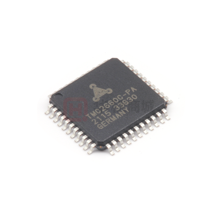


 工商网监
湘ICP备2023018690号
工商网监
湘ICP备2023018690号
