POWER DRIVER FOR STEPPER MOTORS
INTEGRATED CIRCUITS
TMC5161 DATASHEET
Compact, low power-dissipation Driver & Controller for two-phase stepper motors. StealthChop™ for
quiet movement. Up to 5.5A peak coil current. With Step/Dir Interface and SPI.
APPLICATIONS
High-speed 3D Printers
Robotics & Industrial Drives
Packing Machines
Textile, Sewing Machines
Lab & Office Automation
Medical Drives
Liquid Handling
Office Automation
CCTV
ATM, Cash Recycler
CNC Machines
FEATURES
AND
BENEFITS
DESCRIPTION
2-phase stepper motors up to 3.5A RMS coil current
Step/Dir Interface with 3D optimized interpolation MicroPlyer™
Motion Controller with SixPoint™ ramp as intelligent peripheral
Voltage Range 8 … 40V DC (55V peak)
Low RDSon integrated 45mΩ MOSFETs
SPI & Single Wire UART
Encoder Interface and 2x Ref.-Switch Input
Highest Resolution 256 microsteps per full step
StealthChop2™ for quiet operation and smooth motion
Resonance Dampening for mid-range resonances
SpreadCycle™ highly dynamic motor control chopper
DcStep™ load dependent speed control
StallGuard2™ high precision sensorless motor load detection
CoolStep™ current control for energy savings up to 75%
Passive Braking and freewheeling mode
Full Protection & Diagnostics
Compact Size 10x10mm2 aQFN
The TMC5161 is a highly compact stepper
motor controller and driver IC. Its power
stage is optimized for lowest power dissipation and highest dynamics with
Nema 17 and Nema 23 motors. It combines a flexible ramp generator for automatic target positioning with industries’
most advanced stepper motor driver.
Based on TRINAMICs sophisticated
SpreadCycle and StealthChop choppers, it
ensures absolutely noiseless operation
combined with maximum efficiency and
best motor torque. High integration, high
energy efficiency and a small form factor
enable miniaturized and scalable systems
for cost effective solutions. The complete
solution reduces learning curve to a
minimum while giving best performance
in class. Interface-compatible to TMC5160.
BLOCK DIAGRAM
Ref. Switches
Step/Dir
+VM
1 of 2 full bridges
shown
Reference Switch
Processing
Interrupts
TMC5161
CBOOT
Step Multiplyer
CBOOT
Position
Pulse Output
Motor
SPI
UART
UART
Single Wire
MOTION CONTROLLER
with Linear 6 Point
RAMP Generator
SPI to
Master
Programmable
256 µStep
Sequencer
spreadCycle
stealthChop
Protection
& Diagnostics
MOSFET
Power
Stage
Power
Supply
Charge
Pump
CLK
Oscillator / Selector
Encoder Unit
stallGuard2
coolStep
dcStep
Diff. Sensing
CLK
ABN
TRINAMIC Motion Control GmbH & Co. KG
Hamburg, Germany
RSENSE
�TMC5161 DATASHEET (Rev. 1.02 / 2019-FEB-05)
2
APPLICATION EXAMPLES: COMPACT DRIVES – MULTIPURPOSE USE
The TMC5161 scores with complete motion controlling features, a powerful integrated MOSFET driver stage,
and high-quality current regulation. It offers a versatility that covers a wide spectrum of applications from
battery powered, high efficiency systems up to embedded applications with 4A motor current per coil. The
TMC5161 contains the complete intelligence which is required to drive a motor. Receiving target positions
the TMC5161 manages motor movement. Based on TRINAMICs unique features StallGuard2, CoolStep,
DcStep, SpreadCycle, and StealthChop, the TMC5161 optimizes drive performance. It trades off velocity vs.
motor torque, optimizes energy efficiency, smoothness of the drive, and noiselessness. The small form
factor of the TMC5161 keeps costs down and allows for miniaturized layouts. Extensive support at the chip,
board, and software levels enables rapid design cycles and fast time-to-market with competitive products.
High energy efficiency and reliability deliver cost savings in related systems such as power supplies and
cooling. For smaller designs, the compatible, integrated TMC5130 driver provides 1.4A of motor current.
MINIATURIZED DESIGN
FOR ONE
STEPPER MOTOR
Ref.
Switches
High-Level
Interface
SPI
CPU
TMC5161
M
An ABN encoder interface with scaler unit
and two reference switch inputs are used to
ensure correct motor movement. Automatic
interrupt upon deviation is available.
Encoder
COMPACT DESIGN
High-Level
Interface
FOR MULTIPLE
STEPPER MOTORS
SPI or
UART
CPU
TMC5161
M
Addr.
NCS signal for SPI
Chaining
with UART
TMC5161
An application with 2 stepper motors is
shown. Additionally, the ABN Encoder
interface and two reference switches can be
used for each motor. A single CPU controls
the whole system, as there are no real time
tasks required to move a motor. The CPUboard and the controller / driver boards are
highly economical and space saving.
M
Addr.
More TMC5160 or TMC5130 or TMC5072
The TMC5161-EVAL is part of TRINAMICs
universal evaluation board system which
provides a convenient handling of the
hardware as well as a user-friendly
software tool for evaluation. The
TMC5161 evaluation board system
consists
of
three
parts:
LANDUNGSBRÜCKE
(base
board),
ESELSBRÜCKE (connector board including
several test points), and TMC5161-EVAL.
ORDER CODES
Order code
TMC5161-AA
TMC5161-AA-T
TMC5161-EVAL
LANDUNGSBRÜCKE
ESELSBRÜCKE
www.trinamic.com
Description
stepper controller/driver with internal MOSFETs; QFN10x10
-T denotes tape on reel packed devices
Evaluation board for TMC5161 two phase stepper motor
controller/driver
Baseboard for TMC5161-EVAL and further evaluation boards.
Connector board for plug-in evaluation board system.
Size [mm2]
10 x 10
85 x 55
85 x 55
61 x 38
�TMC5161 DATASHEET (Rev. 1.02 / 2019-FEB-05)
3
Table of Contents
1
1.1
1.2
1.3
1.4
1.5
1.6
1.7
KEY CONCEPTS ................................................ 6
CONTROL INTERFACES ..................................... 7
SOFTWARE ...................................................... 7
MOVING AND CONTROLLING THE MOTOR ........ 8
AUTOMATIC STANDSTILL POWER DOWN......... 8
STEALTHCHOP2 & SPREADCYCLE DRIVER ....... 8
STALLGUARD2 – MECHANICAL LOAD SENSING .
....................................................................... 9
1.8
COOLSTEP – LOAD ADAPTIVE CURRENT
CONTROL ...................................................................... 9
1.9
DCSTEP – LOAD DEPENDENT SPEED CONTROL .
.....................................................................10
1.10 ENCODER INTERFACE .....................................10
2
PIN ASSIGNMENTS .........................................11
2.1
2.2
3
SPI DATAGRAM STRUCTURE .........................19
SPI SIGNALS ................................................20
TIMING .........................................................21
UART SINGLE WIRE INTERFACE ................22
5.1
5.2
5.3
5.4
6
STANDARD APPLICATION CIRCUIT ................15
EXTERNAL GATE VOLTAGE REGULATOR ..........16
MOSFETS AND SLOPE CONTROL ..................17
DRIVER PROTECTION AND EME CIRCUITRY ...18
SPI INTERFACE ................................................19
4.1
4.2
4.3
5
PACKAGE OUTLINE ........................................11
SIGNAL DESCRIPTIONS .................................11
SAMPLE CIRCUITS ..........................................15
3.1
3.2
3.3
3.4
4
DATAGRAM STRUCTURE .................................22
CRC CALCULATION .......................................24
UART SIGNALS ............................................24
ADDRESSING MULTIPLE SLAVES ....................25
REGISTER MAPPING .......................................27
6.1
GENERAL CONFIGURATION REGISTERS ..........28
6.2
VELOCITY DEPENDENT DRIVER FEATURE
CONTROL REGISTER SET .............................................34
6.3
RAMP GENERATOR REGISTERS .......................36
6.4
ENCODER REGISTERS .....................................41
6.5
MOTOR DRIVER REGISTERS ...........................43
7
STEALTHCHOP™ ..............................................53
7.1
7.2
7.3
7.4
7.5
7.6
7.7
8
8.1
8.2
PRINCIPLES OF OPERATION ......................... 5
AUTOMATIC TUNING .....................................53
STEALTHCHOP OPTIONS ................................56
STEALTHCHOP CURRENT REGULATOR.............56
VELOCITY BASED SCALING ............................58
COMBINING STEALTHCHOP AND SPREADCYCLE .
.....................................................................60
FLAGS IN STEALTHCHOP ...............................62
FREEWHEELING AND PASSIVE BRAKING ........62
SPREADCYCLE AND CLASSIC CHOPPER ...64
www.trinamic.com
9
SPREADCYCLE CHOPPER................................ 65
CLASSIC CONSTANT OFF TIME CHOPPER ...... 68
SELECTING SENSE RESISTORS.................... 70
10
VELOCITY BASED MODE CONTROL ....... 72
11
DIAGNOSTICS AND PROTECTION......... 74
11.1
11.2
11.3
12
12.1
12.2
12.3
12.4
13
13.1
13.2
13.3
13.4
13.5
14
14.1
14.2
14.3
15
15.1
15.2
15.3
16
16.1
16.2
17
TEMPERATURE SENSORS ................................ 74
SHORT PROTECTION ...................................... 74
OPEN LOAD DIAGNOSTICS ........................... 76
RAMP GENERATOR ..................................... 77
REAL WORLD UNIT CONVERSION ................. 77
MOTION PROFILES........................................ 78
VELOCITY THRESHOLDS ................................. 80
REFERENCE SWITCHES .................................. 81
STALLGUARD2 LOAD MEASUREMENT ... 83
TUNING STALLGUARD2 THRESHOLD SGT ..... 84
STALLGUARD2 UPDATE RATE AND FILTER .... 86
DETECTING A MOTOR STALL ......................... 86
HOMING WITH STALLGUARD......................... 86
LIMITS OF STALLGUARD2 OPERATION .......... 86
COOLSTEP OPERATION ............................. 87
USER BENEFITS............................................. 87
SETTING UP FOR COOLSTEP .......................... 87
TUNING COOLSTEP ....................................... 89
STEP/DIR INTERFACE ................................ 90
TIMING ......................................................... 90
CHANGING RESOLUTION ............................... 91
MICROPLYER AND STAND STILL DETECTION . 92
DIAG OUTPUTS ........................................... 93
STEP/DIR MODE ......................................... 93
MOTION CONTROLLER MODE ........................ 93
DCSTEP .......................................................... 95
17.1 USER BENEFITS............................................. 95
17.2 DESIGNING-IN DCSTEP ................................ 95
17.3 DCSTEP INTEGRATION WITH THE MOTION
CONTROLLER .............................................................. 96
17.4 STALL DETECTION IN DCSTEP MODE ............ 96
17.5 MEASURING ACTUAL MOTOR VELOCITY IN
DCSTEP OPERATION .................................................. 97
17.6 DCSTEP WITH STEP/DIR INTERFACE ........... 98
18
18.1
18.2
19
SINE-WAVE LOOK-UP TABLE................. 101
USER BENEFITS........................................... 101
MICROSTEP TABLE ...................................... 101
EMERGENCY STOP .................................... 102
20
ABN INCREMENTAL ENCODER
INTERFACE ............................................................... 103
�TMC5161 DATASHEET (Rev. 1.02 / 2019-FEB-05)
20.1 ENCODER TIMING ....................................... 104
20.2 SETTING THE ENCODER TO MATCH MOTOR
RESOLUTION ............................................................ 104
20.3 CLOSING THE LOOP .................................... 105
21
21.1
DC MOTOR OR SOLENOID .................... 106
SOLENOID OPERATION ............................... 106
22
QUICK CONFIGURATION GUIDE ......... 107
23
GETTING STARTED .................................. 112
23.1
INITIALIZATION EXAMPLES ......................... 112
24
STANDALONE OPERATION .................... 113
25
EXTERNAL RESET ...................................... 115
26
CLOCK OSCILLATOR AND INPUT ........ 115
26.1
26.2
USING THE INTERNAL CLOCK...................... 115
USING AN EXTERNAL CLOCK....................... 115
27
ABSOLUTE MAXIMUM RATINGS.......... 116
28
ELECTRICAL CHARACTERISTICS .......... 116
28.1
28.2
OPERATIONAL RANGE ................................ 116
DC AND TIMING CHARACTERISTICS ........... 117
www.trinamic.com
4
28.3
29
29.1
29.2
29.3
29.4
29.5
30
30.1
30.2
THERMAL CHARACTERISTICS........................ 119
LAYOUT CONSIDERATIONS................... 122
EXPOSED DIE PADS .................................... 122
POWER SUPPLY PINS ................................. 122
WIRING GND ............................................ 122
SUPPLY FILTERING...................................... 122
LAYOUT EXAMPLE ....................................... 123
PACKAGE MECHANICAL DATA.............. 125
DIMENSIONAL DRAWINGS AQFN ............... 125
PACKAGE CODES ......................................... 126
31
DESIGN PHILOSOPHY ............................. 127
32
DISCLAIMER ............................................... 127
33
ESD SENSITIVE DEVICE.......................... 127
34
TABLE OF FIGURES .................................. 128
35
REVISION HISTORY ................................. 129
36
REFERENCES ............................................... 129
�TMC5161 DATASHEET (Rev. 1.02 / 2019-FEB-05)
1
5
Principles of Operation
The TMC5161 motion controller and driver chip is an intelligent power component interfacing between
CPU and a high power stepper motor. All stepper motor logic is completely within the TMC5161. No
software is required to control the motor – just provide target positions. The TMC5161 offers a
number of unique enhancements which are enabled by the system-on-chip integration of driver and
controller. The sixPoint ramp generator of the TMC5161 uses StealthChop, DcStep, CoolStep, and
StallGuard2 automatically to optimize every motor movement. The TMC5161 ideally extends the
TMC220x, TMC222x, TMC2100, TMC2130 and TMC5130 family to higher motor currents.
THE TMC5161 OFFERS THREE BASIC MODES OF OPERATION:
MODE 1: Full Featured Motion Controller & Driver
All stepper motor logic is completely within the TMC5161. No software is required to control the
motor – just provide target positions. Enable this mode by tying low pin SD_MODE.
MODE 2: Step & Direction Driver
An external high-performance S-ramp motion controller like the TMC4361 or a central CPU generates
step & direction signals synchronized to other components like additional motors within the system.
The TMC5161 takes care of intelligent current and mode control and delivers feedback on the state of
the motor. The MicroPlyer automatically smoothens motion. Tie SD_MODE high.
MODE 3: Simple Step & Direction Driver
The TMC5161 positions the motor based on step & direction signals. The MicroPlyer automatically
smoothens motion. No CPU interaction is required; configuration is done by hardware pins. Basic
standby current control can be done by the TMC5161. Optional feedback signals allow error detection
and synchronization. Enable this mode by tying pin SPI_MODE low and SD_MODE high.
100n
16V
VSA
12VOUT
100n
2.2µ
2.2µ
5VOUT
CE
VM
470n
VS
VCP
CPI
22n
100V
CPO
+VM
REFR/DIR
REFL/STEP
+VM
CB2
11.5V Voltage
regulator
TMC5161
Ref. switch
processing
charge pump
CB
HS
CB1
5V Voltage
regulator
CB
HS
2R2
VCC
linear 6 point
RAMP generator
470n
OB1
Step &
Direction pulse
generation
OB2
LS
CSN
SCK
SDI
SDO
DIAG1/SWP
DIAG0/SWN
RSB
LS
SPI interface
Control register
set
DIAG / INT out
and
Single wire
interface
programmable
sine table
4*256 entry
x
47R
RS
SRBL
Stepper driver
CA2
B.Dwersteg, ©
Protection
TRINAMIC 2014
B.Dwersteg, ©
TRINAMIC 2014
& diagnostics
CB
HS
CA1
CLK_IN
S
47R
CB
HS
coolStep
opt. ext. clock
12-16MHz
SRBH
spreadCycle &
stealthChop
Chopper
OA1
stallGuard2
OA2
dcStep
+VIO
3.3V or 5V
I/O voltage
LS
VCC_IO
RSA
100n
LS
Encoder
unit
mode selection
A
B
SRAH
47R
N
RS
SRAL
pd
Encoder input /
+VIO
+VIO
dcStep control in S/D
mode
Both GND: UART mode
GNDD
GNDA
DIE PAD
TST_MODE
DRV_ENN
47R
ENCN_DCO
ENCA_DCIN
pd
ENCB_DCEN
SPI_MODE
SD_MODE
pd
opt. driver enable
Figure 1.1 TMC5161 basic application block diagram (motion controller)
www.trinamic.com
N
stepper
motor
�TMC5161 DATASHEET (Rev. 1.02 / 2019-FEB-05)
6
100n
16V
VS
CPI
VSA
CB2
12VOUT
100n
2.2µ
TMC5161
11.5V Voltage
regulator
5VOUT
2.2µ
CE
VM
470n
VCP
22n
100V
CPO
+VM
DIR
STEP
+VM
charge pump
CB
HS
step multiplier
microPlyer
5V Voltage
regulator
CB
CB1
HS
Standstill
current
reduction
2R2
VCC
OB1
OB2
470n
LS
RSB
CSN
SCK
SDI
SDO
LS
SPI interface
Control register
set
DIAG / INT out
and
Single wire
interface
DIAG1
DIAG0
programmable
sine table
4*256 entry
x
47R
RS
SRBL
S
Stepper driver
B.Dwersteg, ©
Protection
TRINAMIC 2014
& diagnostics
B.Dwersteg, ©
TRINAMIC 2014
stepper
motor
N
stepper
motor
CA2
CB
HS
CB
CA1
CLK_IN
N
47R
HS
coolStep
opt. ext. clock
12-16MHz
SRBH
spreadCycle &
stealthChop
Chopper
OA1
stallGuard2
OA2
dcStep
+VIO
3.3V or 5V
I/O voltage
LS
VCC_IO
RSA
LS
100n
SRAH
47R
mode selection
RS
SRAL
GNDD
GNDA
DIE PAD
TST_MODE
DCEN
47R
DRV_ENN
+VIO
pd
DCO
SPI_MODE
+VIO
pd
DCIN
SD_MODE
pd
dcStep control
opt. driver enable
Figure 1.2 TMC5161 STEP/DIR application diagram
100n
16V
VSA
100n
2.2µ
2.2µ
CE
VM
470n
VS
VCP
CPI
CPO
+VM
DIR
STEP
+VM
22n
100V
CB2
12VOUT
11.5V Voltage
regulator
5VOUT
5V Voltage
regulator
TMC5161
charge pump
CB
HS
step multiplier
microPlyer
CB1
CB
HS
Standstill
current
reduction
2R2
VCC
OB1
OB2
470n
LS
CFG0
Microstep Resolution
8 / 16 / 32 / 64
RSB
CFG1
LS
CFG2
Run Current Setting
16 / 18 / 20 / 22 /
24 / 26 / 28 / 31
CFG3
CFG4
spreadCycle (GND) /
stealthChop (VCC_IO)
Current Reduction
Enable (VCC_IO)
CFG5
pd
Configuration
interface
(GND or VCC_IO
level)
pd
B.Dwersteg, ©
TRINAMIC 2014
CFG6
Control register
set (default
values)
programmable
sine table
4*256 entry
x
47R
RS
SRBL
CA2
Index pulse
CA1
CB
HS
DIAG0
Driver error
CB
HS
DIAG1
opt. ext. clock
12-16MHz
S
47R
Stepper driver
B.Dwersteg, ©
Protection
TRINAMIC 2014
& diagnostics
B.Dwersteg, ©
TRINAMIC 2014
SRBH
spreadCycle &
stealthChop
Chopper
Status out
(open drain)
OA1
OTP
CLK_IN
OA2
LS
+VIO
3.3V or 5V
I/O voltage
RSA
VCC_IO
100n
LS
SRAH
47R
mode selection
RS
SRAL
+VIO
Standalone mode
GNDA
GNDD
DIE PAD
DRV_ENN
TST_MODE
47R
SPI_MODE
SD_MODE
pd
dcStep control
opt. driver enable
Figure 1.3 TMC5161 standalone driver application diagram
1.1 Key Concepts
The TMC5161 implements advanced features which are exclusive to TRINAMIC products. These features
contribute toward greater precision, greater energy efficiency, higher reliability, smoother motion, and
cooler operation in many stepper motor applications.
www.trinamic.com
�TMC5161 DATASHEET (Rev. 1.02 / 2019-FEB-05)
7
StealthChop2™ No-noise, high-precision chopper algorithm for inaudible motion and inaudible
standstill of the motor. Allows faster motor acceleration and deceleration than
StealthChop™ and extends StealthChop to low stand still motor currents.
SpreadCycle™
High-precision chopper algorithm for highly dynamic motion and absolutely clean
current wave. Low noise, low resonance and low vibration chopper.
DcStep™
Load dependent speed control. The motor moves as fast as possible and never loses
a step.
StallGuard2™
Sensorless stall detection and mechanical load measurement.
CoolStep™
Load-adaptive current control reducing energy consumption by as much as 75%.
MicroPlyer™
Microstep interpolator for obtaining full 256 microstep smoothness with lower
resolution step inputs starting from fullstep
In addition to these performance enhancements, TRINAMIC motor drivers offer safeguards to detect
and protect against shorted outputs, output open-circuit, overtemperature, and undervoltage
conditions for enhancing safety and recovery from equipment malfunctions.
1.2 Control Interfaces
The TMC5161 supports both, an SPI interface and a UART based single wire interface with CRC
checking. Selection of the actual interface is done via the configuration pin SW_SEL, which can be
hardwired to GND or VCC_IO depending on the desired interface.
1.2.1
SPI Interface
The SPI interface is a bit-serial interface synchronous to a bus clock. For every bit sent from the bus
master to the bus slave another bit is sent simultaneously from the slave to the master.
Communication between an SPI master and the TMC5161 slave always consists of sending one 40-bit
command word and receiving one 40-bit status word.
The SPI command rate typically is a few commands per complete motor motion.
1.2.2
UART Interface
The single wire interface allows differential operation similar to RS485 (using SWP and SWN) or single
wire interfacing (leaving open SWN). It can be driven by any standard UART. No baud rate
configuration is required.
1.3 Software
From a software point of view the TMC5161 is a peripheral with a number of control and status
registers. Most of them can either be written only or read only. Some of the registers allow both read
and write access. In case read-modify-write access is desired for a write only register, a shadow
register can be realized in master software.
www.trinamic.com
�TMC5161 DATASHEET (Rev. 1.02 / 2019-FEB-05)
8
1.4 Moving and Controlling the Motor
1.4.1
Integrated Motion Controller
The integrated 32 bit motion controller automatically drives the motor to target positions, or
accelerates to target velocities. All motion parameters can be changed on the fly. The motion
controller recalculates immediately. A minimum set of configuration data consists of acceleration and
deceleration values and the maximum motion velocity. A start and stop velocity is supported as well
as a second acceleration and deceleration setting. The integrated motion controller supports
immediate reaction to mechanical reference switches and to the sensorless stall detection StallGuard2.
Benefits are:
Flexible ramp programming
Efficient use of motor torque for acceleration and deceleration allows higher machine throughput
Immediate reaction to stop and stall conditions
1.4.2
STEP/DIR Interface
The motor can optionally be controlled by a step and direction input. In this case, the motion
controller remains unused. Active edges on the STEP input can be rising edges or both rising and
falling edges as controlled by another mode bit (dedge). Using both edges cuts the toggle rate of the
STEP signal in half, which is useful for communication over slow interfaces such as optically isolated
interfaces. On each active edge, the state sampled from the DIR input determines whether to step
forward or back. Each step can be a fullstep or a microstep, in which there are 2, 4, 8, 16, 32, 64, 128,
or 256 microsteps per fullstep. A step impulse with a low state on DIR increases the microstep
counter and a high decreases the counter by an amount controlled by the microstep resolution. An
internal table translates the counter value into the sine and cosine values which control the motor
current for microstepping.
1.5 Automatic Standstill Power Down
An automatic current reduction drastically reduces application power dissipation and cooling
requirements. Modify stand still current, delay time and decay via register settings. Automatic
freewheeling and passive motor braking are provided as an option for stand still. Passive braking
reduces motor standstill power consumption to zero, while still providing effective dampening and
braking! An option for faster detection of standstill is provided for both, ramp generator and STEP/DIR
operation.
STEP
Standstill flag
(stst)
CURRENT
IRUN
IHOLD
RMS motor current trace
standstill delay TPOWERDOWN IHOLDDELAY
2^20 / 2^18 clocks power down power down
ramp time
(faststandstill)
delay time
t
Figure 1.4 Automatic Motor Current Power Down
1.6 StealthChop2 & SpreadCycle Driver
StealthChop is a voltage chopper based principle. It especially guarantees that the motor is absolutely
quiet in standstill and in slow motion, except for noise generated by ball bearings. Unlike other
voltage mode choppers, StealthChop2 does not require any configuration. It automatically learns the
best settings during the first motion after power up and further optimizes the settings in subsequent
motions. An initial homing sequence is sufficient for learning. Optionally, initial learning parameters
www.trinamic.com
�TMC5161 DATASHEET (Rev. 1.02 / 2019-FEB-05)
9
can be pre-configured via the interface. StealthChop2 allows high motor dynamics, by reacting at once
to a change of motor velocity.
For highest dynamic applications, SpreadCycle is an option to StealthChop2. It can be enabled via
input pin (standalone mode) or via SPI or UART interface. StealthChop2 and SpreadCycle may even be
used in a combined configuration for the best of both worlds: StealthChop2 for no-noise stand still,
silent and smooth performance, SpreadCycle at higher velocity for high dynamics and highest peak
velocity at low vibration.
SpreadCycle is an advanced cycle-by-cycle chopper mode. It offers smooth operation and good
resonance dampening over a wide range of speed and load. The SpreadCycle chopper scheme
automatically integrates and tunes fast decay cycles to guarantee smooth zero crossing performance.
Benefits of using StealthChop2:
- Significantly improved microstepping with low cost motors
- Motor runs smooth and quiet
- Absolutely no standby noise
- Reduced mechanical resonance yields improved torque
1.7 StallGuard2 – Mechanical Load Sensing
StallGuard2 provides an accurate measurement of the load on the motor. It can be used for stall
detection as well as other uses at loads below those which stall the motor, such as CoolStep loadadaptive current reduction. This gives more information on the drive allowing functions like
sensorless homing and diagnostics of the drive mechanics.
1.8 CoolStep – Load Adaptive Current Control
CoolStep drives the motor at the optimum current. It uses the StallGuard2 load measurement
information to adjust the motor current to the minimum amount required in the actual load situation.
This saves energy and keeps the components cool.
Benefits are:
- Energy efficiency
- Motor generates less heat
- Less or no cooling
- Use of smaller motor
power consumption decreased up to 75%
improved mechanical precision
improved reliability
less torque reserve required → cheaper motor does the job
Figure 1.5 shows the efficiency gain of a 42mm stepper motor when using CoolStep compared to
standard operation with 50% of torque reserve. CoolStep is enabled above 60RPM in the example.
0,9
Efficiency with coolStep
0,8
Efficiency with 50% torque reserve
0,7
0,6
0,5
Efficiency
0,4
0,3
0,2
0,1
0
0
50
100
150
200
250
300
350
Velocity [RPM]
Figure 1.5 Energy efficiency with CoolStep (example)
www.trinamic.com
�TMC5161 DATASHEET (Rev. 1.02 / 2019-FEB-05)
10
1.9 DcStep – Load Dependent Speed Control
DcStep allows the motor to run near its load limit and at its velocity limit without losing a step. If
the mechanical load on the motor increases to the stalling load, the motor automatically decreases
velocity so that it can still drive the load. With this feature, the motor will never stall. In addition to
the increased torque at a lower velocity, dynamic inertia will allow the motor to overcome mechanical
overloads by decelerating. DcStep directly integrates with the ramp generator, so that the target
position will be reached, even if the motor velocity needs to be decreased due to increased
mechanical load. A dynamic range of up to factor 10 or more can be covered by DcStep without any
step loss. By optimizing the motion velocity in high load situations, this feature further enhances
overall system efficiency.
Benefits are:
- Motor does not loose steps in overload conditions
- Application works as fast as possible
- Highest possible acceleration automatically
- Highest energy efficiency at speed limit
- Highest possible motor torque using fullstep drive
- Cheaper motor does the job
1.10 Encoder Interface
The TMC5161 provides an encoder interface for external incremental encoders. The encoder provides
automatic checking for step loss and can be used for homing of the motion controller (alternatively to
reference switches). A programmable prescaler allows the adaptation of the encoder resolution to the
motor resolution. A 32 bit encoder counter is provided.
www.trinamic.com
�TMC5161 DATASHEET (Rev. 1.02 / 2019-FEB-05)
2
11
Pin Assignments
2.1 Package Outline
NC3
NC2
16
17
18
19
20
21
22
23
24
25
26
27
SDI_CFG1
SDO_CFG0
REFL_STEP
REFR_DIR
VCC_IO
SD_MODE
SPI_MODE
ENCB_DCEN_CFG4
ENCA_DCIN_CFG5
GNDD
ENCN_DCO_CFG6
15
CSN_CFG3
SCK_CFG2
14
CLK
x
38
37
36
35
34
33
32
31
30
29
28
GNDP
13
x
TST_MODE
x
12
x
OA2
1
2
3
4
5
6
7
8
9
10
11
SRBL
CB1
12VOUT
VSA
5VOUT
GNDA
SRAL
SRAH
SRBH
NC1
VM
x
CA1
CB2
OB1
RSA
OA1
OB2
NC4
RSB
x
CA2
VCP
VS
CPI
CPO
VCC
DRV_ENN
DIAG1_SWP
DIAG0_SWN
x
x
x
Figure 2.1 TMC5161-LA package and pinning QFN (10x10mm²)
2.2 Signal Descriptions
Pin
CB1
Pin
1
12VOUT
2
unused / x
3, 5, 9,
30, 36, x
www.trinamic.com
Type
Function
Bootstrap capacitor positive connection.
Output of internal 11.5V gate voltage regulator and supply pin
of low side gate drivers. Attach 2.2µF (to 10µF) ceramic
capacitor to GND plane near to pin for best performance. In
case an external gate voltage supply is available, tie VSA and
12VOUT to the external supply.
Unused pins. May be left open or connected to any potential.
The corner pins should be soldered to improve centering.
�TMC5161 DATASHEET (Rev. 1.02 / 2019-FEB-05)
Pin
Pin
VSA
4
5VOUT
6
GNDA
7
SRAL
8
AI
SRAH
10
AI
SRBH
11
AI
SRBL
12
AI
TST_MODE
13
DI
CLK
14
DI
CSN_CFG3
15
DI
SCK_CFG2
16
DI
SDI_CFG1
17
DI
SDO_CFG0
18
DIO
REFL_STEP
19
DI
REFR_DIR
20
DI
VCC_IO
21
SD_MODE
22
DI
SPI_MODE
23
DI
(pd)
ENCB_DCEN_
CFG4
24
DI
(pd)
www.trinamic.com
Type
Function
Analog supply voltage for 11.5V and 5V regulator. Normally
tied to VS. Provide a 100nF filtering capacitor.
Output of internal 5V regulator. Attach 2.2µF to 10µF ceramic
capacitor to GNDA near to pin for best performance. Output
for VCC supply of the chip.
Analog GND. Connect to GND plane near pin.
Sense resistor GND connection for phase A. Connect to the
GND side of the sense resistor in order to compensate for
voltage drop on the GND interconnection.
Sense resistor for phase A. Connect to the upper side of the
sense resistor. A Kelvin connection is preferred with high
motor currents. Symmetrical RC-Filtering may be added for
SRAL and SRAH to eliminate high frequency switching spikes
from other drives or switching of coil B.
Sense resistor for phase B. Connect to the upper side of the
sense resistor. A Kelvin connection is preferred with high
motor currents. Symmetrical RC-Filtering may be added for
SRBL and SRBH to eliminate high frequency switching spikes
from other drives or switching of coil A.
Sense resistor GND connection for phase B. Connect to the
GND side of the sense resistor in order to compensate for
voltage drop on the GND interconnection.
Test mode input. Tie to GND using short wire.
CLK input. Tie to GND using short wire for internal clock or
supply external clock. Internal clock-fail over circuit protects
against loss of external clock signal.
SPI chip select input (negative active) (SPI_MODE=1) or
Configuration input (SPI_MODE=0)
SPI serial clock input (SPI_MODE=1) or
Configuration input (SPI_MODE=0)
SPI data input (SPI_MODE=1) or
Configuration input (SPI_MODE=0) or
Next address input (NAI) for single wire interface.
SPI data output (tristate) (SPI_MODE=1) or
Configuration input (SPI_MODE=0) or
Next address output (NAO) for single wire interface.
Left reference input (for internal ramp generator) or
STEP input when (SD_MODE=1).
Right reference input (for internal ramp generator) or
DIR input (SD_MODE=1).
3.3V to 5V IO supply voltage for all digital pins.
Mode selection input. When tied low, the internal ramp
generator generates step pulses. When tied high, the STEP/DIR
inputs control the driver. SD_MODE=0 and SPI_MODE=0 enable
UART operation.
Mode selection input. When tied low with SD_MODE=1, the
chip is in standalone mode and pins have their CFG functions.
When tied high, the SPI interface is enabled. Integrated pull
down resistor.
Encoder B-channel input (when using internal ramp generator)
or
DcStep enable input (SD_MODE=1, SPI_MODE=1) – leave open
or tie to GND for normal operation in this mode (no DcStep).
Configuration input (SPI_MODE=0)
12
�TMC5161 DATASHEET (Rev. 1.02 / 2019-FEB-05)
Pin
Pin
Type
ENCA_DCIN_
CFG5
25
DI
(pd)
GNDD
26
ENCN_DCO_
CFG6
27
DIO
DIAG0_SWN
28
DIO
(pu+
pd)
DIAG1_SWP
29
DIO
(pd)
DRV_ENN
31
DI
VCC
32
CPO
33
CPI
34
VS
35
VCP
37
VM
VM
OA2
RSA
OA1
CA1
CB2
OB2
RSB
OB1
OA2
RSA
OA1
CA1
CB2
OB2
RSB
OB1
NC1-NC4
NC1-NC4
www.trinamic.com
Function
Encoder A-channel input (when using internal ramp generator)
or
DcStep gating input for axis synchronization (SD_MODE=1,
SPI_MODE=1) or
Configuration input (SPI_MODE=0)
Digital GND. Connect to GND plane near pin.
Encoder N-channel input (SD_MODE=0) or
DcStep ready output (SD_MODE=1).
With SD_MODE=0, pull to GND or VCC_IO, if the pin is not
used.
Diagnostics output DIAG0.
Interrupt or STEP output for motion controller (SD_MODE=0,
SPI_MODE=1).
Use external pullup resistor with 47k or less in open drain
mode.
Single wire I/O (negative) (only with SD_MODE=0 and
SPI_MODE=0)
Diagnostics output DIAG1.
Position compare or DIR output for motion controller
(SD_MODE=0, SPI_MODE=1).
Use external pullup resistor with 47k or less in open drain
mode.
Single wire I/O (positive) (only with SD_MODE=0 and
SPI_MODE=0)
Enable input. The power stage becomes switched off (all
motor outputs floating) when this pin is driven high.
5V supply input for digital circuitry within chip. Provide 100nF
or bigger capacitor to GND (GND plane) near pin. Shall be
supplied by 5VOUT. A 2.2 or 3.3 Ohm resistor is recommended
for decoupling noise from 5VOUT. When using an external
supply, make sure, that VCC comes up before or in parallel to
5VOUT or VCC_IO, whichever comes up later!
Charge pump capacitor output.
Charge pump capacitor input. Tie to CPO using 22nF 100V
capacitor.
Motor supply voltage. Provide filtering capacity near pin with
short loop to GND plane. Must be tied to the positive bridge
supply voltage.
Charge pump voltage. Tie to VS using 100nF capacitor.
Motor supply voltage and common cooling terminal for all HS
MOSFETs. Connect to identical potential as VS. Provide filtering
capacity of 470nF or more with direct interconnection to GND
plane, optimally directly left and right of the device.
Motor driver output and cooling terminal for LS MOSFET.
Sense resistor connection.
Motor driver output and cooling terminal for LS MOSFET.
Bootstrap capacitor positive connection.
Bootstrap capacitor positive connection.
Motor driver output and cooling terminal for LS MOSFET.
Sense resistor connection.
Motor driver output and cooling terminal for LS MOSFET.
Do not connect. Internal low side gate. May be left out in PCB
footprint.
13
�TMC5161 DATASHEET (Rev. 1.02 / 2019-FEB-05)
Pin
Pin
GNDPAD
GNDPAD
Type
14
Function
Connect the exposed die pad to a GND plane. Provide as many
as possible vias for heat transfer to GND plane. Serves as GND
pin for the low side gate drivers. Ensure low loop inductivity
to sense resistor GND.
*(pd) denominates a pin with pulldown resistor
* All digital pins DI, DIO and DO use VCC_IO level and contain protection diodes to GND and VCC_IO
* All digital inputs DI and DIO have internal Schmitt-Triggers
www.trinamic.com
�TMC5161 DATASHEET (Rev. 1.02 / 2019-FEB-05)
3
15
Sample Circuits
The following sample circuits show the required external components in different operation and
supply modes. The connection of the bus interface and further digital signals are left out for clarity.
3.1 Standard Application Circuit
100n
16V
VSA
2.2µ
2.2µ
CE
CB2
12VOUT
100n
470n
VM
100n
VS
VCP
CPI
22n
100V
CPO
+VM
REFR/DIR
REFL/STEP
+VM
Optional use lower
voltage down to 12V
11.5V Voltage
regulator
5VOUT
charge pump
reference switch
processing
CB
HS
CB1
5V Voltage
regulator
CB
HS
2R2
OB1
VCC
470n
OB2
TMC5161
LS
RSB
CSN
SCK
SDI
SDO
LS
SRBH
SPI interface
47R
RS
Controller
DIAG / INT out
and
Single wire
interface
DIAG1/SWP
DIAG0/SWN
SRBL
Chopper
S
47R
N
stepper
motor
CA2
B.Dwersteg, ©
TRINAMIC 2014
CB
HS
CA1
CB
HS
opt. ext. clock
12-16MHz
OA1
CLK_IN
OA2
+VIO
3.3V or 5V
I/O voltage
LS
VCC_IO
Keep inductivity of the fat
interconnections as small
as possible to avoid
undershoot of BM 12MHz. A good thermal coupling of the heat slug to the system PCB GND plane is required
to dissipate heat. Still, the thermal thresholds will be lowered significantly by self-heating. To reduce
power dissipation, supply an external gate driver voltage to the TMC5161. Figure 3.2 shows the
required connection. The internal gate voltage regulator becomes disabled in this constellation. 12V
+/-1V are recommended for best results.
12V Gate Voltage
+VG
VSA
12VOUT
2.2µ
5VOUT
2.2µ
11.5V Voltage
regulator
5V Voltage
regulator
2R2
VCC
470n
Figure 3.2 External gate voltage supply
www.trinamic.com
�TMC5161 DATASHEET (Rev. 1.02 / 2019-FEB-05)
17
3.3 MOSFETs and Slope Control
The TMC5161 integrates a discrete MOSFET power stage in order to yield a complete driver. The
MOSFET driver stage allows adaptation of parameters like gate driver current and blank time, in order
to optimally fit the driver with the MOSFETs for the given application. The tiny internal driver stage
operates at 10ns slope with minimum gate driver current setting, which is absolutely sufficient for
minimum power dissipation. Due to the fast slopes, minimum BBM time setting is sufficient.
V12VOUT
Miller plateau
Lx
MOSFET drivers
0V
VVM
Output
slope
BMx
0V
Output
slope
-1.2V
VVM+V12VOUT
VVM
Hx
0V
VCX-VBMx
HxBMx
Miller plateau
0V
tBBM
tBBM
tBBM
Effective break-before-make time
Load pulling BMx down
Load pulling BMx up
Figure 3.3 Slopes, Miller plateau and blank time
The following DRV_CONF parameters allow adapting the driver to the MOSFET bridge:
Parameter
BBMTIME
Description
Break-before-make time setting to ensure nonoverlapping switching of high-side and low-side
MOSFETs. BBMTIME allows fine tuning of times in
increments shorter than a clock period.
As the TMC5161 switches very fast, a setting of 0
is sufficient.
BBMCLKS
Like BBMTIME, but in multiple of a clock cycle.
The longer setting rules (BBMTIME vs. BBMCLKS).
0 to 2 recommended.
As the TMC5161 switches very fast, a setting of 0
is sufficient. However, there is only negligible
difference with settings 2 or 4.
DRV_
Selection of gate driver current. Higher settings
STRENGTH
give faster slopes. 0 recommended.
FILT_ISENSE Filter time constant of sense amplifier to suppress
ringing and coupling from second coil operation
Hint: Increase setting if motor chopper noise
occurs due to cross-coupling of both coils.
(Reset Default = %00)
www.trinamic.com
Setting
0…8
Comment
time[ns]
100ns*32/(32-BBMTIME)
Ensure ~30% headroom
Reset Default: 0
0…15
0: off, use BBMTIME
Reset Default: OTP 4 or 2
0…2
Reset Default = 2
0 recommended.
00: ~100ns (reset default)
01: ~200ns
10: ~300ns
11: ~400ns
0…3
�TMC5161 DATASHEET (Rev. 1.02 / 2019-FEB-05)
18
3.4 Driver Protection and EME Circuitry
Electromagnetic emission is an important optimization area, to keep cost for shielding low. Further,
some applications have to cope with ESD events caused by motor operation or external influence.
Despite ESD circuitry within the driver chips, ESD events occurring during operation can cause a reset
or even a destruction of the motor driver, depending on their energy. Especially plastic housings and
belt drive systems tend to cause ESD events of several kV. It is best practice to avoid ESD events by
attaching all conductive parts, especially the motors themselves to PCB ground, or to apply electrically
conductive plastic parts. In addition, the driver can be protected up to a certain degree against ESD
events or live plugging / pulling the motor, which also causes high voltages and high currents into
the motor connector terminals. A simple scheme uses capacitors at the driver outputs to reduce the
dV/dt caused by MOSFET diode recovery, and additionally caused by external ESD events. Larger
capacitors will bring more benefit concerning ESD suppression, but cause additional current flow in
each chopper cycle, and thus increase driver power dissipation, especially at high supply voltages. The
values shown are example values – they might be varied between 100pF and 1nF. The capacitors
dampen high frequency resulting from MOSFET switching and noise injected from digital parts of the
application PCB circuitry and thus reduce electromagnetic emission. A more elaborate scheme uses LC
filters to de-couple the driver outputs from the motor connector. Varistors in between of the coil
terminals eliminate coil overvoltage caused by live plugging. Optionally protect all outputs by a
varistor against ESD voltage.
470pF
100V
OA1
Full Bridge A
OA1
OA2
S
N
stepper
motor
Full Bridge A
50Ohm @
100MHz
V1A
V1
OA2
50Ohm @
100MHz
470pF
100V
BRA
Driver
RSA
470pF
100V
S
N
stepper
motor
V1B
470pF
100V
Driver
100nF
16V
470pF
100V
OB1
Full Bridge B
OB1
Full Bridge B
OB2
50Ohm @
100MHz
V2A
V2
OB2
50Ohm @
100MHz
470pF
100V
BRB
RSB
100nF
16V
470pF
100V
Fit varistors to supply voltage
rating. SMD inductivities
conduct full motor coil
current.
Figure 3.4 Simple ESD enhancement and more elaborate motor output protection
www.trinamic.com
V2B
470pF
100V
Varistors V1 and V2 protect
against inductive motor coil
overvoltage.
V1A, V1B, V2A, V2B:
Optional position for varistors
in case of heavy ESD events.
�TMC5161 DATASHEET (Rev. 1.02 / 2019-FEB-05)
4
19
SPI Interface
4.1 SPI Datagram Structure
The TMC5161 uses 40 bit SPI™ (Serial Peripheral Interface, SPI is Trademark of Motorola) datagrams
for communication with a microcontroller. Microcontrollers which are equipped with hardware SPI are
typically able to communicate using integer multiples of 8 bit. The NCS line of the device must be
handled in a way, that it stays active (low) for the complete duration of the datagram transmission.
Each datagram sent to the device is composed of an address byte followed by four data bytes. This
allows direct 32 bit data word communication with the register set. Each register is accessed via 32
data bits even if it uses less than 32 data bits.
For simplification, each register is specified by a one byte address:
- For a read access the most significant bit of the address byte is 0.
- For a write access the most significant bit of the address byte is 1.
Most registers are write only registers, some can be read additionally, and there are also some read
only registers.
SPI DATAGRAM STRUCTURE
MSB (transmitted first)
40 bit
39 ...
→ 8 bit address
8 bit SPI status
... 0
→ 32 bit data
39 ... 32
→ to TMC5161
RW + 7 bit address
from TMC5161
8 bit SPI status
W
39 / 38 ... 32
38...32
LSB (transmitted last)
31 ... 0
8 bit data
8 bit data
31 ... 24
31...28
27...24
23 ... 16
23...20
19...16
8 bit data
8 bit data
15 ... 8
15...12
7 ... 0
11...8
7...4
3...0
3 3 3 3 3 3 3 3 3 3 2 2 2 2 2 2 2 2 2 2 1 1 1 1 1 1 1 1 1 1
9 8 7 6 5 4 3 2 1 0
9 8 7 6 5 4 3 2 1 0 9 8 7 6 5 4 3 2 1 0 9 8 7 6 5 4 3 2 1 0
4.1.1
Selection of Write / Read (WRITE_notREAD)
The read and write selection is controlled by the MSB of the address byte (bit 39 of the SPI
datagram). This bit is 0 for read access and 1 for write access. So, the bit named W is a
WRITE_notREAD control bit. The active high write bit is the MSB of the address byte. So, 0x80 has to
be added to the address for a write access. The SPI interface always delivers data back to the master,
independent of the W bit. The data transferred back is the data read from the address which was
transmitted with the previous datagram, if the previous access was a read access. If the previous
access was a write access, then the data read back mirrors the previously received write data. So, the
difference between a read and a write access is that the read access does not transfer data to the
addressed register but it transfers the address only and its 32 data bits are dummies, and, further the
following read or write access delivers back the data read from the address transmitted in the
preceding read cycle.
A read access request datagram uses dummy write data. Read data is transferred back to the master
with the subsequent read or write access. Hence, reading multiple registers can be done in a
pipelined fashion.
Whenever data is read from or written to the TMC5161, the MSBs delivered back contain the SPI
status, SPI_STATUS, a number of eight selected status bits.
www.trinamic.com
�TMC5161 DATASHEET (Rev. 1.02 / 2019-FEB-05)
20
Example:
For a read access to the register (XACTUAL) with the address 0x21, the address byte has to
be set to 0x21 in the access preceding the read access. For a write access to the register
(VACTUAL), the address byte has to be set to 0x80 + 0x22 = 0xA2. For read access, the data
bit might have any value (-). So, one can set them to 0.
action
read XACTUAL
read XACTUAL
write VMAX:= 0x00ABCDEF
write VMAX:= 0x00123456
data sent to TMC5161
→ 0x2100000000
→ 0x2100000000
→ 0xA700ABCDEF
→ 0xA700123456
data received from TMC5161
0xSS & unused data
0xSS & XACTUAL
0xSS & XACTUAL
0xSS00ABCDEF
*)S: is a placeholder for the status bits SPI_STATUS
4.1.2
SPI Status Bits Transferred with Each Datagram Read Back
New status information becomes latched at the end of each access and is available with the next SPI
transfer.
SPI_STATUS – status flags transmitted with each SPI access in bits 39 to 32
Bit
Name
Comment
7
status_stop_r
6
5
4
3
2
1
0
status_stop_l
position_reached
velocity_reached
standstill
sg2
driver_error
reset_flag
RAMP_STAT[1] – 1: Signals stop right switch status (motion controller
only)
RAMP_STAT[0] – 1: Signals stop left switch status (motion controller only)
RAMP_STAT[9] – 1: Signals target position reached (motion controller only)
RAMP_STAT[8] – 1: Signals target velocity reached (motion controller only)
DRV_STATUS[31] – 1: Signals motor stand still
DRV_STATUS[24] – 1: Signals stallGuard flag active
GSTAT[1] – 1: Signals driver 1 driver error (clear by reading GSTAT)
GSTAT[0] – 1: Signals, that a reset has occurred (clear by reading GSTAT)
4.1.3
Data Alignment
All data are right aligned. Some registers represent unsigned (positive) values, some represent integer
values (signed) as two’s complement numbers, single bits or groups of bits are represented as single
bits respectively as integer groups.
4.2 SPI Signals
The SPI bus on the TMC5161 has four signals:
- SCK – bus clock input
- SDI – serial data input
- SDO – serial data output
- CSN – chip select input (active low)
The slave is enabled for an SPI transaction by a low on the chip select input CSN. Bit transfer is
synchronous to the bus clock SCK, with the slave latching the data from SDI on the rising edge of SCK
and driving data to SDO following the falling edge. The most significant bit is sent first. A minimum
of 40 SCK clock cycles is required for a bus transaction with the TMC5161.
If more than 40 clocks are driven, the additional bits shifted into SDI are shifted out on SDO after a
40-clock delay through an internal shift register. This can be used for daisy chaining multiple chips.
CSN must be low during the whole bus transaction. When CSN goes high, the contents of the internal
shift register are latched into the internal control register and recognized as a command from the
master to the slave. If more than 40 bits are sent, only the last 40 bits received before the rising edge
of CSN are recognized as the command.
www.trinamic.com
�TMC5161 DATASHEET (Rev. 1.02 / 2019-FEB-05)
21
4.3 Timing
The SPI interface is synchronized to the internal system clock, which limits the SPI bus clock SCK to
half of the system clock frequency. If the system clock is based on the on-chip oscillator, an additional
10% safety margin must be used to ensure reliable data transmission. All SPI inputs as well as the
ENN input are internally filtered to avoid triggering on pulses shorter than 20ns. Figure 4.1 shows the
timing parameters of an SPI bus transaction, and the table below specifies their values.
CSN
tCC
tCL
tCH
tCH
tCC
SCK
tDU
SDI
bit39
tDH
bit38
bit0
tDO
SDO
tZC
bit39
bit38
bit0
Figure 4.1 SPI timing
Hint
Usually this SPI timing is referred to as SPI MODE 3
SPI interface timing
Parameter
SCK valid before or after change
of CSN
AC-Characteristics
clock period: tCLK
Symbol
tCC
fSCK
fSCK
assumes
synchronous CLK
tCSH
SCK low time
tCL
SCK high time
tCH
www.trinamic.com
Min
Typ
Max
10
*) Min time is for
synchronous CLK
with SCK high one
tCH before CSN high
only
*) Min time is for
synchronous CLK
only
*) Min time is for
synchronous CLK
only
assumes minimum
OSC frequency
CSN high time
SCK frequency using internal
clock
SCK frequency using external
16MHz clock
SDI setup time before rising
edge of SCK
SDI hold time after rising edge
of SCK
Data out valid time after falling
SCK clock edge
SDI, SCK and CSN filter delay
time
Conditions
Unit
ns
tCLK*)
>2tCLK+10
ns
tCLK*)
>tCLK+10
ns
tCLK*)
>tCLK+10
ns
4
MHz
8
MHz
tDU
10
ns
tDH
10
ns
tDO
no capacitive load
on SDO
tFILT
rising and falling
edge
12
20
tFILT+5
ns
30
ns
�TMC5161 DATASHEET (Rev. 1.02 / 2019-FEB-05)
5
22
UART Single Wire Interface
The UART single wire interface allows the control of the TMC5161 with any microcontroller UART. It
shares transmit and receive line like an RS485 based interface. Data transmission is secured using a
cyclic redundancy check, so that increased interface distances (e.g. over cables between two PCBs) can
be bridged without the danger of wrong or missed commands even in the event of electro-magnetic
disturbance. The automatic baud rate detection and an advanced addressing scheme make this
interface easy and flexible to use.
5.1 Datagram Structure
5.1.1
Write Access
UART WRITE ACCESS DATAGRAM STRUCTURE
each byte is LSB…MSB, highest byte transmitted first
0 … 63
8 bit slave
RW + 7 bit
sync + reserved
32 bit data
address
register addr.
56…63
63
…
CRC
56
55
…
24…55
data bytes 3, 2, 1, 0
(high to low byte)
24
1
23
…
16…23
register
address
16
4
15
3
…
2
SLAVEADDR
8
0
7
1
6
0
5
1
1
8…15
Reserved (don’t cares
but included in CRC)
0
0…7
CRC
A sync nibble precedes each transmission to and from the TMC5161 and is embedded into the first
transmitted byte, followed by an addressing byte. Each transmission allows a synchronization of the
internal baud rate divider to the master clock. The actual baud rate is adapted and variations of the
internal clock frequency are compensated. Thus, the baud rate can be freely chosen within the valid
range. Each transmitted byte starts with a start bit (logic 0, low level on SWP) and ends with a stop
bit (logic 1, high level on SWP). The bit time is calculated by measuring the time from the beginning
of start bit (1 to 0 transition) to the end of the sync frame (1 to 0 transition from bit 2 to bit 3). All
data is transmitted byte wise. The 32 bit data words are transmitted with the highest byte first.
A minimum baud rate of 9000 baud is permissible, assuming 20 MHz clock (worst case for low baud
rate). Maximum baud rate is fCLK/16 due to the required stability of the baud clock.
The slave address is determined by the register SLAVEADDR. If the external address pin NEXTADDR is
set, the slave address becomes incremented by one.
The communication becomes reset if a pause time of longer than 63 bit times between the start bits
of two successive bytes occurs. This timing is based on the last correctly received datagram. In this
case, the transmission needs to be restarted after a failure recovery time of minimum 12 bit times of
bus idle time. This scheme allows the master to reset communication in case of transmission errors.
Any pulse on an idle data line below 16 clock cycles will be treated as a glitch and leads to a timeout
of 12 bit times, for which the data line must be idle. Other errors like wrong CRC are also treated the
same way. This allows a safe re-synchronization of the transmission after any error conditions.
Remark, that due to this mechanism an abrupt reduction of the baud rate to less than 15 percent of
the previous value is not possible.
Each accepted write datagram becomes acknowledged by the receiver by incrementing an internal
cyclic datagram counter (8 bit). Reading out the datagram counter allows the master to check the
success of an initialization sequence or single write accesses. Read accesses do not modify the
counter.
www.trinamic.com
�TMC5161 DATASHEET (Rev. 1.02 / 2019-FEB-05)
5.1.2
23
Read Access
UART READ ACCESS REQUEST DATAGRAM STRUCTURE
each byte is LSB…MSB, highest byte transmitted first
8…15
16…23
24…31
31
…
CRC
24
23
0
…
16
register address
15
…
SLAVEADDR
8
0
7
1
6
0
5
1
Reserved (don’t cares
but included in CRC)
4
0...7
3
CRC
2
RW + 7 bit register
address
1
8 bit slave address
0
sync + reserved
The read access request datagram structure is identical to the write access datagram structure, but
uses a lower number of user bits. Its function is the addressing of the slave and the transmission of
the desired register address for the read access. The TMC5161 responds with the same baud rate as
the master uses for the read request.
In order to ensure a clean bus transition from the master to the slave, the TMC5161 does not
immediately send the reply to a read access, but it uses a programmable delay time after which the
first reply byte becomes sent following a read request. This delay time can be set in multiples of
eight bit times using SENDDELAY time setting (default=8 bit times) according to the needs of the
master. In a multi-slave system, set SENDDELAY to min. 2 for all slaves. Otherwise a non-addressed
slaves might detect a transmission error upon read access to a different slave.
UART READ ACCESS REPLY DATAGRAM STRUCTURE
each byte is LSB…MSB, highest byte transmitted first
24…55
data bytes 3, 2, 1, 0
(high to low byte)
56…63
…
CRC
56
55
CRC
…
32 bit data
24
0
23
…
15
3
…
2
16…23
register
address
0xFF
8
1
reserved (0)
7
0
6
1
5
0
8…15
4
1
0
0…7
16
sync + reserved
63
0 ...... 63
8 bit slave
RW + 7 bit
address
register addr.
The read response is sent to the master using address code %1111. The transmitter becomes switched
inactive four bit times after the last bit is sent.
Address %11111111 is reserved for read accesses going to the master. A slave cannot use this
address.
www.trinamic.com
�TMC5161 DATASHEET (Rev. 1.02 / 2019-FEB-05)
24
5.2 CRC Calculation
An 8 bit CRC polynomial is used for checking both read and write access. It allows detection of up to
eight single bit errors. The CRC8-ATM polynomial with an initial value of zero is applied LSB to MSB,
including the sync- and addressing byte. The sync nibble is assumed to always be correct. The
TMC5161 responds only to correctly transmitted datagrams containing its own slave address. It
increases its datagram counter for each correctly received write access datagram.
𝐶𝑅𝐶 = 𝑥 8 + 𝑥 2 + 𝑥 1 + 𝑥 0
SERIAL CALCULATION EXAMPLE
CRC = (CRC 24 not recommended, use BBMCLKS instead
Hint: 0 recommended due to fast switching MOSFETs
(Reset Default = 0)
www.trinamic.com
�TMC5161 DATASHEET (Rev. 1.02 / 2019-FEB-05)
32
GENERAL CONFIGURATION REGISTERS (0X00…0X0F)
R/W
Addr
n
Register
Description / bit names
11..8 BBMCLKS:
0..15: Digital BBM time in clock cycles (typ. 83ns).
The longer setting rules (BBMTIME vs. BBMCLKS).
(Reset Default: 2 via OTP)
Hint: 2, or down to 0 recommended due to fast
switching MOSFETs
17..16 OTSELECT:
Selection of over temperature level for bridge disable,
switch on after cool down to 120°C / OTPW level.
00: 150°C (not recommended – MOSFET might overheat)
01: 143°C
10: 136°C Recommended
11: 120°C (not recommended, no hysteresis)
19..18
21..20
7..0
W
R
0x0B
0x0C
8
16
www.trinamic.com
GLOBAL
SCALER
OFFSET_
READ
Hint: Adapt overtemperature threshold as required to
protect the MOSFETs or other components on the PCB.
(Reset Default = %00)
DRVSTRENGTH:
Selection of gate driver current. Adapts the gate driver
current to the gate charge of the external MOSFETs.
00: Normal slope Recommended
01: Normal+TC (medium above OTPW level)
10: Fast slope
(Reset Default = %10)
FILT_ISENSE:
Filter time constant of sense amplifier to suppress
ringing and coupling from second coil operation
00: low – 100ns
01:
– 200ns
10:
– 300ns
11: high– 400ns
Hint: Increase setting if motor chopper noise occurs
due to cross-coupling of both coils.
(Reset Default = %00)
Global scaling of Motor current. This value is multiplied
to the current scaling in order to adapt a drive to a
certain motor type. This value should be chosen before
tuning other settings, because it also influences
chopper hysteresis.
0:
1 … 31:
32 … 255:
15..8
7..0
Full Scale (or write 256)
Not allowed for operation
32/256 … 255/256 of maximum current.
Hint: Values >128 recommended for best results
(Reset Default = 0)
Offset calibration result phase A (signed)
Offset calibration result phase B (signed)
�TMC5161 DATASHEET (Rev. 1.02 / 2019-FEB-05)
6.1.1
33
OTP_READ – OTP configuration memory
The OTP memory holds power up defaults for certain registers. All OTP memory bits are cleared to 0
by default. Programming only can set bits, clearing bits is not possible. Factory tuning of the clock
frequency affects otp0.0 to otp0.4. The state of these bits therefore may differ between individual ICs.
0X07: OTP_READ – OTP MEMORY MAP
Bit
7
Name
otp0.7
Function
otp_TBL
6
otp0.6
otp_BBM
5
otp0.5
otp_S2_LEVEL
4
3
2
1
0
otp0.4
otp0.3
otp0.2
otp0.1
otp0.0
OTP_FCLKTRIM
www.trinamic.com
Comment
Reset default for TBL:
0: TBL=%10 (~3µs)
1: TBL=%01 (~2µs)
Reset default for DRVCONF.BBMCLKS
0: BBMCLKS=4
1: BBMCLKS=2 Default – cannot be changed!
Reset default for Short detection Levels:
0: S2G_LEVEL = S2VS_LEVEL = 6
1: S2G_LEVEL = S2VS_LEVEL = 12 Default - cannot be
changed!
Reset default for FCLKTRIM
0: lowest frequency setting
31: highest frequency setting
Attention: This value is pre-programmed by factory clock
trimming to the default clock frequency of 12MHz and
differs between individual ICs! It should not be altered.
�TMC5161 DATASHEET (Rev. 1.02 / 2019-FEB-05)
34
6.2 Velocity Dependent Driver Feature Control Register Set
VELOCITY DEPENDENT DRIVER FEATURE CONTROL REGISTER SET (0X10…0X1F)
R/W
W
Addr
n
0x10
5
+
5
+
4
Register
Description / bit names
Bit
IHOLD_IRUN – Driver current control
4..0 IHOLD
Standstill current (0=1/32…31=32/32)
In combination with StealthChop mode, setting
IHOLD=0 allows to choose freewheeling or coil
short circuit for motor stand still.
12..8 IRUN
Motor run current (0=1/32…31=32/32)
IHOLD_IRUN
19..16
Hint: Choose sense resistors in a way, that normal
IRUN is 16 to 31 for best microstep performance.
IHOLDDELAY
Controls the number of clock cycles for motor
power down after a motion as soon as standstill is
detected (stst=1) and TPOWERDOWN has expired.
The smooth transition avoids a motor jerk upon
power down.
0:
1..15:
W
R
0x11
0x12
8
20
TPOWER
DOWN
TSTEP
instant power down
Delay per current reduction step in multiple
of 2^18 clocks
TPOWERDOWN sets the delay time after stand still (stst) of the
motor to motor current power down. Time range is about 0 to
4 seconds.
Attention: A minimum setting of 2 is required to allow
automatic tuning of StealthChop PWM_OFFS_AUTO.
Reset Default = 10
0…((2^8)-1) * 2^18 tCLK
Actual measured time between two 1/256 microsteps derived
from the step input frequency in units of 1/fCLK. Measured
value is (2^20)-1 in case of overflow or stand still.
All TSTEP related thresholds use a hysteresis of 1/16 of the
compare value to compensate for jitter in the clock or the step
frequency. The flag small_hysteresis modifies the hysteresis to
a smaller value of 1/32.
(Txxx*15/16)-1 or
(Txxx*31/32)-1 is used as a second compare value for each
comparison value.
This means, that the lower switching velocity equals the
calculated setting, but the upper switching velocity is higher as
defined by the hysteresis setting.
When working with the motion controller, the measured TSTEP
for a given velocity V is in the range
(224 / V) ≤ TSTEP ≤ 224 / V - 1.
In DcStep mode TSTEP will not show the mean velocity of the
motor, but the velocities for each microstep, which may not be
stable and thus does not represent the real motor velocity in
case it runs slower than the target velocity.
www.trinamic.com
�TMC5161 DATASHEET (Rev. 1.02 / 2019-FEB-05)
35
VELOCITY DEPENDENT DRIVER FEATURE CONTROL REGISTER SET (0X10…0X1F)
R/W
Addr
n
Register
W
0x13
20
TPWMTHRS
W
0x14
20
TCOOLTHRS
Description / bit names
This is the upper velocity for StealthChop voltage PWM mode.
TSTEP ≥ TPWMTHRS
- StealthChop PWM mode is enabled, if configured
- DcStep is disabled
This is the lower threshold velocity for switching on smart
energy CoolStep and stallGuard feature. (unsigned)
Set this parameter to disable CoolStep at low speeds, where it
cannot work reliably. The stop on stall function (enable with
sg_stop when using internal motion controller) and the stall
output signal become enabled when exceeding this velocity. In
non-DcStep mode, it becomes disabled again once the velocity
falls below this threshold.
TCOOLTHRS ≥ TSTEP ≥ THIGH:
- CoolStep is enabled, if configured
- StealthChop voltage PWM mode is disabled
TCOOLTHRS ≥ TSTEP
- Stop on stall is enabled, if configured
- Stall output signal (DIAG0/1) is enabled, if configured
This velocity setting allows velocity dependent switching into
a different chopper mode and fullstepping to maximize torque.
(unsigned)
The stall detection feature becomes switched off for 2-3
electrical periods whenever passing THIGH threshold to
compensate for the effect of switching modes.
W
0x15
20
THIGH
TSTEP ≤ THIGH:
- CoolStep is disabled (motor runs with normal current
scale)
- StealthChop voltage PWM mode is disabled
- If vhighchm is set, the chopper switches to chm=1
with TFD=0 (constant off time with slow decay, only).
- chopSync2 is switched off (SYNC=0)
- If vhighfs is set, the motor operates in fullstep mode
and the stall detection becomes switched over to
DcStep stall detection.
Microstep velocity time reference t for velocities: TSTEP = fCLK / fSTEP
www.trinamic.com
�TMC5161 DATASHEET (Rev. 1.02 / 2019-FEB-05)
36
6.3 Ramp Generator Registers
6.3.1
Ramp Generator Motion Control Register Set
RAMP GENERATOR MOTION CONTROL REGISTER SET (0X20…0X2D)
R/W
Addr
n
Register
RW
0x20
2
RAMPMODE
RW
0x21
32
XACTUAL
R
0x22
24
VACTUAL
W
0x23
18
VSTART
W
0x24
16
A1
W
0x25
20
V1
W
W
W
0x26
0x27
0x28
16
23
16
Description / bit names
RAMPMODE:
0:
Positioning mode (using all A, D and V
parameters)
1:
Velocity mode to positive VMAX (using
AMAX acceleration)
2:
Velocity mode to negative VMAX (using
AMAX acceleration)
3:
Hold mode (velocity remains unchanged,
unless stop event occurs)
Actual motor position (signed)
Hint: This value normally should only be
modified, when homing the drive. In
positioning mode, modifying the register
content will start a motion.
Actual motor velocity from ramp generator
(signed)
The sign matches the motion direction. A
negative sign means motion to lower
XACTUAL.
Motor start velocity (unsigned)
0x2A
16
+-(2^23)-1
[µsteps / t]
0…(2^18)-1
[µsteps / t]
0…(2^16)-1
[µsteps / ta²]
0…(2^20)-1
[µsteps / t]
0: Disables A1 and D1 phase, use AMAX, DMAX
only
Second acceleration between V1 and VMAX
(unsigned)
0…(2^16)-1
[µsteps / ta²]
This is the acceleration and deceleration value
for velocity mode.
Motion ramp target velocity (for positioning
ensure VMAX ≥ VSTART) (unsigned)
0…(2^23)-512
[µsteps / t]
AMAX
VMAX
DMAX
This is the target velocity in velocity mode. It
can be changed any time during a motion.
Deceleration between VMAX and V1 (unsigned)
between
V1
and
VSTOP
D1
Attention: Do not set 0 in positioning mode,
even if V1=0!
www.trinamic.com
-2^31…
+(2^31)-1
Set VSTOP ≥ VSTART!
First acceleration between VSTART and V1
(unsigned)
First acceleration / deceleration phase
threshold velocity (unsigned)
Deceleration
(unsigned)
W
Range [Unit]
0…3
0…(2^16)-1
[µsteps / ta²]
1…(2^16)-1
[µsteps / ta²]
�TMC5161 DATASHEET (Rev. 1.02 / 2019-FEB-05)
37
RAMP GENERATOR MOTION CONTROL REGISTER SET (0X20…0X2D)
R/W
Addr
n
Register
W
0x2B
18
VSTOP
Hint: Set VSTOP ≥ VSTART to allow positioning
for short distances
TZEROWAIT
Attention: Do not set 0 in positioning mode,
minimum 10 recommend!
Defines the waiting time after ramping down
to zero velocity before next movement or
direction inversion can start. Time range is
about 0 to 2 seconds.
W
0x2C
16
Description / bit names
Motor stop velocity (unsigned)
This setting avoids excess acceleration e.g.
from VSTOP to -VSTART.
Target position for ramp mode (signed). Write
a new target position to this register in order
to activate the ramp generator positioning in
RAMPMODE=0.
Initialize
all
velocity,
acceleration and deceleration parameters
before.
RW
0x2D
32
XTARGET
Hint: The position is allowed to wrap around,
thus, XTARGET value optionally can be treated
as an unsigned number.
Hint: The maximum possible displacement is
+/-((2^31)-1).
Hint: When increasing V1, D1 or DMAX during
a motion, rewrite XTARGET afterwards in order
to trigger a second acceleration phase, if
desired.
www.trinamic.com
Range [Unit]
1…(2^18)-1
[µsteps / t]
Reset
Default=1
0…(2^16)-1 *
512 tCLK
-2^31…
+(2^31)-1
�TMC5161 DATASHEET (Rev. 1.02 / 2019-FEB-05)
6.3.2
38
Ramp Generator Driver Feature Control Register Set
RAMP GENERATOR DRIVER FEATURE CONTROL REGISTER SET (0X30…0X36)
R/W
W
Addr
0x33
n
23
Register
VDCMIN
Description / bit names
Automatic commutation DcStep becomes enabled above
velocity VDCMIN (unsigned) (only when using internal ramp
generator, not for STEP/DIR interface – in STEP/DIR mode,
DcStep becomes enabled by the external signal DCEN)
In this mode, the actual position is determined by the sensorless motor commutation and becomes fed back to XACTUAL. In
case the motor becomes heavily loaded, VDCMIN also is used
as the minimum step velocity. Activate stop on stall (sg_stop)
to detect step loss.
0: Disable, DcStep off
|VACT| ≥ VDCMIN ≥ 256:
- Triggers the same actions as exceeding THIGH setting.
- Switches on automatic commutation DcStep
Hint: Also set DCCTRL parameters in order to operate DcStep.
RW
0x34
12
R+
WC
0x35
14
R
0x36
32
SW_MODE
RAMP_STAT
(Only bits 22… 8 are used for value and for comparison)
Switch mode configuration
See separate table!
Ramp status and switch event status
See separate table!
Ramp generator latch position, latches XACTUAL upon a
programmable switch event (see SW_MODE).
XLATCH
Hint: The encoder position can be latched to ENC_LATCH
together with XLATCH to allow consistency checks.
Time reference t for velocities: t = 2^24 / fCLK
Time reference ta² for accelerations: ta² = 2^41 / (fCLK)²
www.trinamic.com
�TMC5161 DATASHEET (Rev. 1.02 / 2019-FEB-05)
39
6.3.2.1 SW_MODE – Reference Switch & StallGuard2 Event Configuration Register
0X34: SW_MODE – REFERENCE SWITCH AND STALLGUARD2 EVENT CONFIGURATION REGISTER
Bit
11
Name
en_softstop
Comment
0: Hard stop
1: Soft stop
The soft stop mode always uses the deceleration ramp settings DMAX, V1,
D1, VSTOP and TZEROWAIT for stopping the motor. A stop occurs when
the velocity sign matches the reference switch position (REFL for negative
velocities, REFR for positive velocities) and the respective switch stop
function is enabled.
A hard stop also uses TZEROWAIT before the motor becomes released.
10
sg_stop
9
8
en_latch_encoder
latch_r_inactive
7
latch_r_active
6
latch_l_inactive
5
latch_l_active
Attention: Do not use soft stop in combination with StallGuard2. Use soft
stop for StealthChop operation at high velocity. In this case, hard stop
must be avoided, as it could result in severe overcurrent.
1: Enable stop by StallGuard2 (also available in DcStep mode). Disable to
release motor after stop event. Program TCOOLTHRS for velocity threshold.
Hint: Do not enable during motor spin-up, wait until the motor velocity
exceeds a certain value, where StallGuard2 delivers a stable result. This
velocity threshold should be programmed using TCOOLTHRS.
1: Latch encoder position to ENC_LATCH upon reference switch event.
1: Activates latching of the position to XLATCH upon an inactive going
edge on the right reference switch input REFR. The active level is defined
by pol_stop_r.
1: Activates latching of the position to XLATCH upon an active going edge
on the right reference switch input REFR.
Hint: Activate latch_r_active to detect any spurious stop event by reading
status_latch_r.
1: Activates latching of the position to XLATCH upon an inactive going
edge on the left reference switch input REFL. The active level is defined
by pol_stop_l.
1: Activates latching of the position to XLATCH upon an active going edge
on the left reference switch input REFL.
4
3
swap_lr
pol_stop_r
2
pol_stop_l
1
stop_r_enable
Hint: Activate latch_l_active to detect any spurious stop event by reading
status_latch_l.
1: Swap the left and the right reference switch input REFL and REFR
Sets the active polarity of the right reference switch input
0=non-inverted, high active: a high level on REFR stops the motor
1=inverted, low active: a low level on REFR stops the motor
Sets the active polarity of the left reference switch input
0=non-inverted, high active: a high level on REFL stops the motor
1=inverted, low active: a low level on REFL stops the motor
1: Enables automatic motor stop during active right reference switch input
0
stop_l_enable
Hint: The motor restarts in case the stop switch becomes released.
1: Enables automatic motor stop during active left reference switch input
Hint: The motor restarts in case the stop switch becomes released.
www.trinamic.com
�TMC5161 DATASHEET (Rev. 1.02 / 2019-FEB-05)
40
6.3.2.2 RAMP_STAT – Ramp & Reference Switch Status Register
0X35: RAMP_STAT – RAMP AND REFERENCE SWITCH STATUS REGISTER
R/W
R
Bit
13
Name
status_sg
R+
WC
12
second_move
R
11
R
R
10
9
R
8
R+
WC
7
t_zerowait_
active
vzero
position_
reached
velocity_
reached
event_pos_
reached
R+
WC
6
event_stop_
sg
R
5
event_stop_r
4
event_stop_l
3
status_latch_r
2
status_latch_l
1
0
status_stop_r
status_stop_l
R+
WC
R
www.trinamic.com
Comment
1: Signals an active StallGuard2 input from the CoolStep driver or
from the DcStep unit, if enabled.
Hint: When polling this flag, stall events may be missed – activate
sg_stop to be sure not to miss the stall event.
1: Signals that the automatic ramp required moving back in the
opposite direction, e.g. due to on-the-fly parameter change
(Write ‘1’ to clear)
1: Signals, that TZEROWAIT is active after a motor stop. During this
time, the motor is in standstill.
1: Signals, that the actual velocity is 0.
1: Signals, that the target position is reached.
This flag becomes set while XACTUAL and XTARGET match.
1: Signals, that the target velocity is reached.
This flag becomes set while VACTUAL and VMAX match.
1: Signals, that the target position has been reached
(position_reached becoming active).
(Write ‘1’ to clear flag and interrupt condition)
This bit is ORed to the interrupt output signal.
1: Signals an active StallGuard2 stop event.
Reading the register will clear the stall condition and the motor may
re-start motion, unless the motion controller has been stopped.
(Write ‘1’ to clear flag and interrupt condition)
This bit is ORed to the interrupt output signal.
1: Signals an active stop right condition due to stop switch.
The stop condition and the interrupt condition can be removed by
setting RAMP_MODE to hold mode or by commanding a move to the
opposite direction. In soft_stop mode, the condition will remain
active until the motor has stopped motion into the direction of the
stop switch. Disabling the stop switch or the stop function also
clears the flag, but the motor will continue motion.
This bit is ORed to the interrupt output signal.
1: Signals an active stop left condition due to stop switch.
The stop condition and the interrupt condition can be removed by
setting RAMP_MODE to hold mode or by commanding a move to the
opposite direction. In soft_stop mode, the condition will remain
active until the motor has stopped motion into the direction of the
stop switch. Disabling the stop switch or the stop function also
clears the flag, but the motor will continue motion.
This bit is ORed to the interrupt output signal.
1: Latch right ready
(enable position latching using SW_MODE settings
latch_r_active or latch_r_inactive)
(Write ‘1’ to clear)
1: Latch left ready
(enable position latching using SW_MODE settings
latch_l_active or latch_l_inactive)
(Write ‘1’ to clear)
Reference switch right status (1=active)
Reference switch left status (1=active)
�TMC5161 DATASHEET (Rev. 1.02 / 2019-FEB-05)
41
6.4 Encoder Registers
ENCODER REGISTER SET (0X38…0X3C)
R/W
Addr
n
Register
RW
0x38
11
ENCMODE
RW
0x39
32
X_ENC
Description / bit names
Encoder configuration and use of N channel
See separate table!
Actual encoder position (signed)
Accumulation constant (signed)
16 bit integer part, 16 bit fractional part
W
0x3A
32
ENC_CONST
X_ENC accumulates
+/- ENC_CONST / (2^16*X_ENC) (binary)
or
+/-ENC_CONST / (10^4*X_ENC) (decimal)
ENCMODE bit enc_sel_decimal switches
between decimal and binary setting.
Use the sign, to match rotation direction!
Encoder status information
bit 0: n_event
bit 1: deviation_warn
R+
WC
0x3B
2
ENC_STATUS
R
0x3C
32
ENC_LATCH
W
0x3D
20
ENC_
DEVIATION
www.trinamic.com
1: Event detected.
To clear the status bit, write with a 1 bit at
the corresponding position.
Deviation_warn cannot be cleared while a
warning still persists. Set ENC_DEVIATION
zero to disable.
Both bits are ORed to the interrupt output
signal.
Encoder position X_ENC latched on N event
Maximum number of steps deviation
between encoder counter and XACTUAL for
deviation warning
Result in flag ENC_STATUS.deviation_warn
0=Function is off.
Range [Unit]
-2^31…
+(2^31)-1
binary:
± [µsteps/2^16]
±(0 …
32767.999847)
decimal:
±(0.0 …
32767.9999)
reset default =
1.0 (=65536)
�TMC5161 DATASHEET (Rev. 1.02 / 2019-FEB-05)
6.4.1
42
ENCMODE – Encoder Register
0X38: ENCMODE – ENCODER REGISTER
Bit
10
Name
enc_sel_decimal
9
latch_x_act
8
clr_enc_x
7
6
neg_edge
pos_edge
5
clr_once
4
clr_cont
3
ignore_AB
2
1
0
pol_N
pol_B
pol_A
www.trinamic.com
Comment
0
Encoder prescaler divisor binary mode:
Counts ENC_CONST(fractional part) /65536
1
Encoder prescaler divisor decimal mode:
Counts in ENC_CONST(fractional part) /10000
1: Also latch XACTUAL position together with X_ENC.
Allows latching the ramp generator position upon an N channel event as
selected by pos_edge and neg_edge.
0
Upon N event, X_ENC becomes latched to ENC_LATCH only
1
Latch and additionally clear encoder counter X_ENC at N-event
n p N channel event sensitivity
0 0 N channel event is active during an active N event level
0 1 N channel is valid upon active going N event
1 0 N channel is valid upon inactive going N event
1 1 N channel is valid upon active going and inactive going N event
1: Latch or latch and clear X_ENC on the next N event following the write
access
1: Always latch or latch and clear X_ENC upon an N event (once per
revolution, it is recommended to combine this setting with edge sensitive
N event)
0
An N event occurs only when polarities given by
pol_N, pol_A and pol_B match.
1
Ignore A and B polarity for N channel event
Defines active polarity of N (0=low active, 1=high active)
Required B polarity for an N channel event (0=neg., 1=pos.)
Required A polarity for an N channel event (0=neg., 1=pos.)
�TMC5161 DATASHEET (Rev. 1.02 / 2019-FEB-05)
43
6.5 Motor Driver Registers
MICROSTEPPING CONTROL REGISTER SET (0X60…0X6B)
R/W
Addr
n
Register
MSLUT[0]
W
0x60
32
microstep
table entries
0…31
MSLUT[1...7]
W
W
W
R
R
0x61
…
0x67
0x68
0x69
0x6A
0x6B
7
x
32
32
8
+
8
10
9
+
9
www.trinamic.com
microstep
table entries
32…255
MSLUTSEL
MSLUTSTART
MSCNT
MSCURACT
Description / bit names
Each bit gives the difference between entry x
and entry x+1 when combined with the corresponding MSLUTSEL W bits:
0: W= %00: -1
%01: +0
%10: +1
%11: +2
1: W= %00: +0
%01: +1
%10: +2
%11: +3
This is the differential coding for the first
quarter of a wave. Start values for CUR_A and
CUR_B are stored for MSCNT position 0 in
START_SIN and START_SIN90.
ofs31, ofs30, …, ofs01, ofs00
…
ofs255, ofs254, …, ofs225, ofs224
This register defines four segments within
each quarter MSLUT wave. Four 2 bit entries
determine the meaning of a 0 and a 1 bit in
the corresponding segment of MSLUT.
See separate table!
bit 7… 0:
START_SIN
bit 23… 16: START_SIN90
START_SIN gives the absolute current at
microstep table entry 0.
START_SIN90 gives the absolute current for
microstep table entry at positions 256.
Start values are transferred to the microstep
registers CUR_A and CUR_B, whenever the
reference position MSCNT=0 is passed.
Microstep counter. Indicates actual position
in the microstep table for CUR_A. CUR_B uses
an offset of 256 (2 phase motor).
Hint: Move to a position where MSCNT is
zero before re-initializing MSLUTSTART or
MSLUT and MSLUTSEL.
bit 8… 0:
CUR_A (signed):
Actual microstep current for
motor phase A as read from
MSLUT (not scaled by current)
bit 24… 16: CUR_B (signed):
Actual microstep current for
motor phase B as read from
MSLUT (not scaled by current)
Range [Unit]
32x 0 or 1
reset default=
sine wave
table
7x
32x 0 or 1
reset default=
sine wave
table
0 1024 clock STEP
input, or via the internal VDCMIN setting.
- DCIN – Commands the driver to wait with step execution and to disable DCO. This input can be
used for synchronization of multiple drivers operating with DcStep.
17.6.1 Using LOST_STEPS for DcStep Operation
This is the simplest possibility to integrate DcStep with an external motion controller: The external
motion controller enables DcStep using DCEN or the internal velocity threshold. The TMC5161 tries to
follow the steps. In case it needs to slow down the motor, it counts the difference between incoming
steps on the STEP signal and steps going to the motor. The motion controller can read out the
difference and compensate for the difference after the motion or on a cyclic basis. Figure 17.3 shows
the principle (simplified).
In case the motor driver needs to postpone steps due to detection of a mechanical overload in
DcStep, and the motion controller does not react to this by pausing the step generation, LOST_STEPS
becomes incremented or decremented (depending on the direction set by DIR) with each step which
is not taken. This way, the number of lost steps can be read out and executed later on or be
appended to the motion. As the driver needs to slow down the motor while the overload situation
persists, the application will benefit from a high microstepping resolution, because it allows more
seamless acceleration or deceleration in DcStep operation. In case the application is completely
blocked, VDCMIN sets a lower limit to the step execution. If the motor velocity falls below this limit,
however an unknown number of steps is lost and the motor position is not exactly known any more.
DCIN allows for step synchronization of two drivers: it stops the execution of steps if low and sets
DCO low.
www.trinamic.com
�TMC5161 DATASHEET (Rev. 1.02 / 2019-FEB-05)
99
Light motor overload reduces
effective motor velocity
Actual motor velocity
VTARGET
VDCMIN
0
+IMAX
Phase
Current
(one phase
shown)
Steps from STEP input
skipped by the driver due
to light motor overload
Theoretical sine
wave
corresponding to
fullstep pattern
0
-IMAX
STEP
LOSTSTEPS would count down if
motion direction is negative
LOSTSTEPS
0
2
4
8
12
16
20
22
24
dcStep enabled continuosly
DC_EN
DC_OUT
DCO signals that the driver is not ready for new steps. In this case, the controller does not react to this information.
Figure 17.3 Motor moving slower than STEP input due to light overload. LOSTSTEPS incremented
17.6.2 DCO Interface to Motion Controller
In STEP/DIR mode, DCEN enables DcStep. It is up to the external motion controller to enable DcStep
either, once a minimum step velocity is exceeded within the motion ramp, or to use the automatic
threshold VDCMIN for DcStep enable.
The STEP/DIR interface works in microstep resolution, even if the internal step execution is based on
fullstep. This way, no switching to a different mode of operation is required within the motion
controller. The DcStep output DCO signals if the motor is ready for the next step based on the DcStep
measurement of the motor. If the motor has not yet mechanically taken the last step, this step cannot
be executed, and the driver stops automatically before execution of the next fullstep. This situation is
signaled by DCO. The external motion controller shall stop step generation if DCOUT is low and wait
until it becomes high again. Figure 17.5 shows this principle. The driver buffers steps during the
waiting period up to the number of microstep setting minus one. In case, DCOUT does not go high
within the lower step limit time e.g. due to a severe motor overload, a step can be enforced: override
the stop status by a long STEP pulse with min. 1024 system clocks length. When using internal clock,
a pulse length of minimum 125µs is recommended.
DIR
STEP
µC or Motion
Controller
TMC5161
DCEN
DCO
DCIN
Optional axis
synchronization
Figure 17.4 Full signal interconnection for DcStep
www.trinamic.com
�TMC5161 DATASHEET (Rev. 1.02 / 2019-FEB-05)
100
Increasing mechanical load forces slower motion
Theoretical sine
wave
corresponding to
fullstep pattern
+IMAX
Phase
Current
(one phase
shown)
0
-IMAX
Long pulse = override motor block
situation
STEP
STEP_FILT_INTERN
∆2
∆2
∆2
∆2
∆2
∆2
∆2
DCEN
INTCOM
DCO
DC_OUT TIMEOUT
(in controller)
TIMOUT
counter in
controller
∆2 = MRES (number of microsteps per fullstep)
Figure 17.5 DCO Interface to motion controller – step generator stops when DCO is asserted
www.trinamic.com
�TMC5161 DATASHEET (Rev. 1.02 / 2019-FEB-05)
101
18 Sine-Wave Look-up Table
The TMC5161 driver provides a programmable look-up table for storing the microstep current wave. As
a default, the table is pre-programmed with a sine wave, which is a good starting point for most
stepper motors. Reprogramming the table to a motor specific wave allows drastically improved
microstepping especially with low-cost motors.
18.1 User Benefits
Microstepping
Motor
Torque
–
–
–
extremely improved with low cost motors
runs smooth and quiet
reduced mechanical resonances yields improved torque
18.2 Microstep Table
In order to minimize required memory and the amount of data to be programmed, only a quarter of
the wave becomes stored. The internal microstep table maps the microstep wave from 0° to 90°. It
becomes symmetrically extended to 360°. When reading out the table the 10-bit microstep counter
MSCNT addresses the fully extended wave table. The table is stored in an incremental fashion, using
each one bit per entry. Therefore only 256 bits (ofs00 to ofs255) are required to store the quarter
wave. These bits are mapped to eight 32 bit registers. Each ofs bit controls the addition of an
inclination Wx or Wx+1 when advancing one step in the table. When Wx is 0, a 1 bit in the table at
the actual microstep position means “add one” when advancing to the next microstep. As the wave
can have a higher inclination than 1, the base inclinations Wx can be programmed to -1, 0, 1, or 2
using up to four flexible programmable segments within the quarter wave. This way even negative
inclination can be realized. The four inclination segments are controlled by the position registers X1
to X3. Inclination segment 0 goes from microstep position 0 to X1-1 and its base inclination is
controlled by W0, segment 1 goes from X1 to X2-1 with its base inclination controlled by W1, etc.
When modifying the wave, care must be taken to ensure a smooth and symmetrical zero transition
when the quarter wave becomes expanded to a full wave. The maximum resulting swing of the wave
should be adjusted to a range of -248 to 248, in order to give the best possible resolution while
leaving headroom for the hysteresis based chopper to add an offset.
W3: -1/+0
256
W2: +0/+1
W1: +1/+2
W0: +2/+3
y
248
START_SIN90
0
X1 X2 X3
LUT stores
entries 0 to 255
255 256
START_SIN
-248
Figure 18.1 LUT programming example
www.trinamic.com
512
768
0
MSCNT
�TMC5161 DATASHEET (Rev. 1.02 / 2019-FEB-05)
102
When the microstep sequencer advances within the table, it calculates the actual current values for
the motor coils with each microstep and stores them to the registers CUR_A and CUR_B. However the
incremental coding requires an absolute initialization, especially when the microstep table becomes
modified. Therefore CUR_A and CUR_B become initialized whenever MSCNT passes zero.
Two registers control the starting values of the tables:
- As the starting value at zero is not necessarily 0 (it might be 1 or 2), it can be programmed
into the starting point register START_SIN.
- In the same way, the start of the second wave for the second motor coil needs to be stored
in START_SIN90. This register stores the resulting table entry for a phase shift of 90° for a 2phase motor.
Hint
Refer chapter 6.5 for the register set and for the default table function stored in the drivers. The
default table is a good base for realizing an own table.
The TMC5161-EVAL comes with a calculation tool for own waves.
Initialization example for the default microstep table:
MSLUT[0]=
MSLUT[1]=
MSLUT[2]=
MSLUT[3]=
MSLUT[4]=
MSLUT[5]=
MSLUT[6]=
MSLUT[7]=
%10101010101010101011010101010100
%01001010100101010101010010101010
%00100100010010010010100100101001
%00010000000100000100001000100010
%11111011111111111111111111111111
%10110101101110110111011101111101
%01001001001010010101010101010110
%00000000010000000100001000100010
=
=
=
=
=
=
=
=
0xAAAAB554
0x4A9554AA
0x24492929
0x10104222
0xFBFFFFFF
0xB5BB777D
0x49295556
0x00404222
MSLUTSEL= 0xFFFF8056:
X1=128, X2=255, X3=255
W3=%01, W2=%01, W1=%01, W0=%10
MSLUTSTART= 0x00F70000:
START_SIN_0= 0, START_SIN90= 247
19 Emergency Stop
The driver provides a negative active enable pin ENN to safely switch off all power MOSFETs. This
allows putting the motor into freewheeling. Further, it is a safe hardware function whenever an
emergency-stop not coupled to software is required. Some applications may require the driver to be
put into a state with active holding current or with a passive braking mode. This is possible by
programming the pin ENCA_DCIN to act as a step disable function. Set GCONF flag stop_enable to
activate this option. Whenever ENCA_DCIN becomes pulled up, the motor will stop abruptly and go to
the power down state, as configured via IHOLD, IHOLDDELAY and StealthChop standstill options.
Disabling the driver via ENN will require three clock cycles to safely switch off the driver.
www.trinamic.com
�TMC5161 DATASHEET (Rev. 1.02 / 2019-FEB-05)
103
20 ABN Incremental Encoder Interface
The TMC5161 is equipped with an incremental encoder interface for ABN encoders. The encoder inputs
are multiplexed with other signals in order to keep the pin count of the device low. The basic
selection of the peripheral configuration is set by the register GCONF. The use of the N channel is
optional, as some applications might use a reference switch or stall detection rather than an encoder
N channel for position referencing. The encoders give positions via digital incremental quadrature
signals (usually named A and B) and a clear signal (usually named N for null or Z for zero).
N SIGNAL
The N signal can be used to clear the position counter or to take a snapshot. To continuously monitor
the N channel and trigger clearing of the encoder position or latching of the position, where the N
channel event has been detected, set the flag clr_cont. Alternatively it is possible to react to the next
encoder N channel event only, and automatically disable the clearing or latching of the encoder
position after the first N signal event (flag clr_once). This might be desired because the encoder gives
this signal once for each revolution.
Some encoders require a validation of the N signal by a certain configuration of A and B polarity. This
can be controlled by pol_A and pol_B flags in the ENCMODE register. For example, when both pol_A
and pol_B are set, an active N-event is only accepted during a high polarity of both, A and B channel.
For clearing the encoder position ENC_POS with the next active N event set clr_enc_x = 1 and
clr_once = 1 or clr_cont = 1.
Position
-4 -3 -2 -1
0
1
2
3
4
5
6
7
A
B
N
t
Figure 20.1 Outline of ABN signals of an incremental encoder
THE ENCODER CONSTANT ENC_CONST
The encoder constant ENC_CONST is added to or subtracted from the encoder counter on each polarity
change of the quadrature signals AB of the incremental encoder. The encoder constant ENC_CONST
represents a signed fixed point number (16.16) to facilitate the generic adaption between motors and
encoders. In decimal mode, the lower 16 bits represent a number between 0 and 9999. For stepper
motors equipped with incremental encoders the fixed number representation allows very comfortable
parameterization. Additionally, mechanical gearing can easily be taken into account. Negating the sign
of ENC_CONST allows inversion of the counting direction to match motor and encoder direction.
Examples:
- Encoder factor of 1.0: ENC_CONST = 0x0001.0x0000 = FACTOR.FRACTION
- Encoder factor of -1.0: ENC_CONST = 0xFFFF.0x0000. This is the two’s complement of 0x00010000.
It equals (2^16-(FACTOR+1)).(2^16-FRACTION)
- Decimal mode encoder factor 25.6: 00025.6000 = 0x0019.0x1770 = FACTOR.DECIMALS
www.trinamic.com
�TMC5161 DATASHEET (Rev. 1.02 / 2019-FEB-05)
-
104
Decimal mode encoder factor -25.6: 0xFFE6.4000 = 0xFFE6.0x0FAO. This equals (2^16(FACTOR+1)).(10000-DECIMALS)
THE ENCODER COUNTER X_ENC
The encoder counter X_ENC holds the current encoder position ready for read out. Different modes
concerning handling of the signals A, B, and N take into account active low and active high signals
found with different types of encoders. For more details please refer to the register mapping in
section 6.4.
THE REGISTER ENC_STATUS
The register ENC_STATUS holds the status concerning the event of an encoder clear upon an N
channel signals. The register ENC_LATCH stores the actual encoder position on an N signal event.
20.1 Encoder Timing
The encoder inputs use analog and digital filtering to ensure reliable operation even with increased
cable length. The maximum continuous counting rate is limited by input filtering to 2/3 of fCLK.
Encoder interface timing
AC-Characteristics
clock period is tCLK
Parameter
Encoder counting frequency
A/B/N input low time
A/B/N input high time
A/B/N spike filtering time
Symbol Conditions
fCNT
tABNL
tABNH
tFILTABN
Rising and falling
edge
Min
Typ
0 to enable the driver.
In this mode the driver behaves like a 4-quadrant power supply. The direct mode setting of PWM A
and PWM B using XTARGET controls motor voltage, and thus the motor velocity. Setting the
corresponding PWM bits between -255 and +255 (signed, two’s complement numbers) will vary motor
voltage from -100% to 100%. With pwm_autoscale = 0, current sensing is not used and the sense
resistors should be eliminated or 150mΩ or less to avoid excessive voltage drop when the motor
becomes heavily loaded up to 2.5A. Especially for higher current motors, make sure to slowly
accelerate and decelerate the motor in order to avoid overcurrent or triggering driver overcurrent
detection.
To activate optional motor freewheeling, set IHOLD = 0 and FREEWHEEL = %01.
ADDITIONAL TORQUE LIMIT
In order to additionally take advantage of the motor current limitation (and thus torque controlled
operation) in StealthChop mode, use automatic current scaling (pwm_autoscale = 1). The actual current
limit is given by IHOLD and scaled by the respective motor PWM amplitude, e.g. PWM = 128 yields in
50% motor velocity and 50% of the current limit set by IHOLD. In case two DC motors are driven in
voltage PWM mode, note that the automatic current regulation will work only for the motor which
has the higher absolute PWM setting. The PWM of the second motor also will be scaled down in case
the motor with higher PWM setting reaches its current limitation.
PURELY TORQUE LIMITED OPERATION
For a purely torque limited operation of one or two motors, spread cycle chopper individually
regulates motor current for both full bridge motor outputs. When using SpreadCycle, the upper motor
velocity is limited by the supply voltage only (or as determined by the load on the motor).
21.1 Solenoid Operation
The same way, one or two solenoids (i.e. magnetic coil actuators) can be operated using SpreadCycle
chopper. For solenoids, it is often desired to have an increased current for a short time after
switching on, and reduce the current once the magnetic element has switched. This is automatically
possible by taking advantage of the automatic current scaling (IRUN, IHOLD, IHOLDDELAY and
TPOWERDOWN). The current scaling in direct_mode is still active, but will not be triggered if no step
impulse is supplied. Therefore, a step impulse must be given to the STEP input whenever one of the
coils shall be switched on. This will increase the current for both coils at the same time.
www.trinamic.com
�TMC5161 DATASHEET (Rev. 1.02 / 2019-FEB-05)
107
22 Quick Configuration Guide
This guide is meant as a practical tool to come to a first configuration and do a minimum set of
measurements and decisions for tuning the driver. It does not cover all advanced functionalities, but
concentrates on the basic function set to make a motor run smoothly. Once the motor runs, you may
decide to explore additional features, e.g. freewheeling and further functionality in more detail. A
current probe on one motor coil is a good aid to find the best settings, but it is not a must.
CURRENT SETTING AND FIRST STEPS WITH STEALTHCHOP
Current Setting
stealthChop
Configuration
Check hardware
setup and motor
RMS current
GCONF
set en_pwm_mode
Set GLOBALSCALER as
required to reach
maximum motor current
at I_RUN=31
PWMCONF
set pwm_autoscale,
set pwm_autograd
Set I_RUN as desired up
to 31, I_HOLD 70% of
I_RUN or lower
Set I_HOLD_DELAY to 1
to 15 for smooth
standstill current decay
PWMCONF
select PWM_FREQ with
regard to fCLK for 2040kHz PWM frequency
Set TPOWERDOWN up
to 255 for delayed
standstill current
reduction
CHOPCONF
Enable chopper using basic
config., e.g.: TOFF=5, TBL=2,
HSTART=4, HEND=0
Configure Chopper to
test current settings
Execute
automatic
tuning
procedure AT
Move the motor by
slowly accelerating
from 0 to VMAX
operation velocity
Is performance
good up to VMAX?
Y
SC2
Figure 22.1 Current setting and first steps with StealthChop
www.trinamic.com
N
Select a velocity
threshold for switching
to spreadCycle chopper
and set TPWMTHRS
�TMC5161 DATASHEET (Rev. 1.02 / 2019-FEB-05)
108
TUNING STEALTHCHOP AND SPREADCYCLE
SC2
spreadCycle
Configuration
Try motion above
TPWMTRHRS, if
used
GCONF
en_pwm_mode=0
Coil current
overshoot upon
deceleration?
Y
PWMCONF
decrease PWM_LIM (do
not go below about 5)
N
Move the motor by
slowly accelerating
from 0 to VMAX
operation velocity
Go to motor stand
still and check
motor current at
IHOLD=IRUN
Stand still current
too high?
CHOPCONF
Enable chopper using basic
config.: TOFF=5, TBL=2,
HSTART=0, HEND=0
Y
CHOPCONF, PWMCONF
decrease TBL or PWM
frequency and check
impact on motor motion
N
Optimize spreadCycle
configuration if TPWMTHRS
used
Monitor sine wave motor
coil currents with current
probe at low velocity
Current zero
crossing smooth?
N
CHOPCONF
increase HEND (max. 15)
Y
CHOPCONF
decrease TOFF (min. 2),
try lower / higher TBL or
reduce motor current
Y
CHOPCONF
decrease HEND and
increase HSTART (max.
7)
Y
Move motor very slowly or
try at stand still
Audible Chopper
noise?
N
Move motor at medium
velocity or up to max.
velocity
Audible Chopper
noise?
Finished or enable
coolStep
Figure 22.2 Tuning StealthChop and SpreadCycle
www.trinamic.com
�TMC5161 DATASHEET (Rev. 1.02 / 2019-FEB-05)
109
MOVING THE MOTOR USING THE MOTION CONTROLLER
Move Motor
Move to Target
Configure Ramp
Parameters
RAMPMODE
set velocity_positive
RAMPMODE
set position
Start Velocity
Set VSTART=0. Higher
velcoity for abrupt start
(limited by motor).
Set AMAX=1000, set
VMAX=100000 or
different values
Configure ramp
parameters
Stop Velocity
Set VSTOP=10, but not
below VSTART. Higher
velocity for abrupt stop.
Set XTARGET
Is VSTOP relevant
(>>10)?
Motor moves, change
VMAX as desired
Y
Set acceleration A1 as
desired by application
N
Change of any
parameter desired?
Y
Set motion
parameter as
desired
Determine velocity,
where max. motor
torque or current sinks
appreciably, write to V1
N
Event_POS_
reached active?
Y
Target is reached
Set desired maximum
velocity to VMAX
AMAX: Set lower
acceleration than A1 to
allow motor to
accelerate up to VMAX
DMAX: Use same value
as AMAX or higher
D1: Use same value as
A1 or higher
Ready to Move to
Target
Figure 22.3 Moving the motor using the motion controller
www.trinamic.com
Set TZEROWAIT to allow
motor to recover from
jump VSTOP to 0, before
going to VSTART
N
New on-the-fly
target?
N
Y
Set TPOWERDOWN time
not smaller than TZEROWAIT time. Min. value is
TZEROWAIT/512
�TMC5161 DATASHEET (Rev. 1.02 / 2019-FEB-05)
110
ENABLING COOLSTEP (ONLY IN COMBINATION WITH SPREADCYCLE)
Enable coolStep
C2
Move the motor by
slowly accelerating
from 0 to VMAX
operation velocity
Monitor CS_ACTUAL and
motor torque during rapid
mechanical load increment
within application limits
Is coil current sineshaped at VMAX?
N
Decrease VMAX
Does CS_ACTUAL reach
IRUN with load before
motor stall?
Y
Set THIGH
To match TSTEP at
VMAX for upper
coolStep velocity limit
Finished
Monitor SG_RESULT value
during medium velocity and
check response with
mechanical load
Does SG_RESULT go down
to 0 with load?
Y
Increase SGT
N
Increase SEMIN or
choose narrower
velocity limits
N
Set TCOOLTHRS
slightly above TSTEP at
the selected velocity for
lower velocity limit
COOLCONF
Enable coolStep basic config.:
SEMIN=1, all other 0
Monitor CS_ACTUAL during
motion in velocity range
and check response with
mechanical load
Does CS_ACTUAL reach
IRUN with load before
motor stall?
C2
Figure 22.4 Enabling CoolStep (only in combination with SpreadCycle)
www.trinamic.com
N
Increase SEUP
�TMC5161 DATASHEET (Rev. 1.02 / 2019-FEB-05)
111
SETTING UP DCSTEP
Enable dcStep
Configure dcStep Stall
Detection
CHOPCONF
Make sure, that TOFF is not less
than 3. Use lowest good TBL.
Set vhighfs and vhighchm
DCCTRL
Set DC_SG to 1 + 1/16
the value of DC_TIME
Set VDCMIN
to about 5% to 20% of
the desired operation
velocity
Set TCOOLTHRS
to match TSTEP at a velocity
slightly above VDCMIN for lower
stallGuard velocity limit
DCCTRL
Set DC_TIME depending on TBL:
%00: 17; %01: 25
%10: 37; %11: 55
SW_MODE
Enable sg_stop to stop
the motor upon stall
detection
Start the motor at the
targeted velocity VMAX and
try to apply load
Does the motor reach
VMAX and have good
torque?
Read out RAMP_STAT to
clear event_stop_sg and
restart the motor
N
Increase DC_TIME
Accelerate the motor from
0 to VMAX
Y
Does the motor stop during
acceleration?
Restart the motor and try to
slow it down to VDCMIN by
applying load
Y
Decrease
TCOOLTHRS to raise
the lower velocity
for stallGuard
N
Increase DC_SG
N
Does the motor reach
VDCMIN without step loss?
N
Decrease DC_TIME
or increase TOFF
or increase VDCMIN
Slow down the motor to
VDCMIN by applying load.
Further increase load to
stall the motor.
Y
Finished or configure
dcStep stall detection
Does the motor stop upon
the first stall?
Y
Finished
Figure 22.5 Setting up DcStep
www.trinamic.com
�TMC5161 DATASHEET (Rev. 1.02 / 2019-FEB-05)
112
23 Getting Started
Please refer to the TMC5161 evaluation board to allow a quick start with the device, and in order to
allow interactive tuning of the device setup in your application. Chapter 22 will guide you through the
process of correctly setting up all registers.
23.1 Initialization Examples
SPI datagram example sequence to enable the driver for step and direction operation and initialize
the chopper for SpreadCycle operation and for StealthChop at
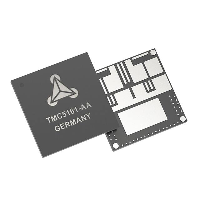


 工商网监
湘ICP备2023018690号
工商网监
湘ICP备2023018690号
