POWER DRIVER FOR BLDC/PMSM MOTORS
INTEGRATED CIRCUITS
TMC6100 DATASHEET
Universal high voltage BLDC/PMSM/Servo MOSFET 3-halfbridge gate-driver with up to 1.5A drive
current. Tiny QFN package with high creeping distance. External MOSFETs for up to 100A current.
APPLICATIONS
PMSM FOC drives and BLDC motors
Industrial Drives
Factory Automation
Lab Automation
Robotics
CNC machines
Textile Machines
Pumps
Surveillance Cameras
Home Automation
Printers
FEATURES
AND
BENEFITS
3-phase motors up to 100A coil current (external MOSFETs)
Voltage Range 8 … 60V DC
Gate Drive Programmable 0.5A / 1A / 1.5A
Full Protection and Diagnostics via SPI interface
Gate Off Drive with 1Ω (LS) / 1.3Ω (HS) safe hold off resistance
SPI & Stand-Alone operation
Charge Pump for 100% Duty Cycle operation
Optional BBM break-before-make logic for single line control
Programmable Short and Overload current threshold and retry
Programmable Control Interface with 3-line or 6-line drive
Full Protection & Diagnostics
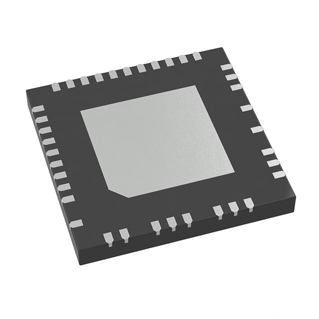
Compact Size 7x7mm2 QFN package
Double Pin Distance for safe operation at high voltage
BLOCK DIAGRAM
TRINAMIC Motion Control GmbH & Co. KG
Hamburg, Germany
DESCRIPTION
The TMC6100 is a high-power gate-driver
for PMSM servo or BLDC motors. Using
six external MOSFETs it controls motors
from Watt to Kilowatt. Software
controlled drive strength allows insystem EME optimization. Programmable
safety features like short detection and
overtemperature thresholds together
with an SPI interface for diagnostics
allow robust and reliable designs. With
the TMC6100, a minimum number of
external components is required to build
a rugged drive with full protection and
diagnostics.
�TMC6100 DATASHEET (Rev. 1.00 / 2019-NOV-14)
2
APPLICATION EXAMPLES: PMSM AND BLDC MOTORS
The TMC6100 is a compact driver IC for PMSM drivers. Its special package has sufficient creeping distance,
even for voltages of 48V. On the control side, it mates with sophisticated FOC TMC467x and TMC867x family
controller chips, or with any microcontroller. Its versatile interface matches simple BLDC drives with
minimum requirements on the µC PWM, as well as advanced PMSM control algorithms. The small form
factor of the TMC6100 keeps costs down and allows for miniaturized layouts. Extensive support at the chip,
board, and software levels enables rapid design cycles and fast time-to-market with competitive products.
High integration and reliability deliver cost savings in related systems such as power supplies and cooling.
MINIATURIZED CPU BASED DESIGN FOR BLDC OR PMSM
Gate CTRL
PWM
DIAG
High-Level
Interface
SPI
(optional)
CPU
TMC6100
ADC
M
Encoder
/ Hall
Current Sense
HIGH PERFORMANCE FOC SERVO DESIGN FOR PMSM
Gate CTRL
PWM
High-Level
Interface
CPU
SPI
TMC467x
ADC
Current
Sense
TMC6100
M
SPI
Encoder
/ Hall
A CPU with internal BLDC or sine wave PWM
unit drives the gate control lines based on
encoder or hall sensor feedback. External
current sensing is required, either using
simple Op AMPs for foot point sensing, or
series shunt amplifiers. Use of SPI is not
required,
unless
more
sophisticated
diagnostics is desired.
When using one of the TRINAMIC FOC
controllers, the CPU is completely offloaded
from time-intensive regulation loop tasks,
and software design shrinks to initialization
and target parameter setting. The TMC6100
optimally complements a TMC467x family
controller.
The TMC6100-EVAL is part of TRINAMICs
universal evaluation board system which
provides a convenient handling of the
hardware as well as a user-friendly
software tool for evaluation. The
TMC6100 evaluation board system
consists
of
three
parts:
LANDUNGSBRÜCKE
(base
board),
ESELSBRÜCKE (connector board including
several test points), and TMC6100-EVAL,
plus a TMC4671-EVAL FOC controller.
ORDER CODES
Order code
TMC6100-TA
TMC6100-TA-T
TMC6100-EVAL
LANDUNGSBRÜCKE
ESELSBRÜCKE
www.trinamic.com
PN
00-0201
00-0201-T
40-0197
40-0167
40-0098
Description
Three phase gate-driver for external MOSFETs; QFN 7x7
-T denotes tape on reel packed devices
Evaluation board for TMC6100.
Baseboard for TMC6100-EVAL and further boards.
Connector board for plug-in evaluation board system.
Size [mm2]
7x7
85 x 80
85 x 55
61 x 38
�TMC6100 DATASHEET (Rev. 1.00 / 2019-NOV-14)
3
Table of Contents
1
1.1
2
SPI DATAGRAM STRUCTURE .........................18
SPI SIGNALS ................................................19
TIMING .........................................................20
REGISTER MAPPING .......................................21
5.1
6
STANDARD APPLICATION CIRCUIT ................10
EXTERNAL GATE VOLTAGE REGULATOR ..........11
ZERO STANDBY CURRENT ..............................12
MOSFETS AND SLOPE CONTROL ..................13
TUNING THE MOSFET BRIDGE .....................15
SPI INTERFACE ................................................18
4.1
4.2
4.3
5
PACKAGE OUTLINE .......................................... 7
SIGNAL DESCRIPTIONS ................................... 7
SAMPLE CIRCUITS ..........................................10
3.1
3.2
3.3
3.4
3.5
4
CONTROL INTERFACES ..................................... 6
PIN ASSIGNMENTS ........................................... 7
2.1
2.2
3
8.1
8.2
PRINCIPLES OF OPERATION ......................... 4
GENERAL CONFIGURATION REGISTERS ..........22
DIAGNOSTICS AND PROTECTION .............27
6.1
6.2
TEMPERATURE SENSORS ................................27
SHORT PROTECTION ......................................27
7
EXTERNAL RESET .............................................29
8
CLOCK OSCILLATOR AND INPUT ...............29
www.trinamic.com
9
USING THE INTERNAL CLOCK ........................ 29
USING AN EXTERNAL CLOCK ......................... 29
ABSOLUTE MAXIMUM RATINGS ................. 30
10
10.1
10.2
10.3
11
11.1
11.2
11.3
11.4
11.5
12
12.1
12.2
ELECTRICAL CHARACTERISTICS ............ 30
OPERATIONAL RANGE ................................... 30
DC AND TIMING CHARACTERISTICS .............. 31
THERMAL CHARACTERISTICS.......................... 34
LAYOUT CONSIDERATIONS..................... 35
EXPOSED DIE PAD ........................................ 35
WIRING GND .............................................. 35
WIRING BRIDGE SUPPLY .............................. 35
SUPPLY FILTERING........................................ 35
LAYOUT EXAMPLE ......................................... 36
PACKAGE MECHANICAL DATA ................ 38
DIMENSIONAL DRAWINGS QFN7X7-EP ....... 38
PACKAGE CODES ........................................... 39
13
DISCLAIMER ................................................. 40
14
ESD SENSITIVE DEVICE............................ 40
15
DESIGNED FOR SUSTAINABILITY ......... 40
16
TABLE OF FIGURES .................................... 41
17
REVISION HISTORY ................................... 41
�TMC6100 DATASHEET (Rev. 1.00 / 2019-NOV-14)
1
4
Principles of Operation
The TMC6100 is a MOSFET gate driver for three phase PMSM and BLDC motors. Ideally suited for
applications in the range of 12V to 48V, it supports motor power ratings from 1 Watt to 1kW. It
complements with TRINAMICs TMC467x & TMC867x families of three phase motor controller ICs.
Internal break-before-make timing is provided for the ease-of-use in combination with simple
microcontrollers for PWM generation. A complete set of protection and diagnostic functions makes the
power stage more rugged than a discrete setup.
THE TMC6100 OFFERS TWO BASIC MODES OF OPERATION:
MODE 1: Stand-alone driver with pin configuration
Enable this mode by tying low pin SPE. The interface pins allow a number of different settings for
BBM generation.
MODE 2: SPI controlled
This mode allows detailed control over the protection, diagnostic and control features, e.g. for tuning
overcurrent detection. Enable this mode by tying high pin SPE.
100n
CE
VCP
Gate Voltage
Regulator
12VOUT
Charge Pump
CU
12VOUT
4.7µ
HS
5VOUT
470n
IT
VSA
100n
100n
16V
VS
22n
100V
VCP
+VM
CPI
CPO
+VM
CB
HSU
U
5V Regulator
2.2µ
3.3V or 5V +VIO
I/O voltage
VCC_IO
pd
UL
pd
VH
pd
VL
pd
WH
pd
WL
pd
B.Dwersteg, ©
TRINAMIC 2014
Break before
Make logic
VCP
HS
+VIO
LS
www.trinamic.com
LSV
CW
HS
HSW
W
LS
pd
Enable
Figure 1.1 Standalone application
HSV
N
Configuration
interface
0
3 Phase
Motor
CB
S
DIE PAD
1
External Sense
amplifier
V
12VOUT
DRV_EN
0: xH/xL individual gate control
1: xH=Polarity, xL=Enable control
CSN / IDRV0
SCK / IDRV1
SDI
SDO / SINGLE
Diagnostics
(Short circuit,
Temperature)
SPE
Driver Strength [IDRV1 IDRV0]:
00: 0.5A 01: 0.5/1A, 10: 1A, 11: 1.5A
FAULT
CV
12VOUT
VCP
Diagnostic Output
RS
IT
Chopper Control
dual line LS+HS,
or single line
(HS=polarity, LS=enable)
24MHz Oscillator
UH
GNDA
CLK_IN
TMC6100
OTP memory
LSU
IT
LS
100n
LSW
CB
RS
External Sense
amplifier
�TMC6100 DATASHEET (Rev. 1.00 / 2019-NOV-14)
5
100n
CE
VSA
VCP
Gate Voltage
Regulator
12VOUT
100n
Charge Pump
CU
12VOUT
4.7µ
HS
5VOUT
470n
IT
100n
16V
VS
22n
100V
VCP
+VM
CPI
CPO
+VM
CB
HSU
U
5V Regulator
2.2µ
3.3V or 5V +VIO
I/O voltage
VCC_IO
OTP memory
UL
pd
VH
pd
VL
pd
WH
pd
WL
pd
B.Dwersteg, ©
TRINAMIC 2014
Break before
Make logic
HS
N
LS
CW
12VOUT
HS
Configuration
interface
LS
0
CB
HSW
LSW
5VOUT
SPE
+VIO
DIE PAD
pd
DRV_EN
1
LSV
W
CSN / IDRV0
SCK / IDRV1
SDI
SDO / SINGLE
0: xH/xL individual gate control
1: xH=Polarity, xL=Enable control
HSV
S
VCP
Driver Strength [IDRV1 IDRV0]:
00: 0.5A 01: 0.5/1A, 10: 1A, 11: 1.5A
3 Phase
Motor
CB
V
Diagnostics
(Short circuit,
Temperature)
FAULT
Diagnostic Output
CV
12VOUT
IT
pd
Current Sense
GNDA
Chopper Control
dual line LS+HS,
or single line
(HS=polarity, LS=enable)
24MHz Oscillator
UH
VCP
TMC6100
CLK_IN
LSU
IT
LS
100n
RS
R1
R2
Use LMV641 or similar
Amplification=1+R2/R1
Enable
Figure 1.2 Standalone application using single shunt current sensing
100n
VSA
Gate Voltage
Regulator
12VOUT
100n
CE
VCP
Charge Pump
HS
5VOUT
5V Regulator
IW
VCC_IO
UH
UL
pd
VH
pd
VL
pd
WH
pd
WL
pd
B.Dwersteg, ©
TRINAMIC 2014
Break before
Make logic
VCP
SPI
CSN / IDRV0
SCK / IDRV1
SDI
SDO / SINGLE
Diagnostics
(Short circuit,
Temperature)
CV
12VOUT
HS
N
S
LS
HS
HSW
SPI interface
LS
Figure 1.3 SPI mode configuration
GNDA
DIE PAD
DRV_EN
SPE
pd
www.trinamic.com
LSV
CW
12VOUT
Enable
3 Phase
Motor
CB
HSV
W
+VIO
External Sense
amplifier
V
VCP
FAULT
RS
IT
TMC6100
24MHz Oscillator
pd
LSU
IT
LS
OTP memory
Chopper Control
dual line LS+HS,
or single line
(HS=polarity, LS=enable)
USENSE
+
100n
CLK_IN
CB
HSU
U
VOFS
2.2µ
3.3V or 5V +VIO
I/O voltage
CU
12VOUT
4.7µ
470n
IT
100n
16V
VS
22n
100V
VCP
+VM
CPI
CPO
+VM
LSW
CB
RS
External Sense
amplifier
�TMC6100 DATASHEET (Rev. 1.00 / 2019-NOV-14)
6
1.1 Control Interfaces
The TMC6100 supports six control lines for the MOSFET drivers. High-side and low-side outputs can be
individually controlled, or by an individual enable pin plus polarity pin, using internal BBM circuitry.
An SPI interface or standalone configuration is supported.
1.1.1
Standalone Configuration
Standalone configuration covers the most important settings like driver current and current amplifier
amplification factor and the selection of internal or external BBM operation using four pins. Additional
settings like BBM time and sensitivity of short detection can be modified using pre-programming via
OTP memory, e.g. via an initial programming during product testing. This way, the driver can be fully
operated and all protection mechanisms are in place. The fault output signals any critical driver error.
It becomes cleared by disabling / re-enabling the driver.
However, no advanced debugging is possible, like individual testing of failure mechanisms or setting
a more sensitive temperature threshold.
Hint
Standalone configuration is recommended for low-cost applications with small motors (e.g. motor
current up to 10A RMS), where advanced debugging is not required or not possible. In case a
sensitive overtemperature threshold must be set, the SPI interface should be used.
1.1.2
SPI Interface
The SPI interface is a bit-serial interface synchronous to a bus clock. For every bit sent from the bus
master to the bus slave another bit is sent simultaneously from the slave to the master.
Communication between an SPI master and the TMC6100 slave always consists of sending one 40-bit
command word and receiving one 40-bit status word.
The SPI command rate typically is a few commands for initialization or for diagnostic feedback.
Attention
When operating in SPI mode, set drive mode (single line or individual control signals) first. For safety
reasons, the driver starts up in single line mode. Note, that this setting will prevent operation if a
controller operates the IC using individual control signals. Therefore, initialize the control mode first.
www.trinamic.com
�TMC6100 DATASHEET (Rev. 1.00 / 2019-NOV-14)
2
7
Pin Assignments
CU
HSU
U
CV
HSV
V
W
HSW
CW
37
36
35
34
33
32
31
30
2.1 Package Outline
1
19
20
21
WL
CLK
10
WH
CSN_IDRV0
PAD = GNDP, GNDD
18
9
VL
TEST
17
8
VH
GNDA
16
7
VCC_IO
5VOUT
15
6
UL
12VOUT
14
5
UH
LSU
TMC6100-LA
QFN7x7
13
4
SDO_SINGLE
LSV
VCP
28
VS
27
CPI
26
CPO
25
VSA
24
DRV_EN
23
FAULT
22
SPE
Bernhard Dwersteg, TRINAMIC
12
3
SDI
LSW
11
2
SCK_IDRV1
-
29
Figure 2.1 TMC6100-LA pinning QFN 37 special (7x7mm²)
2.2 Signal Descriptions
Pin
QFN
CU
1
LSW
LSV
LSU
2
3
4
5
www.trinamic.com
Type
N.C.
Function
Bootstrap capacitor positive connection. Tie to U terminal
using 470nF to 1µF, 16V or 25V ceramic capacitor.
Unused pin (may be tied to GND)
Low side gate driver output.
Low side gate driver output.
Low side gate driver output.
�TMC6100 DATASHEET (Rev. 1.00 / 2019-NOV-14)
Pin
QFN
Type
12VOUT
6
5VOUT
7
GNDA
TEST
8
9
AI
CSN_IDRV0
10
DI
SCK_IDRV1
11
DI
SDI
12
DI
SDO_SINGLE
13
DIO
UH
14
UL
15
VCC_IO
16
DI
(pd)
DI
(pd)
DI
(pd)
DI
(pd)
DI
(pd)
DI
(pd)
VH
17
VL
18
WH
19
WL
20
CLK
21
DI
SPE
22
DI
(pd)
FAULT
23
DO
DRV_EN
24
DI
VSA
25
CPO
26
CPI
27
VS
28
VCP
29
www.trinamic.com
Function
Output of internal 11.5V gate voltage regulator and supply pin
of low side gate drivers. Attach 2.2µF to 22µF ceramic
capacitor to GND plane near to pin for best performance. Use
at least 5-10 times more capacity than for bootstrap capacitors.
In case an external gate voltage supply is available, tie VSA
and 12VOUT to the external supply.
Output of internal 5V regulator. Attach 2.2µF to 10µF ceramic
capacitor to GNDA near to pin for best performance.
Analog GND. Connect to GND plane near pin.
leave open
SPI chip select input (negative active) (SPE=1) or
Configuration input for gate driver current LSB (SPE=0)
SPI serial clock input (SPE=1) or
Configuration input for gate driver current MSB (SPE=0)
SPI data input
SPI data output (tristate) (SPE=1) or
Configuration input for internal bridge control mode (0: dual
line, 1: xH=phase polarity, xL=phase enable) (SPE=0)
High side control input (or bridge polarity in single mode)
Low side control input (or bridge enable in single mode)
3.3V to 5V IO supply voltage for all digital pins.
High side control input (or bridge polarity in single mode)
Low side control input (or bridge enable in single mode)
High side control input (or bridge polarity in single mode)
Low side control input (or bridge enable in single mode)
CLK input. Tie to GND using short wire for internal clock or
supply external clock. Internal clock-fail over circuit protects
against loss of external clock signal.
Mode selection input. When tied low, the chip is in standalone
mode and SPI pins have their configuration pin functions.
When tied high, the SPI interface is enabled. Integrated pull
down resistor.
Diagnostics output.
High upon driver error condition. Clear by cycling EN.
Positive active enable input. The power stage becomes
switched off (all motor outputs floating) when this pin
becomes driven to a low level. Cycle low to clear FAULT.
Analog supply voltage for 11.5V and 5V regulator. Normally
tied to VS. Provide a 100nF filtering capacitor to GND.
Charge pump capacitor output.
Charge pump capacitor input. Tie to CPO using 22nF 100V
capacitor. In case ringing of the power supply leads to
considerable supply ripple, add a 10-22Ohm series resistor.
Motor supply voltage. Provide filtering capacity near pin with
short loop to GND plane. Must be tied to the positive bridge
supply voltage. Severe ringing must be avoided.
Charge pump voltage. Tie to VS using 100nF capacitor.
8
�TMC6100 DATASHEET (Rev. 1.00 / 2019-NOV-14)
Pin
QFN
CW
30
HSW
31
W
32
V
33
HSV
34
CV
35
U
36
HSU
37
Exposed die pad
-
Type
Function
Bootstrap capacitor positive connection. Tie to W terminal
using 470nF to 1µF, 16V or 25V ceramic capacitor.
High side gate driver output.
Bridge center and bootstrap capacitor negative connection.
Connect to source pin of HS-MOSFET.
Bridge center and bootstrap capacitor negative connection.
Connect to source pin of HS-MOSFET.
High side gate driver output.
Bootstrap capacitor positive connection. Tie to V terminal
using 470nF to 1µF, 16V or 25V ceramic capacitor.
Bridge center and bootstrap capacitor negative connection.
Connect to source pin of HS-MOSFET.
High side gate driver output.
Connect the exposed die pad to a GND plane. Provide as many
as possible vias for heat transfer to GND plane. Serves as GND
pin for the low side gate drivers and for digital logic. Ensure
low loop inductivity to bridge GND.
*(pd) denominates a pin with pulldown resistor
www.trinamic.com
9
�TMC6100 DATASHEET (Rev. 1.00 / 2019-NOV-14)
3
10
Sample Circuits
The following sample circuits show the required external components in different operation and
supply modes. The connection of the external current amplifier, bus interface and further digital
signals are left out for clarity.
3.1 Standard Application Circuit
+VM
100n
CE
VCP
Gate Voltage
Regulator
12VOUT
Charge Pump
HS
5VOUT
CB
CU
12VOUT
4.7µ
470n
IT
VSA
100n
100n
16V
VS
22n
100V
VCP
+VM
CPI
CPO
Optional use lower
voltage down to 12V
RG
U
5V Regulator
Use low inductivity SMD
type resistors!
HSU
2.2µ
3.3V or 5V +VIO
I/O voltage
VCC_IO
LS
100n
LSU
RS
TMC6100
24MHz Oscillator
UH
pd
UL
pd
VH
pd
VL
pd
WH
pd
WL
pd
B.Dwersteg, ©
TRINAMIC 2014
Break before
Make logic
VCP
HS
Diagnostics
(Short circuit,
Temperature)
N
S
LS
LSV
CW
12VOUT
HS
CB
RS
HSW
SPI interface
LS
LSW
RG
+VIO
+VIO
Driver Enable
(positive active)
GNDA
GND: Stand alone,
VIO: SPI interface mode
DIE PAD
pd
External Sense
amplifier
RG
W
DRV_EN
0: xH/xL individual gate control
1: xH=Polarity, xL=Enable control
RG
RG
SPE
Driver Strength [IDRV1 IDRV0]:
00: 0.5A 01: 0.5/1A, 10: 1A, 11: 1.5A
FAULT
SPI interface
(SPE=1)
CSN / IDRV0
SCK / IDRV1
SDI
SDO / SINGLE
HSV
V
VCP
Settings in Standalone
mode (SPE=0)
3 Phase
Motor
CB
CV
12VOUT
IT
CLK_IN
External Sense
amplifier
IT
RG
OTP memory
Keep inductivity of the fat
interconnections as small as
possible to avoid undershoot
of U/V/W < -5V!
Bootstrap capacitors CB:
For MOSFETs with QG10Ohm
Figure 3.10 Diodes for safe off condition with high gate series resistance
BRIDGE LAYOUT CONSIDERATIONS
-
-
Tune the bridge layout for minimum loop inductivity. A compact layout is best.
Keep MOSFET gate connections short and straight and avoid loop inductivity between bridge
feedback (U,V,W) and corresponding HS driver pin. Loop inductance is minimized with parallel
traces, or adjacent traces on adjacent layers. A wider trace reduces inductivity (don’t use minimum
trace width).
Place the TMC6100 near the low side MOSFETs GND connections, with its GND connections directly
connected to the same GND plane.
Optimize switching behavior by using lowest acceptable gate current setting.
Check influence of optional components shown in Figure 3.6.
Measure the performance of the bridge by probing BM pins directly at the bridge or at the
TMC6100 using a short GND tip on the scope probe rather than a GND cable, if available.
www.trinamic.com
�TMC6100 DATASHEET (Rev. 1.00 / 2019-NOV-14)
4
18
SPI Interface
4.1 SPI Datagram Structure
The TMC6100 uses 40 bit SPI™ (Serial Peripheral Interface, SPI is Trademark of Motorola) datagrams
for communication with a microcontroller. Microcontrollers which are equipped with hardware SPI are
typically able to communicate using integer multiples of 8 bit. The NCS line of the device must be
handled in a way, that it stays active (low) for the complete duration of the datagram transmission.
Each datagram sent to the device is composed of an address byte followed by four data bytes. This
allows direct 32 bit data word communication with the register set. Each register is accessed via 32
data bits even if it uses less than 32 data bits.
For simplification, each register is specified by a one-byte address:
- For a read access the most significant bit of the address byte is 0.
- For a write access the most significant bit of the address byte is 1.
Read and write functionality of the individual registers may differ.
SPI DATAGRAM STRUCTURE
MSB (transmitted first)
40 bit
39 ...
→ 8 bit address
8 bit SPI status
... 0
→ 32 bit data
39 ... 32
→ to TMC6100
RW + 7 bit address
from TMC6100
unused
W
39 / 38 ... 32
38...32
LSB (transmitted last)
31 ... 0
8 bit data
8 bit data
31 ... 24
31...28
27...24
23 ... 16
23...20
19...16
8 bit data
8 bit data
15 ... 8
15...12
7 ... 0
11...8
7...4
3...0
3 3 3 3 3 3 3 3 3 3 2 2 2 2 2 2 2 2 2 2 1 1 1 1 1 1 1 1 1 1
9 8 7 6 5 4 3 2 1 0
9 8 7 6 5 4 3 2 1 0 9 8 7 6 5 4 3 2 1 0 9 8 7 6 5 4 3 2 1 0
4.1.1
Selection of Write / Read (WRITE_notREAD)
The read and write selection is controlled by the MSB of the address byte (bit 39 of the SPI
datagram). This bit is 0 for read access and 1 for write access. So, the bit named W is a
WRITE_notREAD control bit. The active high write bit is the MSB of the address byte. So, 0x80 has to
be added to the address for a write access. The SPI interface always delivers data back to the master,
independent of the W bit. Read data coming back in a write access should be ignored.
Read data is transferred back to the master directly in the read access. Internal read access occurs
during the transmission in the moment when the address bits have been received.
Example:
For a read access to the register (GSTAT) with the address 0x00, the address byte has to be
set to 0x00. For a write access to the register (GCONF), the address byte has to be set to
0x80 + 0x01 = 0x81. For read access, the data bits don’t care. So, one can set them to 0.
action
read GSTAT
write GCONF:= 0x00000010
data sent to TMC6100
→ 0x0100000000
→ 0x8000000010
data received from TMC6100
AA & GSTAT
0x01 & unused
*)AA: is a placeholder for the address byte used in the previous access
www.trinamic.com
�TMC6100 DATASHEET (Rev. 1.00 / 2019-NOV-14)
4.1.2
19
Data Alignment
All data are right aligned. Some registers represent unsigned (positive) values, some represent integer
values (signed) as two’s complement numbers, single bits or groups of bits are represented as single
bits respectively as integer groups.
4.2 SPI Signals
The SPI bus on the TMC6100 has four signals:
- SCK – bus clock input
- SDI – serial data input
- SDO – serial data output
- CSN – chip select input (active low)
The slave is enabled for an SPI transaction by a low on the chip select input CSN. Bit transfer is
synchronous to the bus clock SCK, with the slave latching the data from SDI on the rising edge of SCK
and driving data to SDO following the falling edge. The most significant bit is sent first. A minimum
of 40 SCK clock cycles is required for a bus transaction with the TMC6100.
The TMC6100 does not allow cascading of SPI slaves. Use individual CSN lines for each device.
CSN must be low during the whole bus transaction. When CSN goes high, the contents of the internal
shift register are latched into the internal control register and recognized as a command from the
master to the slave.
www.trinamic.com
�TMC6100 DATASHEET (Rev. 1.00 / 2019-NOV-14)
20
4.3 Timing
The SPI interface is synchronized to the internal system clock, which limits the SPI bus clock SCK to
1/4 of the system clock frequency. If the system clock is based on the on-chip oscillator, an additional
10% safety margin must be used to ensure reliable data transmission. All SPI inputs as well as the
ENN input are internally filtered to avoid triggering on pulses shorter than 20ns. Figure 4.1 shows the
timing parameters of an SPI bus transaction, and the table below specifies their values.
CSN
tCC
tCL
tCH
tCH
tCC
SCK
tDU
SDI
bit39
tDH
bit38
bit0
tDO
SDO
tZC
bit39
bit38
bit0
Figure 4.1 SPI timing
Hint
Usually this SPI timing is referred to as SPI MODE 3
SPI interface timing
Parameter
SCK valid before or after change
of CSN
AC-Characteristics
clock period: tCLK
Symbol
tCC
fSCK
fSCK
assumes
synchronous CLK
tCSH
SCK low time
tCL
SCK high time
tCH
www.trinamic.com
Min
Typ
Max
10
*) Min time is for
synchronous CLK
with SCK high one
tCH before CSN high
only
*) Min time is for
synchronous CLK
only
*) Min time is for
synchronous CLK
only
assumes minimum
OSC frequency
CSN high time
SCK frequency using internal
clock
SCK frequency using external
clock
SDI setup time before rising
edge of SCK
SDI hold time after rising edge
of SCK
Data out valid time after falling
SCK clock edge
SDI, SCK and CSN filter delay
time
Conditions
Unit
ns
tCLK*)
>2tCLK+10
ns
tCLK*)
>tCLK+10
ns
tCLK*)
>tCLK+10
ns
3.5
MHz
fCLK/6
MHz
tDU
10
ns
tDH
10
ns
tDO
no capacitive load
on SDO
tFILT
rising and falling
edge
12
20
tCLK+10
ns
30
ns
�TMC6100 DATASHEET (Rev. 1.00 / 2019-NOV-14)
5
21
Register Mapping
This chapter gives an overview of the complete register set. Some of the registers bundling a number
of single bits are detailed in extra tables. The functional practical application of the settings is detailed
in dedicated chapters.
Note
- All registers become reset to 0 upon power up, unless otherwise noted.
- Add 0x80 to the address Addr for a write access!
NOTATION OF HEXADECIMAL AND BINARY NUMBERS
0x
%
precedes a hexadecimal number, e.g. 0x04
precedes a multi-bit binary number, e.g. %100
NOTATION OF R/W FIELD
R
W
R/W
R+WC
Read only
Write only
Read- and writable register
Clear upon write back with ‘1’
OVERVIEW REGISTER MAPPING
REGISTER
DESCRIPTION
General Configuration Registers
These registers contain
global configuration
global status flags
interface configuration
driver configuration
OTP programming
www.trinamic.com
�TMC6100 DATASHEET (Rev. 1.00 / 2019-NOV-14)
22
5.1 General Configuration Registers
GENERAL CONFIGURATION REGISTERS (0X00…0X0F)
R/W
Addr
n
RW
0x00
17
R+
WC
0x01
15
www.trinamic.com
Register
GCONF
GSTAT
Description / bit names
Bit
GCONF – Global configuration flags
0 disable: Driver Disable
1:
Disable driver (e.g. for Resetting of short
condition)
1 singleline: Interface mode (reset default = 1)
0:
Individual signals L+H
1:
H-Input is control signal, L-Input is Enable
2 faultdirect
0:
Fault output active when at least one bridge is
shut down continuously due to overcurrent or
overtemperature
1:
Fault output shows each protective action of the
overcurrent shutdown
5:3 unused
6 1:
Normal operation - set upon write access for
reduced power consumption
7 test_mode
0:
Normal operation
1:
Enable analog test output on pin DRV_EN.
BBM_CLKS[1..0] selects the function of DRV_EN:
0…2: T120, DAC, VDDH
Attention: Not for user, set to 0 for normal operation!
31:8 unused
Bit
GSTAT – Global status flags
(Re-Write with ‘1’ bit to clear respective flags, or cycle
DRV_EN to clear all bits except for reset and drv_otpw)
Attention: Switch off the affected MOSFET by its HS/LS
input in order to clear a pending short condition. Just
resetting the flag will not switch it on again.
0 reset
1:
Indicates that the IC has been reset. All registers
have been cleared to reset values.
Attention: DRV_EN must be high to allow clearing reset
1 drv_otpw
1:
Indicates, that the driver temperature has
exceeded overtemperature prewarning-level. No
action is taken. This flag is latched.
2 drv_ot
1:
Indicates, that the driver has been shut down
due to overtemperature. This flag can only be
cleared when the temperature is below the limit
again. It is latched for information.
ORed to STATUS output.
3 uv_cp
1:
Indicates an undervoltage on the charge pump.
The driver is disabled during undervoltage. This
flag is latched for information.
ORed to STATUS output.
4 shortdet_u
1:
U short counter has triggered at least once.
ORed to STATUS output.
�TMC6100 DATASHEET (Rev. 1.00 / 2019-NOV-14)
23
GENERAL CONFIGURATION REGISTERS (0X00…0X0F)
R/W
Addr
n
Register
Description / bit names
5 s2gu
1:
Short to GND detected on phase U. The driver
becomes disabled until flag becomes cleared.
ORed to STATUS output.
6 s2vsu
1:
Short to VS detected on phase U. The driver
becomes disabled until flag becomes cleared.
ORed to STATUS output.
7 8
9
10
11
12
13
14
Bit
R
W
0x04
8
+
8
0x06
www.trinamic.com
IOIN
OTP_PROG
0
1
2
3
4
5
6
7
8
9
10
11
31..
24
Bit
shortdet_v
1:
V short counter has triggered at least once.
ORed to STATUS output.
s2gv
1:
Short to GND detected on phase V. The driver
becomes disabled until flag becomes cleared.
ORed to STATUS output.
s2vsv
1:
Short to VS detected on phase V. The driver
becomes disabled until flag becomes cleared.
ORed to STATUS output.
shortdet_w
1:
short counter has triggered at least once.
ORed to STATUS output.
s2gw
1:
Short to GND detected on phase W. The driver
becomes disabled until flag becomes cleared.
ORed to STATUS output.
s2vsw
1:
Short to VS detected on phase W. The driver
becomes disabled until flag becomes cleared.
ORed to STATUS output.
INPUT
Reads the state of all input pins available
UL
UH
VL
VH
WL
WH
DRV_EN
0
OTPW
OT136°C
OT143°C
OT150°C
VERSION: 0x10=first version of the IC
Identical numbers mean full digital compatibility.
OTP_PROGRAM – OTP programming
Write access programs OTP memory (one bit at a time),
�TMC6100 DATASHEET (Rev. 1.00 / 2019-NOV-14)
24
GENERAL CONFIGURATION REGISTERS (0X00…0X0F)
R/W
Addr
n
Register
R
0x07
RW
0x08
5
FACTORY_
CONF
RW
0x09
19
SHORT_
CONF
OTP_READ
www.trinamic.com
Description / bit names
Read access refreshes read data from OTP after a write
2..0 OTPBIT
Selection of OTP bit to be programmed to the selected
byte location (n=0..7: programs bit n to a logic 1)
5..4 OTPBYTE
Set to 00
15..8 OTPMAGIC
Set to 0xbd to enable programming. A programming
time of minimum 10ms per bit is recommended (check
by reading OTP_READ).
Bit
OTP_READ (Access to OTP memory result and update)
See table 5.1.1!
7..0 OTP0 byte 0 read data
4..0 FCLKTRIM (Reset default: OTP)
0…31: Lowest to highest clock frequency. Check at
charge pump output. The frequency span is not
guaranteed, but it is tested, that tuning to 12MHz
internal clock is possible. The devices come preset to
12MHz clock frequency by OTP programming.
(Reset Default: OTP)
Bit
SHORT_CONF
3..0 S2VS_LEVEL:
Short to VS detector level for lowside FETs. Checks for
voltage drop in LS MOSFET and bottom shunt resistor.
1 (highest sensitivity) … 15 (lowest sensitivity)
(Reset Default: OTP 6 or 12)
11..8 S2G_LEVEL:
Short to GND detector level for highside FETs. Checks
for voltage drop on high side MOSFET
2 (highest sensitivity) … 15 (lowest sensitivity)
Hint: Use high setting. Tune S2VS level for more
sensitive overcurrent detection.
(Reset Default: OTP 6 or 12)
17..16 SHORTFILTER:
Spike filtering bandwidth for short detection
0 (lowest, 100ns), 1 (1µs), 2 (2µs) 3 (3µs)
Hint: Increase value, if erroneous short detection
occurs.
(Reset Default = %01)
20 shortdelay: Short detection delay
0=750ns: normal, 1=1500ns: high
The short detection delay shall cover the bridge
switching time. 0 will work for most applications.
(Reset Default = 0)
25..24 RETRY: Number of retries for short detection
0:
Half bridge disabled after first short detection
1..3: Half bridge re-enabled in next chopper cycles 1
time to 3 times. With retry, the short-counter is
decreased once each 256 chopper cycles per coil,
unless the upper limit has been reached.
(Reset Default = 3)
�TMC6100 DATASHEET (Rev. 1.00 / 2019-NOV-14)
25
GENERAL CONFIGURATION REGISTERS (0X00…0X0F)
R/W
Addr
n
Register
Description / bit names
28 protect_parallel
0:
Only the detected half bridge driver becomes
shut down upon final short detection
1:
All half bridge drivers become shut down upon
final short detection
(Reset Default = 1)
29
30
Bit
4..0
15:5
17..16
RW
0x0A
22
DRV_CONF
19..18
31:20
www.trinamic.com
disable_S2G
0:
Short to GND (HS) protection enabled
1:
No short to GND protection
(Reset Default = 0)
disable_S2VS
0:
Short to VS (LS) protection enabled
1:
No short to VS protection
(Reset Default = 0)
DRV_CONF
BBMCLKS:
0..15: Digital BBM time in clock cycles (typ. 42ns/CLK).
BBMCLKS is used in combination with singleline=1. It is
not applicable with individual LS and HS signals.
(Reset Default: OTP 1..4)
unused
OTSELECT:
Selection of over temperature level for bridge disable,
switch on after cool down to 120°C / OTPW level.
00: 150°C (default)
01: 143°C
10: 136°C
11: 120°C (not recommended, no hysteresis)
Hint: Adapt overtemperature threshold as required to
protect the MOSFETs or other components on the PCB.
(Reset Default = %00)
DRVSTRENGTH:
Selection of gate driver current. Adapts the gate driver
current to the gate charge of the external MOSFETs.
00: weak
01: weak+TC (medium above OTPW level)
10: medium
11: strong
Hint: Choose the lowest setting giving slopes


 工商网监
湘ICP备2023018690号
工商网监
湘ICP备2023018690号


