INTEGRATED CIRCUITS
EtherCAT Slave Controller for
TMC8462 Datasheet
Document Revision V1.5 • 2019-June-21
The TMC8462 is a complete EtherCAT® Slave Controller optimized for real time. It comprises all
blocks required for an EtherCAT slave including two 100-Mbit PHYs, a dual switch regulator power
supply and 24V capable high voltage I/Os for industrial environments. Timer, watchdog, PWM
and SPI/IIC master units allow for enhanced capabilities either in device emulation mode or in
combination with an external CPU.
Features
• Standard compliant EtherCAT® Slave
• Dual Integrated 100-Mbit Ethernet
PHY
• SPI Process Data Interface (PDI)
• IO Block with 24 Multi-Function I/Os
• Internal 3.3V plus free 5V-24V switch
regulator
• 8 High Voltage I/Os (up to 35V, 100mA)
• Multifunction block comprises Watchdog, 4 PWM outputs and Step/Dir
generator
• Direct EtherCAT access to external
ADCs, stepper motor controllers, etc.
• EtherCAT-P compatible voltage range
Applications
• Factory Automation
• Process Automation
• Communication Modules
• Industrial IoT
• Industry 4.0
• Sensors & Encoders
Simplified Block Diagram
©2019 TRINAMIC Motion Control GmbH & Co. KG, Hamburg, Germany
Terms of delivery and rights to technical change reserved.
Download newest version at: www.trinamic.com
Read entire documentation.
• Robotics
• Industrial Motion Control
• Building Automation
�2 / 204
TMC8462 Datasheet • Document Revision V1.5 • 2019-June-21
Contents
1
Product Features
5
2
Order Codes
6
3
Principles of Operation / Key Concepts
3.1 General Device Architecture . . . . .
3.2 EtherCAT Slave Controller . . . . . . .
3.3 Multi-Function and Control IO Block .
3.4 Analog and High Voltage Block . . . .
3.5 Interfaces . . . . . . . . . . . . . . . .
3.6 Software- and Tool-Support . . . . .
.
.
.
.
.
.
.
.
.
.
.
.
.
.
.
.
.
.
.
.
.
.
.
.
.
.
.
.
.
.
.
.
.
.
.
.
.
.
.
.
.
.
.
.
.
.
.
.
.
.
.
.
.
.
.
.
.
.
.
.
.
.
.
.
.
.
.
.
.
.
.
.
.
.
.
.
.
.
.
.
.
.
.
.
.
.
.
.
.
.
.
.
.
.
.
.
.
.
.
.
.
.
.
.
.
.
.
.
.
.
.
.
.
.
.
.
.
.
.
.
.
.
.
.
.
.
.
.
.
.
.
.
.
.
.
.
.
.
.
.
.
.
.
.
.
.
.
.
.
.
.
.
.
.
.
.
.
.
.
.
.
.
.
.
.
.
.
.
.
.
.
.
.
.
.
.
.
.
.
.
.
.
.
.
.
.
.
.
.
.
.
.
7
. 7
. 8
. 8
. 9
. 10
. 10
4
Device Pin Definitions
15
4.1 Pinout and Pin Coordinates of TMC8462-BA . . . . . . . . . . . . . . . . . . . . . . . . . . . . . 15
4.2 Signal Descriptions . . . . . . . . . . . . . . . . . . . . . . . . . . . . . . . . . . . . . . . . . . . . 15
5
Device Usage and Handling
5.1 Process Data Interface . . . . . . . . . . . . . . . . . . . . . . . .
5.1.1 SPI protocol description . . . . . . . . . . . . . . . . . . .
5.1.2 Timing example . . . . . . . . . . . . . . . . . . . . . . . .
5.2 MFC IO Control Interface . . . . . . . . . . . . . . . . . . . . . . .
5.2.1 SPI Protocol description . . . . . . . . . . . . . . . . . . .
5.2.2 Timing example . . . . . . . . . . . . . . . . . . . . . . . .
5.2.3 Sharing Bus Lines with the PDI SPI . . . . . . . . . . . . .
5.3 Ethernet Physical Layer Connection . . . . . . . . . . . . . . . . .
5.4 External Circuitry and Applications Examples . . . . . . . . . . .
5.4.1 Device Reset . . . . . . . . . . . . . . . . . . . . . . . . . .
5.4.2 Supply Filtering for PLL Supply . . . . . . . . . . . . . . .
5.4.3 PHY Power Regulator Filtering . . . . . . . . . . . . . . . .
5.4.4 External Circuit for Fixed Switching Regulator 0 . . . . . .
5.4.5 External Circuit for Adjustable Switching Regulator 1 . .
5.4.6 Minimum External Supply Circuit for Single 3.3V Supply .
5.4.7 Minimum External Supply Circuit for Single 5V Supply . .
5.4.8 Minimum External Supply Circuit for Single Supply >5V .
5.4.9 Typical Power Supply Chain Using Both Buck Converters
5.4.10 Status LED Circuit . . . . . . . . . . . . . . . . . . . . . . .
5.4.11 SII EEPROM Circuit . . . . . . . . . . . . . . . . . . . . . . .
5.4.12 Considerations on PHY to PHY Connection . . . . . . . .
.
.
.
.
.
.
.
.
.
.
.
.
.
.
.
.
.
.
.
.
.
.
.
.
.
.
.
.
.
.
.
.
.
.
.
.
.
.
.
.
.
.
.
.
.
.
.
.
.
.
.
.
.
.
.
.
.
.
.
.
.
.
.
.
.
.
.
.
.
.
.
.
.
.
.
.
.
.
.
.
.
.
.
.
.
.
.
.
.
.
.
.
.
.
.
.
.
.
.
.
.
.
.
.
.
.
.
.
.
.
.
.
.
.
.
.
.
.
.
.
.
.
.
.
.
.
.
.
.
.
.
.
.
.
.
.
.
.
.
.
.
.
.
.
.
.
.
.
.
.
.
.
.
.
.
.
.
.
.
.
.
.
.
.
.
.
.
.
.
.
.
.
.
.
.
.
.
.
.
.
.
.
.
.
.
.
.
.
.
.
.
.
.
.
.
.
.
.
.
.
.
.
.
.
.
.
.
.
.
.
.
.
.
.
.
.
.
.
.
.
.
.
.
.
.
.
.
.
.
.
.
.
.
.
.
.
.
.
.
.
.
.
.
.
.
.
.
.
.
.
.
.
.
.
.
.
.
.
.
.
.
.
.
.
.
.
.
.
.
.
.
.
.
.
.
.
.
.
.
.
.
.
.
.
.
.
.
.
.
.
.
.
.
.
.
.
.
.
.
.
.
.
.
.
.
.
.
.
.
.
.
.
.
.
.
.
.
.
.
.
.
.
.
.
.
.
.
.
.
.
.
.
.
.
.
.
.
.
.
.
.
.
.
.
.
.
.
.
.
.
.
.
.
.
.
.
.
23
23
24
26
27
27
28
28
30
31
31
31
32
33
34
35
36
37
38
38
38
39
EtherCAT Slave Controller Description
6.1 General EtherCAT Information . . . .
6.2 Overview of Available Chip Features
6.3 EtherCAT Register Overview . . . . .
6.4 EtherCAT Register Set . . . . . . . . .
6.4.1 ESC Information . . . . . . . .
6.4.2 Station Address . . . . . . . .
6.4.3 Write Protection . . . . . . . .
6.4.4 Data Link Layer . . . . . . . .
6.4.5 Application Layer . . . . . . .
6.4.6 PDI . . . . . . . . . . . . . . . .
6.4.7 Interrupts . . . . . . . . . . . .
6.4.8 Error Counters . . . . . . . . .
.
.
.
.
.
.
.
.
.
.
.
.
.
.
.
.
.
.
.
.
.
.
.
.
.
.
.
.
.
.
.
.
.
.
.
.
.
.
.
.
.
.
.
.
.
.
.
.
.
.
.
.
.
.
.
.
.
.
.
.
.
.
.
.
.
.
.
.
.
.
.
.
.
.
.
.
.
.
.
.
.
.
.
.
.
.
.
.
.
.
.
.
.
.
.
.
.
.
.
.
.
.
.
.
.
.
.
.
.
.
.
.
.
.
.
.
.
.
.
.
.
.
.
.
.
.
.
.
.
.
.
.
.
.
.
.
.
.
.
.
.
.
.
.
.
.
.
.
.
.
.
.
.
.
.
.
.
.
.
.
.
.
.
.
.
.
.
.
.
.
.
.
.
.
.
.
.
.
.
.
.
.
.
.
.
.
.
.
.
.
.
.
.
.
.
.
.
.
.
.
.
.
.
.
40
40
41
43
49
49
53
54
56
61
64
68
71
6
.
.
.
.
.
.
.
.
.
.
.
.
.
.
.
.
.
.
.
.
.
.
.
.
.
.
.
.
.
.
.
.
.
.
.
.
.
.
.
.
.
.
.
.
.
.
.
.
.
.
.
.
.
.
.
.
.
.
.
.
.
.
.
.
.
.
.
.
.
.
.
.
©2019 TRINAMIC Motion Control GmbH & Co. KG, Hamburg, Germany
Terms of delivery and rights to technical change reserved.
Download newest version at www.trinamic.com
.
.
.
.
.
.
.
.
.
.
.
.
.
.
.
.
.
.
.
.
.
.
.
.
.
.
.
.
.
.
.
.
.
.
.
.
.
.
.
.
.
.
.
.
.
.
.
.
.
.
.
.
.
.
.
.
.
.
.
.
.
.
.
.
.
.
.
.
.
.
.
.
.
.
.
.
.
.
.
.
.
.
.
.
.
.
.
.
.
.
.
.
.
.
.
.
.
.
.
.
.
.
.
.
.
.
.
.
.
.
.
.
.
.
.
.
.
.
.
.
�3 / 204
TMC8462 Datasheet • Document Revision V1.5 • 2019-June-21
6.4.9
6.4.10
6.4.11
6.4.12
6.4.13
6.4.14
6.4.15
6.4.16
6.4.17
6.4.18
6.4.19
6.4.20
6.4.21
6.4.22
7
Watchdogs . . . . . . . . . . . . . . . . . . . . .
SII EEPROM Interface . . . . . . . . . . . . . . .
ESC Parameter RAM . . . . . . . . . . . . . . . .
MII Management Interface . . . . . . . . . . . .
FMMUs . . . . . . . . . . . . . . . . . . . . . . .
SyncManagers . . . . . . . . . . . . . . . . . . .
Distributed Clocks Receive Times . . . . . . . .
Distributed Clocks Time Loop Control Unit . .
Distributed Clocks Cyclic Unit Control . . . . .
Distributed Clocks SYNC Out Unit . . . . . . . .
Distributed Clocks LATCH In Unit . . . . . . . .
Distributed Clocks SyncManager Event Times .
ESC Specific . . . . . . . . . . . . . . . . . . . . .
Process Data RAM . . . . . . . . . . . . . . . . .
.
.
.
.
.
.
.
.
.
.
.
.
.
.
.
.
.
.
.
.
.
.
.
.
.
.
.
.
.
.
.
.
.
.
.
.
.
.
.
.
.
.
.
.
.
.
.
.
.
.
.
.
.
.
.
.
.
.
.
.
.
.
.
.
.
.
.
.
.
.
.
.
.
.
.
.
.
.
.
.
.
.
.
.
.
.
.
.
.
.
.
.
.
.
.
.
.
.
.
.
.
.
.
.
.
.
.
.
.
.
.
.
.
.
.
.
.
.
.
.
.
.
.
.
.
.
.
.
.
.
.
.
.
.
.
.
.
.
.
.
.
.
.
.
.
.
.
.
.
.
.
.
.
.
.
.
.
.
.
.
.
.
.
.
.
.
.
.
.
.
.
.
.
.
.
.
.
.
.
.
.
.
.
.
.
.
.
.
.
.
.
.
.
.
.
.
.
.
.
.
.
.
.
.
.
.
.
.
.
.
.
.
.
.
.
.
.
.
.
.
.
.
.
.
.
.
.
.
.
.
.
.
.
.
.
.
.
.
.
.
.
.
.
.
.
.
.
.
.
.
.
.
.
.
.
.
.
.
.
.
.
.
.
.
.
.
.
.
.
.
.
.
.
.
.
.
.
.
.
.
.
.
.
.
.
.
.
.
.
.
.
.
.
.
.
.
.
.
.
.
.
.
.
.
.
.
.
.
74
77
81
82
86
89
93
94
98
99
103
107
108
109
MFC IO Block Description
7.1 General Information . . . . . . . . . . . . . . . . . . . . . .
7.2 MFC IO Register Overview . . . . . . . . . . . . . . . . . .
7.3 MFC IO Register Set . . . . . . . . . . . . . . . . . . . . . .
7.3.1 Incremental Encoder Interface . . . . . . . . . . .
7.3.2 SPI Master Interface . . . . . . . . . . . . . . . . . .
7.3.3 I2C Master Interface . . . . . . . . . . . . . . . . . .
7.3.4 Step and Direction Signal Generator . . . . . . . .
7.3.5 PWM Unit . . . . . . . . . . . . . . . . . . . . . . . .
7.3.6 General Purpose I/Os . . . . . . . . . . . . . . . . .
7.3.7 DAC Unit . . . . . . . . . . . . . . . . . . . . . . . .
7.3.8 IRQ Control Block . . . . . . . . . . . . . . . . . . .
7.3.9 Watchdog . . . . . . . . . . . . . . . . . . . . . . . .
7.3.10 High Voltage Status and General Control . . . . .
7.3.11 Application Layer Control . . . . . . . . . . . . . .
7.4 SII EEPROM MFC IO Block Parameter Map . . . . . . . . .
7.5 SII EEPROM MFC IO Crossbar Mapping . . . . . . . . . . .
7.6 SII EEPROM MFC IO High Voltage IO (HVIO) Configuration
7.7 SII EEPROM MFC IO Switching Regulator Configuration .
7.8 SII EEPROM MFC IO Memory Block Mapping . . . . . . . .
7.9 SII EEPROM MFC IO Register Configuration . . . . . . . .
7.10 MFC IO ESI/XML Configuration Block . . . . . . . . . . . .
7.11 MFC IO Incremental Encoder Block . . . . . . . . . . . . .
7.12 MFC IO SPI Master Block . . . . . . . . . . . . . . . . . . .
7.12.1 SPI Examples . . . . . . . . . . . . . . . . . . . . . .
7.13 MFC IO I2C Master Block . . . . . . . . . . . . . . . . . . .
7.13.1 I2C Example . . . . . . . . . . . . . . . . . . . . . .
7.14 MFC IO Step and Direction Block . . . . . . . . . . . . . . .
7.15 MFC IO PWM Block . . . . . . . . . . . . . . . . . . . . . . .
7.16 MFC IO DAC Block . . . . . . . . . . . . . . . . . . . . . . .
7.17 MFC IO General Purpose IO Block . . . . . . . . . . . . . .
7.18 MFC IO IRQ Block . . . . . . . . . . . . . . . . . . . . . . . .
7.19 MFC IO Watchdog Block . . . . . . . . . . . . . . . . . . . .
7.20 MFC IO Emergency Switch Input . . . . . . . . . . . . . . .
7.21 MFC IO Analog and High Voltage Block . . . . . . . . . . .
7.21.1 Multi Voltage High Current I/O Lines . . . . . . . .
7.21.2 Switching Regulators . . . . . . . . . . . . . . . . .
7.21.3 Analog Block Status Register . . . . . . . . . . . . .
.
.
.
.
.
.
.
.
.
.
.
.
.
.
.
.
.
.
.
.
.
.
.
.
.
.
.
.
.
.
.
.
.
.
.
.
.
.
.
.
.
.
.
.
.
.
.
.
.
.
.
.
.
.
.
.
.
.
.
.
.
.
.
.
.
.
.
.
.
.
.
.
.
.
.
.
.
.
.
.
.
.
.
.
.
.
.
.
.
.
.
.
.
.
.
.
.
.
.
.
.
.
.
.
.
.
.
.
.
.
.
.
.
.
.
.
.
.
.
.
.
.
.
.
.
.
.
.
.
.
.
.
.
.
.
.
.
.
.
.
.
.
.
.
.
.
.
.
.
.
.
.
.
.
.
.
.
.
.
.
.
.
.
.
.
.
.
.
.
.
.
.
.
.
.
.
.
.
.
.
.
.
.
.
.
.
.
.
.
.
.
.
.
.
.
.
.
.
.
.
.
.
.
.
.
.
.
.
.
.
.
.
.
.
.
.
.
.
.
.
.
.
.
.
.
.
.
.
.
.
.
.
.
.
.
.
.
.
.
.
.
.
.
.
.
.
.
.
.
.
.
.
.
.
.
.
.
.
.
.
.
.
.
.
.
.
.
.
.
.
.
.
.
.
.
.
.
.
.
.
.
.
.
.
.
.
.
.
.
.
.
.
.
.
.
.
.
.
.
.
.
.
.
.
.
.
.
.
.
.
.
.
.
.
.
.
.
.
.
.
.
.
.
.
.
.
.
.
.
.
.
.
.
.
.
.
.
.
.
.
.
.
.
.
.
.
.
.
.
.
.
.
.
.
.
.
.
.
.
.
.
.
.
.
.
.
.
.
.
.
.
.
.
.
.
.
.
.
.
.
.
.
.
.
.
.
.
.
.
.
.
.
.
.
.
.
.
.
.
.
.
.
.
.
.
.
.
.
.
.
.
.
.
.
.
.
.
.
.
.
.
.
.
.
.
.
.
.
.
.
.
.
.
.
.
.
.
.
.
.
.
.
.
.
.
.
.
.
.
.
.
.
.
.
.
.
.
.
.
.
.
.
.
.
.
.
.
.
.
.
.
.
.
.
.
.
.
.
.
.
.
.
.
.
.
.
.
.
.
.
.
.
.
.
.
.
.
.
.
.
.
.
.
.
.
.
.
.
.
.
.
.
.
.
.
.
.
.
.
.
.
.
.
.
.
.
.
.
.
.
.
.
.
.
.
.
.
.
.
.
.
.
.
.
.
.
.
.
.
.
.
.
.
.
.
.
.
.
.
.
.
.
.
.
.
.
.
.
.
.
.
.
.
.
.
.
.
.
.
.
.
.
.
.
.
.
.
.
.
.
.
.
.
.
.
.
.
.
.
.
.
.
.
.
.
.
.
.
.
.
.
.
.
.
.
.
.
.
.
.
.
.
.
.
.
.
.
.
.
.
.
.
.
.
.
.
.
.
.
.
.
.
.
.
.
.
.
.
.
.
.
.
.
.
.
.
.
.
.
.
.
.
.
.
.
.
.
.
.
.
.
.
.
.
.
.
.
.
.
.
.
.
.
.
.
.
.
.
.
.
.
.
.
.
.
.
.
.
.
.
.
.
.
.
.
.
.
.
.
.
.
.
.
.
.
.
.
.
.
.
.
.
.
.
.
.
.
.
.
.
.
.
.
.
.
.
.
.
.
.
.
.
.
.
.
.
.
.
.
.
.
.
.
.
.
.
.
.
.
.
.
.
.
.
.
.
.
.
.
.
.
.
.
.
.
.
.
110
110
112
115
115
118
120
122
128
132
133
134
136
139
143
144
148
152
153
155
156
157
158
160
161
165
167
169
172
178
179
180
181
185
186
186
187
188
©2019 TRINAMIC Motion Control GmbH & Co. KG, Hamburg, Germany
Terms of delivery and rights to technical change reserved.
Download newest version at www.trinamic.com
.
.
.
.
.
.
.
.
.
.
.
.
.
.
�4 / 204
TMC8462 Datasheet • Document Revision V1.5 • 2019-June-21
8
9
Electrical Ratings
8.1 Absolute Maximum Ratings . . . . . . . . . .
8.2 Operational Ratings . . . . . . . . . . . . . . .
8.3 DC Characteristics and Timing Characteristics
8.3.1 High Voltage I/O Block . . . . . . . . .
8.3.2 Switching Regulators . . . . . . . . . .
8.3.3 Digital IOs . . . . . . . . . . . . . . . . .
.
.
.
.
.
.
.
.
.
.
.
.
.
.
.
.
.
.
.
.
.
.
.
.
.
.
.
.
.
.
.
.
.
.
.
.
.
.
.
.
.
.
.
.
.
.
.
.
.
.
.
.
.
.
.
.
.
.
.
.
.
.
.
.
.
.
.
.
.
.
.
.
.
.
.
.
.
.
.
.
.
.
.
.
.
.
.
.
.
.
.
.
.
.
.
.
.
.
.
.
.
.
.
.
.
.
.
.
.
.
.
.
.
.
.
.
.
.
.
.
.
.
.
.
.
.
.
.
.
.
.
.
.
.
.
.
.
.
.
.
.
.
.
.
.
.
.
.
.
.
.
.
.
.
.
.
.
.
.
.
.
.
.
.
.
.
.
.
190
190
191
191
191
192
193
Manufacturing Data
194
9.1 Package Dimensions . . . . . . . . . . . . . . . . . . . . . . . . . . . . . . . . . . . . . . . . . . . 194
9.2 Marking . . . . . . . . . . . . . . . . . . . . . . . . . . . . . . . . . . . . . . . . . . . . . . . . . . 196
9.3 Board and Layout Considerations . . . . . . . . . . . . . . . . . . . . . . . . . . . . . . . . . . . 196
10 Abbreviations
197
11 TMC8462-BA Errata
199
11.1 Case 1 – Lost Link Counters . . . . . . . . . . . . . . . . . . . . . . . . . . . . . . . . . . . . . . . 199
12 Figures Index
200
13 Tables Index
201
14 Revision History
204
14.1 IC Revision . . . . . . . . . . . . . . . . . . . . . . . . . . . . . . . . . . . . . . . . . . . . . . . . . 204
14.2 Document Revision . . . . . . . . . . . . . . . . . . . . . . . . . . . . . . . . . . . . . . . . . . . 204
©2019 TRINAMIC Motion Control GmbH & Co. KG, Hamburg, Germany
Terms of delivery and rights to technical change reserved.
Download newest version at www.trinamic.com
�TMC8462 Datasheet • Document Revision V1.5 • 2019-June-21
1
5 / 204
Product Features
TMC8462 is an advanced EtherCAT Slave Controller device used for EtherCAT communication. It provides
the interface for data exchange between EtherCAT master and the slave’s local application controller. In
addition, TMC8462 provides complex IO functions paired with high voltage features and integrated 100Bit
Ethernet PHYs.
Advantages:
• Fully standard compliant and proven EtherCAT engine
• Highly integrated with highest feature count vs. package size
• License-free & royalty-free
• High Voltage & robust
• Saves board space & reduces BOM
• Long-term availability
Major Features:
• EtherCAT Slave Controller with 2 ports for bus interfacing, 8 FMMU & 8 Sync Managers, Distributed
clocks with 64 bit, 16KByte of Process Data Memory, external I2C EEPROM, SPI Process Data Interface
(PDI), optional device emulation
• TRINAMIC Multi-Function Control and IO block with 24 configurable IO ports for complex real-time IO
functions (GPIOs, PWM, Step/Direction, I2C, SPI, DAC, incremental encoder) including 8 high voltage
IOs
• TRINAMIC high voltage block with 8 short circuit protected push-/pull or open drain high voltage IOs
for up to 24V and 100mA drive current
• Two integrated 500mA step down switching voltage regulators with one being fixed at 3.3V and one
being programmable between 5V and 24V
• Internal 1.8V linear regulator for core voltage generation
• Two integrated 100-Mbit Ethernet PHYs to directly connect to twisted pair copper or back-to-back
directly to another PHY
• Simple configuration of EtherCAT Slave Controller and Multi-Function Control and IO block via
EEPROM
• 3.3V Digital IO Voltage
• Working with a single supply voltage depending on application: 3.3V only or 5V to 35V (5V, 12V, or
24V typical)
• Industrial Temperature Range -40°C to +85°C
• Integrated temperature measurement and over-temperature shutdown
• Package: 9mm x 9mm BGA packge with 121 pins and 0.75mm pitch
©2019 TRINAMIC Motion Control GmbH & Co. KG, Hamburg, Germany
Terms of delivery and rights to technical change reserved.
Download newest version at www.trinamic.com
�6 / 204
TMC8462 Datasheet • Document Revision V1.5 • 2019-June-21
2
Order Codes
Order Code
Description
Size
TMC8462-BA
TMC8462 Advanced EtherCAT® Slave Controller in 121 pin BGA
package with 0.75mm pitch
9mm x 9mm
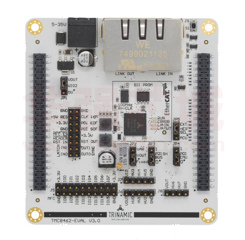
TMC8462-EVAL
Evaluation Board for TMC8462-BA, compatible with the modular Landungsbruecke system, RJ45 twisted pair copper interface
79mm x 85mm
Landungsbruecke
MCU Board
85mm x 55mm
TMC8462-BOB-ETH
Breakout Board (BOB) for TMC8462-BA, with 0.1" header rows,
reference clock source, SII-EEPROM, and RJ45 twisted pair copper transceiver interface
2.0" x 1.5"
Table 1: TMC8462 order codes
Trademark and Patents
EtherCAT® is a registered trademark and patented technology, licensed by Beckhoff Automation GmbH,
Germany.
©2019 TRINAMIC Motion Control GmbH & Co. KG, Hamburg, Germany
Terms of delivery and rights to technical change reserved.
Download newest version at www.trinamic.com
�TMC8462 Datasheet • Document Revision V1.5 • 2019-June-21
3
7 / 204
Principles of Operation / Key Concepts
TMC8462 is a highly integrated ASIC providing the interface between the Ethernet-based EtherCAT real-time
field bus and the local application. Its extended digital and high voltage feature set provides additional
functions to the EtherCAT slave.
3.1
General Device Architecture
Figure 1 shows the general device architecture and major connections of TMC8462. The four function
blocks EtherCAT Slave Controller, Multi-Function Control and IO, Analog and High Voltage, and Ethernet
PHYs are introduced in the following sub-sections.
For operation, a stable 100MHz clock source, an IIC EEPROM, and power supply for IO and high voltage
operation are required (if the high voltage features are used). An application controller, which also runs
the EtherCAT slave stack, connects to the SPI interfaces. The application and onboard peripherals can be
controlled by the application controller or the Multi-Function Control and IO block.
Figure 1: General device architecture
©2019 TRINAMIC Motion Control GmbH & Co. KG, Hamburg, Germany
Terms of delivery and rights to technical change reserved.
Download newest version at www.trinamic.com
�TMC8462 Datasheet • Document Revision V1.5 • 2019-June-21
3.2
8 / 204
EtherCAT Slave Controller
TMC8462 contains a standard-conform EtherCAT Slave Controller (ESC) providing real-time EtherCAT MAC
layer functionality to EtherCAT slaves. It connects via MII interface to standard Ethernet PHYs and provides
a digital control interface to a local application controller while also providing the option for standalone
operation.
The ESC part of TMC8462 provides the following EtherCAT-related features. More information is available
in Section 6.
• Two internal 100Mbit Ethernet PHYs
• Eight Fieldbus Memory Management Units (FMMU)
• Eight Sync Managers (SM)
• 16 KByte of Process Data RAM (PDRAM)
• 64B bit Distributed Clocks support
• I2C interface for external EEPROM for ESC configuration
• SPI Process Data Interface (PDI) with 30Mbit/s
• Proven EtherCAT State Machine (ESM)
• Device Emulation Mode
3.3
Multi-Function and Control IO Block
In addition to the EtherCAT functionality, the TMC8462 comes with a dedicated function block providing a
configurable set of complex real-time IO functionality for smart (embedded) EtherCAT slave systems. This
IO functionality is called Multi-Function Control and IO block (MFC IO). Its special focus is on motor and
motion control while it is not limited to this application area.
The MFC IO block combines various functional sub blocks that are helpful in an embedded design to
reduce complexity, to simplify bill of materials (BOM), and to provide hardware acceleration to compute
intensive or time critical tasks. More information is available in Section 7.
Configurable IO Ports The whole MFC IO block provides in total 24 IO ports that can be configured and
assigned to any of the available functional units inside the MFC IO block. If not used, each IO port can be
tristated.
General Purpose IOs Up to sixteen (16) general purpose IOs are available. Each IO can be configured
either as input or as output. For the outputs, a safe state can be configured which is used in case of
emergency event.
Incremental Encoder Interface Configurable incremental encoder interface with 32 bit position registers, single-ended or differential inputs, configurable counting constant for different resolutions, configurable polarity and N-signal behavior.
Step/Direction Generator Block The step and direction unit provides upt to 3 independent channels.
Various configuration options and modes allow for example for continuous or one-shot mode, reading of
the internal total step counters, pre-loading the next step frequency to be used at a certain counter value.
The step and direction outputs signals can be single-ended or differential.
©2019 TRINAMIC Motion Control GmbH & Co. KG, Hamburg, Germany
Terms of delivery and rights to technical change reserved.
Download newest version at www.trinamic.com
�TMC8462 Datasheet • Document Revision V1.5 • 2019-June-21
9 / 204
PWM Block The integrated PWM block provides up to 4 PWM channels. PWM frequency and duty cycle
as well as polarities and dead times are configurable. The outputs can be configured for a safe state in
case of emergency.
Generic SPI Master Interface The TMC8462 provides a generic SPI master interface to connect to onor off-board SPI slave peripherals like ADCs, sensors, or motor drivers. The SPI master interface is fully
configurable and offers 4 slave select lines.
Generic I2C Master Interface A generic I2C master interface is also available in TMC8462 to connect to
I2C slaves. The I2C bus speed is configurable.
Digital DAC A simple digital 16 bit DAC channel is available which requires an external RC circuit for
operation.
Safety Functions
The following safety functions are available with the TMC8462
• Configurable watchdog functionality for the MFC IO block to monitor internal and external signals as
well as EtherCAT activity. This block is fully configurable.
• A general emergency switch input can be activated. For critical outputs, a safe state can be configured
which is used when the emergency switch triggers.
• A common IRQ signal is available at the MFC IO block which can be mapped to various events of the
MFC IO block. The IRQ events can be processed by a local application controller.
3.4
Analog and High Voltage Block
TMC8462 has an integrated powerful high voltage sub block that provides analog functions and high
voltage support to your EtherCAT slave. The integrated high voltage capabilities allow for BOM reduction
and save board space. More information is available in Section 7.21.
High Voltage Ports 8 of the 24 configurable IO ports of the MFC IO block are high voltage IO ports. For
pure digital systems operating at 3.3V or 5V these ports can simply be used as standard IO ports. When
using a higher supply voltage at the VIOx inputs the high voltage ports can be used at up to 35V (5V, 12V,
24V typical). The 8 high voltage ports are grouped into 3 groups with 2, 3, and 3 ports. Each group can be
used a different supply voltage level using VIO1, VIO2, and VIO3 inputs.
Each high voltage port has a short circuit protected push-/pull or open drain output stage with 100mA
drive current (ca. 200mA short time) and can be combined with any signal of the MFC IO block functions.
The outputs’ slope can be controlled. An optional input filter is selectable as well as pull downs or pull ups
with 100µA.
The high voltage ports have an over-temperature shutdown.
WARNING
When driving inductive loads a freewheeling diode must be provided to the high
voltage I/O pins to prevent from latch-up.
Switching Regulators Two switching regulators (buck regulators) are integrated into TMC8462 – SW0
and SW1. Both are capable of driving up to 500mA.
SW0 generates a fixed 3.3V rail for internal and external logic supply. SW1 is programmable between 3.3V
and VS (up to 24V) and can be used for peripheral supply, e.g, to generate a 5V encoder supply.
Each switching regulator comes with a separate over-temperature shutdown.
©2019 TRINAMIC Motion Control GmbH & Co. KG, Hamburg, Germany
Terms of delivery and rights to technical change reserved.
Download newest version at www.trinamic.com
�TMC8462 Datasheet • Document Revision V1.5 • 2019-June-21
10 / 204
Single Supply Operation TMC8462 is designed to work with a single external power supply rail. All
required supply voltages are generated internally. The required external supply rail depends on the
application scenario (between 3.3V and 24V).
3.5 Interfaces
Field Bus Interface TMC8462 contains 2 integrated 100-Mbit Ethernet PHYs and directly connects to the
field bus using an external transformer circuit. In addition, the PHY interfaces of two TMC8462 devices can
also be connected directly to allow back-to-back connection with only low part count and a small circuit.
This is useful when extending the EtherCAT bus on the board or to a another slave close by.
ESC Process Data Interface The ESC part can be accessed via the so-called Process Data Interface (PDI).
TMC8462 comes with an SPI PDI. Besides the standard SPI bus lines additional control signals belong to
the SPI PDI, which are further described in Section 5.1..
MFC IO Control Interface The MFC IO block of TMC8462 can be accessed from EtherCAT master side
or from the local application controller. For connection to the local application controller, a second SPI
interface – the MFC IO SPI – is provided. The protocol used nearly identical to the SPI PDI interface.
Additional information on the MFC IO SPI is given in Section 5.2.
EEPROM Interface The EEPROM interface is intended to be a point-to-point interface between TMC8462
and EEPROM with TMC8462 being the master. If other I2C masters are required to access the I2C bus,
TMC8462 must be held in reset state, for example for in-circuit-programming of the EEPROM. During
operation, the application controller must tristate its I2C interface. Depending on the EEPROM size the
addressing mode must be properly set using the PROM_SIZE configuration pin.
Configuration Inputs Hard-wired configuration pins are available at the TMC8462, which are used to
configure various options related to the hardware configuration and application scenario and which will
not change. These pins are PROM_SIZE, PDI_SHARED_SPI_BUS, and DEVICE_EMULATION.
More information on these configuration pins and signals is given in Section 4.2 and Section 5.
3.6
Software- and Tool-Support
TRINAMIC’s EtherCAT Slave Controller family comes with extensive hardware and software tool support to
get started quickly.
Evaluation Board An evaluation board is available for the TMC8462 with standard RJ45 connectors and
transformers for interfacing twisted pair copper (TPC) media.
©2019 TRINAMIC Motion Control GmbH & Co. KG, Hamburg, Germany
Terms of delivery and rights to technical change reserved.
Download newest version at www.trinamic.com
�TMC8462 Datasheet • Document Revision V1.5 • 2019-June-21
11 / 204
Figure 2: TMC8462 Evaluation Board
The complete board design files are available for download and can be used as reference. All information
is available for download on the specific product page on TRINAMIC’s website at
http://www.trinamic.com/products/integrated-circuits/evalboards.
Breakout Board (BOB) Besides the Evaluation board another smaller breakout board is available. It
allows for easy integration into own systems or connection to a prototyping platform. The breakout
board provides the bus interface along with the ESC and requires an appropriate supply and controller
connection. The BOB comes with standard RJ45 connectors to connect to TPC using the TMC8462 ESC
with integrated Ethernet PHYs. TMC8462 is functionally equal to the TMC8461. The difference is in using
external PHYs vs. integrated PHYs. The complete board design files are available for download and can
be used as reference. All information is available for download from the evaluation board section on
TRINAMIC’s website at
https://www.trinamic.com/support/eval-kits/.
©2019 TRINAMIC Motion Control GmbH & Co. KG, Hamburg, Germany
Terms of delivery and rights to technical change reserved.
Download newest version at www.trinamic.com
�TMC8462 Datasheet • Document Revision V1.5 • 2019-June-21
12 / 204
Figure 3: TMC8462 breakout board for RJ45 and TPC
TRINAMIC Technology Access Package In addition, a comprehensive source code and software package
– TRINAMIC Technology Access Package (TTAP) – is available for download to get started quickly with own
code.
The TTAP is available at https://www.trinamic.com/support/software/access-package/.
TMCL-IDE The TMCL-IDE is TRINAMIC’s primary tool (for Windows PCs) to control TRINAMIC modules and
evaluation boards. Besides, it provides feature like remote firmware updates, module monitoring options,
and specific Wizard support. The TMCL-IDE can be used along with TRINAMICs modular evaluation board
system.
Figure 4: TMCL-IDE
©2019 TRINAMIC Motion Control GmbH & Co. KG, Hamburg, Germany
Terms of delivery and rights to technical change reserved.
Download newest version at www.trinamic.com
�TMC8462 Datasheet • Document Revision V1.5 • 2019-June-21
13 / 204
The latest version and additional information is available for download from TRINAMIC’s website at
http://www.trinamic.com/software-tools/tmcl-ide.
EtherCAT Slave Configuration Configuration of the EtherCAT Slave Controller is done during boot time
with configuration information read from the SII EEPROM after reset or power cycling. This information
must be (pre)programmed into the SII EEPROM. This can be done via the EtherCAT master using a so-called
EtherCAT Slave Information (ESI) file in standardized XML format. The SII EEPROM can also be (re)written
using the local application controller.
ESI Configuration Wizard The TMCL-IDE contains a wizard to assist users with the configuration of the
TMC8462 various MFC IO functions. The wizard shows available and allowed options and provides XML
code snippets for the ESI file for the SII EEPROM as well as generic C-Code blocks. These can be used as
starting point for own firmware development for the application controller.
Figure 5: Configuration wizard example – MFC IO block configuration
©2019 TRINAMIC Motion Control GmbH & Co. KG, Hamburg, Germany
Terms of delivery and rights to technical change reserved.
Download newest version at www.trinamic.com
�TMC8462 Datasheet • Document Revision V1.5 • 2019-June-21
Figure 6: Configuration wizard example – SII EEPROM content and C-code output
©2019 TRINAMIC Motion Control GmbH & Co. KG, Hamburg, Germany
Terms of delivery and rights to technical change reserved.
Download newest version at www.trinamic.com
14 / 204
�15 / 204
TMC8462 Datasheet • Document Revision V1.5 • 2019-June-21
4
4.1
Device Pin Definitions
Pinout and Pin Coordinates of TMC8462-BA
1
3
2
4
5
6
7
8
9
10
11
A
B
C
D
E
F
G
H
J
K
L
Figure 7: TMC8462-BA Pinout top view
4.2
Signal Descriptions
Name
Pin
Type (I,O,PU,PD)
Function
NRESET
K4
I/O
Low active system reset. NRESET is an I/O pin.
Connected to VCCIO via a 10K resistor and to
GND via a 10nF capacitor if no other reset source
for proper power-on reset is used. For more
information see Section 5.4.1.
REF_CLK100_IN
L3
I
100MHz Reference clock input, connect to a clock
source 16kBit is used (an additional address byte is required then). 0 = up to
16kBit EEPROM, 1 = 32 kBit-4Mbit EEPROM
EEPROM IOs
DC Synchronization IOs
SYNC_OUT0
D7
O
Distributed Clocks synchronization output 0, typically connect to MCU
SYNC_OUT1
D6
O
Distributed Clocks synchronization output 1, typically connect to MCU
LATCH_IN0
C7
I
Latch input 0 for Distributed Clocks, connect to
GND if not used.
LATCH_IN1
C6
I
Latch input 1 for Distributed Clocks, connect to
GND if not used.
LED_RUN
B3
O
Run Status LED, connect to green LED (Anode) 0
= LED off, 1 = LED on
LED_ERR
C3
O
Error Status LED, connect to red LED (Anode) 0 =
LED off, 1 = LED on
LINK_ACT0
D3
O
Link In Port Status and Activity, connect to green
LED (Anode) 0 = LED off, 1 = LED on
LINK_ACT1
E3
O
Link Out Port Status and Activity, connect to
green LED (Anode) 0 = LED off, 1 = LED on
LEDs
©2019 TRINAMIC Motion Control GmbH & Co. KG, Hamburg, Germany
Terms of delivery and rights to technical change reserved.
Download newest version at www.trinamic.com
�18 / 204
TMC8462 Datasheet • Document Revision V1.5 • 2019-June-21
Name
Pin
Type (I,O,PU,PD)
Function
Process Data Interface IOs to/from MCU
PDI_SOF
H3
O
Ethernet Start-of-Frame if 1
PDI_EOF
G3
O
Ethernet End-of-Frame if 1
PDI_SPI_CSN
L4
I
Chip select signal of the process data interface
PDI_SPI_SCK
K3
I
Serial clock signal of the process data interface
PDI_SPI_MOSI
L5
I
Serial data out signal of the process data interface
PDI_SPI_MISO
K5
O
Serial data in signal of the process data interface
PDI_SPI_IRQ
J3
O
Interrupt signal for primary process data interface, connect to MCU
PDI_WDSTATE
G4
O
EtherCAT Watchdog state, 0: Expired, 1: Not expired
PDI_WDTRIGGER
F4
O
EtherCAT Watchdog trigger if 1
PDI_EMULATION
J7
I
Selects between PDI interface (SPI) or standalone
operation with state machine emulation inside
ESC. Has weak internal pull down. 0 = default,
PDI interface active, 1 = standalone operation,
state machine emulation in Slave Controller
MFC IO Control Interface IOs
MFC_CTRL_SPI_CSN
D4
I
Chip select signal of the MFC IO control interface
MFC_CTRL_SPI_SCK
E4
I
Serial clock signal of the MFC IO control interface
MFC_CTRL_SPI_MOSI
C4
I
Serial data out signal of the MFC IO control interface
MFC_CTRL_SPI_MISO
E7
O
Serial data in signal of the MFC IO control interface
MFC_IRQ
E6
O
MFCIO block IRQ for configurable events, connect
to MCU, high active
MFC_NES
C5
I
low active (not) Emergency Stop/Switch/Halt (to
bring PWM or other outputs into a safe state),
the event must be cleared actively, has weak internal pull down, must be driven high for normal
operation
PDI_SHARED_BUS
F9
I
Selects between separate SPI buses (MISO, MOSI,
SCK) or one SPI bus with two CS lines for the PDI
and MFC CTRL SPI interface: 0 = two separate SPI
buses, 1 = one shared SPI bus using the PDI_SPI_x
bus lines
©2019 TRINAMIC Motion Control GmbH & Co. KG, Hamburg, Germany
Terms of delivery and rights to technical change reserved.
Download newest version at www.trinamic.com
�19 / 204
TMC8462 Datasheet • Document Revision V1.5 • 2019-June-21
Name
Pin
Type (I,O,PU,PD)
Function
MFCIO00
J8
I/O
MFCIO block low voltage I/O
MFCIO01
J9
I/O
MFCIO block low voltage I/O
MFCIO02
J10
I/O
MFCIO block low voltage I/O
MFCIO03
J11
I/O
MFCIO block low voltage I/O
MFCIO04
H8
I/O
MFCIO block low voltage I/O
MFCIO05
H9
I/O
MFCIO block low voltage I/O
MFCIO06
H10
I/O
MFCIO block low voltage I/O
MFCIO07
H11
I/O
MFCIO block low voltage I/O
MFCIO08
D8
I/O
MFCIO block low voltage I/O
MFCIO09
D9
I/O
MFCIO block low voltage I/O
MFCIO10
D10
I/O
MFCIO block low voltage I/O
MFCIO11
D11
I/O
MFCIO block low voltage I/O
MFCIO12
C8
I/O
MFCIO block low voltage I/O
MFCIO13
C9
I/O
MFCIO block low voltage I/O
MFCIO14
C10
I/O
MFCIO block low voltage I/O
MFCIO15
C11
I/O
MFCIO block low voltage I/O
MFC_HV0 (MFCIO16)
A4
I/O
MFCIO block high voltage I/O
MFC_HV1 (MFCIO17)
A5
I/O
MFCIO block high voltage I/O
MFC_HV2 (MFCIO18)
A6
I/O
MFCIO block high voltage I/O
MFC_HV3 (MFCIO19)
A7
I/O
MFCIO block high voltage I/O
MFC_HV4 (MFCIO20)
A8
I/O
MFCIO block high voltage I/O
MFC_HV5 (MFCIO21)
A9
I/O
MFCIO block high voltage I/O
MFC_HV6 (MFCIO22)
A10
I/O
MFCIO block high voltage I/O
MFC_HV7 (MFCIO23)
A11
I/O
MFCIO block high voltage I/O
MFC IOs
MFC High Voltage IOs
©2019 TRINAMIC Motion Control GmbH & Co. KG, Hamburg, Germany
Terms of delivery and rights to technical change reserved.
Download newest version at www.trinamic.com
�20 / 204
TMC8462 Datasheet • Document Revision V1.5 • 2019-June-21
Name
Pin
Type (I,O,PU,PD)
Function
MFC High Voltage IO Supplies
VIO1
B5
I
MFCHVIO block 1 supply voltage
VIO2
B7
I
MFCHVIO block 2 supply voltage
VIO3
B9
I
MFCHVIO block 3 supply voltage
GNDIO1
B6
I
MFCHVIO block 1 ground, connect to GND
GNDIO2
B8
I
MFCHVIO block 2 ground, connect to GND
GNDIO3
B10
I
MFCHVIO block 3 ground, connect to GND
Device Supply and Ground
VS
B11
I
Supply voltage, use a 100nF filter capacitor
VCCIO
E10, F10,
I
I/O supply voltage, use a 100nF filter capacitor
per pin
I
Core supply voltage, connect to VDD1V8_OUT,
use a 100nF filter capacitor per pin
G10, F11
VCC_CORE
F6, G6,
F7, G7
PLLCLK_VCCIO
K6
I
PLL supply voltage, connect to VCCIO through
a filter (R/L/C)
TSTCLK_SELECT
H6
I
Test input, always connect to VCCIO for normal operation
GND
C1, F1,
I
Supply Ground
J6
I
PLL supply ground, connect to GND
VDD1V8_OUT
G11
O
Output of internal 1.8V regulator, use a 100nF
filter capacitor
VDD5_OUT
E11
O
Output of internal 5V regulator, use a 100nF filter capacitor if VS≥5V
J1, A3,
B4, F5,
G5, E8,
F8, G8
PLLCLK_GND
Voltage Regulator IOs
©2019 TRINAMIC Motion Control GmbH & Co. KG, Hamburg, Germany
Terms of delivery and rights to technical change reserved.
Download newest version at www.trinamic.com
�21 / 204
TMC8462 Datasheet • Document Revision V1.5 • 2019-June-21
Name
Pin
Type (I,O,PU,PD)
Function
Switching Regulator 0 IOs
VS0
L7
I
Switching regulator 0 supply voltage, Switching
regulator 0 provides a fixed 3.3V output.
GND0
L9
I
Switching regulator 0 ground, connect to GND
SW0
L8
O
Switching regulator 0 output, fixed 3.3V
SW_DIODE
K7
I
Switching regulator 0 internal diode, connect to
SW0 only if VS0 is at or below 5V
GND_DIODE
K8
I
Switching regulator 0 internal diode ground, connect to GND
Switching Regulator 1 IOs
VS1
L11
I
Switching regulator 1 supply voltage, Switching
regulator 1 provides an adjustable output voltage.
GND1
K9
I
Switching regulator 1 ground, connect to GND
SW1
L10
O
Switching regulator 1 output, adjustable
VOUT
K10
I
Switching regulator 1 inductor ringing suppression feedback
VOUT_FB
K11
I
Switching regulator 1 feedback voltage, 1.2V typically
Bus Interface 0 IOs (EtherCAT IN Port)
TN0
D1
O
Negative pin of differential transmit output pair
TP0
E1
O
Positive pin of differential transmit output pair
RN0
A1
I
Negative pin of differential receive output pair
RP0
B1
I
Positive pin of differential receive output pair
REGOUT0
A2
O
Regulator power output, use a 10uF and 0.1uF
for filtering power noise
MCLK
F2
O
PHY management clock, leave open if not needed
MDIO
F3
I/O, PU
PHY management data, use 4K7 pull up resistor
to VCCIO (3.3V)
©2019 TRINAMIC Motion Control GmbH & Co. KG, Hamburg, Germany
Terms of delivery and rights to technical change reserved.
Download newest version at www.trinamic.com
�22 / 204
TMC8462 Datasheet • Document Revision V1.5 • 2019-June-21
Name
Pin
Type (I,O,PU,PD)
Function
Bus Interface 1 IOs (EtherCAT OUT Port)
TN1
K1
IO
Negative pin of differential transmit output pair
TP1
L1
IO
Positive pin of differential transmit output pair
RN1
G1
IO
Negative pin of differential receive output pair
RP1
H1
IO
Positive pin of differential receive output pair
REGOUT1
L2
O
Regulator power output, use a 10uF and 0.1uF
for filtering power noise
TST_MODE
E5
I
Test mode enable, connect to GND
TST_ANA
D5
O
Analog test output, leave open
RXCLK0
D2
IO
Clock test pin, leave open
RXCLK1
G2
IO
Clock test pin, leave open
TXCLK0
E2
IO
Clock test pin, leave open
TXCLK1
H2
IO
Clock test pin, leave open
RXDV0
B2
I, PD
Test pin, leave open for normal operation
RXDV1
K2
I, PD
Test pin, leave open for normal operation
TXER0
C2
I, PD
Test pin, leave open for normal operation
TXER1
J2
I, PD
Test pin, leave open for normal operation
CLKO_100
L6
O
100MHz clock output
Test Pins only
Table 2: Pin and Signal description for TMC8462-BA
©2019 TRINAMIC Motion Control GmbH & Co. KG, Hamburg, Germany
Terms of delivery and rights to technical change reserved.
Download newest version at www.trinamic.com
�23 / 204
TMC8462 Datasheet • Document Revision V1.5 • 2019-June-21
5
5.1
Device Usage and Handling
Process Data Interface
The Process Data Interface (PDI) is an SPI interface with a clock frequency of up to 30 MHz. The ESC
registers and the process data RAM can be accessed from an external microcontroller using this interface.
The interface can be configured via the EEPROM, however it is recommended to use the default configuration (SPI mode 3 with low active chip select). For further details, see the ESC SPI slave configuration
registers in Section 6.
Additionally, some signals are available that can be evaluated by the application controller.
Figure 8: PDI control signals
TMC8462 pin
Description
Typical pin on a MCU
PDI_SPI_CSN
SPI chip select for the TMC8462 PDI
SSx
PDI_SPI_SCK
SPI master clock
SCK
PDI_SPI_MOSI
Master out slave in data
MOSI
PDI_SPI_MISO
Master in slave out data
MISO
PDI_SPI_IRQ
Configurable IRQ from PDI
General purpose Input
PDI_EMULATION
0: default mode for complex slaves, state
machine changes processed in microcontroller
firmware (SSC); 1: device emulation mode for,
e.g., simple slaves, state machine changes
directly handled in the ESC
General purpose Output
or connected to either
ground or 3.3V.
PDI_SOF
Indicates start of an Ethernet/EtherCAT frame
(MII_RXDV = ’1’)
General purpose Input
©2019 TRINAMIC Motion Control GmbH & Co. KG, Hamburg, Germany
Terms of delivery and rights to technical change reserved.
Download newest version at www.trinamic.com
�24 / 204
TMC8462 Datasheet • Document Revision V1.5 • 2019-June-21
TMC8462 pin
Description
Typical pin on a MCU
PDI_EOF
Indicates end of an Ethernet/EtherCAT frame
General purpose Input
PDI_WDSTATE
0: Watchdog expired; 1: Watchdog not expired
General purpose Input
PDI_WDTRIGGER
Watchdog triggered if ’1’
General purpose Input
Table 3: PDI signal description
5.1.1
SPI protocol description
Each SPI datagram contains a 2- or 3-byte address/command part and a data part. For addresses below
0x2000, the 2-byte addressing mode can be used, the 3 byte addressing mode can be used for all addresses.
C2
C1
C0
Command
0
0
0
NOP (no operation, no following data bytes)
0
0
1
Reserved
0
1
0
Read
0
1
1
Read with wait state byte
1
0
0
Write
1
0
1
Reserved
1
1
0
Address extension, signaling 3 byte mode
1
1
1
Reserved
Table 4: PDI SPI commands
Address
A12 A11 A10 A9
A8
A7
A6
A5
A12 A11 A10 A9
A8
A7
A6
A5
Command
A4
A3
A2
A1
A0
A4
A3
A2
A1
Byte 0
Byte 1
Figure 9: PDI SPI 2 byte addressing
©2019 TRINAMIC Motion Control GmbH & Co. KG, Hamburg, Germany
Terms of delivery and rights to technical change reserved.
Download newest version at www.trinamic.com
A0
C2
C1
C0
C2
C1
C0
�25 / 204
TMC8462 Datasheet • Document Revision V1.5 • 2019-June-21
Address
A15 A14 A13 A12 A11 A10 A9
A12 A11 A10 A9
A8
A7
A6
A5
A4
Byte 0
Command
A8
A7
A6
A5
A4
A3
A2
A3
A2
A1
A0
1
1
0
Byte 1
A1
Address
extension
command
A0
C2
C1
C0
A15 A14 A13
C2
C1
Byte 2
C0
0
0
Reserved
Figure 10: PDI SPI 3 byte addressing
Unless highest performance is required, using only the 3-byte addressing mode and the read with wait
state command is recommended since it reduces the need for special cases in the software. During the
address/command bytes, the ESC replies with the contents of the event request registers (0x0220, 0x0221
and in 3 byte addressing mode 0x0222).
Command 0 - NOP
This command can be used for checking the event request registers and resetting the PDI watchdog
without a read or write access.
Example datagram:
Example reply (AL Control event bit is set):
0x00 0x00
0x01 0x00
Command 2 - READ
With the read command, an arbitrary amount of data can be read from the device. The first byte read is
the data from the address given by the address/command bytes. With every read byte, the address is
incremented. During the data transfer, the SPI master sends 0x00 except for the last byte where a 0xFF is
sent.
When using this command, a pause of 240ns or more must be included between the address/command
bytes and the data bytes for the ESC to fetch the requested data.
Example datagram (Read from address 0x0120 and 0x0121): 0x09 0x02 0x00 0xFF
Example reply (Operational State requested):
0x01 0x00 0x08 0x00
Command 3 - READ WITH WAIT STATE BYTE
This command is similar to the Read command with an added dummy byte between the address/command
part and the data part of the datagram. This allows enough time to fetch the data in any case.
Example datagram (Read starting at address 0x3400): 0xA0 0x06 0x2C 0xFF 0x00 0x00 0x00 0xFF
Example reply (0xXX is undefined data):
0x00 0x00 0x00 0xXX 0x44 0x41 0x54 0x41
Command 4 - WRITE
The write command allows writing of an arbitrary number of bytes to writable ESC registers or the process
data RAM. It requires no wait state byte or delay after the address/command bytes. After every transmitted
byte, the address is incremented.
Example datagram (Write starting at address 0x4200): 0x10 0x06 0x50 0x4C 0x48
Example reply (0xXX is undefined data):
0x00 0x00 0x00 0xXX 0xXX
Address 0x4200 now contains 0x4C, Address 0x4201 contains 0x48
©2019 TRINAMIC Motion Control GmbH & Co. KG, Hamburg, Germany
Terms of delivery and rights to technical change reserved.
Download newest version at www.trinamic.com
�26 / 204
TMC8462 Datasheet • Document Revision V1.5 • 2019-June-21
Command 6 - ADDRESS EXTENSION
The address extension command is mainly used for the 3-byte addressing mode as shown in Figure 10.
For SPI masters that can only process datagrams with an even number of bytes, it might be necessary to
pad the datagram to an even number of bytes. This can be achieved by duplicating the third byte of the
3-byte address/command part and using the address extension command in all but the last duplicate.
For example, a SPI master that is only capable of transmitting a multiple of 4 bytes cannot use the example
datagram for a write access above since it contains 5 bytes. With three added padding bytes, the master
has to transmit two 4-byte groups.
Example datagram (Write starting at address 0x4200):
Example reply (0xXX is undefined data):
5.1.2
0x10 0x06 0x58 0x58 0x58 0x50 0x4C 0x48
0x00 0x00 0x00 0xXX 0xXX 0xXX 0xXX 0xXX
Timing example
This example shows a generic read access with wait state and 2 byte addressing. All configurable options
are shown. The delays between the transferred bytes are just to show the byte boundaries and are not
required.
CSN active low
CSN acti ve high
SCK mode 0
SCK mode 1
SCK mode 2
SCK mode 3
A
12
MOSI
MISO mode 0/2
normal sample
I
7
MISO mode 0/2
late sample
MISO mode 1/3
normal sample
MISO mode 1/3
late sample
I
7
S
A
10
A
9
A
8
A
7
A
6
A
5
A
4
A
3
A
2
A
1
A
0
C
2
C
1
C
0
I
6
I
5
I
4
I
3
I
2
I
1
I
0
I
15
I
14
I
13
I
12
I
11
I
10
I
9
I
8
I
7
S
S
A
11
I
6
I
6
I
7
I
5
I
4
I
5
I
6
I
4
I
5
I
3
I
3
I
4
I
2
I
1
I
2
I
3
I
1
I
2
I
0
I
0
I
1
I
15
I
15
I
0
I
14
I
14
I
15
I
13
I
13
I
14
I
12
I
12
I
13
I
11
I
11
I
12
I
10
I
10
I
11
I
9
I
9
I
10
D
7
I
8
I
8
I
9
D
6
D
7
D
7
I
8
D
5
D
6
D
6
D
7
D
5
D
5
D
6
Figure 11: SPI timing example
©2019 TRINAMIC Motion Control GmbH & Co. KG, Hamburg, Germany
Terms of delivery and rights to technical change reserved.
Download newest version at www.trinamic.com
D
4
D
3
D
4
D
4
D
5
D
2
D
3
D
3
D
4
D
1
D
2
D
2
D
3
D
0
D
1
D
1
D
2
D
15
D
0
D
0
D
1
D
14
D
15
D
15
D
0
D
13
D
14
D
14
D
15
D
12
D
13
D
13
D
14
D
11
D
12
D
12
D
13
D
10
D
11
D
11
D
12
D
9
D
10
D
10
D
11
D
8
D
9
D
9
D
10
D
8
D
8
D
9
D
8
�27 / 204
TMC8462 Datasheet • Document Revision V1.5 • 2019-June-21
5.2
MFC IO Control Interface
The MFC IO block of the TMC8462 comes with a dedicated SPI slave interface to allow direct access from
a local application controller. It is called MFC CTRL SPI interface. This interface to the MFC IO block’s
functions is always available, even if the EtherCAT state machine is currently not in operational state (OP).
Protocol structure and timing are identical to the PDI SPI.
The MFC Control SPI is a SPI mode 3 slave with low active chip select. The SPI clock frequency can be up to
30MHz. The following diagram shows all signals related to the MFC CTRL SPI interface.
Figure 12: MFC control signals
TMC8462 pin
Description
Typical pin on a MCU
MFC_CTRL_SPI_CSN
SPI chip select for the TMC8462 PDI
SSx
MFC_CTRL_SPI_SCK
SPI master clock
SCK
MFC_CTRL_SPI_MOSI
Master out slave in data
MOSI
MFC_CTRL_SPI_MISO
Master in slave out data
MISO
MFC_IRQ
Configurable IRQ from MFC IO block
General purpose Input
PDI_SHARED_BUS
0: separate SPI buses for PDI and MFC CTRL; 1:
shared/common SPI bus for PDI and MFC CTRL
with 2 CSN signals using the PDI SPI bus. The SPI
bus signals MFC_CTRL_SPI_SCK,
MFC_CTRL_SPI_MISO, MFC_CTRL_SPI_MOSI can
be left open in this case
General purpose Output
or connected to either
ground or 3.3V.
Table 5: MFC CTRL SPI signal description
5.2.1
SPI Protocol description
The protocol of the MFC CTRL SPI is the same as the PDI SPI interface (see section 5.1.1) The addresses for
register access are calculated using the register number and the byte number in each register. To calculate
the address, the register number is shifted left by 4 bits and the byte number is added as the 4 lowest bits.
Access using the 3 byte addressing mode is possible, and can be used when 2 byte mode is not implemented for the PDI SPI but since the highest bits of the address are always 0, accessing the MFC Control
SPI via 2 byte mode is sufficient.
©2019 TRINAMIC Motion Control GmbH & Co. KG, Hamburg, Germany
Terms of delivery and rights to technical change reserved.
Download newest version at www.trinamic.com
�TMC8462 Datasheet • Document Revision V1.5 • 2019-June-21
28 / 204
6
6
Figure 13: MFC CTRL SPI 2 byte addressing
6
6
Figure 14: MFC CTRL SPI 3 byte addressing
5.2.2
Timing example
This example shows a generic MFC register read access with wait state. The delays between the transferred
bytes are just to show the byte boundaries and are not required.
Figure 15: MFC SPI timing example
5.2.3
Sharing Bus Lines with the PDI SPI
To reduce the number of signals on the PCB or if the local application controller has only one SPI interface,
the MFC CTRL SPI bus can share the SPI bus signals of the PDI SPI, requiring only separate chip select
signals. In this case, both interfaces are internally switched to the PDI SPI interface pins. The original MFC
CTRL SPI signals (MOSI, MISO, and SCK) remain unconnected in this case. Only the MFC_CTRL_SPI_CSN
pin/signal must be used if the MFCIO block is accessed.
©2019 TRINAMIC Motion Control GmbH & Co. KG, Hamburg, Germany
Terms of delivery and rights to technical change reserved.
Download newest version at www.trinamic.com
�TMC8462 Datasheet • Document Revision V1.5 • 2019-June-21
29 / 204
To share the SPI bus lines, configuration pin PDI_SHARED_BUS must be pulled high as shown in the figure
below.
Figure 16: SPI bus sharing
©2019 TRINAMIC Motion Control GmbH & Co. KG, Hamburg, Germany
Terms of delivery and rights to technical change reserved.
Download newest version at www.trinamic.com
�TMC8462 Datasheet • Document Revision V1.5 • 2019-June-21
5.3
30 / 204
Ethernet Physical Layer Connection
TMC8462 comes with two integrated 100-Mbit Ethernet PHYs eliminating the need for external PHY
components. The physical media interface can connect to (shielded) twisted pair copper buses ((S)TPC).
Port signals with index 0 represent the EtherCAT IN port. Port signals with index 1 represent the EtherCAT
OUT port.
Figure 17: Physical bus interface pins
TMC8462 pin
Description
TNx
Negative pin of differential transmit output pair
TPx
Positive pin of differential transmit output pair
RNx
Negative pin of differential receive output pair
RPx
Positive pin of differential receive output pair
REGOUTx
This is a regulator power output. A 10uF and 0.1uF should be connected to
this pin for filtering power noise.
MCLK
PHY configuration clock output
MDIO
PHY configuration data in-/output
Table 6: Physical bus interface pin description
©2019 TRINAMIC Motion Control GmbH & Co. KG, Hamburg, Germany
Terms of delivery and rights to technical change reserved.
Download newest version at www.trinamic.com
�31 / 204
TMC8462 Datasheet • Document Revision V1.5 • 2019-June-21
5.4
5.4.1
External Circuitry and Applications Examples
Device Reset
The NRESET signal should at least be connected to VCCIO via a 10K resistor and to GND via a 10nF capacitor
if no other controlled reset source for proper power-on behavior and reset is used.
VCCIO (3.3V)
TMC8462
10kΩ
NRESET
10nF
Figure 18: Minimum external circuit for power-on reset
5.4.2
Supply Filtering for PLL Supply
The internal PLL is supplied with the same 3.3V as used for VCCIO. An R/L/C filter structure as shown in the
circuit diagram is used. PLLCLK_GND is connected to common ground.
VCCIO (3.3V)
VCCIO (3.3V)
TMC8462
TSTCLK_SELECT
1Ω
600 Ω @100MHz
PLLCLK_VCCIO
100nF
PLLCLK_GND
Figure 19: PLL supply filter
©2019 TRINAMIC Motion Control GmbH & Co. KG, Hamburg, Germany
Terms of delivery and rights to technical change reserved.
Download newest version at www.trinamic.com
�32 / 204
TMC8462 Datasheet • Document Revision V1.5 • 2019-June-21
5.4.3
PHY Power Regulator Filtering
The internal PHY circuits require external filter capacitors.
TMC8462
REGOUT0
10µF
100nF
REGOUT1
10µF
100nF
Figure 20: PHY power regulator filtering
©2019 TRINAMIC Motion Control GmbH & Co. KG, Hamburg, Germany
Terms of delivery and rights to technical change reserved.
Download newest version at www.trinamic.com
�33 / 204
TMC8462 Datasheet • Document Revision V1.5 • 2019-June-21
5.4.4
External Circuit for Fixed Switching Regulator 0
Switching regulator 0 is an internal buck switching regulator and generates a fixed 3.3V supply with approximately 500mA. This 3.3V supply shall be used to power VCCIO and PLLCLK_VCCIO. This regulator comes
with an integrated Schottky diode which minimizes part count, when an external 5V supply is available.
This 3.3V can also be used to power other on-board devices, e.g., EEPROM or LEDs. The 3.3V rail is available
at switching regulator 0 output SW0.
More information on the switching regulators is given in Section 7.21.
TMC8462
VS=5V
VS0
22µH
SW0
3.3V out
SW_DIODE
+
22µF
GND_DIODE
47µF
GND0
Figure 21: External circuit for switching regulator 0 with VS0 = 5V
TMC8462
VS0
VS>5V
22µH
SW_DIODE
GND0
22µF
+
GND_DIODE
3.3V out
MSS1P6
SW0
47µF
Figure 22: External circuit for switching regulator 0 with VS0 > 5V
©2019 TRINAMIC Motion Control GmbH & Co. KG, Hamburg, Germany
Terms of delivery and rights to technical change reserved.
Download newest version at www.trinamic.com
�34 / 204
TMC8462 Datasheet • Document Revision V1.5 • 2019-June-21
5.4.5
External Circuit for Adjustable Switching Regulator 1
Switching regulator 1 is an internal buck switching regulator and generates an adjustable supply rail with
approximately 500mA. The voltage at SW1 can be adjusted using a resistor network in the switching
regulator’s feedback path at VOUT_FB. VOUT_FB should be at 1.2V using a resistor divider. SW1 can be
used to power the high voltage IOs using VIO1, VIO2, VIO3 as well as switching regulator 0 input VS0 (which
generates a fixed 3.3V rail). SW1 can also be used to power other peripheral devices, e.g., Hall signals of a
BLDC motor or external encoders.
More information on the switching regulators is given in Section 7.21.
TMC8462
VS1
VS
22µH
adj. out
22µF
+
MSS1P6
SW1
100kΩ
47µF
VOUT
4.7kΩ
VOUT_FB
GND1
Figure 23: External circuit for adjustable buck regulator
©2019 TRINAMIC Motion Control GmbH & Co. KG, Hamburg, Germany
Terms of delivery and rights to technical change reserved.
Download newest version at www.trinamic.com
�35 / 204
TMC8462 Datasheet • Document Revision V1.5 • 2019-June-21
5.4.6
Minimum External Supply Circuit for Single 3.3V Supply
The diagram shows the minimum external circuit when using a single 3.3V supply only.
Both internal switching regulators are not used in this example. Therefore, both supply ports VS0 and VS1
are not connected.
The high voltage IOs are also not used in this example. Therefore, the three high voltage IO supply ports
VIO1, VIO2, and VIO3 are not connected.
VS=3.3V
VS=3.3V
TMC8462 Supply
VS
VDD5_OUT
100nF
VS0
VS1
SW1
VOUT
4x VCCIO
VOUT_FB
4x100nF
GND1
1Ω
600 Ω @100MHz
PLLCLK_VCCIO
SW0
100nF
SW_DIODE
GND_DIODE
1.8V
GND0
VDD1V8_OUT
100nF
10x GND
4x VCC_CORE
PLLCLK_GND
4x100nF
VIO1/2/3
GNDIO1/2/3
Figure 24: Minimum external supply circuit for single 3.3V supply
©2019 TRINAMIC Motion Control GmbH & Co. KG, Hamburg, Germany
Terms of delivery and rights to technical change reserved.
Download newest version at www.trinamic.com
�36 / 204
TMC8462 Datasheet • Document Revision V1.5 • 2019-June-21
5.4.7
Minimum External Supply Circuit for Single 5V Supply
The diagram shows the minimum external circuit when using a single 5V supply only.
Switching regulator 0 is used to generate the 3.3V for VCCIO and PLLCLK_VCCIO.
Switching regulator 1 is not used in this example. Therefore, supply port VS1 is not connected.
The high voltage IOs are also not used in this example. Therefore, the three high voltage IO supply ports
VIO1, VIO2, and VIO3 are not connected.
VS=5V
TMC8462 Supply
VS
VDD5_OUT
100nF
100nF
SW1
VS0
100nF
VOUT
VOUT_FB
VS1
GND1
3.3V
3.3V
4x VCCIO
22µH
4x100nF
SW0
1Ω
SW_DIODE
PLLCLK_VCCIO
GND_DIODE
22µF
100nF
GND0
1.8V
VDD1V8_OUT
100nF
10x GND
4x VCC_CORE
PLLCLK_GND
4x100nF
VIO1/2/3
GNDIO1/2/3
Figure 25: Minimum external supply circuit for single 5V supply
©2019 TRINAMIC Motion Control GmbH & Co. KG, Hamburg, Germany
Terms of delivery and rights to technical change reserved.
Download newest version at www.trinamic.com
47µF
+
600 Ω @100MHz
�37 / 204
TMC8462 Datasheet • Document Revision V1.5 • 2019-June-21
5.4.8
Minimum External Supply Circuit for Single Supply >5V
To connect TMC8462 to a single supply greater than 5V the circuit is very similar to Figure 25. The main
difference is that an additional external diode (MSS1P6) is required at output SW0. The pin SW_DIODE is
open.
VS>5V
TMC8462 Supply
VS
VDD5_OUT
100nF
100nF
SW1
VS0
100nF
VOUT
VOUT_FB
VS1
3.3V
GND1
4x VCCIO
3.3V
4x100nF
22µH
SW0
1Ω
600 Ω @100MHz
1.8V
+
GND_DIODE
100nF
MSS1P6
SW_DIODE
PLLCLK_VCCIO
22µF
GND0
VDD1V8_OUT
100nF
10x GND
4x VCC_CORE
PLLCLK_GND
4x100nF
VIO1/2/3
GNDIO1/2/3
Figure 26: Minimum external supply circuit for single supply >5V
©2019 TRINAMIC Motion Control GmbH & Co. KG, Hamburg, Germany
Terms of delivery and rights to technical change reserved.
Download newest version at www.trinamic.com
47µF
�38 / 204
TMC8462 Datasheet • Document Revision V1.5 • 2019-June-21
5.4.9
Typical Power Supply Chain Using Both Buck Converters
VS
5V. . . 24V
VS, VS1, VIO1, VIO2, VIO3
Adj. buck converter
5V. . . 24V, 32kBit)
5.4.12
Considerations on PHY to PHY Connection
In applications with multiple EtherCAT slave controllers in one enclosed device or even on the same PCB, it
is not always necessary to connect the slave controllers via magnetics, RJ-45 connectors (or similar) and a
patch cable. Instead a direct backbone connection or traces on the PCB can be used to directly link the
PHYs, however coupling capacitors must be used in the connection.
This option reduces the cost as well as the required space in the setup.
Note
This connection method should be used only over short distances with no or few
connectors in between. It is not recommended for longer distances, especially
using a wired connection.
TMC8462 #1 OUT port
TMC8462 #2 IN port
TX+
TX+
TX-
TX-
RX+
RX+
RX-
RXall capacitors 33nF
Figure 30: Direct PHY to PHY connection
©2019 TRINAMIC Motion Control GmbH & Co. KG, Hamburg, Germany
Terms of delivery and rights to technical change reserved.
Download newest version at www.trinamic.com
�TMC8462 Datasheet • Document Revision V1.5 • 2019-June-21
6
40 / 204
EtherCAT Slave Controller Description
6.1
General EtherCAT Information
TMC8462 contains a standard-conform EtherCAT Slave Controller (ESC) providing real-time EtherCAT
MAC layer functionality to EtherCAT slave devices. The ESC part of TMC8462 provides the following
EtherCAT-related features:
• 16 KByte of Process Data RAM (PDRAM): The PDRAM is a dual ported RAM, which allows exchange of
data between the EtherCAT master and the local application.
• Eight Sync Managers (SM): Sync Managers are used to control and secure the data exchange via the
PDRAM in terms of data consistency, data security, and synchronized read/write operations on the
data objects. Two modes –buffered mode and mailbox mode – are available.
• Eight Fieldbus Memory Management Units (FMMU): FMMUs are used for mapping of logical addresses
to physical addresses. The EtherCAT master uses logical addressing for data than spans multiple
slaves. An FMMU can map such a logical address range to a continuous local physical address range.
• 64 bit Distributed Clock support (DC): DC is the base of the real-time capability of EtherCAT. Their
underlying algorithms compute delay times between the master and the slaves and between slaves
and update a common time stamp in all slaves. This way, synchronized time stamps (LATCH0/1) and
synchronized trigger signals (SYNC0/1) are available in every slave and to the master.
• IIC interface for external SII EEPROM for ESC configuration: After reset and at power up, the ESC
requires reading basic (and advanced) configuration data from an external SII EEPROM to properly
configure interfaces, operation modes, and and feature availability. The SII EEPROM may be read and
written by the master or the local application controller as well.
• SPI Process Data Interface (PDI): The PDI is the interface between the local application controller
and the ESC. Application-specific process data and EtherCAT control and status information for the
EtherCAT State Machine (ESM) is exchanged via this interface.
• Device Emulation Mode: This mode is a special mode of operation where no ESM in the application
controller is required. The slave’s operation states are simply directly set by the master without
control of an ESM. This is beneficial for small and simple slaves, for example simple IO devices.
To manufacture own slaves devices, a registration with the EtherCAT Technology Group (ETG) is required.
More information and resources on the EtherCAT technology and the EtherCAT standard are available
here:
• EtherCAT Technology Group (ETG) (http://www.ethercat.org/)
• EtherCAT is standardized by the IEC (http://www.iec.ch/) and filed as IEC-Standard 61158.
©2019 TRINAMIC Motion Control GmbH & Co. KG, Hamburg, Germany
Terms of delivery and rights to technical change reserved.
Download newest version at www.trinamic.com
�41 / 204
TMC8462 Datasheet • Document Revision V1.5 • 2019-June-21
6.2
Overview of Available Chip Features
Chip Feature / Description
Domain
TMC8460
TMC8461
TMC8462
TMC8670
The following table shows EtherCAT chip features available in TRINAMIC’s EtherCAT slave controller solutions.
Extended DL control register 0x0102:0x0103 enabled
Register
1
1
1
1
AL Status code register 0x0134:0x0135 enabled
Register
1
1
1
1
ECAT interrupt mask 0x0200:0x0201 enabled
Register
1
1
1
1
Configured station alias 0x0012:0x0013 enabled
Register
1
1
1
1
General purpose inputs 0x0F18:0x0F1F enabled
Register
0
0
0
0
General purpose outputs 0x0F10:0x0F17 enabled
Register
0
0
0
0
AL event mask 0x0204:0x0207 enabled
Register
1
1
1
1
Physical RD/WR offset 0x0108:0x0109 enabled
Register
0
1
1
0
Bridge port PDI (0x07) enabled
Register
0
0
0
0
Writable Watchdog divider 0x0400:0x0401 and Watchdog PDI
0x0410:0x0411 enabled
Watchdog
1
1
1
0
Watchdog counters 0x0442:0x0444 enabled
Watchdog
1
1
1
1
ECAT write protection 0x0020:0x0031 enabled
Ext. Function
0
1
1
0
Reset registers 0x0040:0x0041 enabled
Ext. Function
1
1
1
1
FPGA update at 0x0E00 enabled
Ext. Function
0
0
0
0
DC Sync event times enabled
Ext. Function
1
1
1
0
ECAT processing unit and PDI error counters/PDI error code
0x030C:0x030E enabled
Ext. Function
1
1
1
0
User RAM disabled
Ext. Functions
1
0
0
0
1: POR Values, 0: VENDOR ID
Ext. Functions
0
0
0
0
EEPROM control by PDI enabled
PHY Layer
0
0
0
0
Lost link counters 0x0310:0x0313 enabled
PHY layer
1
1
1
0
MII management interface 0x0510 enabled
PHY layer
1
1
1
1
Enhanced link detection for MII enabled
PHY layer
1
1
1
1
Link detection and configuration for MII enabled
PHY layer
0
1
1
0
PDI support for MII management interface enabled
PHY layer
1
1
1
1
Automatic MII TX shift enabled
PHY layer
1
1
1
1
Extended RX Error counter registers 0x0314:0x0317 and
0x0320:0x0327 enabled
PHY layer
0
0
0
0
RUN LED enabled
LEDs
1
1
1
1
©2019 TRINAMIC Motion Control GmbH & Co. KG, Hamburg, Germany
Terms of delivery and rights to technical change reserved.
Download newest version at www.trinamic.com
�42 / 204
Chip Feature / Description
Domain
TMC8460
TMC8461
TMC8462
TMC8670
TMC8462 Datasheet • Document Revision V1.5 • 2019-June-21
Link/activity LEDs enabled
LEDs
1
1
1
1
Port error LEDs enabled
LEDs
0
0
0
0
RUN/ERR LED override registers 0x0138:0x0139 enabled
LEDs
0
1
1
1
Configurable SPI PDI modes enabled
PDI
1
1
1
1
Digital IO output register 0x0F00:0x0F03 disabled
PDI
0
0
0
0
PDI user mode registers 0x0158/0x015C enabled
PDI
0
0
0
0
DC Latch unit enabled
DC
1
1
1
1
External DC speed counter diff direct control register 0x0938
enabled
DC
0
0
0
0
DC Sync unit enabled
DC
1
1
1
1
DC time loop control by PDI enabled
DC
0
0
0
0
DC with external local clock enabled
DC
0
0
0
0
EEPROM emulation enabled
EEPROM
0
0
0
0
Removable PDI (socket communication) enabled
EEPROM
0
0
0
0
EEPROM RAM/ROM instead of I2C/emulation enabled
EEPROM
0
0
0
0
Parameter loading to 0x0580 enabled
EEPROM
1
1
1
1
EEPROM streaming support enabled
EEPROM
0
0
0
0
8 Byte EEPROM read data enabled
EEPROM
1
0
0
0
Configurable EEPROM SIZE enabled
EEPROM
1
1
1
1
Extended ESC configuration register 0x0142:0x0143 (EEPROM
word 5) enabled
EEPROM
0
0
0
0
Table 7: Available EtherCAT Chip Features (0 = not available/disabled, 1 = available/enabled
©2019 TRINAMIC Motion Control GmbH & Co. KG, Hamburg, Germany
Terms of delivery and rights to technical change reserved.
Download newest version at www.trinamic.com
�43 / 204
TMC8462 Datasheet • Document Revision V1.5 • 2019-June-21
6.3
EtherCAT Register Overview
TMC8462 has an address space of 20 KByte. The first block of 4KByte (0x0000:0x0FFF) is reserved for the
standard ESC- and EtherCAT-relevant configuration and status registers. The Process Data RAM (PDRAM)
starts at address 0x1000. TMC8462 has a Process Data RAM of 16 Kbyte.
Address
Length
(Byte)
Description
ESC Information
0x0000
1
Type
0x0001
1
Revision
0x0002:0x0003
2
Build
0x0004
1
FMMUs supported
0x0005
1
SyncManagers supported
0x0006
1
RAM Size
0x0007
1
Port Descriptor
0x0008:0x0009
2
ESC Features supported
Station Address
0x0010:0x0011
2
Configured Station Address
0x0012:0x0013
2
Configured Station Alias
Write Protection
0x0020
1
Write Register Enable
0x0021
1
Write Register Protection
0x0030
1
ESC Write Enable
0x0031
1
ESC Write Protection
Data Link Layer
0x0040
1
ESC Reset ECAT
0x0041
1
ESC Reset PDI
0x0100:0x0103
4
ESC DL Control
0x0108:0x0109
2
Physical Read/Write Offset
0x0110:0x0111
2
ESC DL Status
©2019 TRINAMIC Motion Control GmbH & Co. KG, Hamburg, Germany
Terms of delivery and rights to technical change reserved.
Download newest version at www.trinamic.com
�44 / 204
TMC8462 Datasheet • Document Revision V1.5 • 2019-June-21
Address
Length
(Byte)
Description
Application Layer
0x0120:0x0121
2
AL Control
0x0130:0x0131
2
AL Status
0x0134:0x0135
2
AL Status Code
0x0138
1
RUN LED Override
0x0139
1
ERR LED Override
PDI
0x0140
1
PDI Control
0x0141
1
ESC Configuration
0x014E:0x014F
1
PDI Information
0x0150
4
PDI SPI Slave Configuration
0x0151
4
SYNC/LATCH PDI Configuration
0x0152:0x0153
4
Extended PDI SPI Slave Configuration
Interrupts
0x0200:0x0201
2
ECAT Event Mask
0x0204:0x0207
4
AL Event Mask
0x0210:0x0211
2
ECAT Event Request
0x0220:0x0223
4
AL Event Request
Error Counters
0x0300:0x0307
4x2
RX Error Counter[3:0]
0x0308:0x030B
4x1
Forward RX Error Counter[3:0]
0x030C
1
ECAT Processing Unit Error Counter
0x030D
1
PDI Error Counter
0x030E
1
PDI Error Code
0x0310:0x0313
4x1
Lost Link Counter[3:0]
©2019 TRINAMIC Motion Control GmbH & Co. KG, Hamburg, Germany
Terms of delivery and rights to technical change reserved.
Download newest version at www.trinamic.com
�45 / 204
TMC8462 Datasheet • Document Revision V1.5 • 2019-June-21
Address
Length
(Byte)
Description
Watchdogs
0x0400:0x0401
2
Watchdog Divider
0x0410:0x0411
2
Watchdog Time PDI
0x0420:0x0421
2
Watchdog Time Process Data
0x0440:0x0441
2
Watchdog Status Process Data
0x0442
1
Watchdog Counter Process Data
0x0443
1
Watchdog Counter PDI
SII EEPROM Interface
0x0500
1
EEPROM Configuration
0x0501
1
EEPROM PDI Access State
0x0502:0x0503
2
EEPROM Control/Status
0x0504:0x0507
4
EEPROM Address
0x0508:0x050F
4/8
EEPROM Data
MII Management Interface
0x0510:0x0511
2
MII Management Control/Status
0x0512
1
PHY Address
0x0513
1
PHY Register Address
0x0514:0x0515
2
PHY Data
0x0516
1
MII Management ECAT Access State
0x0517
1
MII Management PDI Access State
0x0518:0x051B
4
PHY Port Status
0x0580:0x05FF
128
0x0580:0x05FF
128 max.
ESC Parameter RAM
TMC8xxx MFC IO Block Configuration
©2019 TRINAMIC Motion Control GmbH & Co. KG, Hamburg, Germany
Terms of delivery and rights to technical change reserved.
Download newest version at www.trinamic.com
�46 / 204
TMC8462 Datasheet • Document Revision V1.5 • 2019-June-21
Address
0x0600:0x06FF
Length
(Byte)
Description
16x16
FMMU[15:0]
+0x0:0x3
4
Logical Start Address
+0x4:0x5
2
Length
+0x6
1
Logical Start bit
+0x7
1
Logical Stop bit
+0x8:0x9
2
Physical Start Address
+0xA
1
Physical Start bit
+0xB
1
Type
+0xC
1
Activate
+0xD:0xF
3
Reserved
0x0800:0x087F
16x8
SyncManager[15:0]
+0x0:0x1
2
Physical Start Address
+0x2:0x3
2
Length
+0x4
1
Control Register
+0x5
1
Status Register
+0x6
1
Activate
+0x7
1
PDI Control
0x0900:0x09FF
Distributed Clocks (DC)
DC Receive Times
0x0900:0x0903
4
Receive Time Port 0
0x0904:0x0907
4
Receive Time Port 1
0x0908:0x090B
4
Receive Time Port 2
0x090C:0x090F
4
Receive Time Port 3
©2019 TRINAMIC Motion Control GmbH & Co. KG, Hamburg, Germany
Terms of delivery and rights to technical change reserved.
Download newest version at www.trinamic.com
�47 / 204
TMC8462 Datasheet • Document Revision V1.5 • 2019-June-21
Address
Length
(Byte)
Description
DC Time Loop Control Unit
0x0910:0x0917
4/8
System Time
0x0918:0x091F
4/8
Receive Time ECAT Processing Unit
0x0920:0x0927
4/8
System Time Offset
0x0928:0x092B
4
System Time Delay
0x092C:0x092F
4
System Time Difference
0x0930:0x0931
2
Speed Counter Start
0x0932:0x0933
2
Speed Counter Diff
0x0934
1
System Time Difference Filter Depth
0x0935
1
Speed Counter Filter Depth
DC Cyclic Unit Control
0x0980
1
Cyclic Unit Control
DC SYNC Out Unit
0x0981
1
Activation
0x0982:0x0983
2
Pulse Length of SYNC signals
0x0984
1
Activation Status
0x098E
1
SYNC0 Status
0x098F
1
SYNC1 Status
0x0990:0x0997
4/8
Start Time Cyclic Operation / Next
SYNC0 Pulse
0x0998:0x099F
4/8
Next SYNC1 Pulse
0x09A0:0x09A3
4
SYNC0 Cycle Time
0x09A4:0x09A7
4
SYNC1 Cycle Time
©2019 TRINAMIC Motion Control GmbH & Co. KG, Hamburg, Germany
Terms of delivery and rights to technical change reserved.
Download newest version at www.trinamic.com
�48 / 204
TMC8462 Datasheet • Document Revision V1.5 • 2019-June-21
Address
Length
(Byte)
Description
DC LATCH In Unit
0x09A8
1
Latch0 Control
0x09A9
1
Latch1 Control
0x09AE
1
Latch0 Status
0x09AF
1
Latch1 Status
0x09B0:0x09B7
4/8
Latch0 Time Positive Edge
0x09B8:0x09BF
4/8
Latch0 Time Negative Edge
0x09C0:0x09C7
4/8
Latch1 Time Positive Edge
0x09C8:0x09CF
4/8
Latch1 Time Negative Edge
DC SyncManager Event Times
0x09F0:0x09F3
4
EtherCAT Buffer Change Event Time
0x09F8:0x09FB
4
PDI Buffer Start Event Time
0x09FC:0x09FF
4
PDI Buffer Change Event Time
0x0E00:0x0EFF
256
0x0E00:0x0E07
8
Product ID
0x0E08:0x0E0F
8
Vendor ID
0x0F80:0x0FFF
128
User RAM
0x0F80:0x0FFF
20
ESC Specific
reserved
Process Data RAM
0x1000:0xFFFF
1-60KB
Process Data RAM
Table 8: TMC8462 EtherCAT Registers
For Registers longer than one byte, the LSB has the lowest and MSB the highest address.
©2019 TRINAMIC Motion Control GmbH & Co. KG, Hamburg, Germany
Terms of delivery and rights to technical change reserved.
Download newest version at www.trinamic.com
�49 / 204
TMC8462 Datasheet • Document Revision V1.5 • 2019-June-21
6.4
EtherCAT Register Set
6.4.1
ESC Information
6.4.1.1
Type (0x0000)
Bit
Description
ECAT
PDI
Reset Value
7:0
Type of EtherCAT controller
r/-
r/-
TMC8460:
TMC8461:
TMC8462:
TMC8670:
0xD0
0xD0
0xD0
0xD0
Table 9: Register 0x0000 (Type)
6.4.1.2
Revision (0x0001)
Bit
Description
ECAT
PDI
Reset Value
7:0
Revision of EtherCAT controller
r/-
r/-
TMC8460:
TMC8461:
TMC8462:
TMC8670:
0x60
0x61
0x61
0x70
Table 10: Register 0x0001 (Revision)
6.4.1.3
Build (0x0002:0x0003)
Bit
Description
ECAT
PDI
Reset Value
15:0
Actual build of EtherCAT controller,
minor version, maintenance version
r/-
r/-
TMC8460:
TMC8461:
TMC8462:
TMC8670:
Table 11: Register 0x0002 (Build)
©2019 TRINAMIC Motion Control GmbH & Co. KG, Hamburg, Germany
Terms of delivery and rights to technical change reserved.
Download newest version at www.trinamic.com
0x10
0x11
0x11
0x10
�50 / 204
TMC8462 Datasheet • Document Revision V1.5 • 2019-June-21
6.4.1.4
FMMUs supported (0x0004)
Bit
Description
ECAT
PDI
Reset Value
7:0
Number of supported FMMU channels (or entities) of the EtherCAT slave controlller.
r/-
r/-
TMC8460:
TMC8461:
TMC8462:
TMC8670:
6
8
8
4
Table 12: Register 0x0004 (FMMUs)
6.4.1.5
SyncManagers supported (0x0005)
Bit
Description
ECAT
PDI
Reset Value
7:0
Number of supported SyncManager channels
(or entities) of the EtherCAT Slave Controller
r/-
r/-
TMC8460:
TMC8461:
TMC8462:
TMC8670:
6
8
8
4
Table 13: Register 0x0005 (SMs)
6.4.1.6
RAM Size (0x0006)
Bit
Description
ECAT
PDI
Reset Value
7:0
Process Data RAM size supported by the EtherCAT Slave Controller in KByte
r/-
r/-
TMC8460:
TMC8461:
TMC8462:
TMC8670:
Table 14: Register 0x0006 (RAM Size)
©2019 TRINAMIC Motion Control GmbH & Co. KG, Hamburg, Germany
Terms of delivery and rights to technical change reserved.
Download newest version at www.trinamic.com
16
16
16
4
�51 / 204
TMC8462 Datasheet • Document Revision V1.5 • 2019-June-21
6.4.1.7
Bit
Port Descriptor (0x0007)
Description
ECAT
PDI
Reset Value
Port configuration:
00: Not implemented
01: Not configured (SII EEPROM)
10: EBUS
11: MII RMII RGMII
1:0
Port 0
r/-
r/-
TMC8460:
TMC8461:
TMC8462:
TMC8670:
11
11
11
11
3:2
Port 1
r/-
r/-
TMC8460:
TMC8461:
TMC8462:
TMC8670:
11
11
11
11
7:4
not supported
r/-
r/-
0
Table 15: Register 0x0007 (Port Descriptor)
6.4.1.8
ESC Features supported (0x0008:0x0009)
Bit
Description
ECAT
PDI
0
FMMU Operation:
0: Bit oriented
1: Byte oriented
r/-
r/-
1
Reserved
r/-
r/-
2
Distributed Clocks:
0: Not available
1: Available
r/-
r/-
3
Distributed Clocks (width):
0: 32 bit
1: 64 bit
r/-
r/-
4
Low Jitter EBUS:
0: Not available, standard jitter
1: Available, jitter minimized
r/-
r/-
0
5
Enhanced Link Detection EBUS:
0: Not available
1: Available
r/-
r/-
0
6
Enhanced Link Detection MII
0: Not available
1: Available
r/-
r/-
©2019 TRINAMIC Motion Control GmbH & Co. KG, Hamburg, Germany
Terms of delivery and rights to technical change reserved.
Download newest version at www.trinamic.com
Reset Value
�52 / 204
TMC8462 Datasheet • Document Revision V1.5 • 2019-June-21
Bit
Description
ECAT
PDI
7
Separate Handling of FCS Errors:
0: Not supported
1: Supported, frames with wrong FCS and additional nibble will be counted separately in
Forwarded RX Error Counter
r/-
r/-
8
Enhanced DCSYNC Activation
0: Not available
1: Available
NOTE: This feature refers
0x981.(7:3), 0x0984
r/-
r/-
to
registers
9
EtherCAT LRW command support:
0: Supported
1: Not Supported
r/-
r/-
10
EtherCAT read/write command support
0: Supported
1: Not Supported
r/-
r/-
11
Fixed FMMU/SyncManager configuration
0: Variable configuration
1: Fixed configuration (refer to documentation
of supporting ESCs)
r/-
r/-
15:12
Reserved
r/-
r/-
Table 16: Register 0x0008:0x0009 (ESC Features)
©2019 TRINAMIC Motion Control GmbH & Co. KG, Hamburg, Germany
Terms of delivery and rights to technical change reserved.
Download newest version at www.trinamic.com
Reset Value
�53 / 204
TMC8462 Datasheet • Document Revision V1.5 • 2019-June-21
6.4.2
6.4.2.1
Station Address
Configured Station Address (0x0010:0x0011)
Bit
Description
ECAT
PDI
15:0
Address used for node addressing (FPxx commands)
r/w
r/-
Reset Value
Table 17: Register 0x0010:0x0011 (Station Addr)
6.4.2.2
Configured Station Alias (0x0012:0x0013)
Bit
Description
ECAT
PDI
15:0
Alias Address used for node addressing
(FPxx commands)
The use of this alias is activated by Register
DL Control Bit 24 (0x0100.24/0x0103.0)
r/-
r/w
NOTE: EEPROM value is only taken over
at first EEPROM load after power- on reset.
Table 18: Register 0x0012:0x0013 (Station Alias)
©2019 TRINAMIC Motion Control GmbH & Co. KG, Hamburg, Germany
Terms of delivery and rights to technical change reserved.
Download newest version at www.trinamic.com
Reset Value
�54 / 204
TMC8462 Datasheet • Document Revision V1.5 • 2019-June-21
6.4.3
6.4.3.1
Write Protection
Write Register Enable (0x0020)
Bit
Description
ECAT
PDI
0
If write register protection is enabled, this register has to be written in the same Ethernet
frame (value does not care) before other writes
to this station are allowed. Write protection
is still active after this frame (if Write Register
Protection register is not changed).
r/w
r/-
7:1
Reserved, wirte 0
r/-
r/-
Reset Value
Table 19: Register 0x0020 (Write Register Enable)
6.4.3.2
Write Register Protection (0x0021)
Bit
Description
ECAT
PDI
0
Write register protection:
0: Protection disabled
1: Protection enabled
Registers 0x0000-0x0137, 0x013A-0x0F0F are
write protected, except for 0x0030
r/w
r/-
7:1
Reserved, write 0
r/-
r/-
Reset Value
Table 20: Register 0x0021 (Write Register Prot.)
6.4.3.3
ESC Write Enable (0x0030)
Bit
Description
ECAT
PDI
0
If ESC write protection is enabled, this register
has to be written in the same Ethernet frame
(value does not care) before other writes to this
station are allowed. ESC write protection is still
active after this frame (if ESC Write Protection
register is not changed).
r/w
r/-
7:1
Reserved, write 0
r/-
r/-
Table 21: Register 0x0030 (ESC Write Enable)
©2019 TRINAMIC Motion Control GmbH & Co. KG, Hamburg, Germany
Terms of delivery and rights to technical change reserved.
Download newest version at www.trinamic.com
Reset Value
�55 / 204
TMC8462 Datasheet • Document Revision V1.5 • 2019-June-21
6.4.3.4
ESC Write Protection (0x0031)
Bit
Description
ECAT
PDI
15:0
Write protect:
0: Protection disabled
1: Protection enabled
All areas are write protected, except for 0x0030.
r/w
r/-
7:1
Reserved, write 0
r/-
r/-
Table 22: Register 0x0031 (ESC Write Prot.)
©2019 TRINAMIC Motion Control GmbH & Co. KG, Hamburg, Germany
Terms of delivery and rights to technical change reserved.
Download newest version at www.trinamic.com
Reset Value
�56 / 204
TMC8462 Datasheet • Document Revision V1.5 • 2019-June-21
6.4.4
6.4.4.1
Bit
Data Link Layer
ESC Reset ECAT (0x0040)
Description
ECAT
PDI
Reset is asserted after writing 0x52 (’R’), 0x45
(’E’), 0x53 (’S’) in this register with 3 consecutive
frames.
r/w
r/-
1:0
Progress of the reset procedure:
01: after writing 0x52
10: after writing 0x45 (if 0x52 was written)
00: else
r/w
r/-
7:2
Reserved, write 0
r/-
r/-
Reset Value
Write
7:0
Read
Table 23: Register 0x0040 (ESC Reset ECAT)
6.4.4.2
Bit
ESC Reset PDI (0x0041)
Description
ECAT
PDI
Reset is asserted after writing 0x52 (’R’), 0x45
(’E’), 0x53 (’S’) in this register with 3 consecutive
commands.
r/-
r/w
1:0
Progress of the reset procedure:
01: after writing 0x52
10: after writing 0x45 (if 0x52 was written)
00: else
r/-
r/w
7:2
Reserved, write 0
r/-
r/-
Write
7:0
Read
Table 24: Register 0x0041 (ESC Reset PDI)
©2019 TRINAMIC Motion Control GmbH & Co. KG, Hamburg, Germany
Terms of delivery and rights to technical change reserved.
Download newest version at www.trinamic.com
Reset Value
�57 / 204
TMC8462 Datasheet • Document Revision V1.5 • 2019-June-21
6.4.4.3
ESC DL Control (0x0100:0x0103)
Bit
Description
ECAT
PDI
0
Forwarding rule:
0: EtherCAT frames are processed,
Non-EtherCAT frames are forwarded without
processing
1: EtherCAT frames are processed, NonEtherCAT frames are destroyed
The source MAC address is changed for every
frame (SOURCE_MAC[1] is set to 1 - locally administered address) regardless of the forwarding rule.
r/-
r/-
1
Temporary use of settings in Register 0x101:
0: permanent use
1: use for about 1 second, then revert to previous settings
r/-
r/-
7:2
Reserved, write 0
r/-
r/-
9:8
Loop Port 0:
00: Auto
01: Auto Close
10: Open
11: Closed
Note Loop open means sending/receiving over
this port is enabled, loop closed means sending/receiving is disabled and frames are forwarded to the next open port internally. Auto:
loop closed at link down, opened at link up
Auto Close: loop closed at link down, opened
with writing 01 again after link up (or receiving
a valid Ethernet frame at the closed port) Open:
loop open regardless of link state Closed: loop
closed regardless of link state
r/w*
r/-
11:10
Loop Port 1:
00: Auto
01: Auto Close
10: Open
11: Closed
r/w*
r/-
13:12
Loop Port 2:
00: Auto
01: Auto Close
10: Open
11: Closed
r/w*
r/-
15:14
Loop Port 3:
00: Auto
01: Auto Close
10: Open
11: Closed
r/w*
r/-
©2019 TRINAMIC Motion Control GmbH & Co. KG, Hamburg, Germany
Terms of delivery and rights to technical change reserved.
Download newest version at www.trinamic.com
Reset Value
�58 / 204
TMC8462 Datasheet • Document Revision V1.5 • 2019-June-21
Bit
Description
ECAT
PDI
18:16
RX FIFO Size (ESC delays start of forwarding
until FIFO is at least half full). RX FIFO Size/RX
delay reduction** :
Value (for MII):
0: -40 ns
1: -40 ns
2: -40 ns
3: -40 ns
4: no change
5: no change
6: no change
7: default default
r/w
r/-
Reset Value
NOTE: EEPROM value is only taken over
at first EEPROM load after power-on or reset
19
EBUS Low Jitter:
0: Normal jitter / 1: Reduced jitter
r/w
r/-
21:20
Reserved, write 0
r/w
r/-
22
EBUS remote link down signaling time:
0: Default (≈660 ms)
1: Reduced (≈80 µs)
r/w
r/-
23
Reserved, write 0
r/w
r/-
24
Station alias:
0: Ignore Station Alias
1: Alias can be used for all configured address
command types (FPRD, FPWR, . . . )
r/w
r/-
31:25
Reserved, write 0
r/-
r/-
0
0
Table 25: Register 0x0100:0x0103 (DL Control)
* Loop configuration changes are delayed until end of currently received or transmitted frame at the port.
** The possibility of RX FIFO Size reduction depends on the clock source accuracy of the ESC and of every
connected EtherCAT/Ethernet devices (master, slave, etc.). RX FIFO Size of 7 is sufficient for 100ppm
accuracy, FIFO Size 0 is possible with 25ppm accuracy (frame size of 1518/1522 Byte).
6.4.4.4
Physical Read/Write Offset (0x0108:0x0109)
Bit
Description
ECAT
PDI
15:0
Offset of R/W Commands (FPRW, APRW)
between Read address and Write address.
RD_ADR = ADR and WR_ADR = ADR + R/WOffset 0
r/w
r/-
Table 26: Register 0x0108:0x0109 (R/W Offset)
©2019 TRINAMIC Motion Control GmbH & Co. KG, Hamburg, Germany
Terms of delivery and rights to technical change reserved.
Download newest version at www.trinamic.com
Reset Value
�59 / 204
TMC8462 Datasheet • Document Revision V1.5 • 2019-June-21
6.4.4.5
ESC DL Status (0x0110:0x0111)
Bit
Description
ECAT
PDI
0
PDI operational/EEPROM loaded correctly:
0: EEPROM not loaded, PDI not operational (no
access to Process Data RAM)
1: EEPROM loaded correctly, PDI operational
(access to Process Data RAM)
r*/-
r/-
1
PDI Watchdog Status:
0: Watchdog expired
1: Watchdog reloaded
r*/-
r/-
2
Enhanced Link detection:
0: Deactivated for all ports
1: Activated for at least one port
NOTE: EEPROM value is only taken over at first
EEPROM load after power-on or reset
r*/-
r/-
3
Reserved
r*/-
r/-
4
Physical link on Port 0:
0: No link
1: Link detected
r*/-
r/-
5
Physical link on Port 1:
0: No link
1: Link detected
r*/-
r/-
6
Physical link on Port 2:
0: No link
1: Link detected
r*/-
r/-
7
Physical link on Port 3:
0: No link
1: Link detected
r*/-
r/-
8
Loop Port 0:
0: Open
1: Closed
r*/-
r/-
9
Communication on Port 0:
0: No stable communication
1: Communication established
r*/-
r/-
10
Loop Port 1:
0: Open
1: Closed
r*/-
r/-
11
Communication on Port 1:
0: No stable communication
1: Communication established
r*/-
r/-
12
Loop Port 2:
0: Open
1: Closed
r*/-
r/-
13
Communication on Port 2:
0: No stable communication
1: Communication established
r*/-
r/-
©2019 TRINAMIC Motion Control GmbH & Co. KG, Hamburg, Germany
Terms of delivery and rights to technical change reserved.
Download newest version at www.trinamic.com
Reset Value
�60 / 204
TMC8462 Datasheet • Document Revision V1.5 • 2019-June-21
Bit
Description
ECAT
PDI
14
Loop Port 3:
0: Open
1: Closed
r*/-
r/-
15
Communication on Port 3:
0: No stable communication
1: Communication established
r*/-
r/-
Reset Value
Table 27: Register 0x0110:0x0111 (DL Status)
* Reading DL Status register from ECAT clears ECAT Event Request 0x0210.2.
Register
0x0111
Port 3
Port2
Port1
Port 0
0x55
No link, closed
No link, closed
No link, closed
No link, closed
0x56
No link, closed
No link, closed
No link, closed
Link, open
0x59
No link, closed
No link, closed
Link, open
No link, closed
0x5A
No link, closed
No link, closed
Link, open
Link, open
0x65
No link, closed
Link, open
No link, closed
No link, closed
0x66
No link, closed
Link, open
No link, closed
Link, open
0x69
No link, closed
Link, open
Link, open
No link, closed
0x6A
No link, closed
Link, open
Link, open
Link, open
0x95
Link, open
No link, closed
No link, closed
No link, closed
0x96
Link, open
No link, closed
No link, closed
Link, open
0x99
Link, open
No link, closed
Link, open
No link, closed
0x9A
Link, open
No link, closed
Link, open
Link, open
0xA5
Link, open
Link, open
No link, closed
No link, closed
0xA6
Link, open
Link, open
No link, closed
Link, open
0xA9
Link, open
Link, open
Link, open
No link, closed
0xAA
Link, open
Link, open
Link, open
Link, open
0xD5
Link, closed
No link, closed
No link, closed
No link, closed
0xD6
Link, closed
No link, closed
No link, closed
Link, open
0xD9
Link, closed
No link, closed
Link, open
No link, closed
0xDA
Link, closed
No link, closed
Link, open
Link, open
Table 28: Decoding port state in ESC DL Status register 0x0111 (typical modes only)
©2019 TRINAMIC Motion Control GmbH & Co. KG, Hamburg, Germany
Terms of delivery and rights to technical change reserved.
Download newest version at www.trinamic.com
�61 / 204
TMC8462 Datasheet • Document Revision V1.5 • 2019-June-21
6.4.5
6.4.5.1
Application Layer
AL Control (0x0120:0x0121)
Bit
Description
ECAT
PDI
3:0
Initiate State Transition of the Device State Machine:
1: Request Init State
3: Request Bootstrap State
2: Request Pre-Operational State
4: Request Safe-Operational State
8: Request Operational State
r/(w)
r/
(wack)*
4
Error Ind Ack:
0: No Ack of Error Ind in AL status register
1: Ack of Error Ind in AL status register
r/(w)
r/
(wack)*
4
Device Identification:
0: No request
1: Device Identification request
r/(w)
r/
(wack)*
15:6
Reserved, write 0
r/(w)
r/
(wack)*
Reset Value
Table 29: Register 0x0120:0x0121 (AL Cntrl)
Note
AL Control register behaves like a mailbox if Device Emulation is off (0x0140.8=0):
The PDI has to read/write* the AL Control register after ECAT has written it.
Otherwise ECAT cannot write again to the AL Control register. After Reset, AL
Control register can be written by ECAT. (Regarding mailbox functionality, both
registers 0x0120 and 0x0121 are equivalent, e.g. reading 0x0121 is sufficient to
make this register writeable again.)
If Device Emulation is on, the AL Control register can always be written,
its content is copied to the AL Status register.
* PDI register function acknowledge by Write command is disabled: Reading AL
Control from PDI clears AL Event Request 0x0220.0. Writing to this register from
PDI is not possible.
PDI register function acknowledge by Write command is enabled: Writing AL
Control from PDI clears AL Event Request 0x0220.0. Writing to this register from
PDI is possible; write value is ignored (write 0).
©2019 TRINAMIC Motion Control GmbH & Co. KG, Hamburg, Germany
Terms of delivery and rights to technical change reserved.
Download newest version at www.trinamic.com
�62 / 204
TMC8462 Datasheet • Document Revision V1.5 • 2019-June-21
6.4.5.2
AL Status (0x0130:0x0131)
Bit
Description
ECAT
PDI
3:0
Actual State of the Device State Machine:
1: Init State
3: Request Bootstrap State
2: Pre-Operational State
4: Safe-Operational State
8: Operational State
r*/-
r/(w)
4
Error Ind:
0: Device is in State as requested or Flag
cleared by command
1: Device has not entered requested State or
changed State as result of a local action
r*/-
r/(w)
5
Device Identification:
0: Device Identification not valid
1: Device Identification loaded
r*/-
r/(w)
15:6
Reserved, write 0
r*/-
r/(w)
Reset Value
Table 30: Register 0x0130:0x0131 (AL Status)
Note
AL Status register is only writable from PDI if Device Emulation is off (0x0140.8=0),
otherwise AL Status register will reflect AL Control register values.
* Reading AL Status from ECAT clears ECAT Event Request 0x0210.3.
6.4.5.3
AL Status Code (0x0134:0x0135)
Bit
Description
ECAT
PDI
15:0
AL Status Code
r/-
r/w
Table 31: Register 0x0134:0x0135 (AL Status Code)
©2019 TRINAMIC Motion Control GmbH & Co. KG, Hamburg, Germany
Terms of delivery and rights to technical change reserved.
Download newest version at www.trinamic.com
Reset Value
�63 / 204
TMC8462 Datasheet • Document Revision V1.5 • 2019-June-21
6.4.5.4
RUN LED Override (0x0138)
Bit
Description
ECAT
PDI
3:0
LED code: (FSM State)
0x0: Off (1-Init)
0x1-0xC: Flash 1x - 12x (4-SafeOp 1x)
0xD: Blinking (2-PreOp)
0xE: Flickering (3-Bootrap)
0xF: On
r/w
r/w
4
Enable Override:
0: Override disabled
1: Override enabled
r/w
r/w
7:5
Reserved, write 0
r/w
r/w
Reset Value
Table 32: Register 0x0138 (RUN LED Override)
Note
6.4.5.5
Changes to AL Status register (0x0130) with valid values will disable RUN LED
Override (0x0138.4=0). The value read in this register always reflects current LED
output.
ERR LED Override (0x0139)
Bit
Description
ECAT
PDI
3:0
LED code:
0x0: Off
0x1-0xC: Flash 1x - 12x
0xD: Blinking
0xE: Flickering
0xF: On
r/w
r/w
4
Enable Override:
0: Override disabled
1: Override enabled
r/w
r/w
7:5
Reserved, write 0
r/w
r/w
Reset Value
Table 33: Register 0x0139 (ERR LED Override)
Note
New error conditions will disable ERR LED Override (0x0139.4=0). The value read
in this register always reflects current LED output.
©2019 TRINAMIC Motion Control GmbH & Co. KG, Hamburg, Germany
Terms of delivery and rights to technical change reserved.
Download newest version at www.trinamic.com
�64 / 204
TMC8462 Datasheet • Document Revision V1.5 • 2019-June-21
6.4.6
6.4.6.1
PDI
PDI Control (0x0140)
Bit
Description
ECAT
PDI
Reset Value
7:0
Process data interface:
r/-
r/-
TMC8460, TMC8461,
TMC8462, TMC8670: 0x00
0x00: Interface deactivated (no PDI)
...
0x05: SPI Slave
...
0x80: On-chip bus
later EEPROM ADR 0x0000
only SPI Slave (0x05) is
supported in the hardware
Others: Reserved
Table 34: Register 0x0140 (PDI Control)
6.4.6.2
ESC Configuration (0x0141)
Bit
Description
ECAT
PDI
0
Device emulation (control of AL status):
0: AL status register has to be set by PDI
1: AL status register will be set to value written
to AL control register
r/w
r/-
1
Enhanced Link detection all ports:
0: disabled (if bits [7:4]=0)
1: enabled at all ports (overrides bits [7:4])
r/-
r/-
2
Distributed Clocks SYNC Out Unit:
0: disabled (power saving) / 1: enabled
r/-
r/-
3
Distributed Clocks Latch In Unit:
0: disabled (power saving) / 1: enabled
r/-
r/-
4
Enhanced Link port 0:
0: disabled (if bit 1=0) / 1: enabled
r/-
r/-
5
Enhanced Link port 1:
0: disabled (if bit 1=0) / 1: enabled
r/-
r/-
6
Enhanced Link port 2:
0: disabled (if bit 1=0) / 1: enabled
r/-
r/-
7
Enhanced Link port 3:
0: disabled (if bit 1=0) / 1: enabled
r/-
r/-
Table 35: Register 0x0141 (ESC Config)
©2019 TRINAMIC Motion Control GmbH & Co. KG, Hamburg, Germany
Terms of delivery and rights to technical change reserved.
Download newest version at www.trinamic.com
Reset Value
�65 / 204
TMC8462 Datasheet • Document Revision V1.5 • 2019-June-21
6.4.6.3
PDI Information (0x014E:0x014F)
Bit
Description
ECAT
PDI
Reset Value
0
PDI register function acknowledge by write:
0: Disabled
1: Enabled
r/w
r/-
Depends on configuration
1
PDI configured:
0: PDI not configured
1: PDI configured (EEPROM loaded)
r/w
r/-
0
2
PDI active:
0: PDI not active
1: PDI active
r/w
r/-
0
3
PDI configuration invalid:
0: PDI configuration ok
1: PDI configuration invalid
r/w
r/-
0
7:4
Reserved
r/w
r/-
0
Table 36: Register 0x014E (PDI Information))
©2019 TRINAMIC Motion Control GmbH & Co. KG, Hamburg, Germany
Terms of delivery and rights to technical change reserved.
Download newest version at www.trinamic.com
�66 / 204
TMC8462 Datasheet • Document Revision V1.5 • 2019-June-21
6.4.6.4 PDI SPI Slave Configuration (0x0150)
The PDI configuration register 0x0150 and the extended PDI configuration registers 0x0152:0x0153 depend
on the selected PDI. The Sync/Latch[1:0] PDI configuration register 0x0151 is independent of the selected
PDI. The TMC8460, TMC8461, TMC8462, and TMC8670 devices support SPI Slave PDI only.
Bit
Description
ECAT
PDI
1:0
SPI mode:
00: SPI mode 0
01: SPI mode 1
10: SPI mode 2
11: SPI mode 3
NOTE: SPI mode 3 is recommended for Slave
Sample Code
NOTE: SPI status flag is not available in SPI
modes 0 and 2 with normal data out sample.
r/-
r/-
3:2
SPI_IRQ output driver/polarity:
00: Push-Pull active low
01: Open Drain (active low)
10: Push-Pull active high
11: Open Source (active high)
r/-
r/-
4
SPI_CSNL polarity:
0: Active low
1: Active high
r/-
r/-
5
Data Out sample mode:
0: Normal sample (SPI_MISO and SPI_MOSI are
sampled at the same SPI_CLK edge)
1: Late sample (SPI_MISO and SPI_MOSI are
sampled at different SPI_CLK edges)
r/-
r/-
7:6
Reserved, set EEPROM value 0
r/-
r/-
Reset Value
Table 37: Register 0x0150 (PDI SPI CFG)
6.4.6.5
SYNC/LATCH Configuration (0x0151)
Bit
Description
ECAT
PDI
Reset Value
1:0
SYNC0 output driver/polarity:
00: Push-Pull active low
01: Open Drain (active low)
10: Push-Pull active high
11: Open Source (active high)
r/-
r/-
TMC8461: 10
TMC8462: 10
2
SYNC0/LATCH0 configuration:
0: LATCH0 Input
1: SYNC0 Output
r/-
r/-
TMC8461: 1
TMC8462: 1
3
SYNC0 mapped to AL Event Request register
0x0220.2:
0: Disabled
1: Enabled
r/-
r/-
TMC8461, TMC8462: depends on configuration
©2019 TRINAMIC Motion Control GmbH & Co. KG, Hamburg, Germany
Terms of delivery and rights to technical change reserved.
Download newest version at www.trinamic.com
�67 / 204
TMC8462 Datasheet • Document Revision V1.5 • 2019-June-21
Bit
Description
ECAT
PDI
Reset Value
5:4
SYNC1 output driver/polarity:
00: Push-Pull active low
01: Open Drain (active low)
10: Push-Pull active high
11: Open Source (active high)
r/-
r/-
TMC8461: 10
TMC8462: 10
6
SYNC1/LATCH1 configuration*:
0: LATCH1 input
1: SYNC1 output
r/-
r/-
TMC8461: 1
TMC8462: 1
7
SYNC1 mapped to AL Event Request register
0x0220.3:
0: Disabled
1: Enabled
r/-
r/-
TMC8461, TMC8462: depends on configuration
Table 38: Register 0x0151 (SYNC/LATCH CFG)
6.4.6.6
PDI SPI Slave Extended Configuration (0x0152:0x0153)
Bit
Description
ECAT
PDI
Reset Value
15:0
Reserved, set EEPROM value 0
r/-
r/-
TMC8461: 0
TMC8462: 0
Table 39: Register 0x0152:0x0153 (PDI SPI extCFG)
©2019 TRINAMIC Motion Control GmbH & Co. KG, Hamburg, Germany
Terms of delivery and rights to technical change reserved.
Download newest version at www.trinamic.com
�68 / 204
TMC8462 Datasheet • Document Revision V1.5 • 2019-June-21
6.4.7 Interrupts
6.4.7.1
ECAT Event Mask (0x0200:0x0201)
Bit
Description
ECAT
PDI
15:0
ECAT Event masking of the ECAT Event Request
Events for mapping into ECAT event field of
EtherCAT frames:
0: Corresponding ECAT Event Request register
bit is not mapped
1: Corresponding ECAT Event Request register
bit is mapped
r/w
r/-
Reset Value
Table 40: Register 0x0200:0x0201 (ECAT Event M.)
6.4.7.2
AL Event Mask (0x0204:0x0207)
Bit
Description
ECAT
PDI
31:0
AL Event masking of the AL Event Request register Events for mapping to PDI IRQ signal:
0: Corresponding AL Event Request register bit
is not mapped
1: Corresponding AL Event Request register bit
is mapped
r/-
r/w
Reset Value
Table 41: Register 0x0204:0x0207 (AL Event Mask)
6.4.7.3
ECAT Event Request (0x0210:0x0211)
Bit
Description
ECAT
PDI
0
DC Latch event:
0: No change on DC Latch Inputs
1: At least one change on DC Latch Inputs (Bit is
cleared by reading DC Latch event times from
ECAT for ECAT controlled Latch Units, so that
Latch 0/1 Status 0x09AE:0x09AF indicates no
event)
r/-
r/-
1
Reserved
r/-
r/-
2
DL Status event:
0: No change in DL Status
1: DL Status change
(Bit is cleared by reading out DL Status
0x0110:0x0111 from ECAT)
r/-
r/-
©2019 TRINAMIC Motion Control GmbH & Co. KG, Hamburg, Germany
Terms of delivery and rights to technical change reserved.
Download newest version at www.trinamic.com
Reset Value
�69 / 204
TMC8462 Datasheet • Document Revision V1.5 • 2019-June-21
Bit
Description
ECAT
PDI
3
AL Status event:
0: No change in AL Status
1: AL Status change
(Bit is cleared by reading out AL Status
0x0130:0x0131 from ECAT)
r/-
r/-
Mirrors values of each SyncManager Status:
0: No Sync Channel 0 event
1: Sync Channel 0 event pending
0: No Sync Channel 1 event
1: Sync Channel 1 event pending
...
0: No Sync Channel 7 event
1: Sync Channel 7 event pending
r/w
r/-
Reserved
r/-
r/-
4
5
...
15:12
Reset Value
Table 42: Register 0x0210:0x0211 (ECAT Event R.)
6.4.7.4
AL Event Request (0x0220:0x0223)
Bit
Description
ECAT
PDI
0
AL Control event:
0: No AL Control Register change
1: AL Control Register has been written1
(Bit is cleared by reading AL Control register
0x0120:0x0121 from PDI)
r/-
r/-
1
DC Latch event:
0: No change on DC Latch Inputs
1: At least one change on DC Latch Inputs
(Bit is cleared by reading DC Latch event
times from PDI, so that Latch 0/1 Status
0x09AE:0x09AF indicates no event. Available
if Latch Unit is PDI controlled)
r/-
r/-
2
State of DC SYNC0 (if register 0x0151.3=1):
(Bit is cleared by reading SYNC0 status 0x098E
from PDI, use only in Acknowledge mode)
r/-
r/-
3
State of DC SYNC1 (if register 0x0151.7=1):
(Bit is cleared by reading of SYNC1 status
0x098F from PDI, use only in Acknowledge
mode)
r/-
r/-
Reset Value
1 AL control event is only generated if PDI emulation is turned off (PDI Control register 0x0140.8=0)
©2019 TRINAMIC Motion Control GmbH & Co. KG, Hamburg, Germany
Terms of delivery and rights to technical change reserved.
Download newest version at www.trinamic.com
�70 / 204
TMC8462 Datasheet • Document Revision V1.5 • 2019-June-21
Bit
Description
ECAT
PDI
4
SyncManager activation register (SyncManager
register offset 0x6) changed:
0: No change in any SyncManager
1: At least one SyncManager changed
(Bit is cleared by reading SyncManager Activation registers 0x0806 etc. from PDI)
r/-
r/-
5
EEPROM Emulation:
0: No command pending
1: EEPROM command pending
(Bit is cleared by acknowledging the command
in EEPROM command register 0x0502 from PDI)
r/-
r/-
6
Watchdog Process Data:
0: Has not expired
1: Has expired
(Bit is cleared by reading Watchdog Status Process Data 0x0440 from PDI)
r/-
r/-
7
Reserved
r/-
r/-
SyncManager interrupts (SyncManager register
offset 0x5, bit [0] or [1]):
0: No SyncManager 0 interrupt
1: SyncManager 0 interrupt pending
0: No SyncManager 1 interrupt
1: SyncManager 1 interrupt pending
...
0: No SyncManager 15 interrupt
1: SyncManager 15 interrupt pending
r/-
r/-
Reserved
r/-
r/-
8
9
...
23
31:24
Table 43: Register 0x0220:0x0223 (AL Event R.)
©2019 TRINAMIC Motion Control GmbH & Co. KG, Hamburg, Germany
Terms of delivery and rights to technical change reserved.
Download newest version at www.trinamic.com
Reset Value
�71 / 204
TMC8462 Datasheet • Document Revision V1.5 • 2019-June-21
6.4.8
Error Counters
Errors are only counted if the corresponding port is enabled.
6.4.8.1
RX Error Counter[3:0] (0x0300:0x0307)
Bit
Description
ECAT
PDI
7:0
Invalid frame counter of Port y (counting is
stopped when 0xFF is reached).
r/
w(clr)
r/-
15:8
RX Error counter of Port y (counting is stopped
when 0xFF is reached). This is coupled directly
to RX ERR of MII interface.
r/
w(clr)
r/-
Reset Value
Table 44: Register 0x0300:0x0307 (RX Err Cnt)
6.4.8.2
Forward RX Error Counter[3:0] (0x0308:0x030B)
Bit
Description
ECAT
PDI
7:0
Forwarded error counter of Port y (counting is
stopped when 0xFF is reached).
r/
w(clr)
r/-
Reset Value
Table 45: Register 0x0308:0x030B (FW RX Err Cnt)
Note
6.4.8.3
Error Counters 0x0300-0x030B are cleared if one of the RX Error counters 0x03000x030B is written. Write value is ignored (write 0).
ECAT Processing Unit Error Counter (0x030C)
Bit
Description
ECAT
PDI
7:0
ECAT Processing Unit error counter (counting is
stopped when 0xFF is reached). Counts errors
of frames passing the Processing Unit (e.g., FCS
is wrong or datagram structure is wrong).
r/
w(clr)
r/-
Reset Value
Table 46: Register 0x030C (Proc. Unit Err Cnt)
Note
Error Counter 0x030C is cleared if error counter 0x030C is written. Write value is
ignored (write 0).
©2019 TRINAMIC Motion Control GmbH & Co. KG, Hamburg, Germany
Terms of delivery and rights to technical change reserved.
Download newest version at www.trinamic.com
�72 / 204
TMC8462 Datasheet • Document Revision V1.5 • 2019-June-21
6.4.8.4
PDI Error Counter (0x030D)
Bit
Description
ECAT
PDI
7:0
PDI Error counter (counting is stopped when
0xFF is reached). Counts if a PDI access has an
interface error.
r/
w(clr)
r/-
Reset Value
Table 47: Register 0x030D (PDI Err Cnt)
Note
6.4.8.5
Bit
Error Counter 0x030D and Error Code 0x030E are cleared if error counter 0x030D
is written. Write value is ignored (write 0).
PDI Error Code (0x030E)
Description
ECAT
PDI
SPI access which caused last PDI Error.
Cleared if register 0x030D is written.
r/-
r/-
2:0
Number of SPI clock cycles of whole access
(modulo 8)
r/-
r/-
3
Busy violation during read access
r/-
r/-
4
Read termination missing
r/-
r/-
5
Access continued after read termination byte
r/-
r/-
7:6
SPI command CMD[2:1]
r/-
r/-
Reset Value
Table 48: Register 0x030E (PDI Err Code)
Note
Error Counter 0x030D and Error Code 0x030E are cleared if error counter 0x030D
is written. Write value is ignored (write 0).
©2019 TRINAMIC Motion Control GmbH & Co. KG, Hamburg, Germany
Terms of delivery and rights to technical change reserved.
Download newest version at www.trinamic.com
�73 / 204
TMC8462 Datasheet • Document Revision V1.5 • 2019-June-21
6.4.8.6
Lost Link Counter[3:0] (0x0310:0x0313)
Bit
Description
ECAT
PDI
7:0
Lost Link counter of Port y (counting is stopped
when 0xff is reached). Counts only if port loop
is Auto.
r/w(clr) r/-
Reset Value
Table 49: Register 0x0310:0x0313 (LL Counter)
Note
Only lost links at open ports are counted. Lost Link Counters 0x0310-0x0313 are
cleared if one of the Lost Link Counters 0x0310-0x0313 is written. Write value is
ignored (write 0).
©2019 TRINAMIC Motion Control GmbH & Co. KG, Hamburg, Germany
Terms of delivery and rights to technical change reserved.
Download newest version at www.trinamic.com
�74 / 204
TMC8462 Datasheet • Document Revision V1.5 • 2019-June-21
6.4.9
6.4.9.1
Watchdogs
Watchdog Divider (0x0400:0x0401)
Bit
Description
ECAT
PDI
15:0
Watchdog Time PDI: number or basic watchdog increments (Default value with Watchdog
divider 100µs means 100ms Watchdog)
r/w
r/-
Reset Value
Table 50: Register 0x0400:0x0401 (WD Divider)
6.4.9.2
Watchdog Time PDI (0x0410:0x0411)
Bit
Description
ECAT
PDI
15:0
Watchdog Time PDI: number or basic watchdog increments (Default value with Watchdog
divider 100µs means 100ms Watchdog)
r/w
r/-
Reset Value
Table 51: Register 0x0410:0x0411 (WD Time PDI)
Note
6.4.9.3
Watchdog is disabled if Watchdog time is set to 0x0000. Watchdog is restarted
with every PDI access.
Watchdog Time Process Data (0x0420:0x0421)
Bit
Description
ECAT
PDI
15:0
Watchdog Time Process Data: number of basic
watchdog increments
(Default value with Watchdog divider 100µs
means 100ms Watchdog)
r/w
r/-
Reset Value
Table 52: Register 0x0420:0x0421 (WD Time PD)
Note
There is one Watchdog for all SyncManagers. Watchdog is disabled if Watchdog
time is set to 0x0000. Watchdog is restarted with every write access to SyncManagers with Watchdog Trigger Enable Bit set.
©2019 TRINAMIC Motion Control GmbH & Co. KG, Hamburg, Germany
Terms of delivery and rights to technical change reserved.
Download newest version at www.trinamic.com
�75 / 204
TMC8462 Datasheet • Document Revision V1.5 • 2019-June-21
6.4.9.4
Watchdog Status Process Data (0x0440:0x0441)
Bit
Description
ECAT
PDI
15:0
Watchdog Status of Process Data (triggered by
SyncManagers)
0: Watchdog Process Data expired
1: Watchdog Process Data is active or disabled
r/-
r/
(w
ack)*
0
Reserved
r/-
r/
(w
ack)*
Reset Value
Table 53: Register 0x0440:0x0441 (WD Status PD)
* PDI register function acknowledge by Write command is disabled: Reading this register from PDI clears
AL Event Request 0x0220.6. Writing to this register from PDI is not possible.
PDI register function acknowledge by Write command is enabled: Writing this register from PDI clears AL
Event Request 0x0220.6. Writing to this register from PDI is possible; write value is ignored (write 0).
6.4.9.5
Watchdog Counter Process Data (0x0442)
Bit
Description
ECAT
PDI
7:0
Watchdog Counter Process Data (counting is
stopped when 0xFF is reached). Counts if Process Data Watchdog expires.
r/
w(clr)
r/-
Reset Value
Table 54: Register 0x0442 (WD Counter PD)
Note
Watchdog Counters 0x0442-0x0443 are cleared if one of the Watchdog Counters
0x0442-0x0443 is written. Write value is ignored (write 0).
©2019 TRINAMIC Motion Control GmbH & Co. KG, Hamburg, Germany
Terms of delivery and rights to technical change reserved.
Download newest version at www.trinamic.com
�76 / 204
TMC8462 Datasheet • Document Revision V1.5 • 2019-June-21
6.4.9.6
Watchdog Counter PDI (0x0443)
Bit
Description
ECAT
PDI
7:0
Watchdog PDI counter (counting is stopped
when 0xFF is reached). Counts if PDI Watchdog expires.
r/
w(clr)
r/-
Reset Value
Table 55: Register 0x0443 (WD Counter PDI)
Note
Watchdog Counters 0x0442 & 0x0443 are cleared if one of the Watchdog Counters
0x0442 & 0x0443 is written. Write value is ignored (write 0).
©2019 TRINAMIC Motion Control GmbH & Co. KG, Hamburg, Germany
Terms of delivery and rights to technical change reserved.
Download newest version at www.trinamic.com
�77 / 204
TMC8462 Datasheet • Document Revision V1.5 • 2019-June-21
6.4.10
SII EEPROM Interface
Address
Length
(Byte)
Description
SII EEPROM Interface
0x0500
1
EEPROM Configuration
0x0501
1
EEPROM PDI Access State
0x0502:0x0503
2
EEPROM Control/Status
0x0504:0x0507
4
EEPROM Address
0x0508:0x050F
4/8
EEPROM Data
Table 56: SII EEPROM Interface Register Overview
6.4.10.1
EEPROM Configuration (0x0500)
Bit
Description
ECAT
PDI
0
EEPROM control is offered to PDI:
0: no
1: yes (PDI has EEPROM control)
r/w
r/-
1
Force ECAT access:
0: Do not change Bit 0x0501.0
1: Reset Bit 0x0501.0 to 0
r/w
r/-
7:2
Reserved, write 0
r/w
r/-
Reset Value
Table 57: Register 0x0500 (PROM Config)
6.4.10.2
EEPROM PDI Access State (0x0501)
Bit
Description
ECAT
PDI
0
Access to EEPROM:
0: PDI releases EEPROM access
1: PDI takes EEPROM access (PDI has EEPROM
control)
r/-
r/(w)
7:1
Reserved, write 0
r/-
r/-
Reset Value
Table 58: Register 0x0501 (PROM PDI Access)
Note
r/(w): write access is only possible if 0x0500.0=1 and 0x0500.1=0.
©2019 TRINAMIC Motion Control GmbH & Co. KG, Hamburg, Germany
Terms of delivery and rights to technical change reserved.
Download newest version at www.trinamic.com
�78 / 204
TMC8462 Datasheet • Document Revision V1.5 • 2019-June-21
6.4.10.3
Bit
EEPROM Control/Status (0x0502:0x0503)
Description
∗2
ECAT
PDI
0
ECAT write enable :
0: Write requests are disabled
1: Write requests are enabled
This bit is always 1 if PDI has EEPROM control.
r/(w)
r/-
4:1
Reserved, write 0
r/-
r/-
5
EEPROM emulation:
0: Normal operation (I2C interface used)
1: PDI emulates EEPROM (I2C not used)
r/-
r/-
6
Supported number of EEPROM read bytes:
0: 4 Bytes
1: 8 Bytes
r/-
r/-
7
Selected EEPROM Algorithm:
0: 1 address byte (1KBit . . . 16KBit EEPROMs)
1: 2 address bytes (32KBit . . . 4 MBit EEPROMs)
r/-
r/r/[w]
10:8
Command register∗1 :
Write: Initiate command.
Read: Currently executed command
Commands:
000: No command/EEPROM idle (clear error
bits)
001: Read
010: Write
100: Reload
Others: Reserved/invalid commands (do not
issue)
EEPROM emulation only: after execution, PDI
writes command value to indicate operation is
ready.
r/(w)
r/(w)
r/[w]
11
Checksum Error at in ESC Configuration Area:
0: Checksum ok
1: Checksum error
r/-
r/-
12
EEPROM loading status:
0: EEPROM loaded, device information ok
1: EEPROM not loaded, device information not
available (EEPROM loading in progress or finished with a failure)
r/-
r/-
13
Error Acknowledge/Command∗2 :
0: No error
1: Missing EEPROM acknowledge or invalid
command
EEPROM emulation only: PDI writes 1 if a temporary failure has occurred.
r/-
r/r/[w]
©2019 TRINAMIC Motion Control GmbH & Co. KG, Hamburg, Germany
Terms of delivery and rights to technical change reserved.
Download newest version at www.trinamic.com
Reset Value
�79 / 204
TMC8462 Datasheet • Document Revision V1.5 • 2019-June-21
Bit
Description
ECAT
PDI
14
Error Write Enable∗2 :
0: No error
1: Write Command without Write enable
r/-
r/-
15
Busy:
0: EEPROM Interface is idle
1: EEPROM Interface is busy
r/-
r/-
Reset Value
Table 59: Register 0x0502:0x0503 (PROM Cntrl)
Note
r/(w): write access depends upon the assignment of the EEPROM interface
(ECAT/PDI). Write access is generally blocked if EEPROM interface is busy
(0x0502.15=1).
Note
r/[w]: EEPROM emulation only: write access is possible if EEPROM interface is
busy (0x0502.15=1). PDI acknowledges pending commands by writing a 1 into
the corresponding command register bits (0x0502.10:8).
Errors can be indicated by writing a 1 into the error bit 0x0502.13. Acknowledging
clears AL Event Request 0x0220.5.
*1 Write Enable bit 0 is self-clearing at the SOF of the next frame, Command bits [10:8] are self-clearing
after the command is executed (EEPROM Busy ends). Writing "‘000"’ to the command register will also clear
the error bits [14:13]. Command bits [10:8] are ignored if Error Acknowledge/Command is pending (bit 13).
*2 Error bits are cleared by writing "‘000"’ (or any valid command) to Command Register Bits [10:8].
6.4.10.4
EEPROM Address (0x0504:0x0507)
Bit
Description
ECAT
PDI
31:0
EEPROM Address
0: First word (= 16 bit)
1: Second word
...
Actually used EEPROM Address bits:
[9:0]: EEPROM size up to 16 kBit
[17:0]: EEPROM size 32 kBit . . . 4 Mbit
[32:0]: EEPROM Emulation
r/(w)
r/(w)
Reset Value
Table 60: Register 0x0504:0x0507 (PROM Address)
Note
r/(w): write access depends upon the assignment of the EEPROM interface
(ECAT/PDI). Write access is generally blocked if EEPROM interface is busy
(0x0502.15=1).
©2019 TRINAMIC Motion Control GmbH & Co. KG, Hamburg, Germany
Terms of delivery and rights to technical change reserved.
Download newest version at www.trinamic.com
�80 / 204
TMC8462 Datasheet • Document Revision V1.5 • 2019-June-21
6.4.10.5
EEPROM Data (0x0508:0x050F)
Bit
Description
ECAT
PDI
15:0
EEPROM Write data (data to be written to EEPROM) or
EEPROM Read data (data read from EEPROM,.
lower bytes)
r/(w)
r/[w]
63:16
EEPROM Read data (data read from EEPROM,
higher bytes)
r/-
r/r[w]
Reset Value
Table 61: Register 0x0508:0x050F (PROM Data)
Note
r/(w): write access depends upon the assignment of the EEPROM interface
(ECAT/PDI). Write access is generally blocked if EEPROM interface is busy
(0x0502.15=1).
Note
r/[w]: write access for EEPROM emulation if read or reload command is pending.
©2019 TRINAMIC Motion Control GmbH & Co. KG, Hamburg, Germany
Terms of delivery and rights to technical change reserved.
Download newest version at www.trinamic.com
�81 / 204
TMC8462 Datasheet • Document Revision V1.5 • 2019-June-21
6.4.11
6.4.11.1
Byte
ESC Parameter RAM
MFC IO Block Configuration (0x0580:0x05E1)
Description
Bytes MFC IO block configuration vector for
96...0 - crossbar mapping and IO signal assignment
- High voltage IO (HVIO) configuration
- Switching regulator configuration
- Memory block mapping
- and MFC IO block register configuration
ECAT
PDI
r/w
r/w
Reset Value
Table 62: Register 0x0580:0x05E1 (MFC IO Config)
The content of this address block in the ESC Parameter RAM can be automatically loaded from the SII EEPROM after reset/power-up as a configuration vector that is written to addresses 0x0580:0x05E1 in the ESC’s
memory space.
The respective data in the SII EEPROM must be of Category 1!
Nevertheless, MFC IO configuration data can also be written and updated online by the EtherCAT Master
via the ECAT interface or from a local application controller via the PDI interface by directly accessing
addresses 0x0580:0x05E1 in the ESC’s memory space.
More information on the individual configuration bytes in this configuration vector is given in Section 7.4 –
SII EEPROM MFC IO Block Parameter Map and its following sections.
Example configurations are given in Section 7.10.
©2019 TRINAMIC Motion Control GmbH & Co. KG, Hamburg, Germany
Terms of delivery and rights to technical change reserved.
Download newest version at www.trinamic.com
�82 / 204
TMC8462 Datasheet • Document Revision V1.5 • 2019-June-21
6.4.12
MII Management Interface
Address
Length
(Byte)
Description
MII Management Interface
0x0510:0x0511
2
MII Management Control/Status
0x0512
1
PHY Address
0x0513
1
PHY Register Address
0x0514:0x0515
2
PHY Data
0x0516
1
MII Management ECAT Access State
0x0517
1
MII Management PDI Access State
0x0518:0x051B
4
PHY Port Status
Table 63: MII Management Interface Register Overview
6.4.12.1
MII Management Control/Status (0x0510:0x0511)
Bit
Description
ECAT
PDI
0
Write enable*:
0: Write disabled
1: Write enabled
This bit is always 1 if PDI has MI control.
r/(w)
r/-
1
Management Interface can be controlled by
PDI (registers 0x0516:0x0517):
0: Only ECAT control
1: PDI control possible
r/-
r/-
2
MI link detection (link configuration, link detection, registers 0x0518:0x051B):
0: Not available
1: MI link detection active
r/-
r/-
7:3
PHY address of port 0
r/-
r/-
9:8
Command register*:
Write: Initiate command.
Read: Currently executed command
Commands:
00: No command/MI idle (clear error bits)
01: Read
10: Write
Others: Reserved/invalid commands (do not
issue)
r/(w)
r/(w)
12:10
Reserved, write 0
r/-
r/-
©2019 TRINAMIC Motion Control GmbH & Co. KG, Hamburg, Germany
Terms of delivery and rights to technical change reserved.
Download newest version at www.trinamic.com
Reset Value
�83 / 204
TMC8462 Datasheet • Document Revision V1.5 • 2019-June-21
Bit
Description
ECAT
PDI
13
Read error:
0: No read error
1: Read error occurred (PHY or register not
available)
Cleared by writing to this register.
r/(w)
r/(w)
14
Command error:
0: Last Command was successful
1: Invalid command or write command without
Write Enable
Cleared with a valid command or by writing
"‘00"’ to Command register bits [9:8].
r/-
r/-
15
Busy:
0: MI control state machine is idle
1: MI control state machine is active
r/-
r/-
Reset Value
Table 64: Register 0x0510:0x0511 (MI Cntrl/State)
Note
r/ (w): write access depends on assignment of MI (ECAT/PDI). Write access is
generally blocked if Management interface is busy (0x0510.15=1).
* Write enable bit 0 is self-clearing at the SOF of the next frame (or at the end of the PDI access), Command
bits [9:8] are self-clearing after the command is executed (Busy ends). Writing "‘00"’ to the command
register will also clear the error bits [14:13]. The Command bits are cleared after the command is executed.
6.4.12.2
PHY Address (0x0512)
Bit
Description
ECAT
PDI
0:4
PHY Address
r/(w)
r/(w)
6:5
Reserved, write 0
r/-
r/-
7
Show configured PHY address of port 0-3 in
register 0x0510.7:3. Select port x with bits [4:0]
of this register (valid values are 0-3):
0: Show address of port 0 (offset)
1: Show individual address of port x
r/(w)
r/(w)
Reset Value
Table 65: Register 0x0512 (PHY Address)
Note
r/ (w): write access depends on assignment of MI (ECAT/PDI). Write access is
generally blocked if Management interface is busy (0x0510.15=1).
©2019 TRINAMIC Motion Control GmbH & Co. KG, Hamburg, Germany
Terms of delivery and rights to technical change reserved.
Download newest version at www.trinamic.com
�84 / 204
TMC8462 Datasheet • Document Revision V1.5 • 2019-June-21
6.4.12.3
PHY Register Address (0x0513)
Bit
Description
ECAT
PDI
4:0
Address of PHY Register that shall be read/written
r/(w)
r/(w)
7:5
Reserved, write 0
r/(w)
r/(w)
Reset Value
Table 66: Register 0x0513 (PHY Register Address)
Note
6.4.12.4
r/ (w): write access depends on assignment of MI (ECAT/PDI). Write access is
generally blocked if Management interface is busy (0x0510.15=1).
PHY Data (0x0514:0x0515)
Bit
Description
ECAT
PDI
15:0
PHY Read/Write Data
r/(w)
r/(w)
Reset Value
Table 67: Register 0x0514:0x0515 (PHY Data)
Note
6.4.12.5
r/ (w): write access depends on assignment of MI (ECAT/PDI). Access is generally
blocked if Management interface is busy (0x0510.15=1).
MII Management ECAT Access State (0x0516)
Bit
Description
ECAT
PDI
31:0
Access to MII management:
0: ECAT enables PDI takeover of MII management control
1: ECAT claims exclusive access to MII management
r/(w)
r/-
31:0
Reserved, write 0
r/-
r/-
Table 68: Register 0x0516 (MI ECAT State)
Note
r/ (w): write access is only possible if 0x0517.0=0.
©2019 TRINAMIC Motion Control GmbH & Co. KG, Hamburg, Germany
Terms of delivery and rights to technical change reserved.
Download newest version at www.trinamic.com
Reset Value
�85 / 204
TMC8462 Datasheet • Document Revision V1.5 • 2019-June-21
6.4.12.6
MII Management PDI Access State (0x0517)
Bit
Description
ECAT
PDI
0
Access to MII management:
0: ECAT has access to MII management
1: PDI has access to MII management
r/-
r/(w)
1
Force PDI Access State:
0: Do not change Bit 0x0517.0
1: Reset Bit 0x0517.0 to 0
r/w
r/-
7:2
Reserved, write 0
r/-
r/-
Reset Value
Table 69: Register 0x0517 (MI PDI State)
6.4.12.7
PHY Port Status (0x0518:0x051B)
Bit
Description
ECAT
PDI
0
Physical link status (PHY status register 1.2):
0: No physical link / 1: Physical link detected
r/-
r/-
1
Link status (100 Mbit/s, Full Duplex, Autonegotiation):
0: No link / 1: Link detected
r/-
r/-
2
Link status error:
0: No error
1: Link error, link inhibited
r/-
r/-
3
Read error:
0: No read error occurred
1: A read error has occurred
Cleared by writing any value to at least one of
the PHY Status Port registers.
r/
(w/clr)
r/
(w/clr)
4
Link partner error:
0: No error detected / 1: Link partner error
r/-
r/-
5
PHY configuration updated:
0: No update
1: PHY configuration was updated
Cleared by writing any value to at least one of
the PHY Status Port registers.
r/
(w/clr)
r/
(w/clr)
31:0
Reserved
r/-
r/-
Reset Value
Table 70: Register 0x0518+y (PHY Port Status)
Note
r/(w): write access depends on assignment of MI (ECAT/PDI).
©2019 TRINAMIC Motion Control GmbH & Co. KG, Hamburg, Germany
Terms of delivery and rights to technical change reserved.
Download newest version at www.trinamic.com
�86 / 204
TMC8462 Datasheet • Document Revision V1.5 • 2019-June-21
6.4.13
FMMUs
Address
0x0600:0x06FF
Length
(Byte)
Description
16x16
FMMU[15:0]
+0x0:0x3
4
Logical Start Address
+0x4:0x5
2
Length
+0x6
1
Logical Start bit
+0x7
1
Logical Stop bit
+0x8:0x9
2
Physical Start Address
+0xA
1
Physical Start bit
+0xB
1
Type
+0xC
1
Activate
+0xD:0xF
3
Reserved
Table 71: FMMU Register Overview
For the following registers use y as FMMU number.
See the device features on how many FMMUs are supported in a specific ESC device.
6.4.13.1
Logical Start Address (+0x0:0x3)
Bit
Description
ECAT
PDI
31:0
Logical start address within the EtherCAT Address Space.
r/w
r/-
Reset Value
Table 72: Register 0x06y0:0x06y3 (Log Start Addr)
6.4.13.2
Length (+0x4:0x5)
Bit
Description
ECAT
PDI
15:0
Offset from the first logical FMMU Byte to the
last FMMU Byte + 1 (e.g., if two bytes are used
then this parameter shall contain 2)
r/w
r/-
Table 73: Register 0x06y4:0x06y5 (FMMU Length)
©2019 TRINAMIC Motion Control GmbH & Co. KG, Hamburg, Germany
Terms of delivery and rights to technical change reserved.
Download newest version at www.trinamic.com
Reset Value
�87 / 204
TMC8462 Datasheet • Document Revision V1.5 • 2019-June-21
6.4.13.3
Logical Start bit (+0x6)
Bit
Description
ECAT
PDI
2:0
Logical starting bit that shall be mapped (bits
are counted from least significant bit (=0) to
most significant bit(=7)
r/w
r/-
7:3
Reserved, write 0
r/-
r/-
Reset Value
Table 74: Register 0x06y6 (Log. Start Bit)
6.4.13.4
Logical Stop bit (+0x7)
Bit
Description
ECAT
PDI
2:0
Last logical bit that shall be mapped (bits are
counted from least significant bit (=0) to most
significant bit(=7)
r/w
r/-
7:3
Reserved, write 0
r/-
r/-
Reset Value
Table 75: Register 0x06y7 (Log. Stop Bit))
6.4.13.5
Bit
Physical Start Address (+0x8:0x9)
Description
ECAT
PDI
Physical Start Address (mapped to logical Start
address)
r/w
r/-
Reset Value
Table 76: Register 0x06y8:0x06y9 (Phy. Start Addr
6.4.13.6
Physical Start bit (+0xA)
Bit
Description
ECAT
PDI
2:0
Physical starting bit as target of logical start bit
mapping (bits are counted from least significant bit (=0) to most significant bit(=7)
r/w
r/-
7:3
Reserved, write 0
r/-
r/-
Table 77: Register 0x06yA (Phy. Start Bit)
©2019 TRINAMIC Motion Control GmbH & Co. KG, Hamburg, Germany
Terms of delivery and rights to technical change reserved.
Download newest version at www.trinamic.com
Reset Value
�88 / 204
TMC8462 Datasheet • Document Revision V1.5 • 2019-June-21
6.4.13.7
Type (+0xB)
Bit
Description
ECAT
PDI
0
0: Ignore mapping for read accesses
1: Use mapping for read accesses
r/w
r/-
1
0: Ignore mapping for write accesses
1: Use mapping for write accesses
r/w
r/-
7:2
Reserved, write 0
r/-
r/-
Reset Value
Table 78: Register 0x06yB (FMMU Type)
6.4.13.8
Activate (+0xC)
Bit
Description
ECAT
PDI
0
0: FMMU deactivated
1: FMMU activated. FMMU checks logical addressed blocks to be mapped according to
mapping configured
r/w
r/-
7:1
Reserved, write 0
r/-
r/-
Reset Value
Table 79: Register 0x06yC (FMMU Activate)
6.4.13.9
Reserved (+0xD:0xF)
Bit
Description
ECAT
PDI
23:0
Reserved, write 0
r/-
r/-
Table 80: Register 0x06yD:0x06yF (Reserved)
©2019 TRINAMIC Motion Control GmbH & Co. KG, Hamburg, Germany
Terms of delivery and rights to technical change reserved.
Download newest version at www.trinamic.com
Reset Value
�89 / 204
TMC8462 Datasheet • Document Revision V1.5 • 2019-June-21
6.4.14
SyncManagers
Address
Length
(Byte)
0x0800:0x087F
16x8
Description
SyncManager[15:0]
+0x0:0x1
2
Physical Start Address
+0x2:0x3
2
Length
+0x4
1
Control Register
+0x5
1
Status Register
+0x6
1
Activate
+0x7
1
PDI Control
Table 81: SyncManager Register Overview
For the following registers use y as SM number.
See the device features on how many SMs are supported in a specific ESC device.
6.4.14.1
Physical Start Address (+0x0:0x1)
Bit
Description
ECAT
PDI
15:0
Specifies first byte that will be handled by SyncManager
r/(w)
r/-
Reset Value
Table 82: Register 0x0800+y*8:0x0801+y*8 (Phy. Start Addr)
Note
6.4.14.2
r/(w): Register can only be written if SyncManager is disabled (+0x6.0 = 0).
Length (+0x2:0x3)
Bit
Description
ECAT
PDI
15:0
Number of bytes assigned to SyncManager
(shall be greater 1, otherwise SyncManager is
not activated. If set to 1, only Watchdog Trigger
is generated if configured)
r/(w)
r/-
Reset Value
Table 83: Register 0x0802+y*8:0x0803+y*8 (SM Length)
Note
r/(w): Register can only be written if SyncManager is disabled (+0x6.0 = 0).
©2019 TRINAMIC Motion Control GmbH & Co. KG, Hamburg, Germany
Terms of delivery and rights to technical change reserved.
Download newest version at www.trinamic.com
�90 / 204
TMC8462 Datasheet • Document Revision V1.5 • 2019-June-21
6.4.14.3
Control Register (+0x4)
Bit
Description
ECAT
PDI
1:0
Operation Mode:
00: Buffered (3 buffer mode)
01: Reserved
10: Mailbox (Single buffer mode)
11: Reserved
r/(w)
r/-
3:2
Direction:
00: Read: ECAT read access, PDI write access.
01: Write: ECAT write access, PDI read access.
10: Reserved
11: Reserved
r/(w)
r/-
4
Interrupt in ECAT Event Request Register:
0: Disabled
1: Enabled
r/(w)
r/-
5
Interrupt in PDI Event Request Register:
0: Disabled
1: Enabled
r/(w)
r/-
6
Watchdog Trigger Enable:
0: Disabled
1: Enabled
r/w
r/-
7
Reserved, write 0
r/-
r/-
Reset Value
Table 84: Register 0x0804+y*8 (SM Control)
Note
6.4.14.4
r/(w): Register can only be written if SyncManager is disabled (+0x6.0 = 0).
Status Register (+0x5)
Bit
Description
ECAT
PDI
0
Interrupt Write:
1: Interrupt after buffer was completely and
successfully written
0: Interrupt cleared after first byte of buffer
was read
NOTE: This interrupt is signaled to the reading
side if enabled in the SM Control register.
r/-
r/-
1
Interrupt Read:
1: Interrupt after buffer was completely and
successful read
0: Interrupt cleared after first byte of buffer
was written
NOTE: This interrupt is signaled to the writing
side if enabled in the SM Control register.
r/-
r/-
©2019 TRINAMIC Motion Control GmbH & Co. KG, Hamburg, Germany
Terms of delivery and rights to technical change reserved.
Download newest version at www.trinamic.com
Reset Value
�91 / 204
TMC8462 Datasheet • Document Revision V1.5 • 2019-June-21
Bit
Description
ECAT
PDI
2
Reserved
r/-
r/-
3
Mailbox mode: mailbox status:
0: Mailbox empty
1: Mailbox full
Buffered mode: reserved
r/-
r/-
5:4
Buffered mode: buffer status (last written
buffer):
00: 1. buffer
01: 2. buffer
10: 3. buffer
11: (no buffer written)
Mailbox mode: reserved
r/-
r/-
6
Read buffer in use (opened)
r/-
r/-
7
Write buffer in use (opened)
r/-
r/-
Reset Value
Table 85: Register 0x0805+y*8 (SM Status)
6.4.14.5
Activate (+0x6)
Bit
Description
ECAT
PDI
0
SyncManager Enable/Disable:
0: Disable: Access to Memory without SyncManager control
1: Enable: SyncManager is active and controls
Memory area set in configuration
r/w
r/
(w
ack)*
1
Repeat Request:
A toggle of Repeat Request means that a mailbox retry is needed (primarily used in conjunction with ECAT Read Mailbox)
r/w
r/-
5:2
Reserved, write 0
r/-
r/
(w
ack)*
6
Latch Event ECAT:
0: No
1: Generate Latch event if EtherCAT master
issues a buffer exchange
r/w
r/
(w
ack)*
7
Latch Event PDI: 0: No 1: Generate Latch events
if PDI issues a buffer exchange or if PDI accesses buffer start address
r/w
r/
(w
ack)*
Reset Value
Table 86: Register 0x0806+y*8 (SM Activate)
* PDI register function acknowledge by Write command is disabled: Reading this register from PDI in all
SMs which have changed activation clears AL Event Request 0x0220.4. Writing to this register from PDI is
©2019 TRINAMIC Motion Control GmbH & Co. KG, Hamburg, Germany
Terms of delivery and rights to technical change reserved.
Download newest version at www.trinamic.com
�92 / 204
TMC8462 Datasheet • Document Revision V1.5 • 2019-June-21
not possible.
PDI register function acknowledge by Write command is enabled: Writing this register from PDI in all
SMs which have changed activation clears AL Event Request 0x0220.4. Writing to this register from PDI is
possible; write value is ignored (write 0).
6.4.14.6
PDI Control (+0x7)
Bit
Description
ECAT
PDI
0
Deactivate SyncManager:
Read:
0: Normal operation, SyncManager activated.
1: SyncManager deactivated and reset SyncManager locks access to Memory area.
Write:
0: Activate SyncManager
1: Request SyncManager deactivation
NOTE: Writing 1 is delayed until the end of a
frame which is currently processed.
r/-
r/w
1
Repeat Ack:
If this is set to the same value as set by Repeat
Request, the PDI acknowledges the execution
of a previous set Repeat request.
r/-
r/w
7:2
Reserved, write 0
r/-
r/-
Table 87: Register 0x0807+y*8 (SM PDI Control)
©2019 TRINAMIC Motion Control GmbH & Co. KG, Hamburg, Germany
Terms of delivery and rights to technical change reserved.
Download newest version at www.trinamic.com
Reset Value
�93 / 204
TMC8462 Datasheet • Document Revision V1.5 • 2019-June-21
6.4.15
Distributed Clocks Receive Times
Depending on the available width of the Distributed Clocks feature the time stamp registers are either 32
bit (4 bytes) or 64 bits (8 bytes) wide. Please check the feature summary of the respective TRINAMIC ESC
device.
6.4.15.1
Receive Time Port 0 (0x0900:0x0903)
Bit
Description
ECAT
PDI
31:0
Write:
A write access to register 0x0900 with BWR or
FPWR latches the local time of the beginning of
the receive frame (start first bit of preamble) at
each port.
Read:
Local time of the beginning of the last receive
frame containing a write access to this register.
r/w
r/(special
function)
Reset Value
Table 88: Register 0x0900:0x0903 (Rcv Time P0)
Note
6.4.15.2
The time stamps cannot be read in the same frame in which this register was
written.
Receive Time Port 1 (0x0904:0x0907)
Bit
Description
ECAT
PDI
31:0
Local time of the beginning of a frame (start
first bit of preamble) received at port 1 containing a BWR or FPWR to Register 0x0900.
r/-
r/-
Table 89: Register 0x0904:0x0907 (Rcv Time P1)
©2019 TRINAMIC Motion Control GmbH & Co. KG, Hamburg, Germany
Terms of delivery and rights to technical change reserved.
Download newest version at www.trinamic.com
Reset Value
�94 / 204
TMC8462 Datasheet • Document Revision V1.5 • 2019-June-21
6.4.16
Distributed Clocks Time Loop Control Unit
Time Loop Control unit is usually assigned to ECAT. Write access to Time Loop Control registers by PDI
(and not ECAT) depends on explicit hardware configuration and on the used ESC type. Check the device
features for availability.
6.4.16.1
System Time (0x0910:0x0917)
Bit
Description
ECAT
PDI
0:63
ECAT read access: Local copy of System Time
when frame passed the reference clock (i.e.,
including System Time Delay). Time latched at
beginning of the frame (Ethernet SOF delimiter)
r
-
63:0
PDI read access: Local copy of the System Time. Time latched when reading first byte (0x0910)
r
31:0
Write access: Written value will be compared
with the local copy of the System time. The
result is an input to the time control loop.
NOTE: written value will be compared at the
end of the frame with the latched (SOF) local
copy of the System time if at least the first byte
(0x0910) was written.
(w)
(special
function)
r/-
31:0
Write access: Written value will be compared
with Latch0 Time Positive Edge time. The result
is an input to the time control loop.
NOTE: written value will be compared at the
end of the access with Latch0 Time Positive
Edge (0x09B0:0x09B3) if at least the last byte
(0x0913) was written.
-
(w)
(special
function)
Reset Value
Table 90: Register 0x0910:0x0917 (System Time)
Note
6.4.16.2
Write access to this register depends upon ESC configuration (typically ECAT, PDI
only with explicit ESC configuration: System Time PDI controlled).
Receive Time ECAT Processing Unit (0x0918:0x091F)
Bit
Description
ECAT
PDI
63:0
Local time of the beginning of a frame (start
first bit of preamble) received at the ECAT Processing Unit containing a write access to Register 0x0900
NOTE: E.g., if port 0 is open, this register reflects
the Receive Time Port 0 as a 64 Bit value.
r/-
r/-
Table 91: Register 0x0918:0x091F (Rcv Time EPU)
©2019 TRINAMIC Motion Control GmbH & Co. KG, Hamburg, Germany
Terms of delivery and rights to technical change reserved.
Download newest version at www.trinamic.com
Reset Value
�95 / 204
TMC8462 Datasheet • Document Revision V1.5 • 2019-June-21
6.4.16.3
System Time Offset (0x0920:0x0927)
Bit
Description
ECAT
PDI
63:0
Difference between local time and System
Time. Offset is added to the local time.
r/(w)
r/(w)
Reset Value
Table 92: Register 0x0920:0x0927 (Sys Time Offset)
Note
6.4.16.4
Write access to this register depends upon ESC configuration (typically ECAT, PDI
only with explicit ESC configuration: System Time PDI controlled). Reset internal
system time difference filter and speed counter filter by writing Speed Counter
Start (0x0930:0x0931) after changing this value.
System Time Delay (0x0928:0x092B)
Bit
Description
ECAT
PDI
31:0
Delay between Reference Clock and the ESC
r/(w)
r/(w)
Reset Value
Table 93: Register 0x0928:0x092B (Sys Time Delay)
Note
6.4.16.5
Write access to this register depends upon ESC configuration (typically ECAT, PDI
only with explicit ESC configuration: System Time PDI controlled). Reset internal
system time difference filter and speed counter filter by writing Speed Counter
Start (0x0930:0x0931) after changing this value.
System Time Difference (0x092C:0x092F)
Bit
Description
ECAT
PDI
30:0
Mean difference between local copy of System
Time and received System Time values
r/-
r/-
31
0: Local copy of System Time greater than or
equal received System Time
1: Local copy of System Time smaller than received System Time
r/-
r/-
Table 94: Register 0x092C:0x092F (Sys Time Diff)
©2019 TRINAMIC Motion Control GmbH & Co. KG, Hamburg, Germany
Terms of delivery and rights to technical change reserved.
Download newest version at www.trinamic.com
Reset Value
�96 / 204
TMC8462 Datasheet • Document Revision V1.5 • 2019-June-21
6.4.16.6
Speed Counter Start (0x0930:0x0931)
Bit
Description
ECAT
PDI
14:0
Bandwidth for adjustment of local copy of System Time (larger values → smaller bandwidth
and smoother adjustment)
A write access resets System Time Difference (0x092C:0x092F) and Speed Counter Diff
(0x0932:0x0933). Minimum value: 0x0080 to
0x3FFF
r/(w)
r/(w)
15
Reserved, write 0
r/(w)
r/-
Reset Value
Table 95: Register 0x0930:0x931 (Speed Cnt Start)
Note
6.4.16.7
Write access to this register depends upon ESC configuration (typically ECAT, PDI
only with explicit ESC configuration: System Time PDI controlled).
Speed Counter Diff (0x0932:0x0933)
Bit
Description
ECAT
PDI
15:0
Representation of the deviation between local
clock period and reference clock’s clock period
(representation: two’s complement) Range:
±(Speed Counter Start - 0x7F)
r/-
r/-
Reset Value
Table 96: Register 0x0932:0x0933 (Speed Cnt Diff)
Note
Calculate the clock deviation after System Time Difference has settled at a low
value as follows:
Deviation
=
SpeedCntDif f
5∗(SpeedCntStart+SpeedCntDif f +2)∗(SpeedCntStart−SpeedCntDif f +2)
©2019 TRINAMIC Motion Control GmbH & Co. KG, Hamburg, Germany
Terms of delivery and rights to technical change reserved.
Download newest version at www.trinamic.com
�97 / 204
TMC8462 Datasheet • Document Revision V1.5 • 2019-June-21
6.4.16.8
System Time Difference Filter Depth (0x0934)
Bit
Description
ECAT
PDI
3:0
Filter depth for averaging the received System
Time deviation.
A write access resets System Time Difference
(0x092C:0x092F)
r/(w)
r/(w)
7:4
Reserved, write 0
r/-
r/-
Reset Value
Table 97: Register 0x0934 (Sys Time Diff Filter)
Note
6.4.16.9
Write access to this register depends upon ESC configuration (typically ECAT, PDI
only with explicit ESC configuration: System Time PDI controlled).
Speed Counter Filter Depth (0x0935)
Bit
Description
ECAT
PDI
3:0
Filter depth for averaging the clock period deviation. A write access resets the internal speed
counter filter.
r/(w)
r/(w)
7:4
Reserved, write 0
r/-
r/-
Table 98: Register 0x0935 (Speed Cnt Filter Depth)
©2019 TRINAMIC Motion Control GmbH & Co. KG, Hamburg, Germany
Terms of delivery and rights to technical change reserved.
Download newest version at www.trinamic.com
Reset Value
�98 / 204
TMC8462 Datasheet • Document Revision V1.5 • 2019-June-21
6.4.17
6.4.17.1
Distributed Clocks Cyclic Unit Control
Cyclic Unit Control (0x0980)
Bit
Description
ECAT
PDI
0
SYNC out unit control:
0: ECAT controlled
1: PDI controlled
r/w
r/-
3:1
Reserved, write 0
r/-
r/-
4
Latch In unit 0:
0: ECAT controlled
1: PDI controlled
NOTE: Always 1 (PDI controlled) if System Time
is PDI controlled. Latch interrupt is routed to
ECAT/PDI depending on this setting
r/w
r/-
5
Latch In unit 1:
0: ECAT controlled
1: PDI controlled
NOTE: Latch interrupt is routed to ECAT/PDI
depending on this setting
r/w
r/-
7:6
Reserved, write 0
r/-
r/-
Table 99: Register 0x0980 (Cyclic Unit Cntrl)
©2019 TRINAMIC Motion Control GmbH & Co. KG, Hamburg, Germany
Terms of delivery and rights to technical change reserved.
Download newest version at www.trinamic.com
Reset Value
�99 / 204
TMC8462 Datasheet • Document Revision V1.5 • 2019-June-21
6.4.18
6.4.18.1
Distributed Clocks SYNC Out Unit
SYNC Out Activation (0x0981)
Bit
Description
ECAT
PDI
Reset Value
0
Sync Out Unit activation:
0: Deactivated
1: Activated
r/(w)
r/(w)
0
1
SYNC0 generation:
0: Deactivated
1: SYNC0 pulse is generated
r/(w)
r/(w)
0
2
SYNC1 generation:
0: Deactivated
1: SYNC1 pulse is generated
r/(w)
r/(w)
0
3
Auto-activation by writing Start Time Cyclic Operation (0x0990:0x0997):
0: Disabled
1: Auto-activation enabled. 0x0981.0 is set automatically after Start Time is written.
r/(w)
r/(w)
0
4
Extension of Start Time Cyclic Operation
(0x0990:0x0993):
0: No extension
1: Extend 32 bit written Start Time to 64 bit
r/(w)
r/(w)
0
5
Start Time plausibility check:
0: Disabled. SyncSignal generation if Start Time
is reached.
1: Immediate SyncSignal generation if Start
Time is outside near future (see 0x0981.6)
r/(w)
r/(w)
0
6
Near future configuration (approx.):
0: 1/2 DC width future (231 ns or 263 ns)
1: 2.1 sec. future (231 ns)
r/(w)
r/(w)
0
7
SyncSignal debug pulse (Vasily bit):
0: Deactivated
1: Immediately generate one ping only on
SYNC0-1 according to 0x0981.(2:1) for debugging
This bit is self-clearing, always read 0.
r/(w)
r/(w)
0
Table 100: Register 0x0981 (SYNC Out Activation)
Note
Write to this register depends upon setting of 0x0980.0.
©2019 TRINAMIC Motion Control GmbH & Co. KG, Hamburg, Germany
Terms of delivery and rights to technical change reserved.
Download newest version at www.trinamic.com
�100 / 204
TMC8462 Datasheet • Document Revision V1.5 • 2019-June-21
6.4.18.2
Pulse Length of SYNC signals (0x0982:0x0983)
Bit
Description
ECAT
PDI
Reset Value
0
Pulse length of SyncSignals (in Units of 10ns)
0: Acknowledge mode: SyncSignal will be
cleared by reading SYNC[1:0] Status register
r/-
r/-
0, later EEPROM ADR
0x0002
Table 101: Register 0x0982:0x0983 (SYNC Pulse Length)
6.4.18.3
Activation Status (0x0984)
Bit
Description
ECAT
PDI
Reset Value
0
SYNC0 activation state:
0: First SYNC0 pulse is not pending
1: First SYNC0 pulse is pending
r/-
r/-
0
1
SYNC1 activation state:
0: First SYNC1 pulse is not pending
1: First SYNC1 pulse is pending
r/-
r/-
0
2
Start Time Cyclic Operation (0x0990:0x0997)
plausibility check result when Sync Out Unit
was activated:
0: Start Time was within near future
1: Start Time was out of near future (0x0981.6)
r/-
r/-
0
7:3
Reserved
r/-
r/-
0
Table 102: Register 0x0984 (Activation Status)
6.4.18.4
SYNC0 Status (0x098E)
Bit
Description
ECAT
PDI
Reset Value
0
SYNC0 activation state:
0: First SYNC0 pulse is not pending
1: First SYNC0 pulse is pending
r/-
r/
(w
ack)*
0
7:1
Reserved
r/-
r/
(w
ack)*
0
Table 103: Register 0x098E (SYNC0 Status)
* PDI register function acknowledge by Write command is disabled: Reading this register from PDI clears
AL Event Request 0x0220.2. Writing to this register from PDI is not possible.
PDI register function acknowledge by Write command is enabled: Writing this register from PDI clears AL
Event Request 0x0220.2. Writing to this register from PDI is possible; write value is ignored (write 0).
©2019 TRINAMIC Motion Control GmbH & Co. KG, Hamburg, Germany
Terms of delivery and rights to technical change reserved.
Download newest version at www.trinamic.com
�101 / 204
TMC8462 Datasheet • Document Revision V1.5 • 2019-June-21
6.4.18.5
SYNC1 Status (0x098F)
Bit
Description
ECAT
PDI
Reset Value
0
SYNC1 activation state:
0: First SYNC1 pulse is not pending
1: First SYNC1 pulse is pending
r/-
r/
(w
ack)*
0
7:1
Reserved
r/-
r/
(w
ack)*
0
Table 104: Register 0x098F (SYNC1 Status)
* PDI register function acknowledge by Write command is disabled: Reading this register from PDI clears
AL Event Request 0x0220.3. Writing to this register from PDI is not possible.
PDI register function acknowledge by Write command is enabled: Writing this register from PDI clears AL
Event Request 0x0220.3. Writing to this register from PDI is possible; write value is ignored (write 0).
6.4.18.6
Start Time Cyclic Operation / Next SYNC0 Pulse (0x0990:0x0997)
Bit
Description
ECAT
PDI
Reset Value
63:0
Write: Start time (System time) of cyclic operation in ns
Read: System time of next SYNC0 pulse in ns
r/(w)
r/(w)
0
Table 105: Register 0x0990:0x0997 (Start Time Cyclic Operation)
Note
6.4.18.7
Write to this register depends upon setting of 0x0980.0. Only writable if
0x0981.0=0. Auto-activation (0x0981.3=1): upper 32 bits are automatically extended if only lower 32 bits are written within one frame.
Next SYNC1 Pulse (0x0998:0x099F)
Bit
Description
ECAT
PDI
Reset Value
63:0
System time of next SYNC1 pulse in ns
r/-
r/-
0
Table 106: Register 0x0998:0x099F (Next SYNC1)
©2019 TRINAMIC Motion Control GmbH & Co. KG, Hamburg, Germany
Terms of delivery and rights to technical change reserved.
Download newest version at www.trinamic.com
�102 / 204
TMC8462 Datasheet • Document Revision V1.5 • 2019-June-21
6.4.18.8
SYNC0 Cycle Time (0x09A0:0x09A3)
Bit
Description
ECAT
PDI
Reset Value
31:0
WTime between two consecutive SYNC0 pulses
in ns.
0: Single shot mode, generate only one SYNC0
pulse.
r/(w)
r/(w)
0
Table 107: Register 0x09A0:0x09A3 (SYNC0 Cycle Time)
Note
6.4.18.9
Write to this register depends upon setting of 0x0980.0.
SYNC1 Cycle Time (0x09A4:0x09A7)
Bit
Description
ECAT
PDI
Reset Value
31:0
Time between SYNC1 pulses and SYNC0 pulse
in ns
r/(w)
r/(w)
0
Table 108: Register 0x09A4:0x09A7 (SYNC1 Cycle Time)
Note
Write to this register depends upon setting of 0x0980.0.
©2019 TRINAMIC Motion Control GmbH & Co. KG, Hamburg, Germany
Terms of delivery and rights to technical change reserved.
Download newest version at www.trinamic.com
�103 / 204
TMC8462 Datasheet • Document Revision V1.5 • 2019-June-21
6.4.19
6.4.19.1
Distributed Clocks LATCH In Unit
Latch0 Control (0x09A8)
Bit
Description
ECAT
PDI
Reset Value
0
Latch0 positive edge:
0: Continuous Latch active
1: Single event (only first event active)
r/(w)
r/(w)
0
1
Latch0 negative edge:
0: Continuous Latch active
1: Single event (only first event active)
r/(w)
r/(w)
0
7:2
Reserved, write 0
r/-
r/-
0
Table 109: Register 0x09A8 (Latch0 Control)
Note
6.4.19.2
Write access depends upon setting of 0x0980.4.
Latch1 Control (0x09A9)
Bit
Description
ECAT
PDI
Reset Value
0
Latch1 positive edge:
0: Continuous Latch active
1: Single event (only first event active)
r/(w)
r/(w)
0
1
Latch01 negative edge:
0: Continuous Latch active
1: Single event (only first event active)
r/(w)
r/(w)
0
7:2
Reserved, write 0
r/-
r/-
0
Table 110: Register 0x09A9 (Latch1 Control)
Note
Write access depends upon setting of 0x0980.5.
©2019 TRINAMIC Motion Control GmbH & Co. KG, Hamburg, Germany
Terms of delivery and rights to technical change reserved.
Download newest version at www.trinamic.com
�104 / 204
TMC8462 Datasheet • Document Revision V1.5 • 2019-June-21
6.4.19.3
Latch0 Status (0x09AE)
Bit
Description
ECAT
PDI
Reset Value
0
Event Latch0 positive edge.
0: Positive edge not detected or continuous
mode
1: Positive edge detected in single event mode
only.
Flag cleared by reading out Latch0 Time Positive Edge.
r/-
r/-
0
1
Event Latch0 negative edge.
0: Negative edge not detected or continuous
mode
1: Negative edge detected in single event mode
only.
Flag cleared by reading out Latch0 Time Negative Edge.
r/-
r/-
0
2
Latch0 pin state
r/-
r/-
0
7:3
Reserved
r/-
r/-
0
Table 111: Register 0x09AE (Latch0 Status)
6.4.19.4
Latch1 Status (0x09AF)
Bit
Description
ECAT
PDI
Reset Value
0
Event Latch1 positive edge.
0: Positive edge not detected or continuous
mode
1: Positive edge detected in single event mode
only.
Flag cleared by reading out Latch1 Time Positive Edge.
r/-
r/-
0
1
Event Latch1 negative edge.
0: Negative edge not detected or continuous
mode
1: Negative edge detected in single event mode
only.
Flag cleared by reading out Latch1 Time Negative Edge.
r/-
r/-
0
2
Latch1 pin state
r/-
r/-
0
7:3
Reserved
r/-
r/-
0
Table 112: Register 0x09AF (Latch1 Status)
©2019 TRINAMIC Motion Control GmbH & Co. KG, Hamburg, Germany
Terms of delivery and rights to technical change reserved.
Download newest version at www.trinamic.com
�105 / 204
TMC8462 Datasheet • Document Revision V1.5 • 2019-June-21
6.4.19.5
Latch0 Time Positive Edge (0x09B0:0x09B7)
Bit
Description
ECAT
PDI
63:0
Register captures System time at the positive
edge of the Latch0 signal.
r(ack)/- r/
(w
ack)*
Reset Value
0
Table 113: Register 0x09B0:0x09B7 (Latch0 Time Pos Edge)
Note
Register bits [63:8] are internally latched (ECAT/PDI independently) when bits [7:0]
are read, which guarantees reading a consistent value. Reading this register from
ECAT clears Latch0 Status 0x09AE.0 if 0x0980.4=0. Writing to this register from
ECAT is not possible.
* PDI register function acknowledge by Write command is disabled: Reading this register from PDI if
0x0980.4=1 clears Latch0 Status 0x09AE.0. Writing to this register from PDI is not possible.
PDI register function acknowledge by Write command is enabled: Writing this register from PDI if
0x0980.4=1 clears Latch0 Status 0x09AE.0. Writing to this register from PDI is possible; write value is
ignored (write 0).
6.4.19.6
Latch0 Time Negative Edge (0x09B8:0x09BF)
Bit
Description
ECAT
PDI
63:0
Register captures System time at the negative
edge of the Latch0 signal.
r(ack)/- r/
(w
ack)*
Reset Value
0
Table 114: Register 0x09B8:0x09BF (Latch0 Time Neg Edge)
Note
Register bits [63:8] are internally latched (ECAT/PDI independently) when bits [7:0]
are read, which guarantees reading a consistent value. Reading this register from
ECAT clears Latch0 Status 0x09AE.1 if 0x0980.4=0. Writing to this register from
ECAT is not possible.
* PDI register function acknowledge by Write command is disabled: Reading this register from PDI if
0x0980.4=1 clears Latch0 Status 0x09AE.1. Writing to this register from PDI is not possible.
PDI register function acknowledge by Write command is enabled: Writing this register from PDI if
0x0980.4=1 clears Latch0 Status 0x09AE.1. Writing to this register from PDI is possible; write value is
ignored (write 0).
©2019 TRINAMIC Motion Control GmbH & Co. KG, Hamburg, Germany
Terms of delivery and rights to technical change reserved.
Download newest version at www.trinamic.com
�106 / 204
TMC8462 Datasheet • Document Revision V1.5 • 2019-June-21
6.4.19.7
Latch1 Time Positive Edge (0x09C0:0x09C7)
Bit
Description
ECAT
PDI
63:0
Register captures System time at the positive
edge of the Latch1 signal.
r(ack)/- r/
(w
ack)*
Reset Value
0
Table 115: Register 0x09C0:0x09C7 (Latch1 Time Pos Edge)
Note
Register bits [63:8] are internally latched (ECAT/PDI independently) when bits [7:0]
are read, which guarantees reading a consistent value. Reading this register from
ECAT clears Latch1 Status 0x09AF.0 if 0x0980.5=0. Writing to this register from
ECAT is not possible.
* PDI register function acknowledge by Write command is disabled: Reading this register from PDI if
0x0980.5=1 clears Latch1 Status 0x09AF.0. Writing to this register from PDI is not possible.
PDI register function acknowledge by Write command is enabled: Writing this register from PDI if
0x0980.5=1 clears Latch1 Status 0x09AF.0. Writing to this register from PDI is possible; write value is
ignored (write 0).
6.4.19.8
Latch1 Time Negative Edge (0x09C8:0x09CF)
Bit
Description
ECAT
PDI
63:0
Register captures System time at the negative
edge of the Latch1 signal.
r(ack)/- r/
(w
ack)*
Reset Value
0
Table 116: Register 0x09C8:0x09CF (Latch1 Time Neg Edge)
Note
Register bits [63:8] are internally latched (ECAT/PDI independently) when bits [7:0]
are read, which guarantees reading a consistent value. Reading this register from
ECAT clears Latch1 Status 0x09AF.0 if 0x0980.5=0. Writing to this register from
ECAT is not possible.
* PDI register function acknowledge by Write command is disabled: Reading this register from PDI if
0x0980.5=1 clears Latch1 Status 0x09AF.1. Writing to this register from PDI is not possible.
PDI register function acknowledge by Write command is enabled: Writing this register from PDI if
0x0980.5=1 clears Latch1 Status 0x09AF.1. Writing to this register from PDI is possible; write value is
ignored (write 0).
©2019 TRINAMIC Motion Control GmbH & Co. KG, Hamburg, Germany
Terms of delivery and rights to technical change reserved.
Download newest version at www.trinamic.com
�107 / 204
TMC8462 Datasheet • Document Revision V1.5 • 2019-June-21
6.4.20
6.4.20.1
Distributed Clocks SyncManager Event Times
EtherCAT Buffer Change Event Time (0x09F0:0x09F3)
Bit
Description
ECAT
PDI
Reset Value
31:0
Register captures local time of the beginning
of the frame which causes at least one SM to
assert an ECAT event
r/-
r/-
0
Table 117: Register 0x09F0:0x09F3 (ECAT Buffer Change Event Time)
Note
6.4.20.2
Register bits [31:8] are internally latched (ECAT/PDI independently) when bits [7:0]
are read, which guarantees reading a consistent value.
PDI Buffer Start Event Time (0x09F8:0x09FB)
Bit
Description
ECAT
PDI
Reset Value
31:0
Register captures local time when at least one
SyncManager asserts an PDI buffer start event
r/-
r/-
0
Table 118: Register 0x09F8:0x09FB (PDI Buffer Start Event Time)
Note
6.4.20.3
Register bits [31:8] are internally latched (ECAT/PDI independently) when bits [7:0]
are read, which guarantees reading a consistent value.
PDI Buffer Change Event Time (0x09FC:0x09FF)
Bit
Description
ECAT
PDI
Reset Value
31:0
Register captures local time when at least one
SyncManager asserts an PDI buffer start event
r/-
r/-
0
Table 119: Register 0x09FC:0x09FF (PDI Buffer Change Event Time)
Note
Register bits [31:8] are internally latched (ECAT/PDI independently) when bits [7:0]
are read, which guarantees reading a consistent value.
©2019 TRINAMIC Motion Control GmbH & Co. KG, Hamburg, Germany
Terms of delivery and rights to technical change reserved.
Download newest version at www.trinamic.com
�108 / 204
TMC8462 Datasheet • Document Revision V1.5 • 2019-June-21
6.4.21
6.4.21.1
ESC Specific
Product ID (0x0E00:0x0E07)
Bit
Description
ECAT
PDI
Reset Value
63:0
Product ID
r/-
r/-
TMC8460:
TMC8461:
TMC8462:
TMC8670:
0x0000000001008460
0x0000000001108461
0x0000000001108461
0x0000000001008670
Table 120: Register 0x0E00:0x0E07 (Product ID)
6.4.21.2
Vendor ID (0x0E08:0x0E0F)
Bit
Description
ECAT
PDI
Reset Value
63:0
Vendor ID:
[23:0] Company
[31:24] Department
NOTE: Test Vendor IDs [31:28]=0xE
r/-
r/-
TMC8460:
TMC8461:
TMC8462:
TMC8670:
Table 121: Register 0x0E08:0x0E0F (Vendor ID)
©2019 TRINAMIC Motion Control GmbH & Co. KG, Hamburg, Germany
Terms of delivery and rights to technical change reserved.
Download newest version at www.trinamic.com
0x0000000100000286
0x0000000100000286
0x0000000100000286
0x0000000100000286
�109 / 204
TMC8462 Datasheet • Document Revision V1.5 • 2019-June-21
6.4.22
6.4.22.1
Process Data RAM
Process Data RAM (0x1000:0xFFFF)
The Process Data RAM starts at address 0x1000.
The size of the Process Data RAM depends on the device.
Bytes
Description
ECAT
PDI
Reset Value
---
Process Data RAM
(r/w)
(r/w)
Random/undefined
Table 122: Process Data RAM (0x1000:0xFFFF)
Note
(r/w): Process Data RAM is only accessible if EEPROM was correctly loaded (register
0x0110.0 = 1).
Device
Process Data RAM Size
Upper RAM Address
TMC8460
16kBytes
0x4FFF
TMC8461
16kBytes
0x4FFF
TMC8462
16kBytes
0x4FFF
TMC8670
4kBytes
0x1FFF
Table 123: Process Data RAM Size
©2019 TRINAMIC Motion Control GmbH & Co. KG, Hamburg, Germany
Terms of delivery and rights to technical change reserved.
Download newest version at www.trinamic.com
�TMC8462 Datasheet • Document Revision V1.5 • 2019-June-21
7
110 / 204
MFC IO Block Description
7.1
General Information
The MFC IO block includes a set of functions realized as dedicated hardware blocks.
The MFC IO block offers 24 fully configurable IOs that can be used with any function of the MFC IO block.
16 low voltage IOs capable of 3.3V or 5V and 8 high voltage IOs capable of up to 24V are available.
The MFC IO block functions can be used either via the MFC IO control interface (see section 5.2) or via
EtherCAT data objects mapped as registers to the Process Data Memory.
When using the MFC IO control interface the microcontroller has full control over the MFC IO block and its
hardware functions. This allows for offloading some firmware tasks towards the TMC8462, to do system
level control, or to extend the microcontroller’s IO capabilities.
When accessing the MFC IO block via EtherCAT data objects, centralized control from the EtherCAT master
is enabled. It it also possible to use the TMC8462 in device emulation mode without any microcontroller
connected while still using the dedicated hardware blocks and functions of the MFC IO block. For example,
the SPI master interface of the MFC IO block can be used to connected to a position sensor, which is read
out by the EtherCAT master.
Configuration of the MFC IO block is done via the SII EEPROM at startup or by the EtherCAT master or
microcontroller after startup.
SII EEPROM configuration data must be of category 1 and is automatically loaded at startup and written
into the ESC Parameter Ram section of the EtherCAT Register Set starting at address 0x0580 (see Section
6.4.11.1).
The ESC Parameter RAM section can also be written by the EtherCAT master or the local microcontroller
for direct configuration or to modify configuration after startup.
The block diagram in Figure 31 shows the general approach for the MFC IO block configuration.
Note
Even if the MFC IO block is only accessed from the microcontroller and the
EtherCAT access feature is not used, it is recommended to store at least the
crossbar configuration (section 7.5), the HVIO configuration (section 7.6) and the
switching regulator configuration (section 7.7) in the SII EEPROM.
By doing this, the settings are loaded faster than having to write them from the
microcontroller and it also reduces the memory usage on the microcontroller
itself.
Note
The MFC IO block parameters and register can be mapped into the the ESC
Process Data RAM. For some applications and combinations it is possible to use
these registers as cyclic data within a SyncManager. This is not possible for all
registers and combinations and depends on the use case!
©2019 TRINAMIC Motion Control GmbH & Co. KG, Hamburg, Germany
Terms of delivery and rights to technical change reserved.
Download newest version at www.trinamic.com
�TMC8462 Datasheet • Document Revision V1.5 • 2019-June-21
Figure 31: MFC IO Block Configuration using the ESC Parameter RAM
©2019 TRINAMIC Motion Control GmbH & Co. KG, Hamburg, Germany
Terms of delivery and rights to technical change reserved.
Download newest version at www.trinamic.com
111 / 204
�112 / 204
TMC8462 Datasheet • Document Revision V1.5 • 2019-June-21
7.2
MFC IO Register Overview
The MFC IO block contains a range of registers dedicated to the specific sub-blocks.
The registers can always be read by a microcontroller via the MFC IO Control SPI Interface.
The registers can only be exclusively written by either the microcontroller via the MFC IO Control SPI
Interface or by the EtherCAT master via a mapping in the ESC’s DPRAM.
The analog and high voltage block can also be configured using dedicated registers of the MFC IO block.
Register
Function
Write/Read
Size (Byte)
Padding Bytes (see section
7.8)
0
ENC_MODE
W
2
2
1
ENC_STATUS
R
1
3
2
X_ENC
W
4
0
3
X_ENC
R
4
0
4
ENC_CONST
W
4
0
5
ENC_LATCH
R
4
0
6
SPI_RX_DATA
R
8
0
7
SPI_TX_DATA
W
8
0
8
SPI_CONF
W
2
2
9
SPI_STATUS
R
1
3
10
SPI_LENGTH
W
1
3
11
SPI_TIME
W
1
3
12
I2C_TIMEBASE
W
1
3
13
I2C_CONTROL
W
1
3
14
I2C_STATUS
R
1
3
15
I2C_ADDRESS
W
1
3
16
I2C_DATA_R
R
1
3
17
I2C_DATA_W
W
1
3
18
SD_CH0_STEPRATE
W
4
0
19
SD_CH1_STEPRATE
W
4
0
20
SD_CH2_STEPRATE
W
4
0
21
SD_CH0_STEPCOUNT
R
4
0
22
SD_CH1_STEPCOUNT
R
4
0
23
SD_CH2_STEPCOUNT
R
4
0
24
SD_CH0_STEPTARGET
W
4
0
25
SD_CH1_STEPTARGET
W
4
0
26
SD_CH2_STEPTARGET
W
4
0
27
SD_CH0_COMPARE
W
4
0
©2019 TRINAMIC Motion Control GmbH & Co. KG, Hamburg, Germany
Terms of delivery and rights to technical change reserved.
Download newest version at www.trinamic.com
�113 / 204
TMC8462 Datasheet • Document Revision V1.5 • 2019-June-21
Register
Function
Write/Read
Size (Byte)
Padding Bytes (see section
7.8)
28
SD_CH1_COMPARE
W
4
0
29
SD_CH2_COMPARE
W
4
0
30
SD_CH0_NEXTSR
W
4
0
31
SD_CH1_NEXTSR
W
4
0
32
SD_CH2_NEXTSR
W
4
0
33
SD_STEPLENGTH
W
6
2
34
SD_DELAY
W
6
2
35
SD_CFG
W
3
1
36
PWM_CFG
W
8
0
37
PWM1
W
2
2
38
PWM2
W
2
2
39
PWM3
W
2
2
40
PWM4
W
2
2
41
PWM1_CNTRSHFT
W
2
2
42
PWM2_CNTRSHFT
W
2
2
43
PWM3_CNTRSHFT
W
2
2
44
PWM4_CNTRSHFT
W
2
2
45
PWM_PULSE_B_PULSE_A
W
4
0
46
PWM_PULSE_LENGTH
W
1
3
47
GPO
W
4
0
48
GPI
R
2
2
49
GPIO_CONFIG
W
2
2
50
DAC_VAL
W
2
2
51
MFCIO_IRQ_CFG
W
3
1
52
MFCIO_IRQ_FLAGS
R
3
1
53
WD_TIME
W
4
0
54
WD_CFG
W
1
3
55
WD_OUT_MASK_POL
W
8
0
56
WD_OE_POL
W
4
0
57
WD_IN_MASK_POL
W
8
0
58
WD_MAX
R
4
0
59
HV_ANA_STATUS
R
4
0
60
unused/reserved
-
0
0
©2019 TRINAMIC Motion Control GmbH & Co. KG, Hamburg, Germany
Terms of delivery and rights to technical change reserved.
Download newest version at www.trinamic.com
�114 / 204
TMC8462 Datasheet • Document Revision V1.5 • 2019-June-21
Register
Function
Write/Read
Size (Byte)
Padding Bytes (see section
7.8)
61
unused/reserved
-
0
0
62
unused/reserved
-
0
0
63
SYNC1_SYNC0_EVENT_CNT
R (ECAT only)
4
0
64
HVIO_CFG
W
4
0
65
BUCK_CONV_CFG
W
2
2
66
AL_OVERRIDE
W
1
3
Table 124: MFC IO Register Overview for TMC8462-BA
©2019 TRINAMIC Motion Control GmbH & Co. KG, Hamburg, Germany
Terms of delivery and rights to technical change reserved.
Download newest version at www.trinamic.com
�115 / 204
TMC8462 Datasheet • Document Revision V1.5 • 2019-June-21
7.3
MFC IO Register Set
7.3.1 Incremental Encoder Interface
7.3.1.1
Register 0 – ENC_MODE
Bit
Description
ECAT
PDI
0
pol_A
Required A polarity for an N channel event (0: neg., 1: pos.)
r/w
r/w
1
pol_B
Required B polarity for an N channel event (0: neg., 1: pos.)
r/w
r/w
2
pol_N
Defines active polarity of N (0: neg., 1: pos.)
r/w
r/w
3
ignore_AB
0: An N event occurs only when polarities given by pol_N,
pol_A and pol_B match.
1: Ignore A and B polarity for N channel event
r/w
r/w
4
clr_cont
1: Always latch or latch and clear X_ENC upon an N event
(once per revolution, it is recommended to combine this
setting with edge sensitive N event)
r/w
r/w
5
clr_once
1: Latch or latch and clear X_ENC on the next N event following the write access
r/w
r/w
7:6
neg_edge bit n & pos_edge bit p
n p: N channel event sensitivity
0 0: N channel event is active during an active N event level
0 1: N channel is valid upon active going N event
1 0: N channel is valid upon inactive going N event
1 1: N channel is valid upon active going and inactive going
N event
r/w
r/w
8
clr_enc_x
0: On N event, X_ENC becomes latched to ENC_LATCH only
1: Latch & additionally clear X_ENC at N-event
r/w
r/w
9
latch_x_act
1: Also latch XACTUAL position together with X_ENC. Allows
latching the ramp generator position upon an N channel
event as selected by pos_edge and neg_edge.
r/w
r/w
10
enc_sel_decimal
0: Encoder prescaler divisor binary mode: Counts
ENC_CONST(fractional part) / 65536
1: Encoder prescaler divisor decimal mode: Counts in
ENC_CONST(fractional part) / 10000
r/w
r/w
15:11
Reserved
-/-
-/-
Table 125: MFC IO Register 0 – ENC_MODE
©2019 TRINAMIC Motion Control GmbH & Co. KG, Hamburg, Germany
Terms of delivery and rights to technical change reserved.
Download newest version at www.trinamic.com
Range [Unit]
�116 / 204
TMC8462 Datasheet • Document Revision V1.5 • 2019-June-21
7.3.1.2
Register 1 – ENC_STATUS
Bit
Description
ECAT
PDI
0
n_event
1: Encoder N event detected. Status bit is
cleared on read: Read (R) + clear (C)
This event can also be ORed into the interrupt
output signal. See Register 51 and 52.
r+c/-
r+c/-
7:1
Reserved
r/-
r/-
Range [Unit]
Table 126: MFC IO Register 1 – ENC_STATUS
7.3.1.3
Register 2 – X_ENC (write)
Bit
Description
ECAT
PDI
Range [Unit]
31:0
Actual encoder position (signed)
r/w
r/w
−231 . . . +(231 ) − 1
Table 127: MFC IO Register 2 – X_ENC (write)
7.3.1.4
Register 3 – X_ENC (read)
Bit
Description
ECAT
PDI
Range [Unit]
31:0
Actual encoder position (signed)
r/-
r/-
−231 . . . +(231 ) − 1
Table 128: MFC IO Register 3 – X_ENC (read)
7.3.1.5
Register 4 – ENC_CONST
Bit
Description
ECAT
PDI
Range [Unit]
31:0
Accumulation constant (signed) 16 bit integer
part, 16 bit fractional part
r/w
r/w
binary:
±[µsteps/216 ]
±(0 . . . 32767.9999847)
decimal:
±(0 . . . 32767.9999)
reset default = 1.0(=
65536)
X_ENC accumulates
C_CON ST
± EN
(216 ∗X_EN C) (binary)
or
C_CON ST
± EN
(104 ∗X_EN C) (decimal)
ENC_MODE bit enc_sel_decimal switches between decimal and binary setting. Use the sign,
to match rotation direction!
Table 129: MFC IO Register 4 – ENC_CONST
©2019 TRINAMIC Motion Control GmbH & Co. KG, Hamburg, Germany
Terms of delivery and rights to technical change reserved.
Download newest version at www.trinamic.com
�117 / 204
TMC8462 Datasheet • Document Revision V1.5 • 2019-June-21
7.3.1.6
Register 5 – ENC_LATCH
Bit
Description
ECAT
PDI
Range [Unit]
31:0
Encoder position X_ENC latched on N event
r/-
r/-
−231 . . . +(231 ) − 1
Table 130: MFC IO Register 5 – ENC_LATCH
©2019 TRINAMIC Motion Control GmbH & Co. KG, Hamburg, Germany
Terms of delivery and rights to technical change reserved.
Download newest version at www.trinamic.com
�118 / 204
TMC8462 Datasheet • Document Revision V1.5 • 2019-June-21
7.3.2
7.3.2.1
SPI Master Interface
Register 6 – SPI_RX_DATA
Bit
Description
ECAT
PDI
63:0
Received data from last SPI transfer
For SPI transfers with less than 64 bit, the upper
bits of this register are unused
r/-
r/-
Range [Unit]
Table 131: MFC IO Register 6 – SPI_RX_DATA
7.3.2.2
Register 7 – SPI_TX_DATA
Bit
Description
ECAT
PDI
63:0
Data to transmit on next SPI transfer
For SPI transfers with less than 64 bit, the upper
bits of this register are unused
-/w
-/w
Range [Unit]
Table 132: MFC IO Register 7 – SPI_TX_DATA
Note
7.3.2.3
Unless configured otherwise in the SPI_CONF register (bits 10:8), writing data
into this register automatically starts transmission as soon as the highest byte
(according to SPI_LENGTH configuration) has been written.
All bytes to be transmitted must be written to the register within a single access
(via MFC IO Control SPI or from the DPRAM) to ensure data consistency.
Register 8 – SPI_CONF
Bit
Description
ECAT
PDI
1:0
Selection of SPI slave
r/w
r/w
2
reserved
r/w
r/w
3
Keep CS low after transfer for transfers greater
than 64bit
r/w
r/w
4
transmit LSB first
r/w
r/w
5
SPI clock phase
r/w
r/w
6
SPI clock polarity
r/w
r/w
7
reserved
r/w
r/w
©2019 TRINAMIC Motion Control GmbH & Co. KG, Hamburg, Germany
Terms of delivery and rights to technical change reserved.
Download newest version at www.trinamic.com
Range [Unit]
�119 / 204
TMC8462 Datasheet • Document Revision V1.5 • 2019-June-21
Bit
Description
ECAT
PDI
Range [Unit]
10:8
Trigger configuration for transmission start
0002 : Start when data is written into TX register
0012 : Start on beginning of PWM cycle
0102 : Start on center of PWM cycle
0112 : Start on PWM A mark
1002 : Start on PWM B mark
1012 : Start on PWM A&B marks
1102 : reserved
1112 : Start on single trigger (Bit 15)
r/w
r/w
010 . . . 710
14:11
reserved
r/w
r/w
15
Start transfer once when this bit is set and trigger configuration is set to 1112
r/w
r/w
Table 133: MFC IO Register 8 – SPI_CONF
7.3.2.4
Register 9 – SPI_STATUS
Bit
Description
ECAT
PDI
0
SPI transfer done, ready for next transfer
r/-
r/-
7:1
unused
r/-
r/-
Range [Unit]
0
Table 134: MFC IO Register 9 – SPI_STATUS
7.3.2.5
Register 10 – SPI_LENGTH
Bit
Description
ECAT
PDI
Range [Unit]
5:0
SPI datagram length
Example: 0001112 = 8 bit datagram
Example: 1111112 = 64 bit datagram
-/w
-/w
010 . . . 6310 [bit]
7:6
unused
-/w
-/w
0
Table 135: MFC IO Register 10 – SPI_LENGTH
7.3.2.6
Register 11 – SPI_TIME
Bit
Description
ECAT
PDI
Range [Unit]
7:0
SPI_BIT_DURATION
25M Hz
fSP I = (4+(2∗SP I_BIT
_DU RAT ION ))
-/w
-/w
010 . . . 25510
Table 136: MFC IO Register 11 – SPI_TIME
©2019 TRINAMIC Motion Control GmbH & Co. KG, Hamburg, Germany
Terms of delivery and rights to technical change reserved.
Download newest version at www.trinamic.com
�120 / 204
TMC8462 Datasheet • Document Revision V1.5 • 2019-June-21
7.3.3 I2C Master Interface
7.3.3.1
Register 12 – I2C_TIMEBASE
Bit
Description
ECAT
PDI
Range [Unit]
7:0
I2C_BIT_DURATION
0 = off
1 . . . 255 = 1µs . . . 255µs = 250kbit/s . . . 980bit/s
-/w
-/w
010 . . . 25510 [µs]
Table 137: MFC IO Register 12 – I2C_TIMEBASE
7.3.3.2
Register 13 – I2C_CONTROL
Bit
Description
ECAT
PDI
0
receive Data and send NACK
-/w
-/w
1
receive Data and send ACK
-/w
-/w
2
Send Data (content of data I2C_DATA_W)
-/w
-/w
3
Send Address (content of address register
I2C_ADDRESS), incl. R/nW bit
-/w
-/w
4
Send Stop Condition
-/w
-/w
5
Send Start Condition (also Repeated Start)
-/w
-/w
7:6
unused
-/w
-/w
Range [Unit]
Table 138: MFC IO Register 13 – I2C_CONTROL
7.3.3.3
Register 14 – I2C_STATUS
Bit
Description
ECAT
PDI
0
St - Start condition sent
r/-
r/-
1
RSt - Repeated Start condition sent
r/-
r/-
2
ADR - Transmit Address mode
r/-
r/-
3
RX - Read from Slave mode
r/-
r/-
4
TX - Write to slave mode
r/-
r/-
5
ACK - Acknowledge received/sent
r/-
r/-
6
NAK - Not Acknowledge received/sent
r/-
r/-
7
ERR - Error Flag
r/-
r/-
Table 139: MFC IO Register 14 – I2C_STATUS
©2019 TRINAMIC Motion Control GmbH & Co. KG, Hamburg, Germany
Terms of delivery and rights to technical change reserved.
Download newest version at www.trinamic.com
Range [Unit]
�121 / 204
TMC8462 Datasheet • Document Revision V1.5 • 2019-June-21
7.3.3.4
Register 15 – I2C_ADDRESS
Bit
Description
ECAT
PDI
0
R/nW bit
-/w
-/w
7:1
Address
-/w
-/w
Range [Unit]
Table 140: MFC IO Register 15 – I2C_ADDRESS
7.3.3.5
Register 16 – I2C_DATA_R
Bit
Description
ECAT
PDI
7:0
Received data
r/-
r/-
Range [Unit]
Table 141: MFC IO Register 16 – I2C_DATA_R
7.3.3.6
Register 17 – I2C_DATA_W
Bit
Description
ECAT
PDI
7:0
Transmit data
-/w
-/w
Table 142: MFC IO Register 17 – I2C_DATA_W
©2019 TRINAMIC Motion Control GmbH & Co. KG, Hamburg, Germany
Terms of delivery and rights to technical change reserved.
Download newest version at www.trinamic.com
Range [Unit]
�122 / 204
TMC8462 Datasheet • Document Revision V1.5 • 2019-June-21
7.3.4
7.3.4.1
Step and Direction Signal Generator
Register 18 – SD_CH0_STEPRATE
Bit
Description
ECAT
31:0
Signed accumulation constant c for SD_CH0.
-/w
This accumulation constant determines the
time tSTEP between two successive steps and
thereby the step frequency.
The Sign (MSB) of this accumulation constant is
used for the direction signal output (D0, D0n).
The accumulation constant c is 2th complement.
(see also Section 7.14)
PDI
Range [Unit]
-/w
0. . . +(232 ) − 1
Table 143: MFC IO Register 18 – SD_CH0_STEPRATE
7.3.4.2
Register 19 – SD_CH1_STEPRATE
Bit
Description
ECAT
31:0
Signed accumulation constant c for SD_CH1.
-/w
This accumulation constant determines the
time tSTEP between two successive steps and
thereby the step frequency.
The Sign (MSB) of this accumulation constant is
used for the direction signal output (D1, D1n).
The accumulation constant c is 2th complement.
(see also Section 7.14)
PDI
Range [Unit]
-/w
0. . . +(232 ) − 1
Table 144: MFC IO Register 19 – SD_CH1_STEPRATE
7.3.4.3
Register 20 – SD_CH2_STEPRATE
Bit
Description
ECAT
31:0
Signed accumulation constant c for SD_CH2.
-/w
This accumulation constant determines the
time tSTEP between two successive steps and
thereby the step frequency.
The Sign (MSB) of this accumulation constant is
used for the direction signal output (D2, D2n).
The accumulation constant c is 2th complement.
(see also Section 7.14)
PDI
Range [Unit]
-/w
0. . . +(232 ) − 1
Table 145: MFC IO Register 20 – SD_CH2_STEPRATE
©2019 TRINAMIC Motion Control GmbH & Co. KG, Hamburg, Germany
Terms of delivery and rights to technical change reserved.
Download newest version at www.trinamic.com
�123 / 204
TMC8462 Datasheet • Document Revision V1.5 • 2019-June-21
7.3.4.4
Register 21 – SD_CH0_STEPCOUNT
Bit
Description
ECAT
PDI
Range [Unit]
31:0
Step counter for SD_CH0.
Counting up/down depending on step direction.
r/-
r/-
−231 . . . +(231 ) − 1
Table 146: MFC IO Register 21 – SD_CH0_STEPCOUNT
7.3.4.5
Register 22 – SD_CH1_STEPCOUNT
Bit
Description
ECAT
PDI
Range [Unit]
31:0
Step counter for SD_CH1.
Counting up/down depending on step direction.
r/-
r/-
−231 . . . +(231 ) − 1
Table 147: MFC IO Register 22 – SD_CH1_STEPCOUNT
7.3.4.6
Register 23 – SD_CH2_STEPCOUNT
Bit
Description
ECAT
PDI
Range [Unit]
31:0
Step counter for SD_CH2.
Counting up/down depending on step direction.
r/-
r/-
−231 . . . +(231 ) − 1
Table 148: MFC IO Register 23 – SD_CH2_STEPCOUNT
7.3.4.7
Register 24 – SD_CH0_STEPTARGET
Bit
Description
ECAT
PDI
Range [Unit]
31:0
Steps pulses (= distance) to be made for
SD_CH0.
Can be overwritten at any time.
When zero, no more step pulses are generated
at output S0 or S0n,
Reading the register returns the remaining
number of step pulses to be generated.
-/w
-/w
0. . . +(232 ) − 1
Table 149: MFC IO Register 24 – SD_CH0_STEPTARGET
©2019 TRINAMIC Motion Control GmbH & Co. KG, Hamburg, Germany
Terms of delivery and rights to technical change reserved.
Download newest version at www.trinamic.com
�124 / 204
TMC8462 Datasheet • Document Revision V1.5 • 2019-June-21
7.3.4.8
Register 25 – SD_CH1_STEPTARGET
Bit
Description
ECAT
PDI
Range [Unit]
31:0
Steps pulses (= distance) to be made for
SD_CH1.
Can be overwritten at any time.
When zero, no more step pulses are generated
at output S1 or S1n,
Reading the register returns the remaining
number of step pulses to be generated.
-/w
-/w
0. . . +(232 ) − 1
Table 150: MFC IO Register 25 – SD_CH1_STEPTARGET
7.3.4.9
Register 26 – SD_CH2_STEPTARGET
Bit
Description
ECAT
PDI
Range [Unit]
31:0
Steps pulses (= distance) to be made for
SD_CH2.
Can be overwritten at any time.
When zero, no more step pulses are generated
at output S2 or S2n,
Reading the register returns the remaining
number of step pulses to be generated.
-/w
-/w
0. . . +(232 ) − 1
Table 151: MFC IO Register 26 – SD_CH2_STEPTARGET
7.3.4.10
Register 27 – SD_CH0_COMPARE
Bit
Description
ECAT
PDI
Range [Unit]
31:0
Comparison value to compare with actual value
of SD_CH0_STEPCOUNT.
When both are equal and bit 6 in SD_CFG
is set, the next step rate as configured in
SD_CH0_NEXTSR will be assigned and used for
SD_CH0_SR.
-/w
-/w
−231 . . . +(231 ) − 1
Table 152: MFC IO Register 27 – SD_CH0_COMPARE
©2019 TRINAMIC Motion Control GmbH & Co. KG, Hamburg, Germany
Terms of delivery and rights to technical change reserved.
Download newest version at www.trinamic.com
�125 / 204
TMC8462 Datasheet • Document Revision V1.5 • 2019-June-21
7.3.4.11
Register 28 – SD_CH1_COMPARE
Bit
Description
ECAT
PDI
Range [Unit]
31:0
Comparison value to compare with actual value
of SD_CH1_STEPCOUNT.
When both are equal and bit 6 in SD_CFG
is set, the next step rate as configured in
SD_CH1_NEXTSR will be assigned and used for
SD_CH1_SR.
-/w
-/w
−231 . . . +(231 ) − 1
Table 153: MFC IO Register 28 – SD_CH1_COMPARE
7.3.4.12
Register 29 – SD_CH2_COMPARE
Bit
Description
ECAT
PDI
Range [Unit]
31:0
Comparison value to compare with actual value
of SD_CH2_STEPCOUNT.
When both are equal and bit 6 in SD_CFG
is set, the next step rate as configured in
SD_CH2_NEXTSR will be assigned and used for
SD_CH2_SR.
-/w
-/w
−231 . . . +(231 ) − 1
Table 154: MFC IO Register 29 – SD_CH2_COMPARE
7.3.4.13
Register 30 – SD_CH0_NEXTSR
Bit
Description
ECAT
PDI
Range [Unit]
31:0
Next accumulation constant that will be written
to SD_CH0_STEPRATE at compare event.
-/w
-/w
0. . . +(232 ) − 1
Table 155: MFC IO Register 30 – SD_CH0_NEXTSR
7.3.4.14
Register 31 – SD_CH1_NEXTSR
Bit
Description
ECAT
PDI
Range [Unit]
31:0
Next accumulation constant that will be written
to SD_CH1_STEPRATE at compare event.
-/w
-/w
0. . . +(232 ) − 1
Table 156: MFC IO Register 31 – SD_CH1_NEXTSR
©2019 TRINAMIC Motion Control GmbH & Co. KG, Hamburg, Germany
Terms of delivery and rights to technical change reserved.
Download newest version at www.trinamic.com
�126 / 204
TMC8462 Datasheet • Document Revision V1.5 • 2019-June-21
7.3.4.15
Register 32 – SD_CH2_NEXTSR
Bit
Description
ECAT
PDI
Range [Unit]
31:0
Next accumulation constant that will be written
to SD_CH2_STEPRATE at compare event.
-/w
-/w
0. . . +(232 ) − 1
Table 157: MFC IO Register 32 – SD_CH2_NEXTSR
7.3.4.16
Register 33 – SD_STEPLENGTH
Bit
Description
ECAT
PDI
Range [Unit]
15:0
Configurable step pulse length for SD_CH0 in
terms of 25MHz clock cycles.
-/w
-/w
0. . . +(216 ) − 1
31:16
Configurable step pulse length for SD_CH1 in
terms of 25MHz clock cycles.
-/w
-/w
0. . . +(216 ) − 1
47:32
Configurable step pulse length for SD_CH2 in
terms of 25MHz clock cycles.
-/w
-/w
0. . . +(216 ) − 1
Table 158: MFC IO Register 33 – SD_STEPLENGTH
Note
7.3.4.17
Maximum step length: The individual step pulse length tST EP _P U LSE [s] must be
lower than the time tST EP [s] between step pulses to actually see step pulses. The
condition tST EP _P U LSE < tST EP must be ensured by the application.
Also refer to Section 7.14 for more details and formulas for calculation.
Register 34 – SD_DELAY
Bit
Description
ECAT
PDI
Range [Unit]
15:0
Configurable step-to-direction delay
SD_CH0 in terms of 25MHz clock cycles.
for
-/w
-/w
0. . . +(216 ) − 1
31:16
Configurable step-to-direction delay
SD_CH1 in terms of 25MHz clock cycles.
for
-/w
-/w
0. . . +(216 ) − 1
47:32
Configurable step-to-direction delay
SD_CH2 in terms of 25MHz clock cycles.
for
-/w
-/w
0. . . +(216 ) − 1
Table 159: MFC IO Register 34 – SD_DELAY
Note
Step-to-direction delay is the delay between the first step pulse after a change of
the direction.
©2019 TRINAMIC Motion Control GmbH & Co. KG, Hamburg, Germany
Terms of delivery and rights to technical change reserved.
Download newest version at www.trinamic.com
�127 / 204
TMC8462 Datasheet • Document Revision V1.5 • 2019-June-21
7.3.4.18
Register 35 – SD_CFG
Bit
Description
ECAT
PDI
0
0/1: 0 = enabled, 1 = disabled SD_CH0
-/w
-/w
1
0 = generate N pulses based on SD_CH0_STEPTARGET register value
1 = continuous mode
-/w
-/w
2
S0 and S0n step pulse signal polarity
-/w
-/w
3
D0 and D0n direction signal polarity
-/w
-/w
4
1 = clears SD_CH0_STEPCOUNT, user needs to set it back to 0 afterwards
-/w
-/w
5
0/1: 0 = normal step pulses, 1 = toggle mode
-/w
-/w
6
1 = use SD_CH0_NEXTSR for SD_CH0_STEPRATE on compare event
-/w
-/w
7
reserved
-/w
-/w
8
0/1: 0 = enabled, 1 = disabled SD_CH1
-/w
-/w
9
0 = generate N pulses based on SD_CH1_STEPTARGET register value
1 = continuous mode
-/w
-/w
10
S1 and S1n step pulse signal polarity
-/w
-/w
11
D1 and D1n direction signal polarity
-/w
-/w
12
1 = clears SD_CH1_STEPCOUNT, user needs to set it back to 0 afterwards
-/w
-/w
13
0/1: 0 = normal step pulses, 1 = toggle mode
-/w
-/w
14
1 = use SD_CH1_NEXTSR for SD_CH1_STEPRATE on compare event
-/w
-/w
15
reserved
-/w
-/w
16
0/1: 0 = enabled, 1 = disabled SD_CH2
-/w
-/w
17
0 = generate N pulses based on SD_CH2_STEPTARGET register value
1 = continuous mode
-/w
-/w
18
S2 and S2n step pulse signal polarity
-/w
-/w
19
D2 and D2n direction signal polarity
-/w
-/w
20
1 = clears SD_CH2_STEPCOUNT, user needs to set it back to 0 afterwards
-/w
-/w
21
0/1: 0 = normal step pulses, 1 = toggle mode
-/w
-/w
22
1 = use SD_CH2_NEXTSR for SD_CH2_STEPRATE on compare event
-/w
-/w
23
reserved
-/w
-/w
Table 160: MFC IO Register 35 – SD_CFG
©2019 TRINAMIC Motion Control GmbH & Co. KG, Hamburg, Germany
Terms of delivery and rights to technical change reserved.
Download newest version at www.trinamic.com
�128 / 204
TMC8462 Datasheet • Document Revision V1.5 • 2019-June-21
7.3.5
7.3.5.1
PWM Unit
Register 36 – PWM_CFG
Bit
Description
ECAT
PDI
Range [Unit]
11:0
PWM max count
-/w
-/w
0. . . +(212 ) − 1
15:12
unused
-/w
-/w
18:16
PWM ch0 chopper mode
See Section 7.15 for more details.
-/w
-/w
19
unused
-/w
-/w
22:20
PWM ch1 chopper mode
See Section 7.15 for more details.
-/w
-/w
23
unused
-/w
-/w
26:24
PWM ch2 chopper mode
See Section 7.15 for more details.
-/w
-/w
27
unused
-/w
-/w
30:28
PWM ch3 chopper mode
See Section 7.15 for more details.
-/w
-/w
31
unused
-/w
-/w
33:32
PWM alignment for all PWM channels
-/w
-/w
39:34
unused
-/w
-/w
47:40
Signal Polarities for all PWM channels
Bit 40 = PWM low sides polarity
Bit 41 = PWM high sides polarity
Bit 42 = PWM AB pulses polarity
Bit 43 = PWM B pulses polarity
Bit 44 = PWM Center pulses polarity
Bit 45 = PWM A pulses polarity
Bit 46 = PWM Zero pulses polarity
-/w
-/w
47
unused
-/w
-/w
55:48
BBM low sides.
Brake before make time in terms of 100MHz
clock cycles for low side MOSFET control
-/w
-/w
0. . . +(28 ) − 1
63:56
BBM high sides.
Brake before make time in terms of 100MHz
clock cycles for high side MOSFET control
-/w
-/w
0. . . +(28 ) − 1
Table 161: MFC IO Register 36 – PWM_CFG
©2019 TRINAMIC Motion Control GmbH & Co. KG, Hamburg, Germany
Terms of delivery and rights to technical change reserved.
Download newest version at www.trinamic.com
�129 / 204
TMC8462 Datasheet • Document Revision V1.5 • 2019-June-21
7.3.5.2
Register 37 – PWM1
Bit
Description
ECAT
PDI
Range [Unit]
11:0
PWM duty cycle (on time) for PWM1
-/w
-/w
0. . . +(212 ) − 1
15:12
unused
-/w
-/w
Table 162: MFC IO Register 37 – PWM1
7.3.5.3
Register 38 – PWM2
Bit
Description
ECAT
PDI
Range [Unit]
11:0
PWM duty cycle (on time) for PWM2
-/w
-/w
0. . . +(212 ) − 1
15:12
unused
-/w
-/w
Table 163: MFC IO Register 38 – PWM2
7.3.5.4
Register 39 – PWM3
Bit
Description
ECAT
PDI
Range [Unit]
11:0
PWM duty cycle (on time) for PWM3
-/w
-/w
0. . . +(212 ) − 1
15:12
unused
-/w
-/w
Table 164: MFC IO Register 39 – PWM3
7.3.5.5
Register 40 – PWM4
Bit
Description
ECAT
PDI
Range [Unit]
11:0
PWM duty cycle (on time) for PWM4
-/w
-/w
0. . . +(212 ) − 1
15:12
unused
-/w
-/w
Table 165: MFC IO Register 40 – PWM4
7.3.5.6
Register 41 – PWM1_CNTRSHFT
Bit
Description
ECAT
PDI
Range [Unit]
11:0
Shift value for PWM1 to shift PWM1 high side
and low side signal edges with respect to the
aligned PWM counter.
-/w
-/w
0. . . +(212 ) − 1
©2019 TRINAMIC Motion Control GmbH & Co. KG, Hamburg, Germany
Terms of delivery and rights to technical change reserved.
Download newest version at www.trinamic.com
�130 / 204
TMC8462 Datasheet • Document Revision V1.5 • 2019-June-21
Bit
Description
ECAT
PDI
15:12
unused
-/w
-/w
Range [Unit]
Table 166: MFC IO Register 41 – PWM1_CNTRSHFT
7.3.5.7
Register 42 – PWM2_CNTRSHFT
Bit
Description
ECAT
PDI
Range [Unit]
11:0
Shift value for PWM2 to shift PWM2 high side
and low side signal edges with respect to the
aligned PWM counter.
-/w
-/w
0. . . +(212 ) − 1
15:12
unused
-/w
-/w
Table 167: MFC IO Register 42 – PWM2_CNTRSHFT
7.3.5.8
Register 43 – PWM3_CNTRSHFT
Bit
Description
ECAT
PDI
Range [Unit]
11:0
Shift value for PWM3 to shift PWM3 high side
and low side signal edges with respect to the
aligned PWM counter.
-/w
-/w
0. . . +(212 ) − 1
15:12
unused
-/w
-/w
Table 168: MFC IO Register 43 – PWM3_CNTRSHFT
7.3.5.9
Register 44 – PWM4_CNTRSHFT
Bit
Description
ECAT
PDI
Range [Unit]
11:0
Shift value for PWM4 to shift PWM4 high side
and low side signal edges with respect to the
aligned PWM counter.
-/w
-/w
0. . . +(212 ) − 1
15:12
unused
-/w
-/w
Table 169: MFC IO Register 44 – PWM4_CNTRSHFT
©2019 TRINAMIC Motion Control GmbH & Co. KG, Hamburg, Germany
Terms of delivery and rights to technical change reserved.
Download newest version at www.trinamic.com
�131 / 204
TMC8462 Datasheet • Document Revision V1.5 • 2019-June-21
7.3.5.10
Register 45 – PWM_PULSE_B_PULSE_A
Bit
Description
11:0
ECAT
PDI
Range [Unit]
Programmable trigger pulse A value with re- -/w
spect to the common PWM counter.
-/w
0. . . +(212 ) − 1
15:12
unused
-/w
-/w
27:16
Programmable trigger pulse B value with re- -/w
spect to the common PWM counter.
-/w
31:28
unused
-/w
-/w
0. . . +(212 ) − 1
Table 170: MFC IO Register 45 – PWM_PULSE_B_PULSE_A
7.3.5.11
Register 46 – PWM_PULSE_LENGTH
Bit
Description
ECAT
7:0
Programmable pulse length for trigger pulse A, -/w
B, PWM start, and PWM center.
PDI
Range [Unit]
-/w
0. . . +(28 ) − 1
Table 171: MFC IO Register 46 – PWM_PULSE_LENGTH
©2019 TRINAMIC Motion Control GmbH & Co. KG, Hamburg, Germany
Terms of delivery and rights to technical change reserved.
Download newest version at www.trinamic.com
�132 / 204
TMC8462 Datasheet • Document Revision V1.5 • 2019-June-21
7.3.6
7.3.6.1
General Purpose I/Os
Register 47 – GPO
Bit
Description
ECAT
PDI
15:0
GPOx output values
-/w
-/w
31:16
GPOx safe state (when emergency input pin
MFC_NES = ’0’)
-/w
-/w
Range [Unit]
Table 172: MFC IO Register 47 – GPO
Note
7.3.6.2
Bits [31:24] are not available in -ES sample devices.
Register 48 – GPI
Bit
Description
ECAT
PDI
15:0
GPIx input values
r/-
r/-
Range [Unit]
Table 173: MFC IO Register 48 – GPI
7.3.6.3
Register 49 – GPIO_CONFIG
Bit
Description
ECAT
15:0
Output enable configuration for the GPOx sig- -/w
nals
Disabled = tristated.
PDI
-/w
Table 174: MFC IO Register 49 – GPIO_CONFIG
Note
GPIO_CONFIG is not available in -ES sample devices.
©2019 TRINAMIC Motion Control GmbH & Co. KG, Hamburg, Germany
Terms of delivery and rights to technical change reserved.
Download newest version at www.trinamic.com
Range [Unit]
�133 / 204
TMC8462 Datasheet • Document Revision V1.5 • 2019-June-21
7.3.7
7.3.7.1
DAC Unit
Register 50 – DAC_VAL
Bit
Description
ECAT
15:0
16 bit DAC value which is converted to a pseu- -/w
dorandom binary sequence at the DAC output
pin
PDI
-/w
Table 175: MFC IO Register 50 – DAC_VAL
©2019 TRINAMIC Motion Control GmbH & Co. KG, Hamburg, Germany
Terms of delivery and rights to technical change reserved.
Download newest version at www.trinamic.com
Range [Unit]
�134 / 204
TMC8462 Datasheet • Document Revision V1.5 • 2019-June-21
7.3.8 IRQ Control Block
7.3.8.1
Register 51 – MFCIO_IRQ_CFG
Bit
Description
ECAT
PDI
0
ABN encoder unit N-channel event
-/w
-/w
1
SD_CH0 target reached event
-/w
-/w
2
SD_CH1 target reached event
-/w
-/w
3
SD_CH2 target reached event
-/w
-/w
4
SD_CH0 compare value event
-/w
-/w
5
SD_CH1 compare value event
-/w
-/w
6
SD_CH2 compare value event
-/w
-/w
7
SPI new data available event
-/w
-/w
8
I2C new data available event
-/w
-/w
9
I2C transmit complete event
-/w
-/w
10
I2C new data available event OR I2C transmit
complete event
-/w
-/w
11
Watchdog Timeout event
-/w
-/w
12
PWM zero pulse event
-/w
-/w
13
PWM center pulse event
-/w
-/w
14
PWM A pulse event
-/w
-/w
15
PWM B pulse event
-/w
-/w
16
HV_OT_FLAG has been set
-/w
-/w
17
BVOUT_OT_FLAG has been set
-/w
-/w
18
BVOUT_SC_FL has been set
-/w
-/w
19
B3V3_SC_FLAG has been set
-/w
-/w
22:20
unused/reserved
-/w
-/w
23
emergency input pin MFC_NES event
-/w
-/w
Range [Unit]
Table 176: MFC IO Register 51 – MFCIO_IRQ_CFG
Note
This register is used for masking / enabling the different IRQ sources, which are
or-ed together to set the common MFCIO_IRQ output signal. The MFCIO_IRQ is a
dedicated package pin of TMC8462, which can be connected to a local application
controller.
©2019 TRINAMIC Motion Control GmbH & Co. KG, Hamburg, Germany
Terms of delivery and rights to technical change reserved.
Download newest version at www.trinamic.com
�135 / 204
TMC8462 Datasheet • Document Revision V1.5 • 2019-June-21
7.3.8.2
Register 52 – MFCIO_IRQ_FLAGS
Bit
Description
ECAT
PDI
0
ABN encoder unit N-channel event flag
r/-
r/-
1
SD_CH0 target reached event flag
r/-
r/-
2
SD_CH1 target reached event flag
r/-
r/-
3
SD_CH2 target reached event flag
r/-
r/-
4
SD_CH0 compare value event flag
r/-
r/-
5
SD_CH1 compare value event flag
r/-
r/-
6
SD_CH2 compare value event flag
r/-
r/-
7
SPI new data available event flag
r/-
r/-
8
I2C new data available event flag
r/-
r/-
9
I2C transmit complete event flag
r/-
r/-
10
I2C new data available event OR I2C transmit
complete event flag
r/-
r/-
11
Watchdog Timeout event flag
r/-
r/-
12
PWM zero pulse event flag
r/-
r/-
13
PWM center pulse event flag
r/-
r/-
14
PWM A pulse event flag
r/-
r/-
15
PWM B pulse event flag
r/-
r/-
16
HV_OT_FLAG
r/-
r/-
17
BVOUT_OT_FLAG
r/-
r/-
18
BVOUT_SC_FL
r/-
r/-
19
B3V3_SC_FLAG
r/-
r/-
22:20
unused/reserved
-/-
-/-
23
emergency input pin MFC_NES event flag
r/-
r/-
Table 177: MFC IO Register 52 – MFCIO_IRQ_FLAGS
Note
Reading this registers clears all flags.
©2019 TRINAMIC Motion Control GmbH & Co. KG, Hamburg, Germany
Terms of delivery and rights to technical change reserved.
Download newest version at www.trinamic.com
Range [Unit]
�136 / 204
TMC8462 Datasheet • Document Revision V1.5 • 2019-June-21
7.3.9
7.3.9.1
Watchdog
Register 53 – WD_TIME
Bit
Description
ECAT
PDI
Range [Unit]
31:0
Watchdog time 32 bit/unsigned
0 = Watchdog off,
> 0 = number of 25MHz clock cycles
-/w
-/w
0 . . . + (232 ) − 1
Table 178: MFC IO Register 53 – WD_TIME
7.3.9.2
Register 54 – WD_CFG
Bit
Description
ECAT
PDI
0
cfg_persistent
0 = The watchdog action ends when the next
trigger event occurs
1 = A timeout situation can only be cleared by
rewriting WD_TIME
-/w
-/w
1
cfg_pdi_csn_enable
1 = Retrigger by positive edge on PDI_SPI_CSN
-/w
-/w
2
cfg_mfc_csn_enable
1 = Retrigger by
MFC_CTRL_SPI_CSN
-/w
-/w
positive
edge
on
3
cfg_sof_enable
1 = Retrigger by ETHERCAT start of frame
-/w
-/w
4
cfg_in_edge
0 = Retrigger by input condition becoming false
1 = Retrigger by input condition becoming true
-/w
-/w
6:5
unused/reserved
-/-
-/-
7
cfg_wd_active
1 = Signals an active watchdog timeout
-/w
-/w
Table 179: MFC IO Register 54 – WD_CFG
©2019 TRINAMIC Motion Control GmbH & Co. KG, Hamburg, Germany
Terms of delivery and rights to technical change reserved.
Download newest version at www.trinamic.com
Range [Unit]
�137 / 204
TMC8462 Datasheet • Document Revision V1.5 • 2019-June-21
7.3.9.3
Register 55 – WD_OUT_MASK_POL
Bit
Description
ECAT
PDI
23:0
WD_OUT_POL,
-/w
Polarity for outputs affected by watchdog action.
each bit corresponds to one output line.
The polarity describes the output level desired
upon watchdog event.
-/w
31:24
unused/reserved
-/-
-/-
55:32
WD_OUT_MASK,
Each bit corresponds to one output line.
0 = Output is not affected
1 = Output [i] becomes set to WD_OUT_POL[i]
upon watchdog event.
-/w
-/w
63:56
unused/reserved
-/-
-/-
Range [Unit]
Table 180: MFC IO Register 55 – WD_OUT_MASK_POL
Note
7.3.9.4
See Section 7.19 for the detailed signal mapping of WD_OUT_MASK_POL.
Register 56 – WD_OE_POL
Bit
Description
ECAT
PDI
31:0
I/O Output enable level for outputs affected by
watchdog action.
Each bit corresponds to one output line.
The polarity describes the OE setting desired
upon watchdog action (1 = output, 0 = input).
-/w
-/w
Table 181: MFC IO Register 56 – WD_OE_POL
©2019 TRINAMIC Motion Control GmbH & Co. KG, Hamburg, Germany
Terms of delivery and rights to technical change reserved.
Download newest version at www.trinamic.com
Range [Unit]
�138 / 204
TMC8462 Datasheet • Document Revision V1.5 • 2019-June-21
7.3.9.5
Register 57 – WD_IN_MASK_POL
Bit
Description
ECAT
PDI
23:0
WD_IN_POL,
Input signal levels for watchdog re-triggering.
Each bit corresponds to one input line.
The polarity describes the input level for signals
selected by WD_IN_MASK required to re-trigger
the watchdog timer.
-/w
-/w
31:24
unused/reserved
-/-
-/-
55:32
WD_IN_MASK,
Each bit corresponds to one input line.
0 = Input is not selected
1 = Input I/O[i] must reach polarity
WD_IN_POL[i] to re-trigger the watchdog
timer.
-/w
-/w
63:56
unused/reserved
-/-
-/-
Range [Unit]
Table 182: MFC IO Register 57 – WD_IN_MASK_POL
Note
7.3.9.6
See Section 7.19 for the detailed signal mapping of WD_IN_MASK_POL.
Register 58 – WD_MAX
Bit
Description
ECAT
PDI
Range [Unit]
31:0
Peak value reached by watchdog timeout
counter.
Reset to 0 by writing to WD_TIME.
r/-
r/-
0 . . . + (232 ) − 1
Table 183: MFC IO Register 58 – WD_MAX
©2019 TRINAMIC Motion Control GmbH & Co. KG, Hamburg, Germany
Terms of delivery and rights to technical change reserved.
Download newest version at www.trinamic.com
�139 / 204
TMC8462 Datasheet • Document Revision V1.5 • 2019-June-21
7.3.10
7.3.10.1
High Voltage Status and General Control
Register 59 – HV_ANA_STATUS
Bit
Description
ECAT
PDI
7:0
HVIO_OUTPUT_HV_DETECT,
bit[i] = 1 = high voltage detected at HV output [i]
r/-
r/-
15:8
HV_SHORT2GND_DETECT,
bit[i] = 1 = short to ground detected at HV IO [i-8]
r/-
r/-
23:16
HV_SHORT2VS_DETECT,
bit[i] = 1 = high voltage detected at HV IO [i-16]
r/-
r/-
24
HV_OT_FLAG
r/-
r/-
25
B3V3_SC_FLAG
r/-
r/-
26
BVOUT_SC_FLAG
r/-
r/-
27
BVOUT_OT_FLAG
r/-
r/-
31:28
unused/reserved
r/-
r/-
Range [Unit]
Table 184: MFC IO Register 59 – HV_ANA_STATUS
7.3.10.2
Register 63 – SYNC1_SYNC0_EVENT_CNT
Bit
Description
ECAT
PDI
Range [Unit]
15:0
SYNC_OUT0 event counter value
r/-
r/-
0 . . . + (216 ) − 1
31:16
SYNC_OUT1 event counter value
r/-
r/-
0 . . . + (216 ) − 1
Table 185: MFC IO Register 63 – SYNC1_SYNC0_EVENT_CNT
Note
Reading does not clear counters. Counters are running all the time and wrap
when maximum count is reached.
Note
Register 63 can only be read when mapped to the ECAT Process Data RAM. It
cannot be read from the MCF CTRL SPI interface.
©2019 TRINAMIC Motion Control GmbH & Co. KG, Hamburg, Germany
Terms of delivery and rights to technical change reserved.
Download newest version at www.trinamic.com
�140 / 204
TMC8462 Datasheet • Document Revision V1.5 • 2019-June-21
7.3.10.3
Register 64 – HVIO_CFG
Bit
Description
ECAT
PDI
7:0
HV_SLOPE_SLOW
With these option bits set to 1, the output slope
of the MFC_HV[i] pin can be slowed down.
-/w
-/w
15:8
HV_WEAK_HIGH
With these option bits set to 1, the high level
driver strength of the MFC_HV[i-8] pin can be
reduced.
-/w
-/w
23:16
HV_WEAK_LOW
With these option bits set to 1, the low level
driver strength of the MFC_HV[i-16] pin can be
reduced.
-/w
-/w
27:24
HV_DIFF_INPUT_EN
-/w
With these option bits set to 1, two of the
MFC_HV inputs can be combined to a differential input pair.
Bit 24 = 1 = MFC_HV3 & MFC_HV0
Bit 25 = 1 = MFC_HV4 & MFC_HV1
Bit 26 = 1 = MFC_HV5 & MFC_HV2
Bit 27 = 1 = MFC_HV7 & MFC_HV6
-/w
31:28
unused/reserved
-/-
-/-
Range [Unit]
Table 186: MFC IO Register 64 – HVIO_CFG
Note
This register can only be accessed from MFC CTRL SPI interface.
It cannot directly be accessed from ECAT master interface.
Nevertheless, the register content can be preloaded from SII EEPROM at startup.
Therefore, see Section 7.4.
©2019 TRINAMIC Motion Control GmbH & Co. KG, Hamburg, Germany
Terms of delivery and rights to technical change reserved.
Download newest version at www.trinamic.com
�141 / 204
TMC8462 Datasheet • Document Revision V1.5 • 2019-June-21
7.3.10.4
Register 65 – BUCK_CONV_CFG
Bit
Description
ECAT
PDI
1:0
B3V3_SAW_FREQ
3.3V switching regulator switching frequency
(nominal values)
0 : 250kHz
1 : 125kHz
2 : 500kHz
3 : 1MHz
-/w
-/w
3:2
B3V3_FB_AMPL
3.3V switching regulator voltage error feedback
amplification
0 : 100%
1 : 150%
2 : 200%
3 : 50%
-/w
-/w
5:4
B3V3_FB_CAP
3.3V switching regulator dampening of voltage
error feedback
0 : 100%
1 : 150%
2 : 200%
3 : 50%
-/w
-/w
6
B3V3_SC_DISABLE
3.3V switching regulator disable cycle-to-cycle
overcurrent protection
0 : Protection enabled
1 : No protection
-/w
-/w
7
unused/reserved
-/w
-/w
9:8
BVOUT_SAW_FREQ
-/w
Adjustable switching regulator switching frequency (nominal values)
0 : 250kHz
1 : 125kHz
2 : 500kHz
3 : 1MHz
-/w
11:10
BVOUT_FB_AMPL
Adjustable switching regulator voltage error
feedback amplification
0 : 100%
1 : 150%
2 : 200%
3 : 50%
-/w
©2019 TRINAMIC Motion Control GmbH & Co. KG, Hamburg, Germany
Terms of delivery and rights to technical change reserved.
Download newest version at www.trinamic.com
-/w
Range [Unit]
�142 / 204
TMC8462 Datasheet • Document Revision V1.5 • 2019-June-21
Bit
Description
ECAT
PDI
13:12
BVOUT_FB_CAP
Adjustable switching regulator dampening of
voltage error feedback
0 : 100%
1 : 150%
2 : 200%
3 : 50%
-/w
-/w
14
BVOUT_SC_DISABLE
-/w
Adjustable switching regulator disable cycle-tocycle overcurrent protection
0 : Protection enabled
1 : No protection
-/w
15
BVOUT_DISABLE
Disable adjustable switching regulator
0 : Switching regulator enabled
1 : Switching regulator disabled
-/w
-/w
Range [Unit]
Table 187: MFC IO Register 65 – BUCK_CONV_CFG
Note
This register can only be accessed from MFC CTRL SPI interface.
It cannot directly be accessed from ECAT master interface.
Nevertheless, the register content can be preloaded from SII EEPROM at startup.
Therefore, see Section 7.4.
©2019 TRINAMIC Motion Control GmbH & Co. KG, Hamburg, Germany
Terms of delivery and rights to technical change reserved.
Download newest version at www.trinamic.com
�143 / 204
TMC8462 Datasheet • Document Revision V1.5 • 2019-June-21
7.3.11
7.3.11.1
Application Layer Control
Register 66 – AL_OVERRIDE
Bit
Description
ECAT
PDI
0
0 = no override
1 = override AL state
-/w
-/w
7:1
unused/reserved
-/-
-/-
Range [Unit]
Table 188: MFC IO Register 66 – AL_OVERRIDE
Note
The bit controls override configuration of the 24 MFC IO output ports regarding
the output port availability with respect to the actual EtherCAT Slave Controller’s
AL state.
Typically, in an EtherCAT slave the output ports are only available/active when AL
state = "‘OP"’ (operational). If the override bit is set, the AL state is ignored and
the MFC IO ports are fully available via the MFC IO Control Interface.
The ABN functional block, IRQ configuration, Watchdog block are not affected by
this configuration option since they only have input ports/signals.
! This register can only be accessed from MFC IO Control Interface. It cannot be
accessed from ECAT master side.
The input ports are always readable via the MFC IO Control Interface.
When an input port is configured to be accessed by the EtherCAT master, it can
only be read when the EtherCAT state machine is in safe-operational state or
operational state.
When an output port/value is configured to be controlled by the EtherCAT master,
this is only possible when the EtherCAT state machine is in operational state
because. This is defined in the EtherCAT standard.
©2019 TRINAMIC Motion Control GmbH & Co. KG, Hamburg, Germany
Terms of delivery and rights to technical change reserved.
Download newest version at www.trinamic.com
�144 / 204
TMC8462 Datasheet • Document Revision V1.5 • 2019-June-21
7.4
SII EEPROM MFC IO Block Parameter Map
This section describes the part of the EEPROM content and XML/ESI file that is used to configure the MFC
IO block.
MFC IO configuration data is automatically loaded at startup from EEPROM to the ESC Parameter RAM starting at address 0x0580 of the the ESC register set. Therefore, this configuration data has to be of Category 1.
When a Category 1 block is present in the EEPROM at address 0080h , the EEPROM configuration is automatically loaded at power up of the TMC8462. It is used for setting up the basic TMC8462 EtherCAT related
features.
The configuration can also later be changed during operation via PDI access or via ECAT master access to
the TMC8462 memory starting at 0580h . The memory at address 0580h corresponds to the beginning of
the category data at EEPROM address 0084h .
Note
The MFC IO block parameters and register can be mapped into the the ESC
Process Data RAM. For some applications and combinations it is possible to use
these registers as cyclic data within a SyncManager. This is not possible for all
registers and combinations and depends on the use case!
Note
The EEPROM content starting at address 0084h to address 0103h (128 bytes) will
be loaded into the EtherCAT slave controllers parameter memory at address
range 0580h to 05FFh .
If the category is shorter than 128 bytes, only the amount of data specified by
’Category data size’ is copied with the remaining bytes being reset to 0.
Address
in EEPROM
Address in
ESC RAM
Group
Function
0080h
-
Category header (Lo)
01h
0081h
-
Category header (Hi)
00h
0082h
-
Category data size in words (Lo)
31h (for the full MFCIO block configuration vector)
0083h
-
Category data size in words (Hi)
00h
0084h
0580h
Crossbar configuration
MFCIO00 Configuration (See Section
7.5)
0085h
0581h
Crossbar configuration
MFCIO01 Configuration
0086h
0582h
Crossbar configuration
MFCIO02 Configuration
0087h
0583h
Crossbar configuration
MFCIO03 Configuration
0088h
0584h
Crossbar configuration
MFCIO04 Configuration
0089h
0585h
Crossbar configuration
MFCIO05 Configuration
008Ah
0586h
Crossbar configuration
MFCIO06 Configuration
©2019 TRINAMIC Motion Control GmbH & Co. KG, Hamburg, Germany
Terms of delivery and rights to technical change reserved.
Download newest version at www.trinamic.com
�145 / 204
TMC8462 Datasheet • Document Revision V1.5 • 2019-June-21
008Bh
0587h
Crossbar configuration
MFCIO07 Configuration
008Ch
0588h
Crossbar configuration
MFCIO08 Configuration
008Dh
0589h
Crossbar configuration
MFCIO09 Configuration
008Eh
058Ah
Crossbar configuration
MFCIO10 Configuration
008Fh
058Bh
Crossbar configuration
MFCIO11 Configuration
0090h
058Ch
Crossbar configuration
MFCIO12 Configuration
0091h
058Dh
Crossbar configuration
MFCIO13 Configuration
0092h
058Eh
Crossbar configuration
MFCIO14 Configuration
0093h
058Fh
Crossbar configuration
MFCIO15 Configuration
0094h
0590h
Crossbar configuration
MFC_HV0 Configuration
0095h
0591h
Crossbar configuration
MFC_HV1 Configuration
0096h
0592h
Crossbar configuration
MFC_HV2 Configuration
0097h
0593h
Crossbar configuration
MFC_HV3 Configuration
0098h
0594h
Crossbar configuration
MFC_HV4 Configuration
0099h
0595h
Crossbar configuration
MFC_HV5 Configuration
009Ah
0596h
Crossbar configuration
MFC_HV6 Configuration
009Bh
0597h
Crossbar configuration
MFC_HV7 Configuration
009Ch
0598h
HVIO configuration
Slow Slope (See section 7.6)
009Dh
0599h
HVIO configuration
Weak High
009Eh
059Ah
HVIO configuration
Weak Low
009Fh
059Bh
HVIO configuration
Differential input
00A0h
059Ch
Switching Regulator configuration
3.3V switching regulator (See section 7.7)
00A1h
059Dh
Switching Regulator configuration
Adjustable switching regulator
00A2h
059Eh
Memory block configuration
Memory block 0 start address Low
Byte (See section 7.8)
00A3h
059Fh
Memory block configuration
Memory block 0 start address High
Byte
00A4h
05A0h
Memory block configuration
Memory block 1 start address Low
Byte
00A5h
05A1h
Memory block configuration
Memory block 1 start address High
Byte
00A6h
05A2h
MFC register configuration
ENC_MODE (W)
00A7h
05A3h
MFC register configuration
ENC_STATUS (R)
00A8h
05A4h
MFC register configuration
X_ENC (W)
©2019 TRINAMIC Motion Control GmbH & Co. KG, Hamburg, Germany
Terms of delivery and rights to technical change reserved.
Download newest version at www.trinamic.com
�146 / 204
TMC8462 Datasheet • Document Revision V1.5 • 2019-June-21
00A9h
05A5h
MFC register configuration
X_ENC (R)
00AAh
05A6h
MFC register configuration
ENC_CONST (W)
00ABh
05A7h
MFC register configuration
ENC_LATCH (R)
00ACh
05A8h
MFC register configuration
SPI_RX_DATA (R)
00ADh
05A9h
MFC register configuration
SPI_TX_DATA (W)
00AEh
05AAh
MFC register configuration
SPI_CONF (W)
00AFh
05ABh
MFC register configuration
SPI_STATUS (R)
00B0h
05ACh
MFC register configuration
SPI_LENGTH (W)
00B1h
05ADh
MFC register configuration
SPI_TIME (W)
00B2h
05AEh
MFC register configuration
I2C_TIMEBASE (W)
00B3h
05AFh
MFC register configuration
I2C_CONTROL (W)
00B4h
05B0h
MFC register configuration
I2C_STATUS (R)
00B5h
05B1h
MFC register configuration
I2C_ADDRESS (W)
00B6h
05B2h
MFC register configuration
I2C_DATA_R (R)
00B7h
05B3h
MFC register configuration
I2C_DATA_W (W)
00B8h
05B4h
MFC register configuration
SD_CH0_STEPRATE (W)
00B9h
05B5h
MFC register configuration
SD_CH1_STEPRATE (W)
00BAh
05B6h
MFC register configuration
SD_CH2_STEPRATE (W)
00BBh
05B7h
MFC register configuration
SD_CH0_STEPCOUNT (R)
00BCh
05B8h
MFC register configuration
SD_CH1_STEPCOUNT (R)
00BDh
05B9h
MFC register configuration
SD_CH2_STEPCOUNT (R)
00BEh
05BAh
MFC register configuration
SD_CH0_STEPTARGET (W)
00BFh
05BBh
MFC register configuration
SD_CH1_STEPTARGET (W)
00C0h
05BCh
MFC register configuration
SD_CH2_STEPTARGET (W)
00C1h
05BDh
MFC register configuration
SD_CH0_COMPARE (W)
00C2h
05BEh
MFC register configuration
SD_CH1_COMPARE (W)
00C3h
05BFh
MFC register configuration
SD_CH2_COMPARE (W)
00C4h
05C0h
MFC register configuration
SD_CH0_NEXTSR (W)
00C5h
05C1h
MFC register configuration
SD_CH1_NEXTSR (W)
00C6h
05C2h
MFC register configuration
SD_CH2_NEXTSR (W)
00C7h
05C3h
MFC register configuration
SD_STEPLENGTH (W)
00C8h
05C4h
MFC register configuration
SD_DELAY (W)
00C9h
05C5h
MFC register configuration
SD_CFG (W)
©2019 TRINAMIC Motion Control GmbH & Co. KG, Hamburg, Germany
Terms of delivery and rights to technical change reserved.
Download newest version at www.trinamic.com
�147 / 204
TMC8462 Datasheet • Document Revision V1.5 • 2019-June-21
00CAh
05C6h
MFC register configuration
PWM_CFG (W)
00CBh
05C7h
MFC register configuration
PWM1 (W)
00CCh
05C8h
MFC register configuration
PWM2 (W)
00CDh
05C9h
MFC register configuration
PWM3 (W)
00CEh
05CAh
MFC register configuration
PWM4 (W)
00CFh
05CBh
MFC register configuration
PWM1_CNTRSHFT (W)
00D0h
05CCh
MFC register configuration
PWM2_CNTRSHFT (W)
00D1h
05CDh
MFC register configuration
PWM3_CNTRSHFT (W)
00D2h
05CEh
MFC register configuration
PWM4_CNTRSHFT (W)
00D3h
05CFh
MFC register configuration
PWM_PULSE_B_PULSE_A (W)
00D4h
05D0h
MFC register configuration
PWM_PULSE_LENGTH (W)
00D5h
05D1h
MFC register configuration
GPO (W)
00D6h
05D2h
MFC register configuration
GPI (R)
00D7h
05D3h
MFC register configuration
GPIO_CONFIG (W)
00D8h
05D4h
MFC register configuration
DAC_VAL (W)
00D9h
05D5h
MFC register configuration
MFCIO_IRQ_CFG (W)
00DAh
05D6h
MFC register configuration
MFCIO_IRQ_FLAGS (R)
00DBh
05D7h
MFC register configuration
WD_TIME (W)
00DCh
05D8h
MFC register configuration
WD_CFG (W)
00DDh
05D9h
MFC register configuration
WD_OUT_MASK_POL (W)
00DEh
05DAh
MFC register configuration
WD_OE_POL (W)
00DFh
05DBh
MFC register configuration
WD_IN_MASK_POL (W)
00E0h
05DCh
MFC register configuration
WD_MAX (R)
00E1h
05DDh
MFC register configuration
HV_ANA_STATUS (R)
00E2h
05DEh
Unused
Unused
00E3h
05DFh
Unused
Unused
00E4h
05E0h
Unused
Unused
00E5h
05E1h
MFC register configuration
SYNC1_SYNC0_EVENT_CNT (R)
Table 189: EEPROM Parameter Map
©2019 TRINAMIC Motion Control GmbH & Co. KG, Hamburg, Germany
Terms of delivery and rights to technical change reserved.
Download newest version at www.trinamic.com
�148 / 204
TMC8462 Datasheet • Document Revision V1.5 • 2019-June-21
7.5
SII EEPROM MFC IO Crossbar Mapping
The TMC8462 contains a full crossbar.
The 24 MFC IO pins (16x Low Voltage 3.3V MFC IO pins and 8x High Voltage MFC IO pins) of the TMC8462
can be freely assigned to any signal coming from or going to the MFC IO functional blocks.
Without initialization from the SII EEPROM on power up or later via PDI SPI/ECAT memory access during
operation, all IOs are tri-stated.
Note
Certain output signals (e.g. PWM signals, DAC, ...) generate very short pulses
(down to 10ns) which are faster than the slew rate of the HVIO output drivers.
It is still possible to use this configuration, so that the user can evaluate if the
application specific conditions allow to work directly with the HVIO outputs.
Otherwise external signal conditioning is required.
One output signal can be mapped to multiple IO pins, for example to combine the driver strength of
multiple pins. The configuration also allows a mapping of multiple pins to one input signal, but usually
there is no reason for this configuration. When multiple pins are mapped to the same input signal, a logical
OR operation is applied to all input pins.
Each IO pin has a dedicated configuration byte in the SII EEPROM and in the ESC’s memory space within
the ESC Parameter RAM to select the functional MFC IO block signal connected to the physical IO pin:
• MFCIO00 to MFCIO15: SII EEPROM 0084h to 0093h / ESC Parameter RAM from 0580h to 058Fh
• MFC_HV0 to MFC_HV72 : SII EEPROM: 0094h to 009Bh / ESC Parameter RAM from 0590h to 0597h
An overview over all configurable MFC IO block signals is given in Table 190.
Name
Function block
Description
Direction
Value dec.
Value
hex.
ZERO
none
Disabled
-
0
00h
LOW
none
Static LOW output
output
1
01h
HGH
none
Static HIGH output
output
2
02h
TRI
none
Static tristate (Z) output
-
3
03h
A
ABN decoder
ABN_A signal
input
4
04h
An
ABN decoder
ABN_An signal (for differential inputs)
input
5
05h
B
ABN decoder
ABN_B signal
input
6
06h
Bn
ABN decoder
ABN_Bn signal (for differential inputs)
input
7
07h
N
ABN decoder
ABN_N signal
input
8
08h
Nn
ABN decoder
ABN_Nn signal (for differential inputs)
input
9
09h
SCK
SPI
SPI SCK signal
output
10
0Ah
SDI
SPI
SPI SDI signal
input
11
0Bh
SDO
SPI
SPI SDO signal
output
12
0Ch
CS0
SPI
SPI CS0 signal
output
13
0Dh
2 MFC_HV0 to MFC_HV7 ≡ MFCIO16 to MFCIO23
©2019 TRINAMIC Motion Control GmbH & Co. KG, Hamburg, Germany
Terms of delivery and rights to technical change reserved.
Download newest version at www.trinamic.com
�149 / 204
TMC8462 Datasheet • Document Revision V1.5 • 2019-June-21
CS1
SPI
SPI CS1 signal
output
14
0Eh
CS2
SPI
SPI CS2 signal
output
15
0Fh
CS3
SPI
SPI CS3 signal
output
16
10h
SCL
I2 C
I2 C SCL signal
output
17
11h
SDA
2
I C
I C SDA signal
in/out
18
12h
S0
Step/Direction
Step output channel 0
output
19
13h
D0
Step/Direction
Direction output channel 0
output
20
14h
S1
Step/Direction
Step output channel 1
output
21
15h
D1
Step/Direction
Direction output channel 1
output
22
16h
S2
Step/Direction
Step output channel 2
output
23
17h
D2
Step/Direction
Direction output channel 2
output
24
18h
S0n
Step/Direction
Inverted Step output channel 0
output
25
19h
D0n
Step/Direction
Inverted Direction output channel 0
output
26
1Ah
S1n
Step/Direction
Inverted Step output channel 1
output
27
1Bh
D1n
Step/Direction
Inverted Direction output channel 1
output
28
1Ch
S2n
Step/Direction
Inverted Step output channel 2
output
29
1Dh
D2n
Step/Direction
Inverted Direction output channel 2
output
30
1Eh
HS0
PWM
Channel 0 Highside signal
output
31
1Fh
LS0
PWM
Channel 0 Lowside signal
output
32
20h
HS1
PWM
Channel 1 Highside signal
output
33
21h
LS1
PWM
Channel 1 Lowside signal
output
34
22h
HS2
PWM
Channel 2 Highside signal
output
35
23h
LS2
PWM
Channel 2 Lowside signal
output
36
24h
HS3
PWM
Channel 3 Highside signal
output
37
25h
LS3
PWM
Channel 3 Lowside signal
output
38
26h
PULSE_A
PWM
PWM counter position A pulse
output
72
48h
PULSE_C
PWM
PWM counter center position pulse
output
73
49h
PULSE_B
PWM
PWM counter position B pulse
output
74
4Ah
PULSE_AB
PWM
PWM counter position A and B pulses
output
75
4Bh
PULSE_Z
PWM
PWM counter Zero position pulse
output
76
4Ch
GPI0
GPIO
General purpose input 0 signal
input
39
27h
GPI1
GPIO
General purpose input 1 signal
input
40
28h
GPI2
GPIO
General purpose input 2 signal
input
41
29h
2
©2019 TRINAMIC Motion Control GmbH & Co. KG, Hamburg, Germany
Terms of delivery and rights to technical change reserved.
Download newest version at www.trinamic.com
�150 / 204
TMC8462 Datasheet • Document Revision V1.5 • 2019-June-21
GPI3
GPIO
General purpose input 3 signal
input
42
2Ah
GPI4
GPIO
General purpose input 4 signal
input
43
2Bh
GPI5
GPIO
General purpose input 5 signal
input
44
2Ch
GPI6
GPIO
General purpose input 6 signal
input
45
2Dh
GPI7
GPIO
General purpose input 7 signal
input
46
2Eh
GPI8
GPIO
General purpose input 8 signal
input
47
2Fh
GPI9
GPIO
General purpose input 9 signal
input
48
30h
GPI10
GPIO
General purpose input 10 signal
input
49
31h
GPI11
GPIO
General purpose input 11 signal
input
50
32h
GPI12
GPIO
General purpose input 12 signal
input
51
33h
GPI13
GPIO
General purpose input 13 signal
input
52
34h
GPI14
GPIO
General purpose input 14 signal
input
53
35h
GPI15
GPIO
General purpose input 15 signal
input
54
36h
GPO0
GPIO
General purpose output 0 signal
output
55
37h
GPO1
GPIO
General purpose output 1 signal
output
56
38h
GPO2
GPIO
General purpose output 2 signal
output
57
39h
GPO3
GPIO
General purpose output 3 signal
output
58
3Ah
GPO4
GPIO
General purpose output 4 signal
output
59
3Bh
GPO5
GPIO
General purpose output 5 signal
output
60
3Ch
GPO6
GPIO
General purpose output 6 signal
output
61
3Dh
GPO7
GPIO
General purpose output 7 signal
output
62
3Eh
GPO8
GPIO
General purpose output 8 signal
output
63
3Fh
GPO9
GPIO
General purpose output 9 signal
output
64
40h
GPO10
GPIO
General purpose output 10 signal
output
65
41h
GPO11
GPIO
General purpose output 11 signal
output
66
42h
GPO12
GPIO
General purpose output 12 signal
output
67
43h
GPO13
GPIO
General purpose output 13 signal
output
68
44h
GPO14
GPIO
General purpose output 14 signal
output
69
45h
GPO15
GPIO
General purpose output 15 signal
output
70
46h
DAC0
DAC
Pseudorandom 1-bit DAC signal
output
71
47h
Table 190: Crossbar configuration values
The following Figure 32 shows the crossbar with an example configuration. All input signals to the MFC IO
Incremental Encoder Block are connected via external pins. In this case the first 6 low voltage MFC IOs are
©2019 TRINAMIC Motion Control GmbH & Co. KG, Hamburg, Germany
Terms of delivery and rights to technical change reserved.
Download newest version at www.trinamic.com
�TMC8462 Datasheet • Document Revision V1.5 • 2019-June-21
151 / 204
used as inputs. No other functional MFC IO block is used in this example. The curly braces behind each
MFC IO number contain the required configuration value in decimal numbers according to Table 190.
Figure 32: MFC IO Crossbar Example Configuration
©2019 TRINAMIC Motion Control GmbH & Co. KG, Hamburg, Germany
Terms of delivery and rights to technical change reserved.
Download newest version at www.trinamic.com
�152 / 204
TMC8462 Datasheet • Document Revision V1.5 • 2019-June-21
7.6
SII EEPROM MFC IO High Voltage IO (HVIO) Configuration
The 8 HVIO pins have additional configuration options which can be set on power up from the SII EEPROM
or later by SPI access to the memory.
The first three configuration bytes (Slope Slow, Weak High, Weak Low) each have one bit corresponding to
one HV output:
Bit
Output
0
MFC_HV0
1
MFC_HV1
2
MFC_HV2
3
MFC_HV3
4
MFC_HV4
5
MFC_HV5
6
MFC_HV6
7
MFC_HV7
Table 191: Slope Slow/Weak High/WeakLow config
Slope Slow - 0598h (SII EEPROM: 009Ch )
With this option set to 1, the output slope of the HVIO pins can be slowed down.
Weak High - 0599h (SII EEPROM: 009Dh )
With this option set to 1, the high level driver strength of the HVIO pins can be reduced.
Weak Low - 059Ah (SII EEPROM: 009Eh )
With this option set to 1, the low level driver strength of the HVIO pins can be reduced.
Differential Input Enable - 059Bh (SII EEPROM: 009Fh )
With this option set to 1, two of the HVIO inputs can be combined to a differential input pair. Only the
lower 4 bits are used to enable four specific pairs:
Bit
Positive input
Negative input
0
MFC_HV3
MFC_HV0
1
MFC_HV4
MFC_HV1
2
MFC_HV5
MFC_HV2
3
MFC_HV7
MFC_HV6
Table 192: Differential HV input configuration
The crossbar settings of MFC_HV3, MFC_HV4, MFC_HV5 and MFC_HV7 are ignored when they are used as a
differential input.
©2019 TRINAMIC Motion Control GmbH & Co. KG, Hamburg, Germany
Terms of delivery and rights to technical change reserved.
Download newest version at www.trinamic.com
�TMC8462 Datasheet • Document Revision V1.5 • 2019-June-21
7.7
SII EEPROM MFC IO Switching Regulator Configuration
3.3V switching regulator - 059Ch (SII EEPROM: 00A0h )
Bit
Output
1:0
SAW_FREQ - Switching frequency (nominal values)
0 : 250kHz
1 : 125kHz
2 : 500kHz
3 : 1MHz
3:2
FB_AMPL - Voltage error feedback amplification
0 : 100%
1 : 150%
2 : 200%
3 : 50%
5:4
FB_CAP - Dampening of voltage error feedback
0 : 100%
1 : 150%
2 : 200%
3 : 50%
6
SC_DISABLE - Disable cycle-to-cycle overcurrent protection
0 : Protection enabled
1 : No protection
Table 193: Configuration bits for 3.3V switching regulator
Adjustable switching regulator - 059Dh (SII EEPROM: 00A1h )
Bit
Output
1:0
SAW_FREQ - Switching frequency (nominal values)
0 : 250kHz
1 : 125kHz
2 : 500kHz
3 : 1MHz
3:2
FB_AMPL - Voltage error feedback amplification
0 : 100%
1 : 150%
2 : 200%
3 : 50%
5:4
FB_CAP - Dampening of voltage error feedback
0 : 100%
1 : 150%
2 : 200%
3 : 50%
6
SC_DISABLE - Disable cycle-to-cycle overcurrent protection
0 : Protection enabled
1 : No protection
©2019 TRINAMIC Motion Control GmbH & Co. KG, Hamburg, Germany
Terms of delivery and rights to technical change reserved.
Download newest version at www.trinamic.com
153 / 204
�TMC8462 Datasheet • Document Revision V1.5 • 2019-June-21
Bit
Output
7
DISABLE - Disable Switching regulator
0 : Switching regulator enabled
1 : Switching regulator disabled
Table 194: Configuration bits for adjustable switching regulator
©2019 TRINAMIC Motion Control GmbH & Co. KG, Hamburg, Germany
Terms of delivery and rights to technical change reserved.
Download newest version at www.trinamic.com
154 / 204
�155 / 204
TMC8462 Datasheet • Document Revision V1.5 • 2019-June-21
7.8
SII EEPROM MFC IO Memory Block Mapping
The MFC registers can be mapped to specific memory areas to allow EtherCAT access, so that the data is
directly copied between each register and the assigned memory location. This allows the operation with a
less powerful application processor or even without an application processor at all in Device Emulation
mode.
The registers are dynamically mapped to one of two memory blocks:
• Memory Block 0 is used for write-registers (data direction: EtherCAT master -> MFC register)
• Memory Block 1 is used for read-registers (data direction: MFC register -> EtherCAT master).
The start address of each memory block can be configured to be anywhere in the process data RAM (1000h
to (4FFFh -blocksize)).
The length of each block depends on the selected registers that are mapped into the block. Extra care
should be taken that the blocks do not overlap each other, that they do not overlap with other process
data in the DPRAM, and that the memory blocks’ start addresses are not too close at 4FFFh .
Memory Block 0 base address 059Fh :059Eh (SII EEPROM: 00A3h :00A2h )
The start address of the block that all write registers of the MFC are mapped into.
Address 059Fh contains the upper byte of the start address. Allowed values: 10h ...4Fh
Address 059Eh contains the lower byte of the start address. Allowed values: 00h ...FFh
Memory Block 1 base address 05A1h :05A0h (SII EEPROM: 00A5h :00A4h )
The start address of the block that all read registers of the MFC are mapped into.
Address 059Fh contains the upper byte of the start address. Allowed values: 10h ...4Fh
Address 059Eh contains the lower byte of the start address. Allowed values: 00h ...FFh
When a register is mapped to the RAM for EtherCAT transfer, its memory address depends on the other
enabled registers with a lower register number.
The start address of any enabled register will be a multiple of 4 bytes from the start address of the memory
block. Between registers that are not a multiple of 4 bytes, a padding gap is left that is not transferred.
For example if a 2 byte register, a 8 byte register a 1 byte register and a 4 byte register are enabled in a
memory block starting at 2000h , the memory is used as shown in this table:
Register
End Address
Start Address
Reg. 1 (2 byte)
2001h
2000h
Padding
2003h
2002h
Reg. 2 (8 byte)
200Bh
2004h
Reg. 3 (1 byte)
200Ch
200Ch
Padding
200Fh
200Dh
Reg. 4 (4 byte)
2013h
2010h
Table 195: Register mapping example
For the actual register sizes please refer to Table 124 in Section 7.2.
©2019 TRINAMIC Motion Control GmbH & Co. KG, Hamburg, Germany
Terms of delivery and rights to technical change reserved.
Download newest version at www.trinamic.com
�156 / 204
TMC8462 Datasheet • Document Revision V1.5 • 2019-June-21
7.9
SII EEPROM MFC IO Register Configuration
All MFC registers are accessible via the MFC IO Control SPI Interface. Alternatively they can be mapped into
the ESC’s Process Data RAM to allow access via EtherCAT. In this case the mapped registers can only be
written by the EtherCAT master. But they can still be read via MFC IO Control SPI Interface.
The transfer of all enabled registers is performed in one access. To enable the data update at certain
times only, a shadow register is used for every MFC register. The exact point in time when the actual data
transfer occurs (from the shadow register into a write register or from a read register into the shadow
register) is based on the chosen trigger source.
There is one configuration byte in the SII EEPROM (and ESC Parameter RAM respectively) for each MFC
block register. The configuration for all registers has the same options:
Bit
Description
3:0
Trigger Source
4
Enable RAM transfer
0 : disabled, register access only from MCU via MFC CTRL SPI
1 : enabled, read and write access via EtherCAT, readable by MCU via MFC CTRL SPI
7:5
Unused
Table 196: Register configuration byte
Trigger
Source hex.
Trigger Source Name
Description
0h
Trigger always
shadow register is transparent
1h
SYNC0 signal
distributed clocks sync pulse 0 (0->1)
2h
SYNC1 signal
distributed clocks sync pulse 1 (0->1)
3h
LATCH0 signal
distributed clocks latch input 0 (0->1)
4h
LATCH1 signal
distributed clocks latch input 1 (0->1)
5h
EtherCAT start of frame (SOF)
Start of frame on EtherCAT bus
6h
EtherCAT end of frame (EOF)
End of frame on EtherCAT bus
7h
PDI SPI nCS=0 (Chip Select)
Falling edge on PDI_SPI_CSN pin
8h
PDI SPI nCS=1 (Chip Deselect)
Rising edge on PDI_SPI_CSN pin
9h
MFC SPI nCS=0 (Chip Select)
Falling edge on MFC_CTRL_SPI_CSN pin
Ah
MFC SPI nCS=1 (Chip Deselect)
Rising edge on MFC_CTRL_SPI_CSN pin
Bh
Trigger before register is handled
Before data is copied to/from RAM by Memory Bridge
Ch
Trigger after register was handled
After data is copied to/from RAM by Memory Bridge
Dh
Trigger on PWM counter = 0
Transfer at the zero pulse of the MFC PWM unit
Eh
Trigger never
no data is transferred, can be used for debugging
Fh
Trigger always
shadow register is transparent
Table 197: Trigger source descriptions
©2019 TRINAMIC Motion Control GmbH & Co. KG, Hamburg, Germany
Terms of delivery and rights to technical change reserved.
Download newest version at www.trinamic.com
�TMC8462 Datasheet • Document Revision V1.5 • 2019-June-21
7.10
157 / 204
MFC IO ESI/XML Configuration Block
This example shows the part of the ESI/XML configuration file for EtherCAT slaves used to configure the
MCF IO block directly out of the EEPROM (at power-up or reset). Therefore, the configuration block must
be classified as category 1 information within the EEPROM.
Another way to configure the MFC IO block is to directly write via PDI or ECAT interface to the EtherCAT
registers at 0x0580 to 0x05E1 (ESC Parameter RAM).
An easy way to generate the configuration data string that is used in this XML structure is to use the wizard
included in the TMCL-IDE. See also section ESI Configuration Wizard.
1
< Eeprom >
< ByteSize > 2048
3
5
7
9
11
13
15
17
ConfigData > 0 0 0 0 0 0 0 0 0 0 0 0 0 0 0 0 0 0 0 . . .
< Category >
< CatNo >1
< Data > 0 0 0 0 0 0 0 0 0 0 0 0 0 0 0 0 0 0 0 0 0 0 0 0 0 0 0 0 0 0 0 0 0 0 0 0 0 0 0 0 0 0 0 0 0 0 0
00000000000000000000000000000000000000000000000
00000000000000000000000000000000000000000000000
00000000000000000000000000000000000000000000000
00000000
19
Figure 33: MFC IO ESI/XML Configuration Block
Note
The zeros in the example above are just placeholders and must be adapted to
the respective configuration.
See the available application notes and examples on www.trinamic.com for more
information.
©2019 TRINAMIC Motion Control GmbH & Co. KG, Hamburg, Germany
Terms of delivery and rights to technical change reserved.
Download newest version at www.trinamic.com
�TMC8462 Datasheet • Document Revision V1.5 • 2019-June-21
7.11
158 / 204
MFC IO Incremental Encoder Block
This function block provides input pins for incremental encoder signals (two quadrature signals and one
index signal) with differential option. It has a large range of resolution settings, allowing the use of many
different encoders without requiring extra calculations.
Figure 34: MFC IO Incremental Encoder Unit
Encoder Block Configuration Configuration of the Incremental Encoder Block is done via the ENC_MODE
register. Polarities, index event handling, clear and latch options, and prescaler mode can be configured.
N Event Flag The LSB in the ENC_STATUS register shows that an N event has occurred since the last read
access to this register. The flag is cleared on a read access.
Encoder Constant The encoder constant ENC_CONST is added to or subtracted from the encoder
counter on each polarity change of the quadrature signals AB of the incremental encoder. The encoder
constant ENC_CONST represents a signed fixed point number (16.16) to facilitate the generic adaption
between motors and encoders. In decimal mode, the lower 16 bits represent a number between 0 and
9999. For stepper motors equipped with incremental encoders the fixed number representation allows
very comfortable parametrization. Additionally, mechanical gearing can easily be taken into account.
Negating the sign of ENC_CONST allows inversion of the counting direction to match motor and encoder
direction.
The encoder constant can be configured in the ENC_CONST register.
Examples:
• Encoder factor of 1.0:
ENC_CONST = 0x0001.0x0000 = FACTOR.FRACTION
• Encoder factor of -1.0:
ENC_CONST = 0xFFFF.0x0000
This is the two’s complement of 0x00010000. It equals (216 -(FACTOR+1)).(216 -FRACTION)
• Decimal mode encoder factor 25.6:
ENC_CONST = 00025.6000 = 0x0019.0x1770 = FACTOR.DECIMALS
• Decimal mode encoder factor -25.6:
ENC_CONST = 0xFFE6.4000 = 0xFFE6.0x0FAO.
This equals (216 -(FACTOR+1)).(10000-DECIMALS)
©2019 TRINAMIC Motion Control GmbH & Co. KG, Hamburg, Germany
Terms of delivery and rights to technical change reserved.
Download newest version at www.trinamic.com
�TMC8462 Datasheet • Document Revision V1.5 • 2019-June-21
159 / 204
Encoder Position The encoder counter ENC_X holds the current encoder position ready for read out.
Different modes concerning handling of the signals A, B, and N take into account active low and active high
signals as found with different types of encoders.
The current encoder position can be read from MFC IO register 3.
The encoder position can also be overwritten and set to a specific value. The current encoder position can
be written to MFC IO register 2.
Latched Encoder Position When either clr_cont or clr_once are set in the ENC_MODE register, the
current encoder position from ENC_X is latched into MFC IO register 5 on an active N event.
©2019 TRINAMIC Motion Control GmbH & Co. KG, Hamburg, Germany
Terms of delivery and rights to technical change reserved.
Download newest version at www.trinamic.com
�TMC8462 Datasheet • Document Revision V1.5 • 2019-June-21
7.12
160 / 204
MFC IO SPI Master Block
The SPI Master Unit provides an interface for up to four SPI slaves with a theoretically unlimited datagram
length using multiple accesses.
Figure 35: Block structure of SPI Master Unit
The basic configuration requires setting the SPI frequency/bit length, the datagram length and the SPI
mode (clock polarity and phase). Extended settings are a special start-of-transmission trigger linked to the
PWM unit, the bit order, selection of one of the four SPI slaves and datagram length extension.
SPI_RX_DATA – Received Data This register contains the received datagram after an SPI transfer.
For SPI transfers with less than 64 bit, the upper bits of this register are unused.
SPI_TX_DATA – Data to transmit The data to be sent is written to this register. Unless configured differently in SPI_CONF Bits 10..8, writing to this register starts the SPI transfer.
For SPI transfers with less than 64 bit, the upper bits of this register are unused.
SPI_CONF – SPI block configuration
• Bit 15 is the trigger bit that can be selected as transmission start trigger (see below).
• Bits 10..8 allow a configuration when the data transmission should start, they are interpreted as a 3
bit number:
– In the reset configuration 0, the transmission always starts when data is written to the SPI_TX
register.
– The settings 1 to 5 link the start of the transmission to the PWM unit, allowing synchronization
between the PWM cycle and for example a SPI ADC for current measurement. The trigger
sources are the five PWM_PULSE signals that are also available on the MFCIO crossbar. Please
refer to Section 7.15 for details about these pulses.
– Setting 7 is a single shot trigger that starts only one transmission when Bit 15 of SPI_CONF is
written to 1.
• Bit 6 and 5 define the clock polarity and phase of the SPI signals which define what the idle state of
the SCK signal is and when output data is changed and when input data is sampled.
©2019 TRINAMIC Motion Control GmbH & Co. KG, Hamburg, Germany
Terms of delivery and rights to technical change reserved.
Download newest version at www.trinamic.com
�161 / 204
TMC8462 Datasheet • Document Revision V1.5 • 2019-June-21
Clock polarity
Clock phase
SPI mode
MOSI change
MISO sample
0
0
0
SCK falling edge
SCK rising edge
0
1
1
SCK rising edge
SCK falling edge
1
0
2
SCK rising edge
SCK falling edge
1
1
3
SCK falling edge
SCK rising edge
Table 198: SPI mode configuration
• Bit 4 reverses the bit order in the transmission, the least significant bit of SPI_TX_DATA (Bit 0) is
transmitted first, the least significant bit of SPI_RX_DATA is the first received bit, the most significant
bit of SPI_TX_DATA is transmitted last and the most significant bit of SPI_RX_DATA is the last bit
received.
• Bit 3 can be used for datagrams longer than 64 bit. With this bit set, the chip select line is held
low after the transmission, allowing more transmissions in the same datagram. Before the last
transmission, this bit must be set to 0 again so that the chip select line goes high afterwards, ending
the datagram.
• Bits 1 and 0 define which chip select line (which slave) is used for the next transmission.
SPI_STATUS – SPI transfer status Bit 0 of this register is the Ready indicator for the SPI master unit.
When this bit is set, a new transfer can be started. When this bit is 0 and the start of a new transfer
is triggered, the trigger is ignored, the currently active transfer is finished but the new transfer is not started.
SPI_LENGTH – SPI datagram length This register defines the SPI datagram length in bits. Any length from
1 to 64 bits is possible.
SPI datagram length (bits) = SPI_LENGTH+1
SPI_TIME – SPI bit duration This register defines the bit length and thus the SPI clock frequency.
The duration of one SPI clock cycle can be calculated as tSCK = (4+(2*SPI_TIME))/25MHz = (4+(2*SPI_TIME))*40ns,
the SPI clock frequency is fSCK = 25MHz/(4+(2*SPI_TIME)).
The delay between the falling edge of CSN (becoming active) and the first SCK edge and the last SCK edge
and the rising edge of CSN is always a half SCK clock cycle (tSCK /2).
7.12.1
SPI Examples
TMC262 on SPI channel 0
This example shows the configuration of the SPI master unit for a TMC262 as SPI slave 0 and the transfer
of data to the TMC262’s DRVCONF register.
1. Use 3.125 MHz SPI clock (25MHz/(4+(2*2))) = (25MHz/8)
SPI_TIME


 工商网监
湘ICP备2023018690号
工商网监
湘ICP备2023018690号