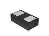
PESD5V0S1BL
DFN1006
Bi-directional ESD Protection Diode in DFN1006 Package
1.
Features
Capacitance: 15pF(typ.)
Reverse Working Voltage: 5V
IEC 61000-4-2 (ESD Air): ±25KV
2.
Pin Description
4.
Schematic Diagram
Datasheet
IEC 61000-4-2 (ESD Contact): ±25KV
IEC 61000-4-5 (Lightning 8/20µs): 8A
3.
5.
6.
Applications
Smart Phone and Tablet PC
TV and Set Top Box
Wearable Devices
PDA
Order Information
Type
Package
Size (mm)
Delivery Form
Delivery Quantity
P ESD5V0S1B L
DFN1006
1.00x0.60x0.37
7” T&R
10,000
Limiting Values(TA = 25 °C, unless otherwise specified)
Symbol
7.
Parameter
Conditions
Min
Max
Unit
IEC 61000-4-2; Contact Discharge
-
±25
kV
IEC 61000-4-2; Air Discharge
-
±25
kV
VESD
Electrostatic Discharge Voltage
PPP
Peak Pulse Power
tP = 8/20 µs
-
80
W
IPPM
Rated Peak Pulse Current
tP = 8/20 µs
-
8
A
TA
Ambient Temperature Range
-
-55
125
℃
Tstg
Storage Temperature Range
-
-55
150
℃
Electrical Characteristics(TA = 25 °C, unless otherwise specified)
Symbol
Parameter
Conditions
Reverse Working Voltage
TA = 25 °C
Breakdown Voltage
IR = 1mA; TA = 25 °C
IR
Reverse Leakage Current
VC
Clamping Voltage
CJ
Junction Capacitance
VRWM
VBR
Min
Typ.
Max
Unit
-
-
5.0
V
5.6
6.5
8.4
V
VRWM = 5V; TA = 25 °C
-
-
0.1
µA
IPP=1A, tP =8/20µs
-
-
6
V
IPP=8A, tP =8/20µs
-
-
10
V
VR = 0V, f = 1 MHz
-
15
18
pF
Jiangsu Weida Semiconductor Co., Ltd.
1/ 5
�PESD5V0S1BL
DFN1006
Bi-directional ESD Protection Diode in DFN1006 Package
8.
Datasheet
Typical Characteristics
Fig.1 Pulse Waveform-ESD (IEC61000-4-2)
Fig.2 Transmission Line Pulse (TLP)
Fig.3 V-I Characteristics for Bidirectional Diode
Fig.4 IV Curve
Fig.5 Clamping Voltage at IEC61000-4-2
Fig.6 Clamping Voltage at IEC61000-4-2
+8kV Pulse Waveform
-8kV Pulse Waveform
Jiangsu Weida Semiconductor Co., Ltd.
2/ 5
�PESD5V0S1BL
DFN1006
Bi-directional ESD Protection Diode in DFN1006 Package
9.
Datasheet
Package Outline Dimensions
DFN1006 Package Outline
Symbol
Dimensions In
Millimeters
Dimensions In
Inches
Min
Max
Min
Max
A
0.350
0.450
0.014
0.018
D
0.550
0.650
0.022
0.026
E
0.950
1.050
0.037
0.041
D1
0.420
0.520
0.017
0.020
E1
0.550
0.650
0.022
0.026
L
0.270
0.370
0.011
0.015
L1
0.000
0.100
0.000
0.004
Jiangsu Weida Semiconductor Co., Ltd.
3/ 5
�PESD5V0S1BL
DFN1006
Bi-directional ESD Protection Diode in DFN1006 Package
Soldering Parameters
FIG.5: Reflow condition
tp
TP
Critical Zone
TL to TP
Ramp-up
TL
tL
TS(max)
Temperature
10.
Datasheet
Ramp-down
Preheat
TS(min)
ts
25
time to peak temperatue
(t 25℃ to peak)
Reflow Condition
Pre-heat
Time
Pb-Free Assembly
-Temperature Min (Ts(min))
+150°C
-Temperature Max(Ts(max))
+200°C
-Time (Min to Max) (ts)
60-180 secs.
Average ramp up rate (Liquid us Temp (TL) to peak)
3°C/sec. Max
Ts(max) to TL - Ramp-up Rate
3°C/sec. Max
Reflow
-Temperature(TL)(Liquid us)
+217°C
-Temperature(tL)
60-150 secs.
Peak Temp (Tp)
+260(+0/-5)°C
Time within 5°C of actual Peak Temp (tp)
30 secs. Max
Ramp-down Rate
6°C/sec. Max
xTime 25°C to Peak Temp (TP)
8 min. Max
Do not exceed
+260°C
Jiangsu Weida Semiconductor Co., Ltd.
4/ 5
�PESD5V0S1BL
DFN1006
Bi-directional ESD Protection Diode in DFN1006 Package
11.
Datasheet
Contact Information
Online product information is available at www.wdsemi.com
Buy our products or get free samples,for further information and requests,
Please e-mail us at:sales1@wdsemi.com
12.
Copyrights & Disclaimer
Information furnished in this document is believed to be accurate and reliable. However, Jiangsu Weida
Semiconductor Co., Ltd assumes no responsibility for the consequences of use without consideration for
such information nor use beyond it.
Information mentioned in this document is subject to change without notice, apart from that when an
agreement is signed, Jiangsu Weida Semiconductor Co., Ltd complies with the agreement.
Products and information provided in this document have no infringement of patents. Jiangsu Weida
Semiconductor Co., Ltd assumes no responsibility for any infringement of other rights of third parties
which may result from the use of such products and information.
Jiangsu Weida Semiconductor Co., Ltd.
5/ 5
�
很抱歉,暂时无法提供与“PESD5V0S1BL”相匹配的价格&库存,您可以联系我们找货
免费人工找货- 国内价格
- 1+0.04050
- 30+0.03900
- 100+0.03750
- 500+0.03450
- 1000+0.03300
- 2000+0.03210


 工商网监
湘ICP备2023018690号
工商网监
湘ICP备2023018690号
