�
��
�� ���
eZ80AcclaimPlus!™ Connectivity ASSP
eZ80F91 ASSP
����
��������� � �
�
Product Specification
PS027006-1020
Copyright ©2020 Zilog, Inc. All rights reserved.
www.zilog.com
�eZ80F91 ASSP
Product Specification
ii
Warning: DO NOT USE THIS PRODUCT IN LIFE SUPPORT SYSTEMS.
LIFE SUPPORT POLICY
ZILOG’S PRODUCTS ARE NOT AUTHORIZED FOR USE AS CRITICAL COMPONENTS IN LIFE
SUPPORT DEVICES OR SYSTEMS WITHOUT THE EXPRESS PRIOR WRITTEN APPROVAL OF
THE PRESIDENT AND GENERAL COUNSEL OF ZILOG CORPORATION.
As used herein
Life support devices or systems are devices which (a) are intended for surgical implant into the body, or (b)
support or sustain life and whose failure to perform when properly used in accordance with instructions for
use provided in the labeling can be reasonably expected to result in a significant injury to the user. A critical component is any component in a life support device or system whose failure to perform can be reasonably expected to cause the failure of the life support device or system or to affect its safety or effectiveness.
Document Disclaimer
©2020 Zilog, Inc. All rights reserved. Information in this publication concerning the devices, applications,
or technology described is intended to suggest possible uses and may be superseded. ZILOG, INC. DOES
NOT ASSUME LIABILITY FOR OR PROVIDE A REPRESENTATION OF ACCURACY OF THE
INFORMATION, DEVICES, OR TECHNOLOGY DESCRIBED IN THIS DOCUMENT. ZILOG ALSO
DOES NOT ASSUME LIABILITY FOR INTELLECTUAL PROPERTY INFRINGEMENT RELATED
IN ANY MANNER TO USE OF INFORMATION, DEVICES, OR TECHNOLOGY DESCRIBED
HEREIN OR OTHERWISE. The information contained within this document has been verified according
to the general principles of electrical and mechanical engineering.
eZ80, eZ80AcclaimPlus!, Z80, Zdots, and Z180 are trademarks or registered trademarks of Zilog, Inc. All
other product or service names are the property of their respective owners.
PS027006-1020
PRELIMINARY
Disclaimer
�eZ80F91 ASSP
Product Specification
iii
Revision History
Each instance in the following revision history table reflects a change to this document
from its previous version. For more details, refer to the corresponding pages provided in
the table.
Date
Revision
Level
Description
Page
Number
Oct
2020
06
Removed BGA package. Updated environmental code for 144-LQFP pack- 1, 354,
age to “K” and removed code “C”.
355
Updated title page and headers to Littelfuse branding.
Various
Mar
2016
05
Added clarification about leap year compensation when BCD operation is
enabled in Chapter 10. Real Time Clock.
154
Jun
2013
04
Conditionally qualified the IRTC value in the DC Characteristics table.
338
May
2012
03
Updated to reference the eZ80AcclaimPlus! Development Kit
(eZ80F910300KITG).
354
Oct
2008
02
Updated Addressing section in I2C Serial I/O Interface chapter, Part Num- 46, 108,
ber Description, Figure 6, Flash Program Control Register, UART Transmit- 173, 198,
ter, and Figure 40.
220, 355
Jul
2007
01
Original Issue.
PS027006-1020
All
PRELIMINARY
Revision History
�eZ80F91 ASSP
Product Specification
iv
Table of Contents
Revision History . . . . . . . . . . . . . . . . . . . . . . . . . . . . . . . . . . . . . . . . . . . . . . . . . . . . . . . .iii
Table of Contents . . . . . . . . . . . . . . . . . . . . . . . . . . . . . . . . . . . . . . . . . . . . . . . . . . . . . . . iv
List of Figures . . . . . . . . . . . . . . . . . . . . . . . . . . . . . . . . . . . . . . . . . . . . . . . . . . . . . . . . . xv
List of Tables . . . . . . . . . . . . . . . . . . . . . . . . . . . . . . . . . . . . . . . . . . . . . . . . . . . . . . . . .xviii
Architectural Overview . . . . . . . . . . . . . . . . . . . . . . . . . . . . . . . . . . . . . . . . . . . . . . . . . . . 1
Features . . . . . . . . . . . . . . . . . . . . . . . . . . . . . . . . . . . . . . . . . . . . . . . . . . . . . . . . . . . . 1
Block Diagram . . . . . . . . . . . . . . . . . . . . . . . . . . . . . . . . . . . . . . . . . . . . . . . . . . . . . . 2
Pin Description . . . . . . . . . . . . . . . . . . . . . . . . . . . . . . . . . . . . . . . . . . . . . . . . . . . . . . 4
Pin Characteristics . . . . . . . . . . . . . . . . . . . . . . . . . . . . . . . . . . . . . . . . . . . . . . . . . . . 5
System Clock Source Options . . . . . . . . . . . . . . . . . . . . . . . . . . . . . . . . . . . . . . . . . 24
SCLK Source Selection Example . . . . . . . . . . . . . . . . . . . . . . . . . . . . . . . . . . . . 24
Register Map . . . . . . . . . . . . . . . . . . . . . . . . . . . . . . . . . . . . . . . . . . . . . . . . . . . . . . . . . . 25
eZ80 CPU Core . . . . . . . . . . . . . . . . . . . . . . . . . . . . . . . . . . . . . . . . . . . . . . . . . . . . . . . . 36
Features . . . . . . . . . . . . . . . . . . . . . . . . . . . . . . . . . . . . . . . . . . . . . . . . . . . . . . . . . . . 36
New Instructions . . . . . . . . . . . . . . . . . . . . . . . . . . . . . . . . . . . . . . . . . . . . . . . . . . . . 36
Reset . . . . . . . . . . . . . . . . . . . . . . . . . . . . . . . . . . . . . . . . . . . . . . . . . . . . . . . . . . . . . . . .
External Reset Input and Indicator . . . . . . . . . . . . . . . . . . . . . . . . . . . . . . . . . . . . . .
Power-On Reset . . . . . . . . . . . . . . . . . . . . . . . . . . . . . . . . . . . . . . . . . . . . . . . . . . . .
Voltage Brown-Out Reset . . . . . . . . . . . . . . . . . . . . . . . . . . . . . . . . . . . . . . . . . . . . .
37
37
38
38
Low-Power Modes . . . . . . . . . . . . . . . . . . . . . . . . . . . . . . . . . . . . . . . . . . . . . . . . . . . . .
SLEEP Mode . . . . . . . . . . . . . . . . . . . . . . . . . . . . . . . . . . . . . . . . . . . . . . . . . . . . . .
HALT Mode . . . . . . . . . . . . . . . . . . . . . . . . . . . . . . . . . . . . . . . . . . . . . . . . . . . . . . .
HALT Mode and the EMAC Function . . . . . . . . . . . . . . . . . . . . . . . . . . . . . . . .
Clock Peripheral Power-Down Registers . . . . . . . . . . . . . . . . . . . . . . . . . . . . . . . . .
40
40
40
41
41
General-Purpose Input/Output . . . . . . . . . . . . . . . . . . . . . . . . . . . . . . . . . . . . . . . . . . . . .
GPIO Operation . . . . . . . . . . . . . . . . . . . . . . . . . . . . . . . . . . . . . . . . . . . . . . . . . . . .
GPIO Interrupts . . . . . . . . . . . . . . . . . . . . . . . . . . . . . . . . . . . . . . . . . . . . . . . . . . . . .
Level-Triggered Interrupts . . . . . . . . . . . . . . . . . . . . . . . . . . . . . . . . . . . . . . . . .
Edge-Triggered Interrupts . . . . . . . . . . . . . . . . . . . . . . . . . . . . . . . . . . . . . . . . .
GPIO Control Registers . . . . . . . . . . . . . . . . . . . . . . . . . . . . . . . . . . . . . . . . . . . . . .
Port x Data Registers . . . . . . . . . . . . . . . . . . . . . . . . . . . . . . . . . . . . . . . . . . . . .
Port x Data Direction Registers . . . . . . . . . . . . . . . . . . . . . . . . . . . . . . . . . . . . .
44
44
49
49
49
50
50
51
PS027006-1020
PRELIMINARY
Table of Contents
�eZ80F91 ASSP
Product Specification
v
Port x Alternate Register 0 . . . . . . . . . . . . . . . . . . . . . . . . . . . . . . . . . . . . . . . . . 51
Port x Alternate Register 1 . . . . . . . . . . . . . . . . . . . . . . . . . . . . . . . . . . . . . . . . . 52
Port x Alternate Register 2 . . . . . . . . . . . . . . . . . . . . . . . . . . . . . . . . . . . . . . . . . 52
Interrupt Controller . . . . . . . . . . . . . . . . . . . . . . . . . . . . . . . . . . . . . . . . . . . . . . . . . . . . .
Maskable Interrupts . . . . . . . . . . . . . . . . . . . . . . . . . . . . . . . . . . . . . . . . . . . . . . . . .
Interrupt Priority Registers . . . . . . . . . . . . . . . . . . . . . . . . . . . . . . . . . . . . . . . . .
GPIO Port Interrupts . . . . . . . . . . . . . . . . . . . . . . . . . . . . . . . . . . . . . . . . . . . . . . . . .
53
53
56
59
Chip Selects and Wait States . . . . . . . . . . . . . . . . . . . . . . . . . . . . . . . . . . . . . . . . . . . . . .
Memory and I/O Chip Selects . . . . . . . . . . . . . . . . . . . . . . . . . . . . . . . . . . . . . . . . . .
Memory Chip Select Operation . . . . . . . . . . . . . . . . . . . . . . . . . . . . . . . . . . . . . . . .
Memory Chip Select Priority . . . . . . . . . . . . . . . . . . . . . . . . . . . . . . . . . . . . . . .
Reset States . . . . . . . . . . . . . . . . . . . . . . . . . . . . . . . . . . . . . . . . . . . . . . . . . . . . .
Memory Chip Select Example . . . . . . . . . . . . . . . . . . . . . . . . . . . . . . . . . . . . . .
Input/Output Chip Select Operation . . . . . . . . . . . . . . . . . . . . . . . . . . . . . . . . . . . . .
Wait States . . . . . . . . . . . . . . . . . . . . . . . . . . . . . . . . . . . . . . . . . . . . . . . . . . . . . . . .
WAIT Input Signal . . . . . . . . . . . . . . . . . . . . . . . . . . . . . . . . . . . . . . . . . . . . . . . . . .
Chip Selects During Bus Request/Bus Acknowledge Cycles . . . . . . . . . . . . . . . . . .
Bus Mode Controller . . . . . . . . . . . . . . . . . . . . . . . . . . . . . . . . . . . . . . . . . . . . . . . . .
eZ80 BUS Mode . . . . . . . . . . . . . . . . . . . . . . . . . . . . . . . . . . . . . . . . . . . . . . . . . . . .
Z80 BUS Mode . . . . . . . . . . . . . . . . . . . . . . . . . . . . . . . . . . . . . . . . . . . . . . . . . . . . .
Intel Bus Mode . . . . . . . . . . . . . . . . . . . . . . . . . . . . . . . . . . . . . . . . . . . . . . . . . . . . .
Intel Bus Mode: Separate Address and Data Buses . . . . . . . . . . . . . . . . . . . . . .
Intel Bus Mode: Multiplexed Address and Data Bus . . . . . . . . . . . . . . . . . . . . .
Motorola Bus Mode . . . . . . . . . . . . . . . . . . . . . . . . . . . . . . . . . . . . . . . . . . . . . . . . .
Switching Between Bus Modes . . . . . . . . . . . . . . . . . . . . . . . . . . . . . . . . . . . . .
Chip Select Registers . . . . . . . . . . . . . . . . . . . . . . . . . . . . . . . . . . . . . . . . . . . . . . . .
Chip Select x Lower Bound Register . . . . . . . . . . . . . . . . . . . . . . . . . . . . . . . . .
Chip Select x Upper Bound Register . . . . . . . . . . . . . . . . . . . . . . . . . . . . . . . . .
Chip Select x Control Register . . . . . . . . . . . . . . . . . . . . . . . . . . . . . . . . . . . . . .
Chip Select x Bus Mode Control Register . . . . . . . . . . . . . . . . . . . . . . . . . . . . .
Bus Arbiter . . . . . . . . . . . . . . . . . . . . . . . . . . . . . . . . . . . . . . . . . . . . . . . . . . . . . . . .
61
61
61
62
62
62
64
64
65
66
67
67
67
70
71
75
78
81
82
82
83
84
85
86
Random Access Memory . . . . . . . . . . . . . . . . . . . . . . . . . . . . . . . . . . . . . . . . . . . . . . . .
RAM Control Registers . . . . . . . . . . . . . . . . . . . . . . . . . . . . . . . . . . . . . . . . . . . . . .
RAM Control Register . . . . . . . . . . . . . . . . . . . . . . . . . . . . . . . . . . . . . . . . . . . .
RAM Address Upper Byte Register . . . . . . . . . . . . . . . . . . . . . . . . . . . . . . . . . .
MBIST Control . . . . . . . . . . . . . . . . . . . . . . . . . . . . . . . . . . . . . . . . . . . . . . . . . .
89
90
90
91
92
Flash Memory . . . . . . . . . . . . . . . . . . . . . . . . . . . . . . . . . . . . . . . . . . . . . . . . . . . . . . . . . 93
PS027006-1020
PRELIMINARY
Table of Contents
�eZ80F91 ASSP
Product Specification
vi
Flash Memory Overview . . . . . . . . . . . . . . . . . . . . . . . . . . . . . . . . . . . . . . . . . . . . . 94
Reading Flash Memory . . . . . . . . . . . . . . . . . . . . . . . . . . . . . . . . . . . . . . . . . . . . . . . 94
Memory Read . . . . . . . . . . . . . . . . . . . . . . . . . . . . . . . . . . . . . . . . . . . . . . . . . . . . . . 95
I/O Read . . . . . . . . . . . . . . . . . . . . . . . . . . . . . . . . . . . . . . . . . . . . . . . . . . . . . . . 95
Programming Flash Memory . . . . . . . . . . . . . . . . . . . . . . . . . . . . . . . . . . . . . . . . . . 95
Single-Byte I/O Write . . . . . . . . . . . . . . . . . . . . . . . . . . . . . . . . . . . . . . . . . . . . 95
Multibyte I/O Write (Row Programming) . . . . . . . . . . . . . . . . . . . . . . . . . . . . . 96
Memory Write . . . . . . . . . . . . . . . . . . . . . . . . . . . . . . . . . . . . . . . . . . . . . . . . . . 97
Erasing Flash Memory . . . . . . . . . . . . . . . . . . . . . . . . . . . . . . . . . . . . . . . . . . . . . . . 97
Mass Erase . . . . . . . . . . . . . . . . . . . . . . . . . . . . . . . . . . . . . . . . . . . . . . . . . . . . . 97
Page Erase . . . . . . . . . . . . . . . . . . . . . . . . . . . . . . . . . . . . . . . . . . . . . . . . . . . . . 97
Information Page Characteristics . . . . . . . . . . . . . . . . . . . . . . . . . . . . . . . . . . . . . . . 98
Flash Control Registers . . . . . . . . . . . . . . . . . . . . . . . . . . . . . . . . . . . . . . . . . . . . . . . 98
Flash Key Register . . . . . . . . . . . . . . . . . . . . . . . . . . . . . . . . . . . . . . . . . . . . . . . 98
Flash Data Register . . . . . . . . . . . . . . . . . . . . . . . . . . . . . . . . . . . . . . . . . . . . . . 99
Flash Address Upper Byte Register . . . . . . . . . . . . . . . . . . . . . . . . . . . . . . . . . 100
Flash Control Register . . . . . . . . . . . . . . . . . . . . . . . . . . . . . . . . . . . . . . . . . . . 101
Flash Frequency Divider Register . . . . . . . . . . . . . . . . . . . . . . . . . . . . . . . . . . 102
Flash Write/Erase Protection Register . . . . . . . . . . . . . . . . . . . . . . . . . . . . . . . 103
Flash Interrupt Control Register . . . . . . . . . . . . . . . . . . . . . . . . . . . . . . . . . . . . 104
Flash Page Select Register . . . . . . . . . . . . . . . . . . . . . . . . . . . . . . . . . . . . . . . . 106
Flash Row Select Register . . . . . . . . . . . . . . . . . . . . . . . . . . . . . . . . . . . . . . . . 107
Flash Column Select Register . . . . . . . . . . . . . . . . . . . . . . . . . . . . . . . . . . . . . 108
Flash Program Control Register . . . . . . . . . . . . . . . . . . . . . . . . . . . . . . . . . . . . 108
Watchdog Timer . . . . . . . . . . . . . . . . . . . . . . . . . . . . . . . . . . . . . . . . . . . . . . . . . . . . . .
Watchdog Timer Operation . . . . . . . . . . . . . . . . . . . . . . . . . . . . . . . . . . . . . . . . . .
Enabling and Disabling the Watchdog Timer . . . . . . . . . . . . . . . . . . . . . . . . .
Time-Out Period Selection . . . . . . . . . . . . . . . . . . . . . . . . . . . . . . . . . . . . . . . .
RESET or NMI Generation . . . . . . . . . . . . . . . . . . . . . . . . . . . . . . . . . . . . . . .
Watchdog Timer Registers . . . . . . . . . . . . . . . . . . . . . . . . . . . . . . . . . . . . . . . . . . .
Watchdog Timer Control Register . . . . . . . . . . . . . . . . . . . . . . . . . . . . . . . . . .
Watchdog Timer Reset Register . . . . . . . . . . . . . . . . . . . . . . . . . . . . . . . . . . . .
110
111
111
111
112
112
112
115
Programmable Reload Timers . . . . . . . . . . . . . . . . . . . . . . . . . . . . . . . . . . . . . . . . . . . .
Basic Timer Operation . . . . . . . . . . . . . . . . . . . . . . . . . . . . . . . . . . . . . . . . . . . . . .
Reading the Current Count Value . . . . . . . . . . . . . . . . . . . . . . . . . . . . . . . . . .
Setting Timer Duration . . . . . . . . . . . . . . . . . . . . . . . . . . . . . . . . . . . . . . . . . . .
SINGLE PASS Mode . . . . . . . . . . . . . . . . . . . . . . . . . . . . . . . . . . . . . . . . . . . .
CONTINUOUS Mode . . . . . . . . . . . . . . . . . . . . . . . . . . . . . . . . . . . . . . . . . . .
Timer Interrupts . . . . . . . . . . . . . . . . . . . . . . . . . . . . . . . . . . . . . . . . . . . . . . . .
116
117
117
117
118
118
119
PS027006-1020
PRELIMINARY
Table of Contents
�eZ80F91 ASSP
Product Specification
vii
Timer Input Source Selection . . . . . . . . . . . . . . . . . . . . . . . . . . . . . . . . . . . . . .
Timer Output . . . . . . . . . . . . . . . . . . . . . . . . . . . . . . . . . . . . . . . . . . . . . . . . . .
Break Point Halting . . . . . . . . . . . . . . . . . . . . . . . . . . . . . . . . . . . . . . . . . . . . .
Specialty Timer Modes . . . . . . . . . . . . . . . . . . . . . . . . . . . . . . . . . . . . . . . . . . . . . .
Event Counter . . . . . . . . . . . . . . . . . . . . . . . . . . . . . . . . . . . . . . . . . . . . . . . . . .
RTC Oscillator Input . . . . . . . . . . . . . . . . . . . . . . . . . . . . . . . . . . . . . . . . . . . .
Input Capture . . . . . . . . . . . . . . . . . . . . . . . . . . . . . . . . . . . . . . . . . . . . . . . . . .
Output Compare . . . . . . . . . . . . . . . . . . . . . . . . . . . . . . . . . . . . . . . . . . . . . . . .
Timer Port Pin Allocation . . . . . . . . . . . . . . . . . . . . . . . . . . . . . . . . . . . . . . . . . . . .
Timer Registers . . . . . . . . . . . . . . . . . . . . . . . . . . . . . . . . . . . . . . . . . . . . . . . . . . . .
Basic Timer Register Set . . . . . . . . . . . . . . . . . . . . . . . . . . . . . . . . . . . . . . . . .
Register Set for Capture in Timer 1 . . . . . . . . . . . . . . . . . . . . . . . . . . . . . . . . .
Register Set for Capture/Compare/PWM in Timer 3 . . . . . . . . . . . . . . . . . . . .
Timer Control Register . . . . . . . . . . . . . . . . . . . . . . . . . . . . . . . . . . . . . . . . . . .
Timer Interrupt Enable Register . . . . . . . . . . . . . . . . . . . . . . . . . . . . . . . . . . . .
Timer Interrupt Identification Register . . . . . . . . . . . . . . . . . . . . . . . . . . . . . .
Timer Data Low Byte Register . . . . . . . . . . . . . . . . . . . . . . . . . . . . . . . . . . . .
Timer Data High Byte Register . . . . . . . . . . . . . . . . . . . . . . . . . . . . . . . . . . . .
Timer Reload Low Byte Register . . . . . . . . . . . . . . . . . . . . . . . . . . . . . . . . . . .
Timer Reload High Byte Register . . . . . . . . . . . . . . . . . . . . . . . . . . . . . . . . . .
Timer Input Capture Control Register . . . . . . . . . . . . . . . . . . . . . . . . . . . . . . .
Timer Input Capture Value A Low Byte Register . . . . . . . . . . . . . . . . . . . . . .
Timer Input Capture Value A High Byte Register . . . . . . . . . . . . . . . . . . . . . .
Timer Input Capture Value B Low Byte Register . . . . . . . . . . . . . . . . . . . . . .
Timer Input Capture Value B High Byte Register . . . . . . . . . . . . . . . . . . . . . .
Timer Output Compare Control Register 1 . . . . . . . . . . . . . . . . . . . . . . . . . . .
Timer Output Compare Control Register 2 . . . . . . . . . . . . . . . . . . . . . . . . . . .
Timer Output Compare Value Low Byte Register . . . . . . . . . . . . . . . . . . . . . .
Timer Output Compare Value High Byte Register . . . . . . . . . . . . . . . . . . . . .
Multi-PWM Mode . . . . . . . . . . . . . . . . . . . . . . . . . . . . . . . . . . . . . . . . . . . . . . . . .
PWM Master Mode . . . . . . . . . . . . . . . . . . . . . . . . . . . . . . . . . . . . . . . . . . . . . . . . .
Modification of Edge Transition Values . . . . . . . . . . . . . . . . . . . . . . . . . . . . . . . . .
AND/OR Gating of the PWM Outputs . . . . . . . . . . . . . . . . . . . . . . . . . . . . . . . . . .
PWM Nonoverlapping Output Pair Delays . . . . . . . . . . . . . . . . . . . . . . . . . . . . . .
Multi-PWM Power-Trip Mode . . . . . . . . . . . . . . . . . . . . . . . . . . . . . . . . . . . . . . . .
Multi-PWM Control Registers . . . . . . . . . . . . . . . . . . . . . . . . . . . . . . . . . . . . . . . .
Pulse-Width Modulation Control Register 1 . . . . . . . . . . . . . . . . . . . . . . . . . .
Pulse-Width Modulation Control Register 2 . . . . . . . . . . . . . . . . . . . . . . . . . .
Pulse-Width Modulation Control Register 3 . . . . . . . . . . . . . . . . . . . . . . . . . .
PS027006-1020
PRELIMINARY
120
120
121
121
122
122
122
123
123
124
124
125
125
127
128
129
130
132
133
133
134
135
136
136
137
137
138
139
140
140
143
143
144
145
147
148
148
149
151
Table of Contents
�eZ80F91 ASSP
Product Specification
viii
Pulse-Width Modulation Rising Edge Low Byte Register
Pulse-Width Modulation Rising Edge High Byte Register
Pulse-Width Modulation Falling Edge Low Byte Register
Pulse-Width Modulation Falling Edge High Byte Register
...............
...............
...............
...............
152
152
153
153
Real-Time Clock . . . . . . . . . . . . . . . . . . . . . . . . . . . . . . . . . . . . . . . . . . . . . . . . . . . . . .
Real-Time Clock Alarm . . . . . . . . . . . . . . . . . . . . . . . . . . . . . . . . . . . . . . . . . . . . .
Real-Time Clock Oscillator and Source Selection . . . . . . . . . . . . . . . . . . . . . . . . .
Real-Time Clock Battery Backup . . . . . . . . . . . . . . . . . . . . . . . . . . . . . . . . . . . . . .
Real-Time Clock Recommended Operation . . . . . . . . . . . . . . . . . . . . . . . . . . . . . .
Real-Time Clock Registers . . . . . . . . . . . . . . . . . . . . . . . . . . . . . . . . . . . . . . . . . . .
Real-Time Clock Seconds Register . . . . . . . . . . . . . . . . . . . . . . . . . . . . . . . . .
Real-Time Clock Minutes Register . . . . . . . . . . . . . . . . . . . . . . . . . . . . . . . . .
Real-Time Clock Hours Register . . . . . . . . . . . . . . . . . . . . . . . . . . . . . . . . . . .
Real-Time Clock Day-of-the-Week Register . . . . . . . . . . . . . . . . . . . . . . . . . .
Real-Time Clock Day-of-the-Month Register . . . . . . . . . . . . . . . . . . . . . . . . .
Real-Time Clock Month Register . . . . . . . . . . . . . . . . . . . . . . . . . . . . . . . . . .
Real-Time Clock Year Register . . . . . . . . . . . . . . . . . . . . . . . . . . . . . . . . . . . .
Real-Time Clock Century Register . . . . . . . . . . . . . . . . . . . . . . . . . . . . . . . . .
Real-Time Clock Alarm Seconds Register . . . . . . . . . . . . . . . . . . . . . . . . . . .
Real-Time Clock Alarm Minutes Register . . . . . . . . . . . . . . . . . . . . . . . . . . . .
Real-Time Clock Alarm Hours Register . . . . . . . . . . . . . . . . . . . . . . . . . . . . .
Real-Time Clock Alarm Day-of-the-Week Register . . . . . . . . . . . . . . . . . . . .
Real-Time Clock Alarm Control Register . . . . . . . . . . . . . . . . . . . . . . . . . . . .
Real-Time Clock Control Register . . . . . . . . . . . . . . . . . . . . . . . . . . . . . . . . . .
154
155
156
156
156
156
157
157
159
160
161
162
163
164
165
166
167
168
169
170
Universal Asynchronous Receiver/Transmitter . . . . . . . . . . . . . . . . . . . . . . . . . . . . . .
UART Functional Description . . . . . . . . . . . . . . . . . . . . . . . . . . . . . . . . . . . . . . . .
UART Functions . . . . . . . . . . . . . . . . . . . . . . . . . . . . . . . . . . . . . . . . . . . . . . . . . . .
UART Transmitter . . . . . . . . . . . . . . . . . . . . . . . . . . . . . . . . . . . . . . . . . . . . . .
UART Receiver . . . . . . . . . . . . . . . . . . . . . . . . . . . . . . . . . . . . . . . . . . . . . . . .
UART Modem Control . . . . . . . . . . . . . . . . . . . . . . . . . . . . . . . . . . . . . . . . . .
UART Interrupts . . . . . . . . . . . . . . . . . . . . . . . . . . . . . . . . . . . . . . . . . . . . . . . . . . .
UART Transmitter Interrupt . . . . . . . . . . . . . . . . . . . . . . . . . . . . . . . . . . . . . .
UART Receiver Interrupts . . . . . . . . . . . . . . . . . . . . . . . . . . . . . . . . . . . . . . . .
UART Modem Status Interrupt . . . . . . . . . . . . . . . . . . . . . . . . . . . . . . . . . . . .
UART Recommended Usage . . . . . . . . . . . . . . . . . . . . . . . . . . . . . . . . . . . . . . . . .
Module Reset . . . . . . . . . . . . . . . . . . . . . . . . . . . . . . . . . . . . . . . . . . . . . . . . . .
Control Transfers to Configure UART Operation . . . . . . . . . . . . . . . . . . . . . .
Data Transfers . . . . . . . . . . . . . . . . . . . . . . . . . . . . . . . . . . . . . . . . . . . . . . . . .
Baud Rate Generator . . . . . . . . . . . . . . . . . . . . . . . . . . . . . . . . . . . . . . . . . . . . . . . .
172
173
173
173
174
174
175
175
175
176
176
176
176
177
178
PS027006-1020
PRELIMINARY
Table of Contents
�eZ80F91 ASSP
Product Specification
ix
Recommended Use of the Baud Rate Generator . . . . . . . . . . . . . . . . . . . . . . .
BRG Control Registers . . . . . . . . . . . . . . . . . . . . . . . . . . . . . . . . . . . . . . . . . . . . . .
UART Baud Rate Generator High and Low Byte Registers . . . . . . . . . . . . . .
UART Registers . . . . . . . . . . . . . . . . . . . . . . . . . . . . . . . . . . . . . . . . . . . . . . . . . . .
UART Transmit Holding Register . . . . . . . . . . . . . . . . . . . . . . . . . . . . . . . . . .
UART Receive Buffer Register . . . . . . . . . . . . . . . . . . . . . . . . . . . . . . . . . . . .
UART Interrupt Enable Register . . . . . . . . . . . . . . . . . . . . . . . . . . . . . . . . . . .
UART Interrupt Identification Register . . . . . . . . . . . . . . . . . . . . . . . . . . . . . .
UART FIFO Control Register . . . . . . . . . . . . . . . . . . . . . . . . . . . . . . . . . . . . .
UART Line Control Register . . . . . . . . . . . . . . . . . . . . . . . . . . . . . . . . . . . . . .
UART Modem Control Register . . . . . . . . . . . . . . . . . . . . . . . . . . . . . . . . . . .
UART Line Status Register . . . . . . . . . . . . . . . . . . . . . . . . . . . . . . . . . . . . . . .
UART Modem Status Register . . . . . . . . . . . . . . . . . . . . . . . . . . . . . . . . . . . . .
UART Scratch Pad Register . . . . . . . . . . . . . . . . . . . . . . . . . . . . . . . . . . . . . . .
179
179
179
181
181
182
182
183
185
186
188
189
191
192
Infrared Encoder/Decoder . . . . . . . . . . . . . . . . . . . . . . . . . . . . . . . . . . . . . . . . . . . . . . .
Functional Description . . . . . . . . . . . . . . . . . . . . . . . . . . . . . . . . . . . . . . . . . . . . . .
Transmit . . . . . . . . . . . . . . . . . . . . . . . . . . . . . . . . . . . . . . . . . . . . . . . . . . . . . . . . .
Receive . . . . . . . . . . . . . . . . . . . . . . . . . . . . . . . . . . . . . . . . . . . . . . . . . . . . . . . . . .
Jitter . . . . . . . . . . . . . . . . . . . . . . . . . . . . . . . . . . . . . . . . . . . . . . . . . . . . . . . . . . . . .
Infrared Encoder/Decoder Signal Pins . . . . . . . . . . . . . . . . . . . . . . . . . . . . . . . . . .
Loopback Testing . . . . . . . . . . . . . . . . . . . . . . . . . . . . . . . . . . . . . . . . . . . . . . . . . .
Infrared Encoder/Decoder Register . . . . . . . . . . . . . . . . . . . . . . . . . . . . . . . . .
193
193
194
194
196
196
196
197
Serial Peripheral Interface . . . . . . . . . . . . . . . . . . . . . . . . . . . . . . . . . . . . . . . . . . . . . . .
SPI Signals . . . . . . . . . . . . . . . . . . . . . . . . . . . . . . . . . . . . . . . . . . . . . . . . . . . . . . .
Master In, Slave Out . . . . . . . . . . . . . . . . . . . . . . . . . . . . . . . . . . . . . . . . . . . . .
Master Out, Slave In . . . . . . . . . . . . . . . . . . . . . . . . . . . . . . . . . . . . . . . . . . . . .
Slave Select . . . . . . . . . . . . . . . . . . . . . . . . . . . . . . . . . . . . . . . . . . . . . . . . . . .
Serial Clock . . . . . . . . . . . . . . . . . . . . . . . . . . . . . . . . . . . . . . . . . . . . . . . . . . .
SPI Functional Description . . . . . . . . . . . . . . . . . . . . . . . . . . . . . . . . . . . . . . . . . . .
SPI Flags . . . . . . . . . . . . . . . . . . . . . . . . . . . . . . . . . . . . . . . . . . . . . . . . . . . . . . . . .
Mode Fault . . . . . . . . . . . . . . . . . . . . . . . . . . . . . . . . . . . . . . . . . . . . . . . . . . . .
Write Collision . . . . . . . . . . . . . . . . . . . . . . . . . . . . . . . . . . . . . . . . . . . . . . . . .
SPI Baud Rate Generator . . . . . . . . . . . . . . . . . . . . . . . . . . . . . . . . . . . . . . . . . . . .
Baud Rate Generator Functional Description . . . . . . . . . . . . . . . . . . . . . . . . .
Data Transfer Procedure with SPI Configured as a Master . . . . . . . . . . . . . . . . . .
Data Transfer Procedure with SPI Configured as a Slave . . . . . . . . . . . . . . . . . . .
SPI Registers . . . . . . . . . . . . . . . . . . . . . . . . . . . . . . . . . . . . . . . . . . . . . . . . . . . . . .
SPI Baud Rate Generator Low Byte and High Byte Registers . . . . . . . . . . . .
198
199
199
199
199
200
201
202
202
202
202
202
203
203
203
204
PS027006-1020
PRELIMINARY
Table of Contents
�eZ80F91 ASSP
Product Specification
x
SPI Control Register . . . . . . . . . . . . . . . . . . . . . . . . . . . . . . . . . . . . . . . . . . . . .
SPI Status Register . . . . . . . . . . . . . . . . . . . . . . . . . . . . . . . . . . . . . . . . . . . . . .
SPI Transmit Shift Register . . . . . . . . . . . . . . . . . . . . . . . . . . . . . . . . . . . . . . .
SPI Receive Buffer Register . . . . . . . . . . . . . . . . . . . . . . . . . . . . . . . . . . . . . . .
205
206
207
208
I2C Serial I/O Interface . . . . . . . . . . . . . . . . . . . . . . . . . . . . . . . . . . . . . . . . . . . . . . . . .
Clocking Overview . . . . . . . . . . . . . . . . . . . . . . . . . . . . . . . . . . . . . . . . . . . . . .
Bus Arbitration Overview . . . . . . . . . . . . . . . . . . . . . . . . . . . . . . . . . . . . . . . .
Data Validity . . . . . . . . . . . . . . . . . . . . . . . . . . . . . . . . . . . . . . . . . . . . . . . . . .
Start and Stop Conditions . . . . . . . . . . . . . . . . . . . . . . . . . . . . . . . . . . . . . . . . .
Transferring Data . . . . . . . . . . . . . . . . . . . . . . . . . . . . . . . . . . . . . . . . . . . . . . . . . .
Byte Format . . . . . . . . . . . . . . . . . . . . . . . . . . . . . . . . . . . . . . . . . . . . . . . . . . .
Acknowledge . . . . . . . . . . . . . . . . . . . . . . . . . . . . . . . . . . . . . . . . . . . . . . . . . .
Clock Synchronization . . . . . . . . . . . . . . . . . . . . . . . . . . . . . . . . . . . . . . . . . . . . . .
Arbitration . . . . . . . . . . . . . . . . . . . . . . . . . . . . . . . . . . . . . . . . . . . . . . . . . . . .
Clock Synchronization for Handshake . . . . . . . . . . . . . . . . . . . . . . . . . . . . . . .
Operating Modes . . . . . . . . . . . . . . . . . . . . . . . . . . . . . . . . . . . . . . . . . . . . . . . . . . .
Master Transmit . . . . . . . . . . . . . . . . . . . . . . . . . . . . . . . . . . . . . . . . . . . . . . . .
Master Receive . . . . . . . . . . . . . . . . . . . . . . . . . . . . . . . . . . . . . . . . . . . . . . . . .
Slave Transmit . . . . . . . . . . . . . . . . . . . . . . . . . . . . . . . . . . . . . . . . . . . . . . . . .
Slave Receive . . . . . . . . . . . . . . . . . . . . . . . . . . . . . . . . . . . . . . . . . . . . . . . . . .
I2C Registers . . . . . . . . . . . . . . . . . . . . . . . . . . . . . . . . . . . . . . . . . . . . . . . . . . . . . .
Addressing . . . . . . . . . . . . . . . . . . . . . . . . . . . . . . . . . . . . . . . . . . . . . . . . . . . .
2
Resetting the I C Registers . . . . . . . . . . . . . . . . . . . . . . . . . . . . . . . . . . . . . . .
2
I C Slave Address Register . . . . . . . . . . . . . . . . . . . . . . . . . . . . . . . . . . . . . . .
I2C Extended Slave Address Register . . . . . . . . . . . . . . . . . . . . . . . . . . . . . . .
2
I C Data Register . . . . . . . . . . . . . . . . . . . . . . . . . . . . . . . . . . . . . . . . . . . . . . .
2
I C Control Register . . . . . . . . . . . . . . . . . . . . . . . . . . . . . . . . . . . . . . . . . . . .
2
I C Status Register . . . . . . . . . . . . . . . . . . . . . . . . . . . . . . . . . . . . . . . . . . . . . .
2
I C Clock Control Register . . . . . . . . . . . . . . . . . . . . . . . . . . . . . . . . . . . . . . .
Bus Clock Speed . . . . . . . . . . . . . . . . . . . . . . . . . . . . . . . . . . . . . . . . . . . . . . .
2
I C Software Reset Register . . . . . . . . . . . . . . . . . . . . . . . . . . . . . . . . . . . . . .
209
209
209
210
210
211
211
211
212
213
214
214
214
217
219
219
220
220
221
221
222
223
223
226
228
229
229
Zilog Debug Interface . . . . . . . . . . . . . . . . . . . . . . . . . . . . . . . . . . . . . . . . . . . . . . . . . .
ZDI-Supported Protocol . . . . . . . . . . . . . . . . . . . . . . . . . . . . . . . . . . . . . . . . . . . . .
ZDI Clock and Data Conventions . . . . . . . . . . . . . . . . . . . . . . . . . . . . . . . . . . . . . .
ZDI Start Condition . . . . . . . . . . . . . . . . . . . . . . . . . . . . . . . . . . . . . . . . . . . . . . . .
ZDI Single-Bit Byte Separator . . . . . . . . . . . . . . . . . . . . . . . . . . . . . . . . . . . . .
ZDI Register Addressing . . . . . . . . . . . . . . . . . . . . . . . . . . . . . . . . . . . . . . . . . . . .
ZDI Write Operations . . . . . . . . . . . . . . . . . . . . . . . . . . . . . . . . . . . . . . . . . . . . . . .
ZDI Single-Byte Write . . . . . . . . . . . . . . . . . . . . . . . . . . . . . . . . . . . . . . . . . . .
230
231
232
232
233
234
235
235
PS027006-1020
PRELIMINARY
Table of Contents
�eZ80F91 ASSP
Product Specification
xi
ZDI Block Write . . . . . . . . . . . . . . . . . . . . . . . . . . . . . . . . . . . . . . . . . . . . . . . .
ZDI Read Operations . . . . . . . . . . . . . . . . . . . . . . . . . . . . . . . . . . . . . . . . . . . . . . .
ZDI Single-Byte Read . . . . . . . . . . . . . . . . . . . . . . . . . . . . . . . . . . . . . . . . . . .
ZDI Block Read . . . . . . . . . . . . . . . . . . . . . . . . . . . . . . . . . . . . . . . . . . . . . . . .
Operation of the eZ80F91 Device During ZDI Break Points . . . . . . . . . . . . . . . . .
Bus Requests During ZDI Debug Mode . . . . . . . . . . . . . . . . . . . . . . . . . . . . . . . . .
Potential Hazards of Enabling Bus Requests During DEBUG Mode . . . . . . .
ZDI Write-Only Registers . . . . . . . . . . . . . . . . . . . . . . . . . . . . . . . . . . . . . . . . . . . .
ZDI Read-Only Registers . . . . . . . . . . . . . . . . . . . . . . . . . . . . . . . . . . . . . . . . . . . .
ZDI Register Definitions . . . . . . . . . . . . . . . . . . . . . . . . . . . . . . . . . . . . . . . . . . . . .
ZDI Address Match Registers . . . . . . . . . . . . . . . . . . . . . . . . . . . . . . . . . . . . .
ZDI Break Control Register . . . . . . . . . . . . . . . . . . . . . . . . . . . . . . . . . . . . . . .
ZDI Master Control Register . . . . . . . . . . . . . . . . . . . . . . . . . . . . . . . . . . . . . .
ZDI Write Data Registers . . . . . . . . . . . . . . . . . . . . . . . . . . . . . . . . . . . . . . . . .
ZDI Read/Write Control Register . . . . . . . . . . . . . . . . . . . . . . . . . . . . . . . . . .
ZDI Bus Control Register . . . . . . . . . . . . . . . . . . . . . . . . . . . . . . . . . . . . . . . . .
Instruction Store 4:0 Registers . . . . . . . . . . . . . . . . . . . . . . . . . . . . . . . . . . . . .
ZDI Write Memory Register . . . . . . . . . . . . . . . . . . . . . . . . . . . . . . . . . . . . . .
eZ80 Product ID Low and High Byte Registers . . . . . . . . . . . . . . . . . . . . . . . .
eZ80 Product ID Revision Register . . . . . . . . . . . . . . . . . . . . . . . . . . . . . . . . .
ZDI Status Register . . . . . . . . . . . . . . . . . . . . . . . . . . . . . . . . . . . . . . . . . . . . .
ZDI Read Register Low, High, and Upper . . . . . . . . . . . . . . . . . . . . . . . . . . . .
ZDI Bus Status Register . . . . . . . . . . . . . . . . . . . . . . . . . . . . . . . . . . . . . . . . . .
ZDI Read Memory Register . . . . . . . . . . . . . . . . . . . . . . . . . . . . . . . . . . . . . . .
235
236
236
237
237
238
238
239
240
240
241
242
244
245
245
248
248
249
250
251
252
253
254
254
On-Chip Instrumentation . . . . . . . . . . . . . . . . . . . . . . . . . . . . . . . . . . . . . . . . . . . . . . . .
OCI Activation . . . . . . . . . . . . . . . . . . . . . . . . . . . . . . . . . . . . . . . . . . . . . . . . . . . .
OCI Interface . . . . . . . . . . . . . . . . . . . . . . . . . . . . . . . . . . . . . . . . . . . . . . . . . . . . .
JTAG Boundary Scan . . . . . . . . . . . . . . . . . . . . . . . . . . . . . . . . . . . . . . . . . . . . . . .
Pin Coverage . . . . . . . . . . . . . . . . . . . . . . . . . . . . . . . . . . . . . . . . . . . . . . . . . .
Boundary Scan Cell Functionality . . . . . . . . . . . . . . . . . . . . . . . . . . . . . . . . . .
Chain Sequence and Length . . . . . . . . . . . . . . . . . . . . . . . . . . . . . . . . . . . . . . .
Usage . . . . . . . . . . . . . . . . . . . . . . . . . . . . . . . . . . . . . . . . . . . . . . . . . . . . . . . .
Boundary Scan Instructions . . . . . . . . . . . . . . . . . . . . . . . . . . . . . . . . . . . . . . .
256
257
257
258
258
259
259
263
264
Phase-Locked Loop . . . . . . . . . . . . . . . . . . . . . . . . . . . . . . . . . . . . . . . . . . . . . . . . . . . .
Phase Frequency Detector . . . . . . . . . . . . . . . . . . . . . . . . . . . . . . . . . . . . . . . .
Charge Pump . . . . . . . . . . . . . . . . . . . . . . . . . . . . . . . . . . . . . . . . . . . . . . . . . .
Voltage-Controlled Oscillator . . . . . . . . . . . . . . . . . . . . . . . . . . . . . . . . . . . . .
Loop Filter . . . . . . . . . . . . . . . . . . . . . . . . . . . . . . . . . . . . . . . . . . . . . . . . . . . .
Divider . . . . . . . . . . . . . . . . . . . . . . . . . . . . . . . . . . . . . . . . . . . . . . . . . . . . . . .
265
266
266
266
266
266
PS027006-1020
PRELIMINARY
Table of Contents
�eZ80F91 ASSP
Product Specification
xii
MUX/CLK Sync . . . . . . . . . . . . . . . . . . . . . . . . . . . . . . . . . . . . . . . . . . . . . . . .
Lock Detect . . . . . . . . . . . . . . . . . . . . . . . . . . . . . . . . . . . . . . . . . . . . . . . . . . .
PLL Normal Operation . . . . . . . . . . . . . . . . . . . . . . . . . . . . . . . . . . . . . . . . . . . . . .
Power Requirement to the Phase-Locked Loop Function . . . . . . . . . . . . . . . . . . .
PLL Registers . . . . . . . . . . . . . . . . . . . . . . . . . . . . . . . . . . . . . . . . . . . . . . . . . . . . .
PLL Divider Control High and Low Byte Registers . . . . . . . . . . . . . . . . . . . .
PLL Control Register 0 . . . . . . . . . . . . . . . . . . . . . . . . . . . . . . . . . . . . . . . . . .
PLL Control Register 1 . . . . . . . . . . . . . . . . . . . . . . . . . . . . . . . . . . . . . . . . . .
PLL Characteristics . . . . . . . . . . . . . . . . . . . . . . . . . . . . . . . . . . . . . . . . . . . . . . . . .
266
267
267
268
268
268
269
270
272
eZ80 CPU Instruction Set . . . . . . . . . . . . . . . . . . . . . . . . . . . . . . . . . . . . . . . . . . . . . . . 275
Op Code Map . . . . . . . . . . . . . . . . . . . . . . . . . . . . . . . . . . . . . . . . . . . . . . . . . . . . . 279
Ethernet Media Access Controller . . . . . . . . . . . . . . . . . . . . . . . . . . . . . . . . . . . . . . . . .
EMAC Functional Description . . . . . . . . . . . . . . . . . . . . . . . . . . . . . . . . . . . . . . . .
Memory . . . . . . . . . . . . . . . . . . . . . . . . . . . . . . . . . . . . . . . . . . . . . . . . . . . . . .
Arbiter . . . . . . . . . . . . . . . . . . . . . . . . . . . . . . . . . . . . . . . . . . . . . . . . . . . . . . .
TxDMA . . . . . . . . . . . . . . . . . . . . . . . . . . . . . . . . . . . . . . . . . . . . . . . . . . . . . .
RxDMA . . . . . . . . . . . . . . . . . . . . . . . . . . . . . . . . . . . . . . . . . . . . . . . . . . . . . .
Signal Termination . . . . . . . . . . . . . . . . . . . . . . . . . . . . . . . . . . . . . . . . . . . . . .
EMAC Interrupts . . . . . . . . . . . . . . . . . . . . . . . . . . . . . . . . . . . . . . . . . . . . . . . . . .
EMAC Shared Memory Organization . . . . . . . . . . . . . . . . . . . . . . . . . . . . . . . . . .
EMAC and the System Clock . . . . . . . . . . . . . . . . . . . . . . . . . . . . . . . . . . . . . . . . .
EMAC Operation in HALT Modes . . . . . . . . . . . . . . . . . . . . . . . . . . . . . . . . . . . .
EMAC Registers . . . . . . . . . . . . . . . . . . . . . . . . . . . . . . . . . . . . . . . . . . . . . . . . . . .
EMAC Test Register . . . . . . . . . . . . . . . . . . . . . . . . . . . . . . . . . . . . . . . . . . . .
EMAC Configuration Register 1 . . . . . . . . . . . . . . . . . . . . . . . . . . . . . . . . . . .
EMAC Configuration Register 2 . . . . . . . . . . . . . . . . . . . . . . . . . . . . . . . . . . .
EMAC Configuration Register 3 . . . . . . . . . . . . . . . . . . . . . . . . . . . . . . . . . . .
EMAC Configuration Register 4 . . . . . . . . . . . . . . . . . . . . . . . . . . . . . . . . . . .
EMAC Station Address Register . . . . . . . . . . . . . . . . . . . . . . . . . . . . . . . . . . .
EMAC Transmit Pause Timer Value High and Low Byte Registers . . . . . . . .
EMAC Interpacket Gap . . . . . . . . . . . . . . . . . . . . . . . . . . . . . . . . . . . . . . . . . . . . .
EMAC Interpacket Gap Register . . . . . . . . . . . . . . . . . . . . . . . . . . . . . . . . . . .
EMAC Non-Back-To-Back IPG Register, Part 1 . . . . . . . . . . . . . . . . . . . . . .
EMAC Non-Back-To-Back IPG Register, Part 2 . . . . . . . . . . . . . . . . . . . . . .
EMAC Maximum Frame Length High and Low Byte Registers . . . . . . . . . . .
EMAC Address Filter Register . . . . . . . . . . . . . . . . . . . . . . . . . . . . . . . . . . . .
EMAC Hash Table Register . . . . . . . . . . . . . . . . . . . . . . . . . . . . . . . . . . . . . . .
EMAC MII Management Register . . . . . . . . . . . . . . . . . . . . . . . . . . . . . . . . . .
PS027006-1020
PRELIMINARY
286
287
288
288
289
290
290
291
292
295
296
296
296
298
300
301
302
303
304
304
306
307
307
308
310
310
311
Table of Contents
�eZ80F91 ASSP
Product Specification
xiii
EMAC PHY Configuration Data Register, Low and High Byte . . . . . . . . . . .
EMAC PHY Address Register . . . . . . . . . . . . . . . . . . . . . . . . . . . . . . . . . . . . .
EMAC PHY Unit Select Address Register . . . . . . . . . . . . . . . . . . . . . . . . . . .
EMAC Transmit Polling Timer Register . . . . . . . . . . . . . . . . . . . . . . . . . . . . .
EMAC Reset Control Register . . . . . . . . . . . . . . . . . . . . . . . . . . . . . . . . . . . . .
EMAC Transmit Lower Boundary Pointer High and Low Byte Registers . . .
EMAC Boundary Pointer High and Low Byte Registers . . . . . . . . . . . . . . . . .
EMAC Boundary Pointer Register, Upper Byte . . . . . . . . . . . . . . . . . . . . . . .
EMAC Receive High Boundary Pointer High and Low Byte Registers . . . . .
EMAC Receive Read Pointer High and Low Byte Registers . . . . . . . . . . . . .
EMAC Buffer Size Register . . . . . . . . . . . . . . . . . . . . . . . . . . . . . . . . . . . . . . .
EMAC Interrupt Enable Register . . . . . . . . . . . . . . . . . . . . . . . . . . . . . . . . . . .
EMAC Interrupt Status Register . . . . . . . . . . . . . . . . . . . . . . . . . . . . . . . . . . .
EMAC PHY Read Status Data High and Low Byte Registers . . . . . . . . . . . .
EMAC MII Status Register . . . . . . . . . . . . . . . . . . . . . . . . . . . . . . . . . . . . . . .
EMAC Receive Write Pointer Low Byte Register . . . . . . . . . . . . . . . . . . . . . .
EMAC Receive Write Pointer High Byte Register . . . . . . . . . . . . . . . . . . . . .
EMAC Transmit Read Pointer Low Byte Register . . . . . . . . . . . . . . . . . . . . .
EMAC Transmit Read Pointer High Byte Register . . . . . . . . . . . . . . . . . . . . .
EMAC Receive Blocks Left High and Low Byte Registers . . . . . . . . . . . . . .
EMAC FIFO Data High and Low Byte Registers . . . . . . . . . . . . . . . . . . . . . .
EMAC FIFO Flags Register . . . . . . . . . . . . . . . . . . . . . . . . . . . . . . . . . . . . . . .
312
314
314
315
315
317
318
319
319
320
321
322
324
325
326
327
327
328
328
329
330
331
On-Chip Oscillators . . . . . . . . . . . . . . . . . . . . . . . . . . . . . . . . . . . . . . . . . . . . . . . . . . . . 332
Primary Crystal Oscillator Operation . . . . . . . . . . . . . . . . . . . . . . . . . . . . . . . . . . . 332
32 kHz Real-Time Clock Crystal Oscillator Operation . . . . . . . . . . . . . . . . . . . . . . 334
Electrical Characteristics . . . . . . . . . . . . . . . . . . . . . . . . . . . . . . . . . . . . . . . . . . . . . . . .
Absolute Maximum Ratings . . . . . . . . . . . . . . . . . . . . . . . . . . . . . . . . . . . . . . . . . .
DC Characteristics . . . . . . . . . . . . . . . . . . . . . . . . . . . . . . . . . . . . . . . . . . . . . . . . .
POR and VBO Electrical Characteristics . . . . . . . . . . . . . . . . . . . . . . . . . . . . . . . .
Flash Memory Characteristics . . . . . . . . . . . . . . . . . . . . . . . . . . . . . . . . . . . . . . . .
Current Consumption Under Various Operating Conditions . . . . . . . . . . . . . . . . .
AC Characteristics . . . . . . . . . . . . . . . . . . . . . . . . . . . . . . . . . . . . . . . . . . . . . . . . .
External Memory Read Timing . . . . . . . . . . . . . . . . . . . . . . . . . . . . . . . . . . . . . . .
External Memory Write Timing . . . . . . . . . . . . . . . . . . . . . . . . . . . . . . . . . . . . . . .
External I/O Read Timing . . . . . . . . . . . . . . . . . . . . . . . . . . . . . . . . . . . . . . . . . . . .
External I/O Write Timing . . . . . . . . . . . . . . . . . . . . . . . . . . . . . . . . . . . . . . . . . . .
Wait State Timing for Read Operations . . . . . . . . . . . . . . . . . . . . . . . . . . . . . . . . .
Wait State Timing for Write Operations . . . . . . . . . . . . . . . . . . . . . . . . . . . . . . . . .
PS027006-1020
PRELIMINARY
336
336
338
339
339
340
343
344
345
346
347
349
350
Table of Contents
�eZ80F91 ASSP
Product Specification
xiv
General-Purpose Input/Output Port Input Sample Timing . . . . . . . . . . . . . . . . . . . 351
General-Purpose Input/Output Port Output Timing . . . . . . . . . . . . . . . . . . . . . . . . 351
External Bus Acknowledge Timing . . . . . . . . . . . . . . . . . . . . . . . . . . . . . . . . . . . . 352
Packaging . . . . . . . . . . . . . . . . . . . . . . . . . . . . . . . . . . . . . . . . . . . . . . . . . . . . . . . . . . . 353
Ordering Information . . . . . . . . . . . . . . . . . . . . . . . . . . . . . . . . . . . . . . . . . . . . . . . . . . . 354
Part Number Description . . . . . . . . . . . . . . . . . . . . . . . . . . . . . . . . . . . . . . . . . . . . 355
Index . . . . . . . . . . . . . . . . . . . . . . . . . . . . . . . . . . . . . . . . . . . . . . . . . . . . . . . . . . . . . . . 356
Customer Support . . . . . . . . . . . . . . . . . . . . . . . . . . . . . . . . . . . . . . . . . . . . . . . . . . . . . 370
PS027006-1020
PRELIMINARY
Table of Contents
�eZ80F91 ASSP
Product Specification
xv
List of Figures
Figure 1.
Figure 2.
Figure 3.
Figure 4.
Figure 5.
Figure 6.
Figure 7.
Figure 8.
Figure 9.
Figure 10.
Figure 11.
Figure 12.
Figure 13.
Figure 14.
Figure 15.
Figure 16.
Figure 17.
Figure 18.
Figure 19.
Figure 20.
Figure 21.
Figure 22.
Figure 23.
Figure 24.
Figure 25.
Figure 26.
Figure 27.
Figure 28.
Figure 29.
PS027006-1020
eZ80F91 ASSP Block Diagram . . . . . . . . . . . . . . . . . . . . . . . . . . . . . . . . . . . 3
144-Pin LQFP Configuration of the eZ80F91 . . . . . . . . . . . . . . . . . . . . . . . . 4
Power-On Reset Operation . . . . . . . . . . . . . . . . . . . . . . . . . . . . . . . . . . . . . 38
Voltage Brown-Out Reset Operation . . . . . . . . . . . . . . . . . . . . . . . . . . . . . . 39
GPIO Port Pin Block Diagram for Input and Interrupt Modes . . . . . . . . . . 46
GPIO Port Pin Block Diagram for Output and Input/Output Mode . . . . . . 46
Example: Memory Chip Select . . . . . . . . . . . . . . . . . . . . . . . . . . . . . . . . . . 63
Wait Input Sampling Block Diagram . . . . . . . . . . . . . . . . . . . . . . . . . . . . . 65
Example: Wait State Read Operation . . . . . . . . . . . . . . . . . . . . . . . . . . . . . 66
Example: Z80 Bus Mode Read Timing . . . . . . . . . . . . . . . . . . . . . . . . . . . . 69
Example: Z80 Bus Mode Write Timing . . . . . . . . . . . . . . . . . . . . . . . . . . . 70
Intel Bus Mode Signal and Pin Mapping . . . . . . . . . . . . . . . . . . . . . . . . . . . 71
Example: Intel Bus Mode Read Timing: Separate Address and Data Buses 73
Example: Intel Bus Mode Write Timing: Separate Address and Data Buses .
74
Example: Intel Bus Mode Read Timing: Multiplexed Address and Data Bus
76
Example: Intel Bus Mode Write Timing: Multiplexed Address and Data Bus
77
Motorola Bus Mode Signal and Pin Mapping . . . . . . . . . . . . . . . . . . . . . . . 78
Example: Motorola Bus Mode Read Timing . . . . . . . . . . . . . . . . . . . . . . . . 80
Example: Motorola Bus Mode Write Timing . . . . . . . . . . . . . . . . . . . . . . . 81
Memory Interface Bus Operation During CPU Bus Cycles, Normal Operation
87
Memory Interface Bus Operation During Bus Acknowledge Cycles . . . . . 88
Example: eZ80F91 On-Chip RAM Memory Addressing . . . . . . . . . . . . . . 89
eZ80F91 Flash Memory Arrangement . . . . . . . . . . . . . . . . . . . . . . . . . . . . 93
Flash Memory Block Diagram . . . . . . . . . . . . . . . . . . . . . . . . . . . . . . . . . . 94
Watchdog Timer Block Diagram . . . . . . . . . . . . . . . . . . . . . . . . . . . . . . . . 111
Programmable Reload Timer Block Diagram . . . . . . . . . . . . . . . . . . . . . . 116
Example: PRT Single Pass Mode Operation . . . . . . . . . . . . . . . . . . . . . . . 118
Example: PRT Continuous Mode Operation . . . . . . . . . . . . . . . . . . . . . . . 119
Example: PRT Timer Output Operation . . . . . . . . . . . . . . . . . . . . . . . . . . 120
PRELIMINARY
List of Figures
�eZ80F91 ASSP
Product Specification
xvi
Figure 30.
Figure 31.
Figure 32.
Figure 33.
Figure 34.
Figure 35.
Figure 36.
Figure 37.
Figure 38.
Figure 39.
Figure 40.
Figure 41.
Figure 42.
Figure 43.
Figure 44.
Figure 45.
Figure 46.
Figure 47.
Figure 48.
Figure 49.
Figure 50.
Figure 51.
Figure 52.
Figure 53.
Figure 54.
Figure 55.
Figure 56.
Figure 57.
Figure 58.
Figure 59.
Figure 60.
Figure 61.
Figure 62.
Figure 63.
Figure 64.
Figure 65.
PS027006-1020
Multi-PWM Simplified Block Diagram . . . . . . . . . . . . . . . . . . . . . . . . . .
Multi-PWM Operation . . . . . . . . . . . . . . . . . . . . . . . . . . . . . . . . . . . . . . . .
Multi-PWM Operation: Expanded View of Timing . . . . . . . . . . . . . . . . .
PWM AND/OR Gating Functional Diagram . . . . . . . . . . . . . . . . . . . . . . .
PWM Nonoverlapping Output Delay . . . . . . . . . . . . . . . . . . . . . . . . . . . .
Real-Time Clock and 32 kHz Oscillator Block Diagram . . . . . . . . . . . . . .
UART Block Diagram . . . . . . . . . . . . . . . . . . . . . . . . . . . . . . . . . . . . . . . .
Infrared System Block Diagram . . . . . . . . . . . . . . . . . . . . . . . . . . . . . . . .
Infrared Data Transmission . . . . . . . . . . . . . . . . . . . . . . . . . . . . . . . . . . . .
Infrared Data Reception . . . . . . . . . . . . . . . . . . . . . . . . . . . . . . . . . . . . . . .
SPI Master Device . . . . . . . . . . . . . . . . . . . . . . . . . . . . . . . . . . . . . . . . . . .
SPI Slave Device . . . . . . . . . . . . . . . . . . . . . . . . . . . . . . . . . . . . . . . . . . . .
SPI Timing . . . . . . . . . . . . . . . . . . . . . . . . . . . . . . . . . . . . . . . . . . . . . . . . .
I2C Clock and Data Relationship . . . . . . . . . . . . . . . . . . . . . . . . . . . . . . . .
Start and Stop Conditions In I2C Protocol . . . . . . . . . . . . . . . . . . . . . . . . .
I2C Frame Structure . . . . . . . . . . . . . . . . . . . . . . . . . . . . . . . . . . . . . . . . . .
I2C Acknowledge . . . . . . . . . . . . . . . . . . . . . . . . . . . . . . . . . . . . . . . . . . . .
Clock Synchronization In I2C Protocol . . . . . . . . . . . . . . . . . . . . . . . . . . .
Typical ZDI Debug Setup . . . . . . . . . . . . . . . . . . . . . . . . . . . . . . . . . . . . .
Schematic For Building a Target Board ZPAK Connector . . . . . . . . . . . .
ZDI Write Timing . . . . . . . . . . . . . . . . . . . . . . . . . . . . . . . . . . . . . . . . . . .
ZDI Read Timing . . . . . . . . . . . . . . . . . . . . . . . . . . . . . . . . . . . . . . . . . . . .
ZDI Address Write Timing . . . . . . . . . . . . . . . . . . . . . . . . . . . . . . . . . . . .
ZDI Single-Byte Data Write Timing . . . . . . . . . . . . . . . . . . . . . . . . . . . . .
ZDI Block Data Write Timing . . . . . . . . . . . . . . . . . . . . . . . . . . . . . . . . . .
ZDI Single-Byte Data Read Timing . . . . . . . . . . . . . . . . . . . . . . . . . . . . .
ZDI Block Data Read Timing . . . . . . . . . . . . . . . . . . . . . . . . . . . . . . . . . .
Phase-Locked Loop Block Diagram . . . . . . . . . . . . . . . . . . . . . . . . . . . . .
Normal PLL Programming Flow . . . . . . . . . . . . . . . . . . . . . . . . . . . . . . . .
EMAC Block Diagram . . . . . . . . . . . . . . . . . . . . . . . . . . . . . . . . . . . . . . .
Internal Ethernet Shared Memory . . . . . . . . . . . . . . . . . . . . . . . . . . . . . . .
Descriptor Table . . . . . . . . . . . . . . . . . . . . . . . . . . . . . . . . . . . . . . . . . . . .
Descriptor Table Entries . . . . . . . . . . . . . . . . . . . . . . . . . . . . . . . . . . . . . .
Recommended Crystal Oscillator Configuration: 50 MHz Operation . . . .
Recommended Crystal Oscillator Configuration: 32 kHz Operation . . . . .
ICC vs. System Clock Frequency During ACTIVE Mode . . . . . . . . . . . . .
PRELIMINARY
141
142
142
145
146
155
172
193
194
195
198
198
200
210
210
211
211
213
230
231
233
233
234
235
236
236
237
265
267
286
292
293
293
333
335
340
List of Figures
�eZ80F91 ASSP
Product Specification
xvii
Figure 66.
Figure 67.
Figure 68.
Figure 69.
Figure 70.
Figure 71.
Figure 72.
Figure 73.
Figure 74.
Figure 75.
PS027006-1020
ICC vs. System Clock Frequency During HALT Mode . . . . . . . . . . . . . . .
ICC vs. VDD During SLEEP Mode . . . . . . . . . . . . . . . . . . . . . . . . . . . . . . .
External Memory Read Timing . . . . . . . . . . . . . . . . . . . . . . . . . . . . . . . . .
External Memory Write Timing . . . . . . . . . . . . . . . . . . . . . . . . . . . . . . . .
External I/O Read Timing . . . . . . . . . . . . . . . . . . . . . . . . . . . . . . . . . . . . .
External I/O Write Timing . . . . . . . . . . . . . . . . . . . . . . . . . . . . . . . . . . . . .
Wait State Timing for Read Operations . . . . . . . . . . . . . . . . . . . . . . . . . .
Wait State Timing for Write Operations . . . . . . . . . . . . . . . . . . . . . . . . . .
Port Input Sample Timing . . . . . . . . . . . . . . . . . . . . . . . . . . . . . . . . . . . . .
GPIO Port Output Timing . . . . . . . . . . . . . . . . . . . . . . . . . . . . . . . . . . . . .
PRELIMINARY
341
342
344
345
346
347
349
350
351
351
List of Figures
�eZ80F91 ASSP
Product Specification
xviii
List of Tables
Table 1.
Table 2.
Table 3.
Table 4.
Table 5.
Table 6.
Table 7.
Table 8.
Table 9.
Table 10.
Table 11.
Table 12.
Table 13.
Table 14.
Table 15.
Table 16.
Table 17.
Table 18.
Table 19.
Table 20.
Table 21.
Table 22.
Table 23.
Table 24.
Table 25.
Table 26.
Table 27.
Table 28.
Table 29.
Table 30.
Table 31.
Table 32.
Table 33.
PS027006-1020
Pin Identification on the eZ80F91 ASSP Device . . . . . . . . . . . . . . . . . . . . . 5
Register Map . . . . . . . . . . . . . . . . . . . . . . . . . . . . . . . . . . . . . . . . . . . . . . . . 25
Clock Peripheral Power-Down Register 1 (CLK_PPD1) . . . . . . . . . . . . . . 42
Clock Peripheral Power-Down Register 2 (CLK_PPD2) . . . . . . . . . . . . . . 43
GPIO Mode Selection . . . . . . . . . . . . . . . . . . . . . . . . . . . . . . . . . . . . . . . . . 45
Port x Data Registers (Px_DR) . . . . . . . . . . . . . . . . . . . . . . . . . . . . . . . . . . 51
Port x Data Direction Registers (Px_DDR) . . . . . . . . . . . . . . . . . . . . . . . . . 51
Port x Alternate Registers 0 (Px_ALT0) . . . . . . . . . . . . . . . . . . . . . . . . . . . 51
Port x Alternate Registers 1 (Px_ALT1) . . . . . . . . . . . . . . . . . . . . . . . . . . . 52
Port x Alternate Registers 2 (Px_ALT2) . . . . . . . . . . . . . . . . . . . . . . . . . . . 52
Interrupt Vector Sources by Priority . . . . . . . . . . . . . . . . . . . . . . . . . . . . . . 53
Vectored Interrupt Operation . . . . . . . . . . . . . . . . . . . . . . . . . . . . . . . . . . . 55
Interrupt Priority Registers (INT_Px) . . . . . . . . . . . . . . . . . . . . . . . . . . . . . 56
Interrupt Vector Priority Control Bits . . . . . . . . . . . . . . . . . . . . . . . . . . . . . 57
Example: Maskable Interrupt Priority . . . . . . . . . . . . . . . . . . . . . . . . . . . . . 58
Example: Priority Levels for Maskable Interrupts . . . . . . . . . . . . . . . . . . . 59
Example: Register Values for Figure 7 Memory Chip Select . . . . . . . . . . . 63
Z80 BUS Mode Read States . . . . . . . . . . . . . . . . . . . . . . . . . . . . . . . . . . . . 67
Z80 Bus Mode Write States . . . . . . . . . . . . . . . . . . . . . . . . . . . . . . . . . . . . . 68
Intel Bus Mode Read States: Separate Address and Data Buses . . . . . . . . . 71
Intel Bus Mode Write States: Separate Address and Data Buses . . . . . . . . 72
Intel Bus Mode Read States: Multiplexed Address and Data Bus . . . . . . . 75
Intel Bus Mode Write States: Multiplexed Address and Data Bus . . . . . . . 75
Motorola Bus Mode Read States . . . . . . . . . . . . . . . . . . . . . . . . . . . . . . . . . 78
Motorola Bus Mode Write States . . . . . . . . . . . . . . . . . . . . . . . . . . . . . . . . 79
Chip Select x Lower Bound Register (CSx_LBR) . . . . . . . . . . . . . . . . . . . 82
Chip Select x Upper Bound Register (CSx_UBR) . . . . . . . . . . . . . . . . . . . 83
Chip Select x Control Register (CSx_CTL) . . . . . . . . . . . . . . . . . . . . . . . . 84
Chip Select x Bus Mode Control Register (CSx_BMC) . . . . . . . . . . . . . . . 85
eZ80F91 Pin Status During Bus Acknowledge Cycles . . . . . . . . . . . . . . . . 86
RAM Control Register (RAM_CTL) . . . . . . . . . . . . . . . . . . . . . . . . . . . . . 90
RAM Address Upper Byte Register (RAM_ADDR_U) . . . . . . . . . . . . . . . 91
MBIST Control Register (MBIST_GPR, MBIST_EMR) . . . . . . . . . . . . . . 92
PRELIMINARY
List of Tables
�eZ80F91 ASSP
Product Specification
xix
Table 34.
Table 35.
Table 36.
Table 37.
Table 38.
Table 39.
Table 40.
Table 41.
Table 42.
Table 43.
Table 44.
Table 45.
Table 46.
Table 47.
Table 48.
Table 49.
Table 50.
Table 51.
Table 52.
Table 53.
Table 54.
Table 55.
Table 56.
Table 57.
Table 58.
Table 59.
Table 60.
Table 61.
Table 62.
Table 63.
Table 64.
Table 65.
PS027006-1020
Flash Key Register (FLASH_KEY) . . . . . . . . . . . . . . . . . . . . . . . . . . . . . . 98
Flash Data Register (FLASH_DATA) . . . . . . . . . . . . . . . . . . . . . . . . . . . . 99
Flash Address Upper Byte Register (FLASH_ADDR_U) . . . . . . . . . . . . 100
Flash Control Register (FLASH_CTRL) . . . . . . . . . . . . . . . . . . . . . . . . . . 101
Flash Frequency Divider Values . . . . . . . . . . . . . . . . . . . . . . . . . . . . . . . . 102
Flash Frequency Divider Register (FLASH_FDIV) . . . . . . . . . . . . . . . . . 102
Flash Write/erase Protection Register (FLASH_PROT) . . . . . . . . . . . . . . 103
Flash Interrupt Control Register (FLASH_IRQ) . . . . . . . . . . . . . . . . . . . . 105
Flash Page Select Register (FLASH_PAGE) . . . . . . . . . . . . . . . . . . . . . . 106
Flash Row Select Register (FLASH_ROW) . . . . . . . . . . . . . . . . . . . . . . . 107
Flash Column Select Register (FLASH_COL) . . . . . . . . . . . . . . . . . . . . . 108
Flash Program Control Register (FLASH_PGCTL) . . . . . . . . . . . . . . . . . 109
WDT Approximate Time-Out Delays for Possible Clock Sources . . . . . . 112
Watchdog Timer Control Register (WDT_CTL) . . . . . . . . . . . . . . . . . . . 113
Watchdog Timer Reset Register (WDT_RR) . . . . . . . . . . . . . . . . . . . . . . 115
Example: PRT Single Pass Mode Parameters . . . . . . . . . . . . . . . . . . . . . . 118
Example: PRT Continuous Mode Parameters . . . . . . . . . . . . . . . . . . . . . . 119
Example: PRT Timer Out Parameters . . . . . . . . . . . . . . . . . . . . . . . . . . . . 121
GPIO Mode Selection Using Timer Pins . . . . . . . . . . . . . . . . . . . . . . . . . . 124
Timer Control Register (TMRx_CTL) . . . . . . . . . . . . . . . . . . . . . . . . . . . 127
Timer Interrupt Enable (TMRx_IER) . . . . . . . . . . . . . . . . . . . . . . . . . . . . 128
Timer Interrupt Identification Register (TMRx_IIR) . . . . . . . . . . . . . . . . 129
Timer Data Low Byte Register (TMRx_DR_L) . . . . . . . . . . . . . . . . . . . . 131
Timer Data High Byte Register (TMRx_DR_H) . . . . . . . . . . . . . . . . . . . 132
Timer Reload Low Byte Register (TMRx_RR_L) . . . . . . . . . . . . . . . . . . 133
Timer Reload High Byte Register (TMRx_RR_H) . . . . . . . . . . . . . . . . . . 134
Timer Input Capture Control Register (TMR1_CAP_CTL,
TMR3_CAP_CTL) 134
Timer Input Capture Value Low Byte Register A (TMR1_CAPA_L,
TMR3_CAPA_L) 135
Timer Input Capture Value High Byte Register A (TMR1_CAPA_H,
TMR3_CAPA_H) 136
Timer Input Capture Value Low Byte Register B (TMR1_CAPB_L,
TMR3_CAPB_L) 136
Timer Input Capture Value High Byte Register B (TMR1_CAPB_H,
TMR3_CAPB_H) 137
Timer Output Compare Control Register 1 (TMR3_OC_CTL1) . . . . . . . 137
PRELIMINARY
List of Tables
�eZ80F91 ASSP
Product Specification
xx
Table 66.
Table 67.
Table 68.
Table 69.
Table 70.
Table 71.
Table 72.
Table 73.
Table 74.
Table 75.
Table 76.
Table 77.
Table 78.
Table 79.
Table 80.
Table 81.
Table 82.
Table 83.
Table 84.
Table 85.
Table 86.
Table 87.
Table 88.
Table 89.
Table 90.
Table 91.
Table 92.
Table 93.
Table 94.
Table 95.
Table 96.
Table 97.
Table 98.
Table 99.
Table 100.
Table 101.
PS027006-1020
Timer Output Compare Control Register 2 (TMR3_OC_CTL2) . . . . . . .
Compare Value Low Byte Register (TMR3_OCx_L) . . . . . . . . . . . . . . . .
Compare Value High Byte Register (TMR3_OCx_H) . . . . . . . . . . . . . . .
Enabling PWM Generators . . . . . . . . . . . . . . . . . . . . . . . . . . . . . . . . . . . .
Example: Multi-PWM Addressing . . . . . . . . . . . . . . . . . . . . . . . . . . . . . .
PWM Nonoverlapping Output Addressing . . . . . . . . . . . . . . . . . . . . . . . .
PWM Control Register 1 (PWM_CTL1) . . . . . . . . . . . . . . . . . . . . . . . . . .
PWM Control Register 2 (PWM_CTL2) . . . . . . . . . . . . . . . . . . . . . . . . . .
PWM Control Register 3 (PWM_CTL3) . . . . . . . . . . . . . . . . . . . . . . . . . .
PWMx Rising-Edge Low Byte Register (TMR3_PWMxR_L) . . . . . . . . .
PWMx Rising-Edge High Byte Register (TMR3_PWMxR_H) . . . . . . . .
PWMx Falling-Edge Low Byte Register (TMR3_PWMxF_L) . . . . . . . .
PWMx Falling-Edge High Byte Register (TMR3_PWMxF_H) . . . . . . . .
Real-Time Clock Seconds Register (RTC_SEC) . . . . . . . . . . . . . . . . . . .
Real-Time Clock Minutes Register (RTC_MIN) . . . . . . . . . . . . . . . . . . .
Real-Time Clock Hours Register (RTC_HRS) . . . . . . . . . . . . . . . . . . . . .
Real-Time Clock Day-of-the-Week Register (RTC_DOW) . . . . . . . . . . .
Real-Time Clock Day-of-the-Month Register (RTC_DOM) . . . . . . . . . .
Real-Time Clock Month Register (RTC_MON) . . . . . . . . . . . . . . . . . . . .
Real-Time Clock Year Register (RTC_YR) . . . . . . . . . . . . . . . . . . . . . . .
Real-Time Clock Century Register (RTC_CEN) . . . . . . . . . . . . . . . . . . .
Real-Time Clock Alarm Seconds Register (RTC_ASEC) . . . . . . . . . . . .
Real-Time Clock Alarm Minutes Register (RTC_AMIN) . . . . . . . . . . . .
Real-Time Clock Alarm Hours Register (RTC_AHRS) . . . . . . . . . . . . . .
Real-Time Clock Alarm Day-of-the-Week Register (RTC_ADOW) . . . .
Real-Time Clock Alarm Control Register (RTC_ACTRL) . . . . . . . . . . .
Real-Time Clock Control Register (RTC_CTRL) . . . . . . . . . . . . . . . . . . .
UART Baud Rate Generator Low Byte Registers (UARTx_BRG_L ) . . .
UART Baud Rate Generator High Byte Registers (UARTx_BRG_H) . . .
UART Transmit Holding Registers (UARTx_THR) . . . . . . . . . . . . . . . . .
UART Receive Buffer Registers (UARTx_RBR) . . . . . . . . . . . . . . . . . . .
UART Interrupt Enable Registers (UARTx_IER) . . . . . . . . . . . . . . . . . . .
UART Interrupt Identification Registers (UARTx_IIR) . . . . . . . . . . . . . .
UART Interrupt Status Codes . . . . . . . . . . . . . . . . . . . . . . . . . . . . . . . . . .
UART FIFO Control Registers (UARTx_FCTL) . . . . . . . . . . . . . . . . . . .
UART Line Control Registers (UARTx_LCTL) . . . . . . . . . . . . . . . . . . . .
PRELIMINARY
138
139
140
141
143
146
148
149
151
152
152
153
153
157
157
159
160
161
162
163
164
165
166
167
168
169
170
180
180
181
182
182
183
184
185
186
List of Tables
�eZ80F91 ASSP
Product Specification
xxi
Table 102.
Table 103.
Table 104.
Table 105.
Table 106.
Table 107.
Table 108.
Table 109.
Table 110.
Table 111.
Table 112.
Table 113.
Table 114.
Table 115.
Table 116.
Table 117.
Table 118.
Table 119.
Table 120.
Table 121.
Table 122.
Table 123.
Table 124.
Table 125.
Table 126.
Table 127.
Table 128.
Table 129.
Table 130.
Table 131.
Table 132.
Table 133.
Table 134.
Table 135.
Table 136.
Table 137.
PS027006-1020
UART Character Parameter Definition . . . . . . . . . . . . . . . . . . . . . . . . . . .
Parity Select Definition for Multidrop Communications . . . . . . . . . . . . .
UART Modem Control Registers (UARTx_MCTL) . . . . . . . . . . . . . . . .
UART Line Status Registers (UARTx_LSR) . . . . . . . . . . . . . . . . . . . . . .
UART Modem Status Registers (UARTx_MSR ) . . . . . . . . . . . . . . . . . . .
UART Scratch Pad Registers (UARTx_SPR) . . . . . . . . . . . . . . . . . . . . . .
GPIO Mode Selection when using the IrDA Encoder/Decoder . . . . . . . .
Infrared Encoder/Decoder Control Registers (IR_CTL) . . . . . . . . . . . . . .
SPI Clock Phase and Clock Polarity Operation . . . . . . . . . . . . . . . . . . . . .
SPI Baud Rate Generator Low Byte Register (SPI_BRG_L) . . . . . . . . . .
SPI Baud Rate Generator High Byte Register (SPI_BRG_H) . . . . . . . . .
SPI Control Register (SPI_CTL) . . . . . . . . . . . . . . . . . . . . . . . . . . . . . . . .
SPI Status Register (SPI_SR) . . . . . . . . . . . . . . . . . . . . . . . . . . . . . . . . . .
SPI Transmit Shift Register (SPI_TSR) . . . . . . . . . . . . . . . . . . . . . . . . . .
SPI Receive Buffer Register (SPI_RBR) . . . . . . . . . . . . . . . . . . . . . . . . . .
I2C Master Transmit Status Codes . . . . . . . . . . . . . . . . . . . . . . . . . . . . . .
I2C 10-Bit Master Transmit Status Codes . . . . . . . . . . . . . . . . . . . . . . . . .
I2C Master Transmit Status Codes For Data Bytes . . . . . . . . . . . . . . . . . .
I2C Master Receive Status Codes . . . . . . . . . . . . . . . . . . . . . . . . . . . . . . .
I2C Master Receive Status Codes For Data Bytes . . . . . . . . . . . . . . . . . .
I2C Register Descriptions . . . . . . . . . . . . . . . . . . . . . . . . . . . . . . . . . . . . .
I2C Slave Address Register (I2C_SAR) . . . . . . . . . . . . . . . . . . . . . . . . . .
I2C Data Register (I2C_DR) . . . . . . . . . . . . . . . . . . . . . . . . . . . . . . . . . . .
I2C Extended Slave Address Register (I2C_XSAR) . . . . . . . . . . . . . . . . .
I2C Control Register (I2C_CTL) . . . . . . . . . . . . . . . . . . . . . . . . . . . . . . . .
I2C Status Registers (I2C_SR) . . . . . . . . . . . . . . . . . . . . . . . . . . . . . . . . .
I2C Status Codes . . . . . . . . . . . . . . . . . . . . . . . . . . . . . . . . . . . . . . . . . . . .
I2C Clock Control Registers (I2C_CCR) . . . . . . . . . . . . . . . . . . . . . . . . .
I2C Software Reset Register (I2C_SRR) . . . . . . . . . . . . . . . . . . . . . . . . . .
Recommend ZDI Clock versus System Clock Frequency . . . . . . . . . . . . .
ZDI Write-Only Registers . . . . . . . . . . . . . . . . . . . . . . . . . . . . . . . . . . . . .
ZDI Read-Only Registers . . . . . . . . . . . . . . . . . . . . . . . . . . . . . . . . . . . . .
ZDI Address Match Register Addressing . . . . . . . . . . . . . . . . . . . . . . . . .
ZDI Address Match Registers . . . . . . . . . . . . . . . . . . . . . . . . . . . . . . . . . .
ZDI Break Control Register (ZDI_BRK_CTL) . . . . . . . . . . . . . . . . . . . . .
ZDI Master Control Register (ZDI_MASTER_CTL) . . . . . . . . . . . . . . . .
PRELIMINARY
187
187
188
189
191
192
196
197
200
204
204
205
206
207
208
215
216
216
217
218
220
222
223
223
225
226
226
228
229
231
239
240
242
242
243
244
List of Tables
�eZ80F91 ASSP
Product Specification
xxii
Table 138.
Table 139.
Table 140.
Table 141.
Table 142.
Table 143.
Table 144.
Table 145.
Table 146.
Table 147.
Table 148.
Table 149.
Table 150.
Table 151.
Table 152.
Table 153.
Table 154.
Table 155.
Table 156.
Table 157.
Table 158.
Table 159.
Table 160.
Table 161.
Table 162.
Table 163.
Table 164.
Table 165.
Table 166.
Table 167.
Table 168.
Table 169.
Table 170.
Table 171.
PS027006-1020
ZDI Write Data Registers (ZDI_WR_U, ZDI_WR_H, ZDI_WR_L) . . . .
ZDI Read/Write Control Register Functions (ZDI_RW_CTL) . . . . . . . . .
ZDI Bus Control Register (ZDI_BUS_CTL) . . . . . . . . . . . . . . . . . . . . . .
Instruction Store 4:0 Registers (ZDI_IS4, ZDI_IS3, ZDI_IS2, ZDI_IS1,
ZDI_IS0) 249
ZDI Write Memory Register (ZDI_WR_MEM) . . . . . . . . . . . . . . . . . . . .
eZ80 Product ID Low Byte Register (ZDI_ID_L) . . . . . . . . . . . . . . . . . .
eZ80 Product ID High Byte Register (ZDI_ID_H) . . . . . . . . . . . . . . . . . .
eZ80 Product ID Revision Register (ZDI_ID_REV) . . . . . . . . . . . . . . . .
ZDI Status Register (ZDI_STAT) . . . . . . . . . . . . . . . . . . . . . . . . . . . . . . .
ZDI Read Register Low, High, and Upper (ZDI_RD_L, ZDI_RD_H,
ZDI_RD_U) 253
ZDI Bus Control Register (ZDI_BUS_STAT) . . . . . . . . . . . . . . . . . . . . .
ZDI Read Memory Register (ZDI_RD_MEM) . . . . . . . . . . . . . . . . . . . . .
OCI Pins . . . . . . . . . . . . . . . . . . . . . . . . . . . . . . . . . . . . . . . . . . . . . . . . . . .
Pin to Boundary Scan Cell Mapping . . . . . . . . . . . . . . . . . . . . . . . . . . . . .
PLL Divider Low Byte Registers (PLL_DIV_L ) . . . . . . . . . . . . . . . . . . .
PLL Divider High Byte Registers (PLL_DIV_H) . . . . . . . . . . . . . . . . . . .
PLL Control Register 0 (PLL_CTL0 ) . . . . . . . . . . . . . . . . . . . . . . . . . . . .
PLL Control Register 1 (PLL_CTL1) . . . . . . . . . . . . . . . . . . . . . . . . . . . .
PLL Characteristics . . . . . . . . . . . . . . . . . . . . . . . . . . . . . . . . . . . . . . . . . .
Arithmetic Instructions . . . . . . . . . . . . . . . . . . . . . . . . . . . . . . . . . . . . . . .
Bit Manipulation Instructions . . . . . . . . . . . . . . . . . . . . . . . . . . . . . . . . . .
Block Transfer and Compare Instructions . . . . . . . . . . . . . . . . . . . . . . . . .
Exchange Instructions . . . . . . . . . . . . . . . . . . . . . . . . . . . . . . . . . . . . . . . .
Input/Output Instructions . . . . . . . . . . . . . . . . . . . . . . . . . . . . . . . . . . . . . .
Load Instructions . . . . . . . . . . . . . . . . . . . . . . . . . . . . . . . . . . . . . . . . . . . .
Logic Instructions . . . . . . . . . . . . . . . . . . . . . . . . . . . . . . . . . . . . . . . . . . .
Processor Control Instructions . . . . . . . . . . . . . . . . . . . . . . . . . . . . . . . . . .
Program Control Instructions . . . . . . . . . . . . . . . . . . . . . . . . . . . . . . . . . . .
Rotate and Shift Instructions . . . . . . . . . . . . . . . . . . . . . . . . . . . . . . . . . . .
Op Code Map: First Op Code . . . . . . . . . . . . . . . . . . . . . . . . . . . . . . . . . .
Op Code Map: Second Op Code after 0CBh . . . . . . . . . . . . . . . . . . . . . . .
Op Code Map: Second Op Code After 0DDh . . . . . . . . . . . . . . . . . . . . . .
Op Code Map: Second Op Code After 0EDh . . . . . . . . . . . . . . . . . . . . . .
Op Code Map: Second Op Code After 0FDh . . . . . . . . . . . . . . . . . . . . . .
PRELIMINARY
245
246
248
250
250
251
251
252
254
255
257
259
268
269
270
271
272
275
275
275
276
276
277
277
277
278
278
279
280
281
282
283
List of Tables
�eZ80F91 ASSP
Product Specification
xxiii
Table 172.
Table 173.
Table 174.
Table 175.
Table 176.
Table 177.
Table 178.
Table 179.
Table 180.
Table 181.
Table 182.
Table 183.
Table 184.
Table 185.
Table 186.
Table 187.
Table 188.
Table 189.
Table 190.
Table 191.
Table 192.
Table 193.
Table 194.
Table 195.
Table 196.
Table 197.
Table 198.
Table 199.
Table 200.
Table 201.
Table 202.
Table 203.
Table 204.
PS027006-1020
Op Code Map: Fourth Byte After 0DDh, 0CBh, and dd . . . . . . . . . . . . . . 284
Op Code Map: Fourth Byte After 0FDh, 0CBh, and dd . . . . . . . . . . . . . . 285
Arbiter Priority . . . . . . . . . . . . . . . . . . . . . . . . . . . . . . . . . . . . . . . . . . . . . . 289
MII Signal Termination When EMAC is Not Used . . . . . . . . . . . . . . . . . 290
EMAC Interrupts . . . . . . . . . . . . . . . . . . . . . . . . . . . . . . . . . . . . . . . . . . . . 291
Ethernet Packet Contents . . . . . . . . . . . . . . . . . . . . . . . . . . . . . . . . . . . . . . 292
Transmit Descriptor Status . . . . . . . . . . . . . . . . . . . . . . . . . . . . . . . . . . . . 294
Receive Descriptor Status . . . . . . . . . . . . . . . . . . . . . . . . . . . . . . . . . . . . . 294
EMAC Test Register (EMAC_ TEST) . . . . . . . . . . . . . . . . . . . . . . . . . . . . 297
EMAC Configuration Register 1 (EMAC_CFG1 ) . . . . . . . . . . . . . . . . . . 298
CRC/PAD Features of EMAC Configuration Register . . . . . . . . . . . . . . . 299
EMAC Configuration Register 2 (EMAC_CFG2) . . . . . . . . . . . . . . . . . . 300
EMAC Configuration Register 3 (EMAC_CFG3 ) . . . . . . . . . . . . . . . . . . 301
EMAC Configuration Register 4 (EMAC_CFG4 ) . . . . . . . . . . . . . . . . . . 302
EMAC Station Address Register (EMAC_STAD_x ) . . . . . . . . . . . . . . . . 303
EMAC Transmit Pause Timer Value Low Byte Register (EMAC_TPTV_L )
304
EMAC Transmit Pause Timer Value High Byte Register (EMAC_TPTV_H )
304
EMAC_IPGT Back-to-Back Settings for Full- and Half-Duplex Modes . 305
EMAC_IPGT Non-Back-to-Back Settings for Full- /Half-Duplex Modes 305
EMAC Interpacket Gap Register (EMAC_IPGT) . . . . . . . . . . . . . . . . . . . 306
EMAC Non-Back-To-Back IPG Register, Part 1 (EMAC_IPGR1) . . . . . 307
EMAC Non-Back-To-Back IPG Register, Part 2 (EMAC_IPGR2) . . . . . 307
EMAC Maximum Frame Length Low Byte Register (EMAC_MAXF_L) 309
EMAC Maximum Frame Length High Byte Register (EMAC_MAXF_H) . .
309
EMAC Address Filter Register (EMAC_AFR) . . . . . . . . . . . . . . . . . . . . . 310
EMAC Hash Table Register (EMAC_HTBL_x) . . . . . . . . . . . . . . . . . . . 311
EMAC MII Management Register (EMAC_MIIMGT) . . . . . . . . . . . . . . 311
EMAC PHY Configuration Data Low Byte Register (EMAC_CTLD_L) 313
EMAC PHY Configuration Data High Byte Register (EMAC_CTLD_H) 313
EMAC PHY Address Register (EMAC_RGAD) . . . . . . . . . . . . . . . . . . . 314
EMAC PHY Unit Select Address Register (EMAC_FIAD) . . . . . . . . . . . 314
EMAC Transmit Polling Timer Register (EMAC_PTMR) . . . . . . . . . . . . 315
EMAC Reset Control Register (EMAC_RST) . . . . . . . . . . . . . . . . . . . . . 315
PRELIMINARY
List of Tables
�eZ80F91 ASSP
Product Specification
xxiv
Table 205. EMAC Transmit Lower Boundary Pointer Low Byte Register
(EMAC_TLBP_L) 317
Table 206. EMAC Transmit Lower Boundary Pointer High Byte Register
(EMAC_TLBP_H) * 317
Table 207. EMAC Boundary Pointer Low Byte Register (EMAC_BP_L) . . . . . . . . .
Table 208. EMAC Boundary Pointer High Byte Register (EMAC_BP_H) . . . . . . . .
Table 209. EMAC Boundary Pointer Register, Upper Byte (EMAC_BP_U) . . . . . . .
Table 210. EMAC Receive High Boundary Pointer Low Byte Register
(EMAC_RHBP_L) 319
Table 211. EMAC Receive High Boundary Pointer High Byte Register
(EMAC_RHBP_H) 320
Table 212. EMAC Receive Read Pointer Low Byte Register (EMAC_RRP_L) . . . .
Table 213. EMAC Receive Read Pointer High Byte Register (EMAC_RRP_H) . . . .
Table 214. EMAC Buffer Size Register (EMAC_BUFSZ) . . . . . . . . . . . . . . . . . . . . .
Table 215. EMAC Interrupt Enable Register (EMAC_IEN) . . . . . . . . . . . . . . . . . . . .
Table 216. EMAC Interrupt Status Register (EMAC_ISTAT) . . . . . . . . . . . . . . . . . .
Table 217. EMAC PHY Read Status Data Low Byte Register (EMAC_PRSD_L) . .
Table 218. EMAC PHY Read Status Data High Byte Register (EMAC_PRSD_H) .
Table 219. EMAC MII Status Register (EMAC_MIISTAT) . . . . . . . . . . . . . . . . . . .
Table 220. EMAC Receive Write Pointer Low Byte Register (EMAC_RWP_L) . . .
Table 221. EMAC Receive Write Pointer High Byte Register (EMAC_RWP_H) . . .
Table 222. EMAC Transmit Read Pointer Low Byte Register (EMAC_TRP_L) . . .
Table 223. EMAC Transmit Read Pointer High Byte Register (EMAC_TRP_H) . . .
Table 224. EMAC Receive Blocks Left Low Byte Register (EMAC_BLKSLFT_L)
Table 225. EMAC Receive Blocks Left High Byte Register (EMAC_BLKSLFT_H)
Table 226. EMAC FIFO Data Low Byte Register (EMAC_FDATA_L) . . . . . . . . . .
Table 227. EMAC FIFO Data High Byte Register (EMAC_FDATA_H) . . . . . . . . .
Table 228. EMAC FIFO Flags Register (EMAC_FFLAGS) . . . . . . . . . . . . . . . . . . .
Table 229. Recommended Crystal Oscillator Specifications: 1 MHz Operation . . . . .
Table 230. Recommended Crystal Oscillator Specifications: 10 MHz Operation . . .
Table 231. Recommended Crystal Oscillator Specifications: 32 kHz Operation . . . .
Table 232. Absolute Maximum Ratings . . . . . . . . . . . . . . . . . . . . . . . . . . . . . . . . . . .
Table 233. DC Characteristics . . . . . . . . . . . . . . . . . . . . . . . . . . . . . . . . . . . . . . . . . . .
Table 234. POR and VBO Electrical Characteristics . . . . . . . . . . . . . . . . . . . . . . . . .
Table 235. Flash Memory Electrical Characteristics and Timing . . . . . . . . . . . . . . . .
Table 236. AC Characteristics . . . . . . . . . . . . . . . . . . . . . . . . . . . . . . . . . . . . . . . . . . .
Table 237. Typical 144-LQFP Package Electrical Characteristics . . . . . . . . . . . . . . .
PS027006-1020
PRELIMINARY
318
318
319
320
321
322
323
324
325
325
326
327
327
328
328
329
329
330
330
331
333
334
335
337
338
339
339
343
343
List of Tables
�eZ80F91 ASSP
Product Specification
xxv
Table 238.
Table 239.
Table 240.
Table 241.
Table 242.
Table 243.
Table 244.
PS027006-1020
External Memory Read Timing . . . . . . . . . . . . . . . . . . . . . . . . . . . . . . . . .
External Memory Write Timing . . . . . . . . . . . . . . . . . . . . . . . . . . . . . . . .
External I/O Read Timing . . . . . . . . . . . . . . . . . . . . . . . . . . . . . . . . . . . . .
External I/O Write Timing . . . . . . . . . . . . . . . . . . . . . . . . . . . . . . . . . . . . .
GPIO Port Output Timing . . . . . . . . . . . . . . . . . . . . . . . . . . . . . . . . . . . . .
Bus Acknowledge Timing . . . . . . . . . . . . . . . . . . . . . . . . . . . . . . . . . . . . .
Ordering Information . . . . . . . . . . . . . . . . . . . . . . . . . . . . . . . . . . . . . . . . .
PRELIMINARY
344
345
347
348
352
352
354
List of Tables
�eZ80F91 ASSP
Product Specification
1
Architectural Overview
Zilog’s eZ80F91 device is a member of Zilog’s family of eZ80Acclaim! Flash Application-Specific Standard Products (ASSPs). The eZ80F91 MCU is a high-speed ASSP with
a maximum clock speed of 50 MHz and single-cycle instruction fetch. It operates in Z80compatible addressing mode (64 KB) or full 24-bit addressing mode (16 MB). The rich
peripheral set of the eZ80F91 makes it suitable for a variety of applications, including
industrial control, embedded communication, and point-of-sale terminals.
Features
The features of eZ80F91 ASSP device include:
•
•
Single-cycle instruction fetch, high-performance, pipelined eZ80 CPU core
10/100 BaseT ethernet media access controller with Media-Independent Interface
(MII)
•
•
•
256 KB Flash memory
•
Two Universal Asynchronous Receiver/Transmitter (UART) with independent Baud
Rate Generators (BRG)
•
•
•
•
Serial Peripheral Interface (SPI) with independent clock rate generator
•
•
Fixed-priority vectored interrupts (both internal and external) and interrupt controller
•
•
•
•
•
PS027006-1020
16 KB SRAM (8 KB user and 8 KB Ethernet)
Low-power features including SLEEP Mode, HALT Mode, and selective peripheral
power-down control
I2C with independent clock rate generator
IrDA-compliant infrared encoder/decoder
Glueless external peripheral interface with 4 chip selects, individual wait state generators, an external WAIT input pin; supports Z80-, Intel-, and Motorola-style buses
Real-time clock with separate VDD pin for battery backup and selectable on-chip
32 kHz oscillator or external 50/60 Hz input
Four 16-bit Counter/Timers with prescalers and direct input/output drive
Watchdog Timer with internal oscillator clocking option
32 bits of General-Purpose Input/Output (GPIO)
On-Chip Instrumentation (OCI™) and Zilog Debug Interfaces (ZDI)
IEEE 1149.1-compatible JTAG
PRELIMINARY
Architectural Overview
�eZ80F91 ASSP
Product Specification
2
•
•
•
144-pin LQFP package
3.0 V–3.6 V supply voltage with 5 V tolerant inputs
Operating Temperature Range:
– Standard: 0ºC to +70ºC
– Extended: –40ºC to +105ºC
Note: All signals with an overline are active Low. For example, the signal DCD1 is active when
it is a logic 0 (Low) state.
Power connections follow these conventional descriptions:
Connection
Circuit
Device
Power
VCC
VDD
Ground
GND
VSS
Block Diagram
Figure 1 shows a block diagram of the eZ80F91 ASSP device.
PS027006-1020
PRELIMINARY
Architectural Overview
�eZ80F91 ASSP
Product Specification
3
MII Interface
Signals (18)
Ethernet
MAC
RTC_VDD
Arbiter
Real-Time
Clock and
32 KHz
Oscillator
RTC_XIN
RTC_X OUT
8KB
SRAM
BUSACK
BUSREQ
Bus
Controller
SCL
I2C
Serial
Interface
SDA
INSTRD
IORQ
MREQ
RD
SCK
DATA[7:0]
ADDR[23:0]
WR
NMI
SPI
Serial
Parallel
Interface
SS
MISO
MOSI
eZ80
CPU
256KB
Flash
Memory
JTAG/ZDI
Debug
Interface
HALT_SLP
JTAG/ZDI Signals (5)
WP
WAIT
CTS0/1
Interrupt
Vector
(8:0)
DSR0/1
UART
Universal
Asynchronous
Receiver/
Transmitter
(2)
DCD0/1
DTR0/1
RI0/1
RTS0/1
8KB
SRAM
Chip Select
and
Wait State
Generator
Interrupt
Controller
CS0
CS1
CS2
CS3
DATA[7:0]
RxD0/1
TxD0/1
ADDR[23:0]
WDT
Watch-Dog
Timer
POR/VBO
Internal
RC
Osc.
RESET
OC0/1/2/3
PWM0/1/2/3
PWM0/1/2/3
EC0/1
TOUT0/2
Programmable
Reload
Timer/Counter
(4)
IC0/1/2/3
PLL_V
LOOP_FILT
X
PHI
Crystal
Oscillator
PLL, and
System Clock
Generator
X
PD[7:0]
PC[7:0]
PA[7:0]
GPIO
8-Bit GeneralPurpose
I/O Port
(4)
PB[7:0]
TxD0/1
TxD0/1
IrDA
Encoder/
Decoder
Figure 1. eZ80F91 ASSP Block Diagram
PS027006-1020
PRELIMINARY
Architectural Overview
�eZ80F91 ASSP
Product Specification
4
Pin Description
1
10
144-Pin LQFP
20
70
60
50
36
40
30
108 VSS
PB7/MOSI
PB6/MISO
PB5/IC3
PB4/IC2
PB3/SCK
PB2/SS
PB1/IC1
100 PB0/IC0/EC0
VSS
VDD
PC7/RI1
PC6/DCD1
PC5/DSR1
PC4/DTR1
PC3/CTS1
PC2/RTS1
PC1/RxD1
90 PC0/TxD1
VSS
VDD
PLL_VDD
XIN
XOUT
PLL_VSS
LOOP_FILT
VSS
VDD
80 PD7/RI0
PD6/DCD0
PD5/DSR0
PD4/DTR0
PD3/CTS0
PD2/RTS0
PD1/RxD0/IR_RxD
73 PD0/TxD0/IR_TxD
VDD
VSS
D0
D1
D2
D3
D4
D5
D6
D7
VDD
VSS
IORQ
MREQ
RD
WR
INSTRD
WAIT
RESET
NMI
BUSREQ
BUSACK
VDD
VSS
RTC_XIN
RTC_XOUT
RTC_VDD
VSS
HALT_SLP
TMS
TCK
TRIGOUT
TDI
TDO
TRST
VSS
A0
A1
A2
A3
A4
VDD
VSS
A5
A6
A7
A8
A9
A10
VDD
VSS
A11
A12
A13
A14
A15
A16
VDD
VSS
A17
A18
A19
A20
A21
A22
A23
VDD
VSS
CS0
CS1
CS2
CS3
144 WP
MDIO
MDC
RxD3
140 RxD2
RxD1
RxD0
Rx_DV
Rx_CLK
Rx_ER
VSS
VDD
Tx_ER
Tx_CLK
130 Tx_EN
TxD0
TxD1
TxD2
TxD3
COL
CRS
VSS
VDD
PA7/PWM3
120 PA6/PWM2/EC1
PA5/PWM1/TOUT2
PA4/PWM0/TOUT0
PA3/PWM3/OC3
PA2/PWM2/OC2
PA1/PWM1/OC1
PA0/PWM0/OC0
VSS
VDD
PHI
110 SCL
SDA
Figure 2 shows the pin layout of the eZ80F91 device in the 144-pin LQFP package.
Figure 2. 144-Pin LQFP Configuration of the eZ80F91
PS027006-1020
PRELIMINARY
Architectural Overview
�eZ80F91 ASSP
Product Specification
5
Pin Characteristics
Table 245 describes the pins and functions of the eZ80F91 144-pin LQFP package.
Table 245. Pin Identification on the eZ80F91 ASSP Device
LQFP
Pin No Symbol
Function
Signal Direction Description
1
ADDR0
Address Bus
Bidirectional
2
ADDR1
Address Bus
Bidirectional
3
ADDR2
Address Bus
Bidirectional
4
ADDR3
Address Bus
Bidirectional
5
ADDR4
Address Bus
Bidirectional
6
VDD
Power Supply
Power Supply.
7
VSS
Ground
Ground.
8
ADDR5
Address Bus
Bidirectional
9
ADDR6
Address Bus
Bidirectional
10
ADDR7
Address Bus
Bidirectional
11
ADDR8
Address Bus
Bidirectional
12
ADDR9
Address Bus
Bidirectional
13
ADDR10
Address Bus
Bidirectional
14
VDD
Power Supply
Power Supply.
15
VSS
Ground
Ground.
16
ADDR11
Address Bus
PS027006-1020
Bidirectional
Configured as an output in normal
operation. The address bus selects a
location in memory or I/O space to be
read or written. Configured as an input
during bus acknowledge cycles.
Drives the Chip Select/Wait State
Generator block to generate Chip
Selects.
Configured as an output in normal
operation. The address bus selects a
location in memory or I/O space to be
read or written. Configured as an input
during bus acknowledge cycles.
Drives the Chip Select/Wait State
Generator block to generate Chip
Selects.
Configured as an output in normal
operation. The address bus selects a
location in memory or I/O space to be
read or written. Configured as an input
during bus acknowledge cycles.
Drives the Chip Select/Wait State
Generator block to generate Chip
Selects.
PRELIMINARY
Architectural Overview
�eZ80F91 ASSP
Product Specification
6
Table 245. Pin Identification on the eZ80F91 ASSP Device (Continued)
LQFP
Pin No Symbol
Function
Signal Direction Description
17
ADDR12
Address Bus
Bidirectional
18
ADDR13
Address Bus
Bidirectional
19
ADDR14
Address Bus
Bidirectional
20
ADDR15
Address Bus
Bidirectional
21
ADDR16
Address Bus
Bidirectional
22
VDD
Power Supply
Power Supply.
23
VSS
Ground
Ground.
24
ADDR17
Address Bus
Bidirectional
25
ADDR18
Address Bus
Bidirectional
26
ADDR19
Address Bus
Bidirectional
27
ADDR20
Address Bus
Bidirectional
28
ADDR21
Address Bus
Bidirectional
29
ADDR22
Address Bus
Bidirectional
30
ADDR23
Address Bus
Bidirectional
31
VDD
Power Supply
Power Supply.
32
VSS
Ground
Ground.
33
CS0
Chip Select 0
Output, Active
Low
CS0 Low indicates that an access is
occurring in the defined CS0 memory
or I/O address space.
34
CS1
Chip Select 1
Output, Active
Low
CS1 Low indicates that an access is
occurring in the defined CS1 memory
or I/O address space.
35
CS2
Chip Select 2
Output, Active
Low
CS2 Low indicates that an access is
occurring in the defined CS2 memory
or I/O address space.
36
CS3
Chip Select 3
Output, Active
Low
CS3 Low indicates that an access is
occurring in the defined CS3 memory
or I/O address space.
37
VDD
Power Supply
Power Supply.
38
VSS
Ground
Ground.
PS027006-1020
Configured as an output in normal
operation. The address bus selects a
location in memory or I/O space to be
read or written. Configured as an input
during bus acknowledge cycles.
Drives the Chip Select/Wait State
Generator block to generate Chip
Selects.
Configured as an output in normal
operation. The address bus selects a
location in memory or I/O space to be
read or written. Configured as an input
during bus acknowledge cycles.
Drives the Chip Select/Wait State
Generator block to generate Chip
Selects.
PRELIMINARY
Architectural Overview
�eZ80F91 ASSP
Product Specification
7
Table 245. Pin Identification on the eZ80F91 ASSP Device (Continued)
LQFP
Pin No Symbol
Function
Signal Direction Description
39
DATA0
Data Bus
Bidirectional
40
DATA1
Data Bus
Bidirectional
41
DATA2
Data Bus
Bidirectional
42
DATA3
Data Bus
Bidirectional
43
DATA4
Data Bus
Bidirectional
44
DATA5
Data Bus
Bidirectional
45
DATA6
Data Bus
Bidirectional
46
DATA7
Data Bus
Bidirectional
47
VDD
Power Supply
Power Supply.
48
VSS
Ground
Ground.
49
IORQ
Input/Output
Request
Bidirectional,
Active Low
IORQ indicates that the CPU is
accessing a location in I/O space. RD
and WR indicate the type of access.
The eZ80F91 device does not drive
this line during RESET. It is an input
during bus acknowledge cycles.
50
MREQ
Memory
Request
Bidirectional,
Active Low
MREQ Low indicates that the CPU is
accessing a location in memory. The
RD, WR, and INSTRD signals indicate
the type of access. The eZ80F91
device does not drive this line during
RESET. It is an input during bus
acknowledge cycles.
51
RD
Read
Output,
Active Low
RD Low indicates that the eZ80F91
device is reading from the current
address location. This pin is in a highimpedance state during bus acknowledge cycles.
52
WR
Write
Output, Active
Low
WR indicates that the CPU is writing
to the current address location. This
pin is in a high-impedance state during bus acknowledge cycles.
PS027006-1020
The data bus transfers data to and
from I/O and memory devices. The
eZ80F91 drives these lines only during write cycles when the eZ80F91 is
the bus master.
PRELIMINARY
Architectural Overview
�eZ80F91 ASSP
Product Specification
8
Table 245. Pin Identification on the eZ80F91 ASSP Device (Continued)
LQFP
Pin No Symbol
Function
Signal Direction Description
53
INSTRD
Instruction
Output, Active
Read Indicator Low
54
WAIT
WAIT Request Schmitt Trigger
Driving the WAIT pin Low forces the
input, Active Low CPU to wait additional clock cycles for
an external peripheral or external
memory to complete its read or write
operation.
55
RESET
Reset
Bidirectional,
Active Low
Schmitt Trigger
input or open
drain output
This signal is used to initialize the
eZ80F91, and/or allow the eZ80F91 to
signal when it resets. See the Reset
chapter on page 37 for the timing
details. This Schmitt Trigger input
allows for RC rise times.
56
NMI
Nonmaskable
Interrupt
Schmitt Trigger
input, Active Low,
edge-triggered
interrupt
The NMI input is a higher priority input
than the maskable interrupts. It is
always recognized at the end of an
instruction, regardless of the state of
the interrupt enable control bits. This
input includes a Schmitt Trigger to
allow for RC rise times.
57
BUSREQ
Bus Request
Schmitt Trigger
External devices request the eZ80F91
input, Active Low device to release the memory interface bus for their use by driving this
pin Low.
58
BUSACK
Bus Acknowledge
Output, Active
Low
59
VDD
Power Supply
Power Supply.
60
VSS
Ground
Ground.
PS027006-1020
INSTRD (with MREQ and RD) indicates the eZ80F91 device is fetching
an instruction from memory. This pin
is in a high-impedance state during
bus acknowledge cycles.
The eZ80F91 device responds to a
Low on BUSREQ making the address,
data, and control signals high impedance, and by driving the BUSACK line
Low. During bus acknowledge cycles
ADDR[23:0], IORQ, and MREQ are
inputs.
PRELIMINARY
Architectural Overview
�eZ80F91 ASSP
Product Specification
9
Table 245. Pin Identification on the eZ80F91 ASSP Device (Continued)
LQFP
Pin No Symbol
Function
Signal Direction Description
61
RTC_XIN
Real-Time
Clock Crystal
Input
Input
This pin is the input to the low-power
32 kHz crystal oscillator for the RealTime Clock. If the Real-Time Clock is
disabled or not used, this input must
be left floating or tied to VSS to minimize any input current leakage.
62
RTC_XOUT
Real-Time
Clock Crystal
Output
Bidirectional
This pin is the output from the lowpower 32 kHz crystal oscillator for the
Real-Time Clock. This pin is an input
when the RTC is configured to operate from 50/60 Hz input clock signals
and the 32 kHz crystal oscillator is disabled.
63
RTC_VDD
Real-Time
Clock Power
Supply
Power supply for the Real-Time Clock
and associated 32 kHz oscillator. Isolated from the power supply to the
remainder of the chip. A battery is
connected to this pin to supply constant power to the Real-Time Clock
and 32 kHz oscillator. If the Real-Time
Clock is disabled or not used this output must be tied to VDD.
64
VSS
Ground
Ground.
65
HALT_SLP
HALT and
Output, Active
SLEEP Indica- Low
tor
A Low on this pin indicates that the
CPU has entered either HALT or
SLEEP Mode because of execution of
either a HALT or SLP instruction.
66
TMS
JTAG Test
Mode Select
Input
JTAG Mode Select Input.
67
TCK
JTAG Test
Clock
Input
JTAG and ZDI clock input.
68
TRIGOUT
JTAG Test Trig- Output
ger Output
Active High trigger event indicator.
69
TDI
JTAG Test
Data In
JTAG data input pin. Functions as ZDI
data I/O pin when JTAG is disabled.
This pin has an internal pull-up resistor in the pad.
PS027006-1020
Bidirectional
PRELIMINARY
Architectural Overview
�eZ80F91 ASSP
Product Specification
10
Table 245. Pin Identification on the eZ80F91 ASSP Device (Continued)
LQFP
Pin No Symbol
Function
Signal Direction Description
70
TDO
JTAG Test
Data Out
Output
71
TRST
JTAG Reset
Schmitt Trigger
JTAG reset input pin.
input, Active Low
72
VSS
Ground
73
PD0
GPIO Port D
TxD0
UART Transmit Output
Data
This pin is used by the UART to transmit asynchronous serial data. This
signal is multiplexed with PD0.
IR_TxD
IrDA Transmit
Data
Output
This pin is used by the IrDA encoder/
decoder to transmit serial data. This
signal is multiplexed with PD0.
PD1
GPIO Port D
Bidirectional
This pin is used for GPIO. It is individually programmed as input or output
and is also used individually as an
interrupt input. Each Port D pin, when
programmed as output is selected to
be an open-drain or open-source output. Port D is multiplexed with one
UART.
RxD0
Receive Data
Input
This pin is used by the UART to
receive asynchronous serial data.
This signal is multiplexed with PD1.
IR_RxD
IrDA Receive
Data
Input
This pin is used by the IrDA encoder/
decoder to receive serial data. This
signal is multiplexed with PD1.
74
PS027006-1020
JTAG data output pin.
Ground.
Bidirectional
This pin is used for GPIO. It is individually programmed as input or output
and is also used individually as an
interrupt input. Each Port D pin, when
programmed as output is selected to
be an open-drain or open-source output. Port D is multiplexed with one
UART.
PRELIMINARY
Architectural Overview
�eZ80F91 ASSP
Product Specification
11
Table 245. Pin Identification on the eZ80F91 ASSP Device (Continued)
LQFP
Pin No Symbol
Function
Signal Direction Description
75
PD2
GPIO Port D
Bidirectional
This pin is used for GPIO. It is individually programmed as input or output
and is also used individually as an
interrupt input. Each Port D pin, when
programmed as output is selected to
be an open-drain or open-source output. Port D is multiplexed with one
UART.
RTS0
Request to
Send
Output, Active
Low
Modem control signal from UART.
This signal is multiplexed with PD2.
PD3
GPIO Port D
Bidirectional
This pin is used for GPIO. It is individually programmed as input or output
and is also used individually as an
interrupt input. Each Port D pin, when
programmed as output is selected to
be an open-drain or open-source output. Port D is multiplexed with one
UART.
CTS0
Clear to Send
Input, Active Low Modem status signal to the UART.
This signal is multiplexed with PD3.
PD4
GPIO Port D
Bidirectional
This pin is used for GPIO. It is individually programmed as input or output
and is also used individually as an
interrupt input. Each Port D pin, when
programmed as output is selected to
be an open-drain or open-source output. Port D is multiplexed with one
UART.
DTR0
Data Terminal
Ready
Output, Active
Low
Modem control signal to the UART.
This signal is multiplexed with PD4.
76
77
PS027006-1020
PRELIMINARY
Architectural Overview
�eZ80F91 ASSP
Product Specification
12
Table 245. Pin Identification on the eZ80F91 ASSP Device (Continued)
LQFP
Pin No Symbol
Function
Signal Direction Description
78
PD5
GPIO Port D
Bidirectional
DSR0
Data Set
Ready
Input, Active Low Modem status signal to the UART.
This signal is multiplexed with PD5.
PD6
GPIO Port D
Bidirectional
DCD0
Data Carrier
Detect
Input, Active Low Modem status signal to the UART.
This signal is multiplexed with PD6.
PD7
GPIO Port D
Bidirectional
RI0
Ring Indicator
Input, Active Low Modem status signal to the UART.
This signal is multiplexed with PD7.
81
VDD
Power Supply
Power Supply.
82
VSS
Ground
Ground.
83
LOOP_FILT PLL Loop Filter Analog
Loop Filter pin for the Analog PLL.
84
PLL_VSS
Ground
Ground for Analog PLL.
85
XOUT
System Clock Output
Oscillator Output
This pin is the output of the onboard
crystal oscillator. When used, a crystal
must be connected between XIN and
XOUT.
79
80
PS027006-1020
This pin is used for GPIO. It is individually programmed as input or output
and is also used individually as an
interrupt input. Each Port D pin, when
programmed as output is selected to
be an open-drain or open-source output. Port D is multiplexed with one
UART.
This pin is used for GPIO. It is individually programmed as input or output
and is also used individually as an
interrupt input. Each Port D pin, when
programmed as output is selected to
be an open-drain or open-source output. Port D is multiplexed with one
UART.
This pin is used for GPIO. It is individually programmed as input or output
and is also used individually as an
interrupt input. Each Port D pin, when
programmed as output is selected to
be an open-drain or open-source output. Port D is multiplexed with one
UART.
PRELIMINARY
Architectural Overview
�eZ80F91 ASSP
Product Specification
13
Table 245. Pin Identification on the eZ80F91 ASSP Device (Continued)
LQFP
Pin No Symbol
Function
Signal Direction Description
86
XIN
System Clock Input
Oscillator Input
This pin is the input to the onboard
crystal oscillator for the primary system clock. If an external oscillator is
used, its clock output must be connected to this pin. When a crystal is
used, it must be connected between
XIN and XOUT.
87
PLL_VDD
Power Supply
Power Supply for Analog PLL.
88
VDD
Power Supply
Power Supply.
89
VSS
Ground
Ground.
90
PC0
GPIO Port C
Bidirectional with This pin is used for GPIO. It is individSchmitt Trigger
ually programmed as input or output
input
and is also used individually as an
interrupt input. Each Port C pin, when
programmed as output is selected to
be an open-drain or open-source output. Port C is multiplexed with one
UART.
TxD1
Transmit Data
Output
PC1
GPIO Port C
Bidirectional with This pin is used for GPIO. It is individually programmed as input or output
Schmitt Trigger
and is also used individually as an
input
interrupt input. Each Port C pin, when
programmed as output is selected to
be an open-drain or open-source output. Port C is multiplexed with one
UART.
RxD1
Receive Data
Schmitt Trigger
input
91
PS027006-1020
This pin is used by the UART to transmit asynchronous serial data. This
signal is multiplexed with PC0.
This pin is used by the UART to
receive asynchronous serial data.
This signal is multiplexed with PC1.
PRELIMINARY
Architectural Overview
�eZ80F91 ASSP
Product Specification
14
Table 245. Pin Identification on the eZ80F91 ASSP Device (Continued)
LQFP
Pin No Symbol
Function
Signal Direction Description
92
PC2
GPIO Port C
Bidirectional with This pin is used for GPIO. It is individSchmitt Trigger
ually programmed as input or output
input
and is also used individually as an
interrupt input. Each Port C pin, when
programmed as output is selected to
be an open-drain or open-source output. Port C is multiplexed with one
UART.
RTS1
Request to
Send
Output, Active
Low
PC3
GPIO Port C
Bidirectional with This pin is used for GPIO. It is individSchmitt Trigger
ually programmed as input or output
input
and is also used individually as an
interrupt input. Each Port C pin, when
programmed as output is selected to
be an open-drain or open-source output. Port C is multiplexed with one
UART.
CTS1
Clear to Send
Schmitt Trigger
Modem status signal to the UART.
input, Active Low This signal is multiplexed with PC3.
PC4
GPIO Port C
Bidirectional with This pin is used for GPIO. It is individually programmed as input or output
Schmitt Trigger
input
and is also used individually as an
interrupt input. Each Port C pin, when
programmed as output is selected to
be an open-drain or open-source output. Port C is multiplexed with one
UART.
DTR1
Data Terminal
Ready
Output, Active
Low
93
94
PS027006-1020
Modem control signal from UART.
This signal is multiplexed with PC2.
Modem control signal to the UART.
This signal is multiplexed with PC4.
PRELIMINARY
Architectural Overview
�eZ80F91 ASSP
Product Specification
15
Table 245. Pin Identification on the eZ80F91 ASSP Device (Continued)
LQFP
Pin No Symbol
Function
Signal Direction Description
95
PC5
GPIO Port C
Bidirectional with This pin is used for GPIO. It is individSchmitt Trigger
ually programmed as input or output
input
and is also used individually as an
interrupt input. Each Port C pin, when
programmed as output is selected to
be an open-drain or open-source output. Port C is multiplexed with one
UART.
DSR1
Data Set
Ready
Schmitt Trigger
Modem status signal to the UART.
input, Active Low This signal is multiplexed with PC5.
PC6
GPIO Port C
Bidirectional with This pin is used for GPIO. It is individSchmitt Trigger
ually programmed as input or output
input
and is also used individually as an
interrupt input. Each Port C pin, when
programmed as output is selected to
be an open-drain or open-source output. Port C is multiplexed with one
UART.
DCD1
Data Carrier
Detect
Schmitt Trigger
Modem status signal to the UART.
input, Active Low This signal is multiplexed with PC6.
PC7
GPIO Port C
Bidirectional with This pin is used for GPIO. It is individually programmed as input or output
Schmitt Trigger
input
and is also used individually as an
interrupt input. Each Port C pin, when
programmed as output is selected to
be an open-drain or open-source output. Port C is multiplexed with one
UART.
RI1
Ring Indicator
Schmitt Trigger
Modem status signal to the UART.
input, Active Low This signal is multiplexed with PC7.
98
VDD
Power Supply
Power Supply.
99
VSS
Ground
Ground.
96
97
PS027006-1020
PRELIMINARY
Architectural Overview
�eZ80F91 ASSP
Product Specification
16
Table 245. Pin Identification on the eZ80F91 ASSP Device (Continued)
LQFP
Pin No Symbol
Function
Signal Direction Description
100
PB0
GPIO Port B
Bidirectional with This pin is used for GPIO. It is individSchmitt Trigger
ually programmed as input or output
input
and is also used individually as an
interrupt input. Each Port B pin, when
programmed as output is selected to
be an open-drain or open-source output.
IC0
Input Capture
Schmitt Trigger
input
EC0
Event Counter Schmitt Trigger
input
PB1
GPIO Port B
Bidirectional with This pin is used for GPIO. It is individSchmitt Trigger
ually programmed as input or output
input
and is also used individually as an
interrupt input. Each Port B pin, when
programmed as output is selected to
be an open-drain or open-source output.
IC1
Input Capture
Schmitt Trigger
input
PB2
GPIO Port B
Bidirectional with This pin is used for GPIO. It is individually programmed as input or output
Schmitt Trigger
input
and is also used individually as an
interrupt input. Each Port B pin, when
programmed as output is selected to
be an open-drain or open-source output.
SS
SPI Slave
Select
Schmitt Trigger
The slave select input line is used to
input, Active Low select a slave device in SPI Mode.
This signal is multiplexed with PB2.
101
102
PS027006-1020
Input Capture A Signal to Timer 1.
This signal is multiplexed with PB0.
Event Counter Signal to Timer 1. This
signal is multiplexed with PB0.
Input Capture B Signal to Timer 1.
This signal is multiplexed with PB1.
PRELIMINARY
Architectural Overview
�eZ80F91 ASSP
Product Specification
17
Table 245. Pin Identification on the eZ80F91 ASSP Device (Continued)
LQFP
Pin No Symbol
Function
Signal Direction Description
103
PB3
GPIO Port B
Bidirectional with This pin is used for GPIO. It is individSchmitt Trigger
ually programmed as input or output
input
and is also used individually as an
interrupt input. Each Port B pin, when
programmed as output is selected to
be an open-drain or open-source output.
SCK
SPI Serial
Clock
Bidirectional with SPI serial clock. This signal is multiSchmitt Trigger
plexed with PB3.
input
PB4
GPIO Port B
Bidirectional with This pin is used for GPIO. It is individSchmitt Trigger
ually programmed as input or output
input
and is also used individually as an
interrupt input. Each Port B pin, when
programmed as output is selected to
be an open-drain or open-source output.
IC2
Input Capture
Schmitt Trigger
input
PB5
GPIO Port B
Bidirectional with This pin is used for GPIO. It is individually programmed as input or output
Schmitt Trigger
input
and is also used individually as an
interrupt input. Each Port B pin, when
programmed as output is selected to
be an open-drain or open-source output.
IC3
Input Capture
Schmitt Trigger
input
104
105
PS027006-1020
Input Capture A Signal to Timer 3.
This signal is multiplexed with PB4.
Input Capture B Signal to Timer 3.
This signal is multiplexed with PB5.
PRELIMINARY
Architectural Overview
�eZ80F91 ASSP
Product Specification
18
Table 245. Pin Identification on the eZ80F91 ASSP Device (Continued)
LQFP
Pin No Symbol
Function
Signal Direction Description
106
PB6
GPIO Port B
Bidirectional with This pin is be used for GPIO. It is indiSchmitt Trigger
vidually programmed as input or outinput
put and is also used individually as an
interrupt input. Each Port B pin, when
programmed as output is selected to
be an open-drain or open-source output.
MISO
SPI Master-In/ Bidirectional with The MISO line is configured as an
Slave-Out
Schmitt Trigger
input when the eZ80F91 device is an
input
SPI master device and as an output
when eZ80F91 is an SPI slave device.
This signal is multiplexed with PB6.
PB7
GPIO Port B
MOSI
SPI Master Out Bidirectional with The MOSI line is configured as an outSlave In
Schmitt Trigger
put when the eZ80F91 device is an
SPI master device and as an input
input
when the eZ80F91 device is an SPI
slave device. This signal is multiplexed with PB7.
VSS
Ground
Ground.
109
SDA
I2C Serial Data Bidirectional
This pin carries the I2C data signal.
110
SCL
I2C Serial
Clock
Bidirectional
This pin is used to receive and transmit the I2C clock.
111
PHI
System Clock
Output
This pin is an output driven by the
internal system clock. It is used by the
system for synchronization with the
eZ80F91 device.
112
VDD
Power Supply
Power Supply.
113
VSS
Ground
Ground.
107
108
PS027006-1020
Bidirectional with This pin is used for GPIO. It is individSchmitt Trigger
ually programmed as input or output
input
and is also used individually as an
interrupt input. Each Port B pin, when
programmed as output is selected to
be an open-drain or open-source output.
PRELIMINARY
Architectural Overview
�eZ80F91 ASSP
Product Specification
19
Table 245. Pin Identification on the eZ80F91 ASSP Device (Continued)
LQFP
Pin No Symbol
Function
Signal Direction Description
114
PA0
GPIO Port A
Bidirectional
This pin is used for GPIO. It is individually programmed as input or output
and is also used individually as an
interrupt input. Each Port A pin, when
programmed as output is selected to
be an open-drain or open-source output.
PWM0
PWM
Output 0
Output
This pin is used by Timer 3 for PWM
0. This signal is multiplexed with PA0.
OC0
Output Compare 0
Output
This pin is used by Timer 3 for Output
Compare 0. This signal is multiplexed
with PA0.
PA1
GPIO Port A
Bidirectional
This pin is used for GPIO. It is individually programmed as input or output
and is also used individually as an
interrupt input. Each Port A pin, when
programmed as output is selected to
be an open-drain or open-source output.
PWM1
PWM
Output 1
Output
This pin is used by Timer 3 for PWM
1. This signal is multiplexed with PA1.
OC1
Output Compare 1
Output
This pin is used by Timer 3 for Output
Compare 1. This signal is multiplexed
with PA1.
PA2
GPIO Port A
Bidirectional
This pin is used for GPIO. It is individually programmed as input or output
and is also used individually as an
interrupt input. Each Port A pin, when
programmed as output is selected to
be an open-drain or open-source output.
PWM2
PWM
Output 2
Output
This pin is used by Timer 3 for PWM
2. This signal is multiplexed with PA2.
OC2
Output Compare 2
Output
This pin is used by Timer 3 for Output
Compare 2. This signal is multiplexed
with PA2.
115
116
PS027006-1020
PRELIMINARY
Architectural Overview
�eZ80F91 ASSP
Product Specification
20
Table 245. Pin Identification on the eZ80F91 ASSP Device (Continued)
LQFP
Pin No Symbol
Function
Signal Direction Description
117
PA3
GPIO Port A
Bidirectional
PWM3
PWM Output 3 Output
This pin is used by Timer 3 for PWM
3. This signal is multiplexed with PA3.
OC3
Output Compare 3
Output
This pin is used by Timer 3 for Output
Compare 3 This signal is multiplexed
with PA3.
PA4
GPIO Port A
Bidirectional
This pin is used for GPIO. It is individually programmed as input or output
and is also used individually as an
interrupt input. Each Port A pin, when
programmed as output is selected to
be an open-drain or open-source output.
PWM0
PWM Output 0 Output
Inverted
This pin is used by Timer 3 for negative PWM 0. This signal is multiplexed
with PA4.
TOUT0
Timer Out
Output
This pin is used by Timer 0 timer-out
signal. This signal is multiplexed with
PA4.
PA5
GPIO Port A
Bidirectional
This pin is used for GPIO. It is individually programmed as input or output
and is also used individually as an
interrupt input. Each Port A pin, when
programmed as output is selected to
be an open-drain or open-source output.
PWM1
PWM Output 1 Output
Inverted
This pin is used by Timer 3 for negative PWM 1. This signal is multiplexed
with PA5.
TOUT2
Timer Out
This pin is used by the Timer 2 timerout signal. This signal is multiplexed
with PA5.
118
119
PS027006-1020
Output
This pin is used for GPIO. It is individually programmed as input or output
and is also used individually as an
interrupt input. Each Port A pin, when
programmed as output is selected to
be an open-drain or open-source output.
PRELIMINARY
Architectural Overview
�eZ80F91 ASSP
Product Specification
21
Table 245. Pin Identification on the eZ80F91 ASSP Device (Continued)
LQFP
Pin No Symbol
Function
Signal Direction Description
120
PA6
GPIO Port A
Bidirectional
PWM2
PWM Output 2 Output
Inverted
This pin is used by Timer 3 for negative PWM 2. This signal is multiplexed
with PA6.
EC1
Event Counter Input
Event Counter Signal to Timer 2. This
signal is multiplexed with PA6.
PA7
GPIO Port A
This pin is used for GPIO. It is individually programmed as input or output
and is also used individually as an
interrupt input. Each Port A pin, when
programmed as output is selected to
be an open-drain or open-source output.
PWM3
PWM Output 3 Output
Inverted
This pin is used by Timer 3 for negative PWM 3. This signal is multiplexed
with PA7.
122
VDD
Power Supply
Power Supply.
123
VSS
Ground
Ground.
124
CRS
MII Carrier
Sense
Input
This pin is used by the EMAC for the
MII Interface to the PHY (physical
layer). Carrier Sense is an asynchronous signal.
125
COL
MII Collision
Detect
Input
This pin is used by the EMAC for the
MII Interface to the PHY. Collision
Detect is an asynchronous signal.
126
TxD3
MII Transmit
Data
Output
This pin is used by the EMAC for the
MII Interface to the PHY. Transmit
Data is synchronous to the risingedge of Tx_CLK.
121
PS027006-1020
Bidirectional
This pin is used for GPIO. It is individually programmed as input or output
and is also used individually as an
interrupt input. Each Port A pin, when
programmed as output is selected to
be an open-drain or open-source output.
PRELIMINARY
Architectural Overview
�eZ80F91 ASSP
Product Specification
22
Table 245. Pin Identification on the eZ80F91 ASSP Device (Continued)
LQFP
Pin No Symbol
Function
Signal Direction Description
127
TxD2
MII Transmit
Data
Output
This pin is used by the Ethernet MAC
for the MII Interface to the PHY. Transmit Data is synchronous to the risingedge of Tx_CLK.
128
TxD1
MII Transmit
Data
Output
This pin is used by the Ethernet MAC
for the MII Interface to the PHY. Transmit Data is synchronous to the risingedge of Tx_CLK.
129
TxD0
MII Transmit
Data
Output
This pin is used by the Ethernet MAC
for the MII Interface to the PHY. Transmit Data is synchronous to the risingedge of Tx_CLK.
130
Tx_EN
MII Transmit
Enable
Output
This pin is used by the Ethernet MAC
for the MII Interface to the PHY. Transmit Enable is synchronous to the rising-edge of Tx_CLK.
131
Tx_CLK
MII Transmit
Clock
Input
This pin is used by the Ethernet MAC
for the MII Interface to the PHY. Transmit Clock is the Nibble or Symbol
Clock provided by the MII PHY interface.
132
Tx_ER
MII Transmit
Error
Output
This pin is used by the Ethernet MAC
for the MII Interface to the PHY. Transmit Error is synchronous to the risingedge of Tx_CLK.
133
VDD
Power Supply
Power Supply.
134
VSS
Ground
Ground.
135
Rx_ER
MII Receive
Error
Input
This pin is used by the Ethernet MAC
for the MII Interface to the PHY.
Receive Error is provided by the MII
PHY interface synchronous to the rising-edge of Rx_CLK.
136
Rx_CLK
MII Receive
Clock
Input
This pin is used by the Ethernet MAC
for the MII Interface to the PHY.
Receive Clock is the Nibble or Symbol
Clock provided by the MII PHY interface.
PS027006-1020
PRELIMINARY
Architectural Overview
�eZ80F91 ASSP
Product Specification
23
Table 245. Pin Identification on the eZ80F91 ASSP Device (Continued)
LQFP
Pin No Symbol
Function
Signal Direction Description
137
Rx_DV
MII Receive
Data Valid
Input
This pin is used by the Ethernet MAC
for the MII Interface to the PHY.
Receive Data Valid is provided by the
MII PHY interface synchronous to the
rising-edge of Rx_CLK.
138
RxD0
MII Receive
Data
Input
This pin is used by the Ethernet MAC
for the MII Interface to the PHY.
Receive Data is provided by the MII
PHY interface synchronous to the rising-edge of Rx_CLK.
139
RxD1
MII Receive
Data
Input
This pin is used by the Ethernet MAC
for the MII Interface to the PHY.
Receive Data is provided by the MII
PHY interface synchronous to the rising-edge of Rx_CLK.
140
RxD2
MII Receive
Data
Input
This pin is used by the Ethernet MAC
for the MII Interface to the PHY.
Receive Data is provided by the MII
PHY interface synchronous to the rising-edge of Rx_CLK.
141
RxD3
MII Receive
Data
Input
This pin is used by the Ethernet MAC
for the MII Interface to the PHY.
Receive Data is provided by the MII
PHY interface synchronous to the rising-edge of Rx_CLK.
142
MDC
MII Management Data
Clock
Output
This pin is used by the Ethernet MAC
for the MII Management Interface to
the PHY. The Ethernet MAC provides
the MII Management Data Clock to
the MII PHY interface.
143
MDIO
MII Management Data
Bidirectional
This pin is used by the Ethernet MAC
for the MII Management Interface to
the PHY. The Ethernet MAC sends
and receives the MII Management
Data to and from the MII PHY interface.
144
WP
Write Protect
Schmitt Trigger
The Write Protect input is used by the
input, Active Low Flash Controller to protect the boot
block from write and erase operations.
PS027006-1020
PRELIMINARY
Architectural Overview
�eZ80F91 ASSP
Product Specification
24
System Clock Source Options
The following section describes five system clock source options.
System Clock
The eZ80F91 ASSP device’s internal clock, SCLK, is responsible for clocking all internal
logic. The SCLK source can be an external crystal oscillator, an internal PLL, or an internal 32 kHz RTC oscillator. The SCLK source is selected by PLL Control Register 0.
RESET default is provided by the external crystal oscillator. For more details about
CLK_MUX values in the PLL Control Register 0, see Table 398 on page 270.
PHI
PHI is a device output driven by SCLK that is used for system synchronization to the
eZ80F91 ASSP device. PHI is used as the reference clock for all AC characteristics; for
details, see the AC Characteristics chapter on page 343.
External Crystal Oscillator
An externally-driven oscillator operates in two modes. In one mode, the XIN pin is driven
by a oscillator from DC up to 50 MHz when the XOUT pin is not connected. In the other
mode, the XIN and XOUT pins are driven by a crystal circuit.
Crystals recommended by Zilog are defined to be a 50 MHz–3 overtone circuit or
1–10 MHz range fundamental for PLL operation. For details, see the On-Chip Oscillators
chapter on page 332.
Real Time Clock
An internal 32 kHz real-time clock crystal oscillator driven by either the on-chip 32768
Hz crystal oscillator or a 50/60 Hz power-line frequency input. While intended for timekeeping, the RTC 32 kHz oscillator is selected as an SCLK. RTC_VDD and RTC_VSS provides an isolated power supply to ensure RTC operation in the event of loss of line power
when a battery is provided. For more details, see the Real-Time Clock chapter on page
154.
PLL Clock
The eZ80F91 MCU’s internal PLL is driven by external crystals or external crystal oscillators in the range of 1 MHz to 10 MHz, and generates an SCLK up to 50 MHz. For more
details, see the Phase-Locked Loop chapter on page 265.
SCLK Source Selection Example
For additional SCLK source selection examples, refer to the Crystal Oscillator/Resonator
Guidelines for eZ80 and eZ80Acclaim! Devices Technical Note (TN0013), which is available free for download from the Zilog website.
PS027006-1020
PRELIMINARY
Architectural Overview
�eZ80F91 ASSP
Product Specification
25
Register Map
All on-chip peripheral registers are accessed in the I/O address space. All I/O operations
employ 16-bit addresses. The upper byte of the 24-bit address bus is undefined during all
I/O operations (ADDR[23:16] = XX). All I/O operations using 16-bit addresses within the
0000h–00FFh range are routed to the on-chip peripherals. External I/O chip selects are
not generated if the address space programmed for the I/O chip selects overlap the
0000h–00FFh address range.
Registers at unused addresses within the 0000h–00FFh range assigned to on-chip peripherals are not implemented. Read access to such addresses returns unpredictable values,
and write access produces no effect.
Table 246 presents the register map for the eZ80F91 device.
Table 246. Register Map
Address
(hex)
Mnemonic
Name
Reset
(hex)
CPU
Access
Page
No
Product ID
0000
ZDI_ID_L
eZ80 Product ID Low Byte Register
08
R
255
0001
ZDI_ID_H
eZ80 Product ID High Byte Register
00
R
255
0002
ZDI_ID_REV
eZ80 Product ID Revision Register
XX
R
255
Interrupt Priority
0010
INT_P0
Interrupt Priority Register, Byte 0
00
R/W
61
0011
INT_P1
Interrupt Priority Register, Byte 1
00
R/W
61
0012
INT_P2
Interrupt Priority Register, Byte 2
00
R/W
61
0013
INT_P3
Interrupt Priority Register, Byte 3
00
R/W
61
0014
INT_P4
Interrupt Priority Register, Byte 4
00
R/W
61
0015
INT_P5
Interrupt Priority Register, Byte 5
00
R/W
61
Ethernet Media Access Controller
0020
EMAC_TEST
EMAC Test Register
00
R/W
302
0021
EMAC_CFG1
EMAC Configuration Register
00
R/W
303
0022
EMAC_CFG2
EMAC Configuration Register
37
R/W
305
0023
EMAC_CFG3
EMAC Configuration Register
0F
R/W
306
0024
EMAC_CFG4
EMAC Configuration Register
00
R/W
307
PS027006-1020
PRELIMINARY
Register Map
�eZ80F91 ASSP
Product Specification
26
Table 246. Register Map (Continued)
Address
(hex)
Mnemonic
Name
Reset
(hex)
CPU
Access
Page
No
0025
EMAC_STAD_0
EMAC Station Address Byte 0
00
R/W
308
0026
EMAC_STAD_1
EMAC Station Address Byte 1
00
R/W
308
0027
EMAC_STAD_2
EMAC Station Address Byte 2
00
R/W
308
0028
EMAC_STAD_3
EMAC Station Address Byte 3
00
R/W
308
0029
EMAC_STAD_4
EMAC Station Address Byte 4
00
R/W
308
002A
EMAC_STAD_5
EMAC Station Address Byte 5
00
R/W
308
002B
EMAC_TPTV_L
EMAC Transmit Pause Timer Value Low
Byte
00
R/W
309
002C
EMAC_TPTV_H
EMAC Transmit Pause Timer Value High
Byte
00
R/W
309
002D
EMAC_IPGT
EMAC Inter-Packet Gap
15
R/W
309
002E
EMAC_IPGR1
EMAC Non-Back-Back IPG
0C
R/W
312
002F
EMAC_IPGR2
EMAC Non-Back-Back IPG
12
R/W
312
0030
EMAC_MAXF_L
EMAC Maximum Frame Length Low Byte
00
R/W
313
0031
EMAC_MAXF_H
EMAC Maximum Frame Length High Byte
06
R/W
314
0032
EMAC_AFR
EMAC Address Filter Register
00
R/W
315
0033
EMAC_HTBL_0
EMAC Hash Table Byte 0
00
R/W
316
0034
EMAC_HTBL_1
EMAC Hash Table Byte 1
00
R/W
316
0035
EMAC_HTBL_2
EMAC Hash Table Byte 2
00
R/W
316
0036
EMAC_HTBL_3
EMAC Hash Table Byte 3
00
R/W
316
0037
EMAC_HTBL_4
EMAC Hash Table Byte 4
00
R/W
316
0038
EMAC_HTBL_5
EMAC Hash Table Byte 5
00
R/W
316
0039
EMAC_HTBL_6
EMAC Hash Table Byte 6
00
R/W
316
003A
EMAC_HTBL_7
EMAC Hash Table Byte 7
00
R/W
316
003B
EMAC_MIIMGT
EMAC MII Management Register
00
R/W
317
003C
EMAC_CTLD_L
EMAC PHY Configuration Data Low Byte
00
R/W
318
003D
EMAC_CTLD_H
EMAC PHY Configuration Data High Byte
00
R/W
319
003E
EMAC_RGAD
EMAC PHY Register Address Register
00
R/W
319
003F
EMAC_FIAD
EMAC PHY Unit Select Address Register
00
R/W
320
PS027006-1020
PRELIMINARY
Register Map
�eZ80F91 ASSP
Product Specification
27
Table 246. Register Map (Continued)
Address
(hex)
Mnemonic
Name
Reset
(hex)
CPU
Access
Page
No
0040
EMAC_PTMR
EMAC Transmit Polling Timer Register
00
R/W
320
0041
EMAC_RST
EMAC Reset Control Register
20
R/W
321
0042
EMAC_TLBP_L
EMAC Transmit Lower Boundary Pointer
Low Byte
00
R/W
322
0043
EMAC_TLBP_H
EMAC Transmit Lower Boundary Pointer
High Byte
00
R/W
322
0044
EMAC_BP_L
EMAC Boundary Pointer Low Byte
00
R/W
323
0045
EMAC_BP_H
EMAC Boundary Pointer High Byte
C0
R/W
323
0046
EMAC_BP_U
EMAC Boundary Pointer Upper Byte
FF
R/W
323
0047
EMAC_RHBP_L
EMAC Receive High Boundary Pointer
Low Byte
00
R/W
324
0048
EMAC_RHBP_H
EMAC Receive High Boundary Pointer
High Byte
00
R/W
325
0049
EMAC_RRP_L
EMAC Receive Read Pointer Low Byte
00
R/W
325
004A
EMAC_RRP_H
EMAC Receive Read Pointer High Byte
00
R/W
326
004B
EMAC_BUFSZ
EMAC Buffer Size Register
00
R/W
326
004C
EMAC_IEN
EMAC Interrupt Enable Register
00
R/W
327
004D
EMAC_ISTAT
EMAC Interrupt Status Register
00
R/W
329
004E
EMAC_PRSD_L
EMAC PHY Read Status Data Low Byte
00
R/W
330
004F
EMAC_PRSD_H
EMAC PHY Read Status Data High Byte
00
R/W
331
0050
EMAC_MIISTAT
EMAC MII Status Register
00
R/W
331
0051
EMAC_RWP_L
EMAC Receive Write Pointer Low Byte
00
R/W
332
0052
EMAC_RWP_H
EMAC Receive Write Pointer High Byte
00
R/W
333
Ethernet Media Access Controller, continued
0053
EMAC_TRP_L
EMAC Transmit Read Pointer Low Byte
00
R/W
333
0054
EMAC_TRP_H
EMAC Transmit Read Pointer High Byte
00
R/W
334
0055
EMAC_BLKSLFT_L EMAC Receive Blocks Left Low Byte Register
20
R/W
334
0056
EMAC_BLKSLFT_H EMAC Receive Blocks Left High Byte
Register
00
R/W
335
0057
EMAC_FDATA_L
XX
R/W
336
PS027006-1020
EMAC FIFO Data Low Byte
PRELIMINARY
Register Map
�eZ80F91 ASSP
Product Specification
28
Table 246. Register Map (Continued)
Address
(hex)
Mnemonic
Name
Reset
(hex)
CPU
Access
Page
No
0058
EMAC_FDATA_H
EMAC FIFO Data High Byte
0X
R/W
336
0059
EMAC_FFLAGS
EMAC FIFO Flags Register
33
R/W
337
005C
PLL_DIV_L
PLL Divider Low Byte Register
00
W
272
005D
PLL_DIV_H
PLL Divider High Byte Register
00
W
273
005E
PLL_CTL0
PLL Control Register 0
00
R/W
273
005F
PLL_CTL1
PLL Control Register 1
00
R/W
275
PLL
Timers and PWM
0060
TMR0_CTL
Timer 0 Control Register
00
R/W
132
0061
TMR0_IER
Timer 0 Interrupt Enable Register
00
R/W
133
0062
TMR0_IIR
Timer 0 Interrupt Identification Register
00
R/W
135
0063
TMR0_DR_L
Timer 0 Data Low Byte Register
XX
R
136
TMR0_RR_L
Timer 0 Reload Low Byte Register
XX
W
138
TMR0_DR_H
Timer 0 Data High Byte Register
XX
R
137
TMR0_RR_H
Timer 0 Reload High Byte Register
XX
W
139
0065
TMR1_CTL
Timer 1 Control Register
00
R/W
132
0066
TMR1_IER
Timer 1 Interrupt Enable Register
00
R/W
133
0067
TMR1_IIR
Timer 1 Interrupt Identification Register
00
R/W
135
0068
TMR1_DR_L
Timer 1 Data Low Byte Register
XX
R
136
TMR1_RR_L
Timer 1 Reload Low Byte Register
XX
W
138
TMR1_DR_H
Timer 1 Data High Byte Register
XX
R
137
TMR1_RR_H
Timer 1 Reload High Byte Register
XX
W
139
006A
TMR1_CAP_CTL
Timer 1 Input Capture Control Register
XX
R/W
139
006B
TMR1_CAPA_L
Timer 1 Capture Value A Low Byte Register
XX
R/W
140
006C
TMR1_CAPA_H
Timer 1 Capture Value A High Byte Register
XX
R/W
141
006D
TMR1_CAPB_L
Timer 1 Capture Value B Low Byte Register
XX
R/W
141
0064
0069
PS027006-1020
PRELIMINARY
Register Map
�eZ80F91 ASSP
Product Specification
29
Table 246. Register Map (Continued)
Address
(hex)
Mnemonic
Name
Reset
(hex)
CPU
Access
Page
No
006E
TMR1_CAPB_H
Timer 1 Capture Value B High Byte Register
XX
R/W
142
006F
TMR2_CTL
Timer 2 Control Register
00
R/W
132
0070
TMR2_IER
Timer 2 Interrupt Enable Register
00
R/W
133
0071
TMR2_IIR
Timer 2 Interrupt Identification Register
00
R/W
135
0072
TMR2_DR_L
Timer 2 Data Low Byte Register
XX
R
136
TMR2_RR_L
Timer 2 Reload Low Byte Register
XX
W
138
TMR2_DR_H
Timer 2 Data High Byte Register
XX
R
137
TMR2_RR_H
Timer 2 Reload High Byte Register
XX
W
139
0074
TMR3_CTL
Timer 3 Control Register
00
R/W
132
0075
TMR3_IER
Timer 3 Interrupt Enable Register
00
R/W
133
0076
TMR3_IIR
Timer 3 Interrupt Identification Register
00
R/W
135
0077
TMR3_DR_L
Timer 3 Data Low Byte Register
XX
R
136
TMR3_RR_L
Timer 3 Reload Low Byte Register
XX
W
138
TMR3_DR_H
Timer 3 Data High Byte Register
XX
R
137
TMR3_RR_H
Timer 3 Reload High Byte Register
XX
W
139
0079
PWM_CTL1
PWM Control Register 1
00
R/W
153
007A
PWM_CTL2
PWM Control Register 2
00
R/W
154
007B
PWM_CTL3
PWM Control Register 3
00
R/W
156
TMR3_CAP_CTL
Timer 3 Input Capture Control Register
00
R/W
139
PWM0R_L
PWM 0 Rising-Edge Low Byte Register
XX
R/W
157
TMR3_CAPA_L
Timer 3 Capture Value A Low Byte Register
XX
R/W
140
PWM0R_H
PWM 0 Rising-Edge High Byte Register
XX
R/W
157
TMR3_CAPA_H
Timer 3 Capture Value A High Byte Register
XX
R/W
141
PWM1R_L
PWM 1 Rising-Edge Low Byte Register
XX
R/W
157
TMR3_CAPB_L
Timer 3 Capture Value B Low Byte Register
XX
R/W
141
0073
0078
007C
007D
007E
PS027006-1020
PRELIMINARY
Register Map
�eZ80F91 ASSP
Product Specification
30
Table 246. Register Map (Continued)
Address
(hex)
Mnemonic
Name
007F
PWM1R_H
0080
0081
0082
0083
0084
0085
0086
0087
0088
Reset
(hex)
CPU
Access
Page
No
PWM 1 Rising-Edge High Byte Register
XX
R/W
157
TMR3_CAPB_H
Timer 3 Capture Value B High Byte Register
XX
R/W
142
PWM2R_L
PWM 2 Rising-Edge Low Byte Register
XX
R/W
157
TMR3_OC_CTL1
Timer 3 Output Compare Control Register
1
00
R/W
132
PWM2R_H
PWM 2 Rising-Edge High Byte Register
XX
R/W
157
TMR3_OC_CTL2
Timer 3 Output Compare Control Register
2
00
R/W
132
PWM3R_L
PWM 3 Rising-Edge Low Byte Register
XX
R/W
157
TMR3_OC0_L
Timer 3 Output Compare 0 Value Low Byte
Register
XX
R/W
144
PWM3R_H
PWM 3 Rising-Edge High Byte Register
XX
R/W
157
TMR3_OC0_H
Timer 3 Output Compare 0 Value High
Byte Register
XX
R/W
145
PWM0F_L
PWM 0 Falling-Edge Low Byte Register
XX
R/W
158
TMR3_OC1_L
Timer 3 Output Compare 1 Value Low Byte
Register
XX
R/W
144
PWM0F_H
PWM 0 Falling-Edge High Byte Register
XX
R/W
158
TMR3_OC1_H
Timer 3 Output Compare 1 Value High
Byte Register
XX
R/W
145
PWM1F_L
PWM 1 Falling-Edge Low Byte Register
XX
R/W
158
TMR3_OC2_L
Timer 3 Output Compare 2 Value Low Byte
Register
XX
R/W
144
PWM1F_H
PWM 1 Falling-Edge High Byte Register
XX
R/W
158
TMR3_OC2_H
Timer 3 Output Compare 2 Value High
Byte Register
XX
R/W
145
PWM2F_L
PWM 2 Falling-Edge Low Byte Register
XX
R/W
158
TMR3_OC3_L
Timer 3 Output Compare 3 Value Low Byte
Register
XX
R/W
144
PS027006-1020
PRELIMINARY
Register Map
�eZ80F91 ASSP
Product Specification
31
Table 246. Register Map (Continued)
Address
(hex)
Mnemonic
Name
Reset
(hex)
CPU
Access
Page
No
0089
PWM2F_H
PWM 2 Falling-Edge High Byte Register
XX
R/W
158
TMR3_OC3_H
Timer 3 Output Compare 3 Value High
Byte Register
XX
R/W
145
008A
PWM3F_L
PWM 3 Falling-Edge Low Byte Register
XX
R/W
158
008B
PWM3F_H
PWM 3 Falling-Edge High Byte Register
XX
R/W
158
08/28
R/W
118
XX
W
120
Watchdog Timer
0093
WDT_CTL
Watchdog Timer Control Register
0094
WDT_RR
Watchdog Timer Reset Register
General-Purpose Input/Output Ports
0096
PA_DR
Port A Data Register
XX
R/W
55
0097
PA_DDR
Port A Data Direction Register
FF
R/W
56
0098
PA_ALT1
Port A Alternate Register 1
00
R/W
56
0099
PA_ALT2
Port A Alternate Register 2
00
R/W
57
009A
PB_DR
Port B Data Register
XX
R/W
55
009B
PB_DDR
Port B Data Direction Register
FF
R/W
56
009C
PB_ALT1
Port B Alternate Register 1
00
R/W
56
009D
PB_ALT2
Port B Alternate Register 2
00
R/W
57
009E
PC_DR
Port C Data Register
XX
R/W
55
009F
PC_DDR
Port C Data Direction Register
FF
R/W
56
00A0
PC_ALT1
Port C Alternate Register 1
00
R/W
56
00A1
PC_ALT2
Port C Alternate Register 2
00
R/W
57
00A2
PD_DR
Port D Data Register
XX
R/W
55
00A3
PD_DDR
Port D Data Direction Register
FF
R/W
56
00A4
PD_ALT1
Port D Alternate Register 1
00
R/W
56
00A5
PD_ALT2
Port D Alternate Register 2
00
R/W
57
00A6
PA_ALT0
Port A Alternate Register 0
00
W
56
00A7
PB_ALT0
Port B Alternate Register 0
00
W
56
00
R/W
85
Chip Select/Wait State Generator
00A8
CS0_LBR
PS027006-1020
Chip Select 0 Lower Bound Register
PRELIMINARY
Register Map
�eZ80F91 ASSP
Product Specification
32
Table 246. Register Map (Continued)
Address
(hex)
Mnemonic
Name
Reset
(hex)
CPU
Access
Page
No
00A9
CS0_UBR
Chip Select 0 Upper Bound Register
FF
R/W
86
00AA
CS0_CTL
Chip Select 0 Control Register
E8
R/W
87
00AB
CS1_LBR
Chip Select 1 Lower Bound Register
00
R/W
85
00AC
CS1_UBR
Chip Select 1 Upper Bound Register
00
R/W
86
00AD
CS1_CTL
Chip Select 1 Control Register
00
R/W
87
00AE
CS2_LBR
Chip Select 2 Lower Bound Register
00
R/W
85
00AF
CS2_UBR
Chip Select 2 Upper Bound Register
00
R/W
86
00B0
CS2_CTL
Chip Select 2 Control Register
00
R/W
87
00B1
CS3_LBR
Chip Select 3 Lower Bound Register
00
R/W
85
00B2
CS3_UBR
Chip Select 3 Upper Bound Register
00
R/W
86
00B3
CS3_CTL
Chip Select 3 Control Register
00
R/W
87
Random Access Memory Control
00B4
RAM_CTL
RAM Control Register
C0
R/W
94
00B5
RAM_ADDR_U
RAM Address Upper Byte Register
FF
R/W
95
00B6
MBIST_GPR
General Purpose RAM MBIST Control
00
R/W
96
00B7
MBIST_EMR
Ethernet MAC RAM MBIST Control
00
R/W
96
Serial Peripheral Interface
00B8
SPI_BRG_L
SPI Baud Rate Generator Low Byte Register
02
R/W
209
00B9
SPI_BRG_H
SPI Baud Rate Generator High Byte Register
00
R/W
209
00BA
SPI_CTL
SPI Control Register
04
R/W
210
00BB
SPI_SR
SPI Status Register
00
R
211
00BC
SPI_TSR
SPI Transmit Shift Register
XX
W
212
SPI_RBR
SPI Receive Buffer Register
XX
R
212
Infrared Encoder/Decoder Control
00
R/W
201
Infrared Encoder/Decoder
00BF
IR_CTL
PS027006-1020
PRELIMINARY
Register Map
�eZ80F91 ASSP
Product Specification
33
Table 246. Register Map (Continued)
Address
(hex)
Mnemonic
Name
Reset
(hex)
CPU
Access
Page
No
Universal Asynchronous Receiver/Transmitter 0 (UART0)
00C0
UART0_RBR
UART 0 Receive Buffer Register
XX
R
184
UART0_THR
UART 0 Transmit Holding Register
XX
W
184
UART0_BRG_L
UART 0 Baud Rate Generator Low Byte
Register
02
R/W
182
UART0_IER
UART 0 Interrupt Enable Register
00
R/W
185
UART0_BRG_H
UART 0 Baud Rate Generator High Byte
Register
00
R/W
183
UART0_IIR
UART 0 Interrupt Identification Register
01
R
186
UART0_FCTL
UART 0 FIFO Control Register
00
W
187
00C3
UART0_LCTL
UART 0 Line Control Register
00
R/W
188
00C4
UART0_MCTL
UART 0 Modem Control Register
00
R/W
191
00C5
UART0_LSR
UART 0 Line Status Register
60
R
192
00C6
UART0_MSR
UART 0 Modem Status Register
XX
R
194
00C7
UART0_SPR
UART 0 Scratch Pad Register
00
R/W
195
I2C_SAR
I2C Slave Address Register
00
R/W
226
00C9
I2C_XSAR
I2C Extended Slave Address Register
00
R/W
227
00CA
I2C_DR
I2C Data Register
00
R/W
227
I2C_CTL
I2
00
R/W
228
00C1
00C2
2
I C
00C8
00CB
C Control Register
General-Purpose Input/Output Ports
00CE
PC_ALT0
Port C Alternate Register 0
00
W
56
00CF
PD_ALT0
Port D Alternate Register 0
00
W
56
I2C_SR
I2C Status Register
F8
R
230
I2C_CCR
I2C Clock Control Register
00
W
232
I2C_SRR
I2C Software Reset Register
XX
W
233
00CC
00CD
PS027006-1020
PRELIMINARY
Register Map
�eZ80F91 ASSP
Product Specification
34
Table 246. Register Map (Continued)
Address
(hex)
Mnemonic
Name
Reset
(hex)
CPU
Access
Page
No
Universal Asynchronous Receiver/Transmitter 1 (UART1)
00D0
00D1
00D2
00D3
UART1_RBR
UART 1 Receive Buffer Register
XX
R
184
UART1_THR
UART 1 Transmit Holding Register
XX
W
184
UART1_BRG_L
UART 1 Baud Rate Generator Low Byte
Register
02
R/W
182
UART1_IER
UART 1 Interrupt Enable Register
00
R/W
185
UART1_BRG_H
UART 1 Baud Rate Generator High Byte
Register
00
R/W
183
UART1_IIR
UART 1 Interrupt Identification Register
01
R
186
UART1_FCTL
UART 1 FIFO Control Register
00
W
187
UART1_LCTL
UART 1 Line Control Register
00
R/W
188
Universal Asynchronous Receiver/Transmitter 0 (UART0)
00D4
UART1_MCTL
UART 1 Modem Control Register
00
R/W
191
00D5
UART1_LSR
UART 1 Line Status Register
60
R/W
192
00D6
UART1_MSR
UART 1 Modem Status Register
XX
R/W
194
00D7
UART1_SPR
UART 1 Scratch Pad Register
00
R/W
195
Low-Power Control
00DB
CLK_PPD1
Clock Peripheral Power-Down Register 1
00
R/W
47
00DC
CLK_PPD2
Clock Peripheral Power-DownRegister 2
00
R/W
48
Real-Time Clock
00E0
RTC_SEC
RTC Seconds Register
XX
R/W
161
00E1
RTC_MIN
RTC Minutes Register
XX
R/W
162
00E2
RTC_HRS
RTC Hours Register
XX
R/W
163
00E3
RTC_DOW
RTC Day-of-the-Week Register
0X
R/W
164
00E4
RTC_DOM
RTC Day-of-the-Month Register
XX
R/W
165
00E5
RTC_MON
RTC Month Register
XX
R/W
166
00E6
RTC_YR
RTC Year Register
XX
R/W
167
00E7
RTC_CEN
RTC Century Register
XX
R/W
168
00E8
RTC_ASEC
RTC Alarm Seconds Register
XX
R/W
169
PS027006-1020
PRELIMINARY
Register Map
�eZ80F91 ASSP
Product Specification
35
Table 246. Register Map (Continued)
Address
(hex)
Mnemonic
Name
Reset
(hex)
CPU
Access
Page
No
00E9
RTC_AMIN
RTC Alarm Minutes Register
XX
R/W
170
00EA
RTC_AHRS
RTC Alarm Hours Register
XX
R/W
171
00EB
RTC_ADOW
RTC Alarm Day-of-the-Week Register
0X
R/W
172
00EC
RTC_ACTRL
RTC Alarm Control Register
00
R/W
173
00ED
RTC_CTRL
RTC Control Register
x0xxxx0
0b/
x0xxxx1
0b
R/W
174
Chip Select Bus Mode Control
00F0
CS0_BMC
Chip Select 0 Bus Mode Control Register
02
R/W
88
00F1
CS1_BMC
Chip Select 1 Bus Mode Control Register
02
R/W
88
00F2
CS2_BMC
Chip Select 2 Bus Mode Control Register
02
R/W
88
00F3
CS3_BMC
Chip Select 3 Bus Mode Control Register
02
R/W
88
Flash Memory Control
00F5
FLASH_KEY
Flash Key Register
00
W
102
00F6
FLASH_DATA
Flash Data Register
XX
R/W
103
00F7
FLASH_ADDR_U
Flash Address Upper Byte Register
00
R/W
104
00F8
FLASH_CTL
Flash Control Register
88
R/W
105
00F9
FLASH_FDIV
Flash Frequency Divider Register
01
R/W
106
00FA
FLASH_PROT
Flash Write/Erase Protection Register
FF
R/W
107
00FB
FLASH_IRQ
Flash Interrupt Control Register
00
R/W
108
00FC
FLASH_PAGE
Flash Page Select Register
00
R/W
109
00FD
FLASH_ROW
Flash Row Select Register
00
R/W
111
00FE
FLASH_COL
Flash Column Select Register
00
R/W
112
00FF
FLASH_PGCTL
Flash Program Control Register
00
R/W
112
PS027006-1020
PRELIMINARY
Register Map
�eZ80F91 ASSP
Product Specification
36
eZ80 CPU Core
The eZ80 CPU is the first 8-bit CPU to support 16 MB linear addressing. Each software
module or task under a real-time executive or operating system operates in Z80-compatible (64 KB) mode or full 24-bit (16 MB) address mode.
The CPU instruction set is a superset of the instruction sets for the Z80 and Z180 CPUs.
Z80 and Z180 programs can be executed on an eZ80 CPU with little or no modification.
Features
The features of eZ80 CPU include:
•
•
•
•
•
•
•
•
Code-compatible with Z80 and Z180 products
24-bit linear address space
Single-cycle instruction fetch
Pipelined fetch, decode, and execute
Dual stack pointers for ADL (24-bit) and Z80 (16-bit) memory modes
24-bit CPU registers and Arithmetic Logic Unit (ALU)
Debug support
Nonmaskable Interrupt (NMI), plus support for 128 maskable vectored interrupts
New Instructions
Two new eZ80 CPU instructions load/unload the I Register with a 16-bit value. These new
instructions are:
•
•
LD I,HL (ED C7)
LD HL,I (ED D7)
For more information about the eZ80 CPU, its instruction set, and eZ80 programming,
refer to the eZ80 CPU User Manual (UM0077), which is available free for download from
the Zilog website.
PS027006-1020
PRELIMINARY
eZ80 CPU Core
�eZ80F91 ASSP
Product Specification
37
Reset
The Reset controller within the eZ80F91 device features a consistent reset function for all
types of resets that affects the system. A system reset, referred in this document as RESET,
returns the eZ80F91 to a defined state. All internal registers affected by a RESET return to
their default conditions. RESET configures the GPIO port pins as inputs and clears the
CPU’s Program Counter to 000000h. Program code execution ceases during RESET.
The events that cause a RESET are:
•
•
•
•
•
•
Power-On Reset (POR)
Low-Voltage Brown-Out (VBO)
External RESET pin assertion
Watchdog Timer (WDT) time-out when configured to generate a RESET
Real-Time Clock alarm with the CPU in low-power SLEEP Mode
Execution of a Debug RESET command
During RESET, an internal RESET mode timer holds the system in RESET for 1025 system clock (SCLK) cycles to allow sufficient time for the primary crystal oscillator to stabilize. For internal RESET sources, the RESET mode timer begins incrementing on the next
rising edge of SCLK following deactivation of the signal that is initiating the RESET
event. For external RESET pin assertion, the RESET mode timer begins on the next rising
edge of SCLK following assertion of the RESET pin for three consecutive SCLK cycles.
Note: The default clock source for SCLK on RESET is the crystal input (XIN). See the
CLK_MUX values in the PLL Control Register 0 in Table 398 on page 270.
External Reset Input and Indicator
The eZ80F91 RESET pin functions as both open-drain (active Low) RESET mode indicator and active Low RESET input. When a RESET event occurs, the internal circuitry
begins driving the RESET pin Low. The RESET pin is held Low by the internal circuitry
until the internal RESET mode timer times out. If the external reset signal is released prior
to the end of the 1025 count time-out, program execution begins following the RESET
mode time-out. If the external reset signal is released after the end of the 1025 count timeout, then program execution begins following release of the RESET input (the RESET pin
is High for four consecutive SCLK cycles).
PS027006-1020
PRELIMINARY
Reset
�eZ80F91 ASSP
Product Specification
38
Power-On Reset
A POR occurs every time the supply voltage to the part rises from below the Voltage
Brown-Out threshold (VVBO) to above the POR voltage threshold (VPOR). The internal
bandgap-referenced voltage detector sends a continuous RESET signal to the Reset controller until the supply voltage (VCC) exceeds the POR voltage threshold. After VCC rises
above VPOR, an on-chip analog delay element briefly maintains the RESET signal to the
Reset controller. After this analog delay element times out, the Reset controller holds the
eZ80F91 in RESET until the RESET mode timer expires. POR operation is shown in
Figure 3. The signals in Figure 3 are not drawn to scale but for illustration purposes only.
VCC = 3.3V
VPOR
VVBO
Program Execution
VCC = 0.0V
System Clock
Oscillator
Startup
Internal RESET
Signal
T ANA
RESET mode timer delay
Figure 3. Power-On Reset Operation
Voltage Brown-Out Reset
If the supply voltage (VCC) drops below the VVBO after program execution begins, the
eZ80F91 device resets. The VBO protection circuitry detects the low supply voltage and
initiates a RESET via the Reset controller. The eZ80F91 remains in RESET until the supply voltage again returns above the POR voltage threshold (VPOR) and the Reset controller
releases the internal RESET signal. The VBO circuitry rejects short negative brown-out
pulses to prevent spurious RESET events.
VBO operation is shown in Figure 4. The signals in the figure are not drawn to scale but
for illustration purposes only.
PS027006-1020
PRELIMINARY
Reset
�eZ80F91 ASSP
Product Specification
39
VCC = 3.3V
VPOR
VVBO
VCC = 3.3V
Program Execution
Voltage
Brown-out
Program Execution
System Clock
Internal RESET
Signal
TANA
RESET mode
timer delay
Figure 4. Voltage Brown-Out Reset Operation
PS027006-1020
PRELIMINARY
Reset
�eZ80F91 ASSP
Product Specification
40
Low-Power Modes
The eZ80F91 device provides a range of power-saving features. The highest level of
power reduction is provided by SLEEP Mode with all peripherals disabled, including
VBO. The next level of power reduction is provided by the HALT instruction. The most
basic level of power reduction is provided by the clock peripheral power-down registers.
SLEEP Mode
Execution of the CPU’s SLP instruction puts the eZ80F91 device into SLEEP Mode. In
SLEEP Mode, the operating characteristics are:
•
•
•
•
•
The primary crystal oscillator is disabled.
The system clock is disabled.
The CPU is idle.
The Program Counter (PC) stops incrementing.
The 32 kHz crystal oscillator continues to operate and drives the real-time clock and
WDT (if WDT is configured to operate from the 32 kHz oscillator).
The CPU is brought out of SLEEP Mode by any of the following operations:
•
•
•
A RESET via the external RESET pin driven Low.
•
•
A RESET via execution of a Debug RESET command.
A RESET via a real-time clock alarm.
A RESET via a WDT time-out (if running out of the 32 kHz oscillator and configured
to generate a RESET on time-out).
A RESET via the Low-Voltage Brown-Out (VBO) detection circuit, if enabled.
After exiting SLEEP Mode, the standard RESET delay occurs to allow the primary crystal
oscillator to stabilize. For more information, see Figure 4 on page 39.
HALT Mode
Execution of the CPU’s HALT instruction puts the eZ80F91 device into HALT Mode. In
HALT Mode, the operating characteristics are:
•
PS027006-1020
The primary crystal oscillator is enabled and continues to operate.
PRELIMINARY
Low-Power Modes
�eZ80F91 ASSP
Product Specification
41
•
•
•
The system clock is enabled and continues to operate.
The CPU is idle.
The PC stops incrementing.
The CPU is brought out of HALT Mode by any of the following operations:
•
•
•
•
A nonmaskable interrupt (NMI).
•
•
A RESET via execution of a Debug RESET command.
A maskable interrupt.
A RESET via the external RESET pin driven Low.
A Watchdog Timer time-out (if, configured to generate either an NMI or RESET upon
time-out).
A RESET via the Low-Voltage Brown-Out detection circuit, if enabled.
To minimize current in HALT Mode, the system clock must be gated-off for all unused onchip peripherals via the Clock Peripheral Power-Down Registers.
HALT Mode and the EMAC Function
When the CPU is in HALT Mode, the eZ80F91 device’s EMAC block cannot be disabled
as other peripherals can. On receipt of an Ethernet packet, a maskable Receive interrupt is
generated by the EMAC block, just as it would be in a non-halt mode. Accordingly, the
processor wakes up and continues with the user-defined application.
Clock Peripheral Power-Down Registers
To reduce power, the Clock Peripheral Power-Down Registers allow the system clock to
be blocked to unused on-chip peripherals. On RESET, all peripherals are enabled. The
clock to unused peripherals are gated off by setting the appropriate bit in the Clock Peripheral Power-Down Registers to 1. When powered down, the peripherals are completely disabled. To reenable, the bit in the Clock Peripheral Power-Down Registers must be cleared
to 0.
Additionally, the VBO_OFF bit of CLK_PPD2 is used to disable the VBO detection circuit and thereby significantly reduce DC current consumption (see Table 478 on page 339)
when this function is not required.
Many peripherals features separate enable/disable control bits that must be appropriately
set for operation. These peripheral specific enable/disable bits do not provide the same
level of power reduction as the Clock Peripheral Power-Down Registers. When powered
PS027006-1020
PRELIMINARY
Low-Power Modes
�eZ80F91 ASSP
Product Specification
42
down, the individual peripheral control register is not accessible for read or write access;
see Tables 247 and 248.
Table 247. Clock Peripheral Power-Down Register 1 (CLK_PPD1)
Bit
Field
Reset
R/W
7
6
5
4
3
2
1
GPIO_d_ GPIO_C_ GPIO_B_ GPIO_A_ SPI_OFF I2C_OFF UART1_
OFF
OFF
OFF
OFF
OFF
0
UART0_
OFF
0
0
0
0
0
0
0
0
R/W
R/W
R/W
R/W
R/W
R/W
R/W
R/W
00DBh
Address
Note: R/W = read/write.
Bit
Description
[7]
System Clock to GPIO Port D
GPIO_D_OFF 1: Powered down; Port D alternate functions do not operate correctly.
0: System clock to GPIO Port D is powered up.
[6]
System Clock to GPIO Port C
GPIO_C_OFF 1: Powered down; Port C alternate functions do not operate correctly.
0: System clock to GPIO Port C is powered up.
[5]
System Clock to GPIO Port B
GPIO_B_OFF 1: Powered down; Port B alternate functions do not operate correctly.
0: System clock to GPIO Port B is powered up.
[4]
System Clock to GPIO Port A
GPIO_A_OFF 1: Powered down; Port A alternate functions do not operate correctly.
0: System clock to GPIO Port A is powered up.
[3]
SPI_OFF
System Clock to SPI
1: System clock to SPI is powered down.
0: System clock to SPI is powered up.
[2]
I2C_OFF
System Clock to I2C
1: System clock to I2C is powered down.
0: System clock to I2C is powered up.
[1]
UART1_OFF
System Clock to UART1
1: System clock to UART1 is powered down.
0: System clock to UART1 is powered up.
[0]
UART0_OFF
System Clock to UART0 and IrDA Endec
1: System clock to UART0 and IrDA endec is powered down.
0: System clock to UART0 and IrDA endec is powered up.
PS027006-1020
PRELIMINARY
Low-Power Modes
�eZ80F91 ASSP
Product Specification
43
Table 248. Clock Peripheral Power-Down Register 2 (CLK_PPD2)
Bit
Field
Reset
R/W
7
6
5
PHI_OFF VBO_OFF
4
Reserved
3
2
1
0
TIMER3_ TIMER2_ TIMER1_ TIMER0_
OFF
OFF
OFF
OFF
0
0
0
0
0
0
0
0
R/W
R/W
R
R
R/W
R/W
R/W
R/W
Address
00DCh
Note: R = read only; R/W = read/write.
Bit
Description
[7]
PHI_OFF
PHI Clock output
1: Disabled (output is high-impedance).
0: PHI Clock output is enabled.
[6]
VBO_OFF
Voltage Brown-Out Detection Circuit
1: Disabled to reduce DC current consumption in situations wherein VBO detection is not
necessary. Power-On Reset functionality is not affected by this setting.
0: Enabled.
[5:4]
Reserved
These bits are reserved and must be programmed to 00.
[3]
System Clock to TIMER3
TIMER3_OFF 1: Powered down.
0: Powered up.
[2]
System Clock to TIMER2
TIMER2_OFF 1: Powered down.
0: Powered up.
[1]
System Clock to TIMER1
TIMER1_OFF 1: Powered down.
0: Powered up.
[0]
System Clock to TIMER0
TIMER0_OFF 1: Powered down.
0: Powered up.
PS027006-1020
PRELIMINARY
Low-Power Modes
�eZ80F91 ASSP
Product Specification
44
General-Purpose Input/Output
The eZ80F91 device features 32 General-Purpose Input/Output (GPIO) pins. The GPIO
pins are assembled as four 8-bit ports: Port A, Port B, Port C, and Port D. All port signals
are configured as either inputs or outputs. In addition, all of the port pins are used as vectored interrupt sources for the CPU.
The eZ80F91 ASSPs GPIO ports are slightly different from its eZ80 predecessors. Specifically, Port A pins source 8 mA and sink 10 mA. In addition, the Port B and C inputs now
feature Schmitt Trigger input buffers.
GPIO Operation
GPIO operation is the same for all four GPIO ports (Ports A, B, C, and D). Each port features eight GPIO port pins. The operating mode for each pin is controlled by four bits that
are divided between four 8-bit registers. The GPIO mode control registers are:
•
•
•
•
Port x Data Register (Px_DR)
Port x Data Direction Register (Px_DDR)
Port x Alternate Register 1 (Px_ALT1)
Port x Alternate Register 2 (Px_ALT2)
In the above list, x can be A, B, C or D, representing any of the four GPIO ports. The mode
for each pin is controlled by setting each register bit pertinent to the pin to be configured.
For example, the operating mode for port B pin 7 (PB7) is set by the values contained in
PB_DR[7], PB_DDR[7], PB_ALT1[7], and PB_ALT2[7].
The combination of the GPIO control register bits allows individual configuration of each
port pin for nine modes. In all modes, reading of the Port x Data Register returns the sampled state or level of the signal on the corresponding pin. Table 249 indicates the function
of each port signal based on these four register bits. After a RESET event, all GPIO port
pins are configured as standard digital inputs with the interrupts disabled.
In addition to the four mode control registers, each port has an 8-bit register, which is used
for clearing edge-triggered interrupts. This register is the Port x Alternate Register 0
(Px_ALT0), in which x can be A, B, C or D representing the four GPIO ports. When a
GPIO pin is configured as an edge-triggered interrupt, writing 1 to the corresponding bit
of the Px_ALT0 Register clears the interrupt.
PS027006-1020
PRELIMINARY
General-Purpose Input/Output
�eZ80F91 ASSP
Product Specification
45
Table 249. GPIO Mode Selection
GPIO
Mode
1
Px_ALT2 Px_ALT1 Px_DDR
Bits7:0 Bits7:0
Bits7:0
Px_DR
Bits7:0 Port Mode
Output
0
0
0
0
Output
0
0
0
0
1
Output
1
0
0
1
0
Input from pin
High impedance
0
0
1
1
Input from pin
High impedance
0
1
0
0
Open-drain output
0
0
1
0
1
Open-drain I/O
High impedance
0
1
1
0
Open-source I/O
High impedance
0
1
1
1
Open-source output
1
5
1
0
0
0
Reserved
High impedance
6
1
0
0
1
Interrupt, dual edge-triggered
High impedance
7
1
0
1
0
Alternate function controls port I/O.
1
0
1
1
Alternate function controls port I/O.
1
1
0
0
Interrupt, active Low
High impedance
1
1
0
1
Interrupt, active High
High impedance
1
1
1
0
Interrupt, falling edge-triggered
High impedance
1
1
1
1
Interrupt, rising edge-triggered
High impedance
2
3
4
8
9
PS027006-1020
PRELIMINARY
General-Purpose Input/Output
�eZ80F91 ASSP
Product Specification
46
Figures 5 and 6 show simplified block diagrams of the GPIO port pin for the various
modes.
GPIO Port Pin
Mode 2
Mode 6
Mode 8
Mode 9
Mode 7(Input)
GPIO Output Buffer
Px_DR*
ENB
D
Q
D
Input to chip
Q
Tristated for
modes 2,6,8,9
and 7(Input) SysClock
Alternate
Function
Input
Default Value
Mode 7(Input)
Interrupt Interrupt
Logic
Clear Interrupt
Modes 6,8,9
* Reading from the Px_DR returns
the value stored in this register
Figure 5. GPIO Port Pin Block Diagram for Input and Interrupt Modes
Simplified GPIO Port Block Diagram for Modes 1, 3, 4 and 7 (Output)
VDD
Px_DR*
Data
D
System Clock
Mode 4
Q
Q
GPIO Output Buffer
ENB
Mode 3
Mode 1
Mode 7 (Output)
GPIO Port
Pin
External
Pull-up
Required for
Mode 3
(open drain)
External Pull-down
Required for
Mode 4
(Open source)
Alternate Function Output
* Writing to the Px_DR stores
the value in this register
Figure 6. GPIO Port Pin Block Diagram for Output and Input/Output Mode
PS027006-1020
PRELIMINARY
General-Purpose Input/Output
�eZ80F91 ASSP
Product Specification
47
GPIO Mode 1: Output
The port pin is configured as a standard digital output pin. The value written to the Port x
Data Register (Px_DR) is driven on the pin.
GPIO Mode 2: Input
The port pin is configured as a standard digital input pin. The output is high impedance.
The value stored in the Port x Data Register produces no effect. As in all modes, a read
from the Port x Data Register returns the pin’s value. GPIO Mode 2 is the default operating mode following a RESET.
GPIO Mode 3: Open Drain
The port pin is configured as open-drain Input/Output. The GPIO pins do not feature an
internal pull-up to the supply voltage. To employ the GPIO pin in OPEN-DRAIN Mode,
an external pull-up resistor must connect the pin to the supply voltage. Writing 0 to the
Port x Data Register outputs a Low at the pin. Writing 1 to the Port x Data Register results
in high-impedance output.
GPIO Mode 4: Open Source
The port pin is configured as open-source I/O. The GPIO pins do not feature an internal
pull-down to the supply ground. To employ the GPIO pin in OPEN-SOURCE Mode, an
external pull-down resistor must connect the pin to the supply ground. Writing 1 to the
Port x Data Register outputs a High at the pin. Writing 0 to the Port x Data Register results
in a high-impedance output.
GPIO Mode 5: Reserved
This mode, reserved for Zilog testing purposes, produces a high-impedance output.
GPIO Mode 6: Dual Edge-Triggered
The port pin is configured for dual edge-triggered interrupt mode. Both a rising and a falling edge on this pin cause an interrupt request to be sent to the CPU. To select this mode
from the default mode (Mode 2), observe the following brief procedure.
1. Set Px_DR = 1
2. Set Px_ALT2 = 1
3. Set Px_ALT1 = 0
4. Set Px_DDR = 0
Writing a 1 to the Port x ALT0 Register bit position corresponding to the interrupt request
clears the interrupt.
PS027006-1020
PRELIMINARY
General-Purpose Input/Output
�eZ80F91 ASSP
Product Specification
48
GPIO Mode 7: Alternate Functions
The port pin is configured to pass control over to the alternate (secondary) functions
assigned to the pin. For example, the alternate mode function for PC5 is the DSR1 input
signal to UART1 and the alternate mode function for PB4 is the timer 3 input capture.
When GPIO Mode 7 is enabled, the pin output data and pin high-impedance control is
obtained from the alternate function's data output and high-impedance control, respectively. The value in the Port x Data Register produces no effect on operation. Input signals
are sampled by the system clock before being passed to the alternate input function.
If the alternate function of a pin is an input and alternate function mode for that pin is not
enabled, the input is driven to a default non-asserted value. For example, in alternate mode
function, PC5 drives the DSR1 signal to UART1. As this signal is Low level true, the
DSR1 signal to UART1 is driven to 1 when PC5 is not in alternate mode function.
GPIO Mode 8: Level Sensitive Interrupt
The port pin is configured for level-sensitive interrupt mode. The value in the Port x Data
Register determines if a low or high-level causes an interrupt request. An interrupt request
is generated when the level at the pin is the same as the level stored in the Port x Data Register. The port pin value is sampled by the system clock. The input pin must be held at the
selected interrupt level for a minimum of two system clock periods to initiate an interrupt.
The interrupt request remains active as long as this condition is maintained at the external
source. For example, if a port pin is configured as a low-level-sensitive interrupt, the interrupt request will be asserted when the pin has been low for two system clocks and remains
active until the pin goes high.
Configuring a pin for Mode 8 requires a transition through Mode 9 (edge-triggered mode).
To avoid the possibility of an unwanted interrupt while transition through Mode 9, observe
the following brief procedure to select Mode 8 when starting from the default mode (Mode
2):
1. Disable interrupts.
2. Set Px_DR = 0 (low level interrupt) or 1 (high level interrupt).
3. Set Px_ALT2 = 1.
4. Set Px_ALT1 =1 (Mode 9).
5. Set Px_DDR = 0 (Mode 8).
6. Set Px_ALT0 = 1 (to clear possible Mode 9 interrupt).
7. Enable interrupts.
GPIO Mode 9: Edge-Triggered Interrupt
The port pin is configured for single edge-triggered interrupt mode. The value in the Port x
Data Register determines whether a positive or negative edge causes an interrupt request.
Writing 0 to the Port x Data Register bit sets the selected pin to generate an interrupt
PS027006-1020
PRELIMINARY
General-Purpose Input/Output
�eZ80F91 ASSP
Product Specification
49
request for falling edges. Writing 1 to the Port x Data Register bit sets the selected pin to
generate an interrupt request for rising edges. The interrupt request remains active until 1
is written to the corresponding bit of the Port x Alternate Register 0. To select Mode 9
from the default mode (Mode 2), observe the following brief procedure.
1. Set the Port x Data Register.
2. Set Px_ALT2 = 1.
3. Set Px_ALT1 = 1.
4. Set Px_DDR = 1.
GPIO Interrupts
Each port pin is used as an interrupt source. Interrupts are either level- or edge-triggered.
Level-Triggered Interrupts
When the port is configured for level-triggered interrupts (Mode 8), the corresponding
port pin is open-drain. An interrupt request is generated when the level at the pin is the
same as the level stored in the Port x Data Register. The port pin value is sampled by the
system clock. The input pin must be held at the selected interrupt level for a minimum of
two clock periods to initiate an interrupt. The interrupt request remains active as long as
this condition is maintained at the external source.
For example, if PA3 is programmed for low-level interrupt and the pin is forced Low for
two clock cycles, an interrupt request signal is generated from that port pin and sent to the
CPU. The interrupt request signal remains active until the external device driving PA3
forces the pin high. The CPU must be enabled to respond to interrupts for the interrupt
request signal to be acted upon.
Edge-Triggered Interrupts
When the port is configured for edge-triggered interrupts, the corresponding port pin is
open-drain. If the pin receives the correct edge from an external device, the port pin generates an interrupt request signal to the CPU.
When configured for dual edge-triggered interrupt mode (GPIO Mode 6), both a rising
and a falling edge on the pin cause an interrupt request to be sent to the CPU. To select
Mode 6 from the default mode (Mode 2), observe the following brief procedure.
1. Set Px_DR = 1.
2. Set Px_ALT2 = 1.
3. Set Px_ALT1 = 0.
PS027006-1020
PRELIMINARY
General-Purpose Input/Output
�eZ80F91 ASSP
Product Specification
50
4. Set Px_DDR = 0.
When configured for single edge-triggered interrupt mode (GPIO Mode 9), the value in
the Port x Data Register determines whether a positive or negative edge causes an interrupt
request. 0 in the Port x Data Register bit sets the selected pin to generate an interrupt
request for falling edges. 1 in the Port x Data Register bit sets the selected pin to generate
an interrupt request for rising edges. To select Mode 9 from the default mode (Mode 2),
observe the following brief procedure.
1. Set Px_DR = 1
2. Set Px_ALT2 = 1
3. Set Px_ALT = 1.
4. Set Px_DDR = 1.
Edge-triggered interrupts are cleared by writing 1 to the corresponding bit of the Px_ALT0
Register. For example, if PD4 has been set up to generate an edge-triggered interrupt, the
interrupt is cleared by writing a 1 to Px_ALT0[4].
GPIO Control Registers
Each GPIO port has four registers that controls its operation. The operating mode of each
bit within a port is selected by writing to the corresponding bits of these four registers as
shown in Table 249 on page 45. These four registers are Port Data Register (Px_DR), Port
Data Direction Register (Px_DDR), Port Alternate Register 1 (PX_ALT1), and Port Alternate Register 2 (Px_ALT2). In addition to these four control registers, each port has a Port
Alternate Register 0 (Px_ALT0), which is used for clearing edge-triggered interrupts.
Port x Data Registers
When the port pins are configured for one of the output modes, the data written to the Port
x Data registers (see Table 250) is driven on the corresponding pins. In all modes, reading
from the Port x Data registers always returns the sampled current value of the corresponding pins. When the port pins are configured for edge-triggered interrupts or level-sensitive
interrupts, the value written to the Port x Data Register bit selects the interrupt edge or
interrupt level (for more details about GPIO mode selection, see Table 249 on page 45 ).
PS027006-1020
PRELIMINARY
General-Purpose Input/Output
�eZ80F91 ASSP
Product Specification
51
Table 250. Port x Data Registers (Px_DR)
Bit
7
6
5
4
3
2
1
0
Reset
U
U
U
U
U
U
U
U
R/W
R/W
R/W
R/W
R/W
R/W
R/W
R/W
R/W
Address
PA_DR = 0096h, PB_DR = 009Ah, PC_DR = 009Eh, PD_DR = 00A2h
Note: U = undefined; R/W = read/write.
Port x Data Direction Registers
In conjunction with the other GPIO Control registers, the Port x Data Direction registers
(see Table 251) control the operating modes of the GPIO port pins. For more details about
GPIO mode selection, see Table 249 on page 45.
Table 251. Port x Data Direction Registers (Px_DDR)
Bit
7
6
5
4
3
2
1
0
Reset
1
1
1
1
1
1
1
1
R/W
R/W
R/W
R/W
R/W
R/W
R/W
R/W
R/W
Address
PA_DDR = 0097h, PB_DDR = 009Bh, PC_DDR = 009Fh, PD_DDR = 00A3h
Note: R/W = read/write.
Port x Alternate Register 0
The Port x Alternate Register 0 is used to clear edge-triggered interrupts. If an edge-triggered interrupt occurs, writing 1 to the corresponding bit of this register will clear it.
Table 252. Port x Alternate Registers 0 (Px_ALT0)
Bit
7
6
5
4
3
2
1
0
Reset
0
0
0
0
0
0
0
0
R/W
W
W
W
W
W
W
W
W
Address
PA_ALT0 = 00A6h, PB_ALT0 = 00A7h, PC_ALT0 = 00CEh, PD_ALT0 = 00CFh
Note: W = write only.
PS027006-1020
PRELIMINARY
General-Purpose Input/Output
�eZ80F91 ASSP
Product Specification
52
Port x Alternate Register 1
In conjunction with the other GPIO Control registers, the Port x Alternate Register 1 (see
Table 253) controls the operating modes of the GPIO port pins. For more details about
GPIO mode selection, see Table 249 on page 45.
Table 253. Port x Alternate Registers 1 (Px_ALT1)
Bit
7
6
5
4
3
2
1
0
Reset
0
0
0
0
0
0
0
0
R/W
R/W
R/W
R/W
R/W
R/W
R/W
R/W
R/W
Address
PA_ALT1 = 0098h, PB_ALT1 = 009Ch, PC_ALT1 = 00A0h, PD_ALT1 = 00A4h
Note: R/W = read/write.
Port x Alternate Register 2
In conjunction with the other GPIO Control registers, the Port x Alternate Register 2 (see
Table 254) controls the operating modes of the GPIO port pins. For more details about
GPIO mode selection, see Table 249 on page 45.
Table 254. Port x Alternate Registers 2 (Px_ALT2)
Bit
7
6
5
4
3
2
1
0
Reset
0
0
0
0
0
0
0
0
R/W
R/W
R/W
R/W
R/W
R/W
R/W
R/W
R/W
Address
PA_ALT2 = 0099h, PB_ALT2 = 009Dh, PC_ALT2 = 00A1h, PD_ALT2 = 00A5h
Note: R/W = read/write.
PS027006-1020
PRELIMINARY
General-Purpose Input/Output
�eZ80F91 ASSP
Product Specification
53
Interrupt Controller
The interrupt controller on the eZ80F91 device routes the interrupt request signals from
the internal peripherals, external devices (via the internal port I/O), and the nonmaskable
interrupt (NMI) pin to the CPU.
Maskable Interrupts
On the eZ80F91 device, all maskable interrupts use the CPU’s vectored interrupt function.
The size of the I Register is modified to 16 bits in the eZ80F91 ASSP device differing
from the previous versions of eZ80 CPU, to allow for a 16 MB range of interrupt vector
table placement. Additionally, the size of the IVECT Register is increased from 8 bits to 9
bits to provide an interrupt vector table that is expanded and more easily integrated with
other interrupts.
The vectors are 4 bytes (32 bits) apart, even though only 3 bytes (24 bits) are required. A
fourth byte is implemented for both programmability and expansion purposes.
Starting the interrupt vectors at 40h allows for easy implementation of the interrupt controller vectors with the RST vectors. Table 255 lists the interrupt vector sources by priority
for each of the maskable interrupt sources. The maskable interrupt sources are listed in
order of their priority, with vector 40h being the highest-priority interrupt. In ADL Mode,
the full 24-bit interrupt vector is located at starting address {I[15:1], IVECT[8:0]}, where
I[15:0] is the CPU’s Interrupt Page Address Register.
Table 255. Interrupt Vector Sources by Priority
Priority
Vector
Source
Priority
Vector
Source
0
040h
EMAC Rx
24
0A0h
Port B 0
1
044h
EMAC Tx
25
0A4h
Port B 1
2
048h
EMAC SYS
26
0A8h
Port B 2
3
04Ch
PLL
27
0ACh
Port B 3
4
050h
Flash
28
0B0h
Port B 4
5
054h
Timer 0
29
0B4h
Port B 5
6
058h
Timer 1
30
0B8h
Port B 6
7
05Ch
Timer 2
31
0BCh
Port B 7
8
060h
Timer 3
32
0C0h
Port C 0
9
064h
Unused*
33
0C4h
Port C 1
Note: The vector addresses 064h and 068h are left unused to avoid conflict with the nonmaskable interrupt
(NMI) address 066h. The NMI is prioritized higher than all maskable interrupts.
PS027006-1020
PRELIMINARY
Interrupt Controller
�eZ80F91 ASSP
Product Specification
54
Table 255. Interrupt Vector Sources by Priority (Continued)
Priority
Vector
Source
Priority
Vector
Source
10
068h
Unused*
34
0C8h
Port C 2
11
06Ch
RTC
35
0CCh
Port C 3
12
070h
UART 0
36
0D0h
Port C 4
13
074h
UART 1
37
0D4h
Port C 5
14
078h
I2C
38
0D8h
Port C 6
15
07Ch
SPI
39
0DCh
Port C 7
16
080h
Port A 0
40
0E0h
Port D 0
17
084h
Port A 1
41
0E4h
Port D 1
18
088h
Port A 2
42
0E8h
Port D 2
19
08Ch
Port A 3
43
0ECh
Port D 3
20
090h
Port A 4
44
0F0h
Port D 4
21
094h
Port A 5
45
0F4h
Port D 5
22
098h
Port A 6
46
0F8h
Port D 6
23
09Ch
Port A 7
47
0FCh
Port D 7
Note: The vector addresses 064h and 068h are left unused to avoid conflict with the nonmaskable interrupt
(NMI) address 066h. The NMI is prioritized higher than all maskable interrupts.
The user’s program must store the interrupt service routine starting address in the fourbyte interrupt vector locations. For example in ADL Mode, the three-byte address for the
SPI interrupt service routine is stored at {I[15:1], 07Ch}, {I[15:1], 07Dh}, and {I[15:1],
07Eh}. In Z80 Mode, the two-byte address for the SPI interrupt service routine is stored at
{MBASE[7:0], I[7:1], 07Ch} and {MBASE, I[7:1], 07Dh}. The least-significant byte is
stored at the lower address.
When one or more interrupt requests (IRQs) become active, an interrupt request is generated by the interrupt controller and sent to the CPU. The corresponding 9-bit interrupt vector for the highest-priority interrupt is placed on the 9-bit interrupt vector bus, IVECT[8:0].
The interrupt vector bus is internal to the eZ80F91 device and is therefore externally not
visible. The response time of the CPU to an interrupt request is a function of the current
instruction being executed as well as the number of wait states being asserted. The interrupt
vector, {I[15:1], IVECT[8:0]} is visible on the address bus (ADDR[23:0]), when the interrupt service routine begins. The response of the CPU to a vectored interrupt on the
eZ80F91 device is explained in Table 256. Interrupt sources are required to be active until
the Interrupt Service Routine (ISR) starts.
PS027006-1020
PRELIMINARY
Interrupt Controller
�eZ80F91 ASSP
Product Specification
55
Note: The lower bit of the I Register is replaced with the MSB of the IVECT from the interrupt
controller. As a result, the interrupt vector table is required to be placed onto a 512-byte
boundary. Setting the LSB of the I Register produces no effect on the interrupt vector
address.
Table 256. Vectored Interrupt Operation
Memory
Mode
ADL
Bit
MADL
Bit
Operation
Z80 Mode
0
0
Read the LSB of the interrupt vector placed on the internal vectored interrupt
bus, IVECT [8:0], by the interrupting peripheral.
IEF1 ← 0
IEF2 ← 0
• The Starting Program Counter is effective {MBASE, PC[15:0]}.
• Push the 2-byte return address PC[15:0] onto the ({MBASE,SPS}) stack.
• The ADL Mode bit remains cleared to 0.
• The interrupt vector address is located at { MBASE, I[7:1], IVECT[8:0] }.
• PC[23:0] ← ( { MBASE, I[7:1], IVECT[8:0] } ).
• The interrupt service routine must end with RETI.
ADL Mode
1
0
Read the LSB of the interrupt vector placed on the internal vectored interrupt
bus, IVECT [8:0], by the interrupting peripheral.
IEF1 ← 0
IEF2 ← 0
• The Starting Program Counter is PC[23:0].
• Push the 3-byte return address, PC[23:0], onto the SPL stack.
• The ADL Mode bit remains set to 1.
• The interrupt vector address is located at { I[15:1], IVECT[8:0] }.
• PC[23:0] ← ( { I[15:1], IVECT[8:0] } ).
• The interrupt service routine must end with RETI.
Z80 Mode
0
1
Read the LSB of the interrupt vector placed on the internal vectored interrupt
bus, IVECT[8:0], bus by the interrupting peripheral.
• IEF1 ← 0
• IEF2 ← 0
• The Starting Program Counter is effective {MBASE, PC[15:0]}.
• Push the 2-byte return address, PC[15:0], onto the SPL stack.
• Push a 00h byte onto the SPL stack to indicate an interrupt from Z80 Mode
(because ADL = 0).
• Set the ADL Mode bit to 1.
• The interrupt vector address is located at { I[15:1], IVECT[8:0] }.
• PC[23:0] ← ( { I[15:1], IVECT[8:0] } ).
• The interrupt service routine must end with RETI.L
PS027006-1020
PRELIMINARY
Interrupt Controller
�eZ80F91 ASSP
Product Specification
56
Table 256. Vectored Interrupt Operation (Continued)
Memory
Mode
ADL
Bit
MADL
Bit
Operation
ADL Mode
1
1
Read the LSB of the interrupt vector placed on the internal vectored interrupt
bus, IVECT [8:0], by the interrupting peripheral.
• IEF1 ← 0
• IEF2 ← 0
• The Starting Program Counter is PC[23:0].
• Push the 3-byte return address, PC[23:0], onto the SPL stack.
• Push a 01h byte onto the SPL stack to indicate a restart from ADL Mode
(because ADL = 1).
• The ADL Mode bit remains set to 1.
• The interrupt vector address is located at {I[15:1], IVECT[8:0]}.
• PC[23:0] ← ( { I[15:1], IVECT[8:0] } ).
• The interrupt service routine must end with RETI.L
Interrupt Priority Registers
The eZ80F91 provides two interrupt priority levels for the maskable interrupts. The
default priority (or Level 0) is indicated in Table 257. The default priority of any maskable
interrupt increases to Level 1 (a higher priority than any Level 0 interrupt) by setting the
appropriate bit in the Interrupt Priority registers as shown in Table 257.
Table 257. Interrupt Priority Registers (INT_Px)
Bit
7
6
5
4
3
2
1
0
INT_P0 Reset
0
0
0
0
0
0
0
0
INT_P1 Reset
0
0
0
0
0
0*
0*
0
INT_P2 Reset
0
0
0
0
0
0
0
0
INT_P3 Reset
0
0
0
0
0
0
0
0
INT_P4 Reset
0
0
0
0
0
0
0
0
INT_P5 Reset
0
0
0
0
0
0
0
0
R/W
R/W
R/W
R/W
R/W
R/W
R/W
R/W
R/W
Address
INT_P0 = 0010h, INT_P1 = 0011h, INT_P2 = 0012h,
INT_P3 = 0013h, INT_P4 = 0014h, INT_P5 = 0015h
Note: R/W = read/write, *Unused.
Bit
Description
[7]
INT_PX
Pin 7 Interrupt Priority
1: Level One priority.
0: Default priority
PS027006-1020
PRELIMINARY
Interrupt Controller
�eZ80F91 ASSP
Product Specification
57
Bit
Description (Continued)
[6]
INT_PX
Pin 6 Interrupt Priority
1: Level One Interrupt Priority
0: Default Interrupt Priority
[5]
INT_PX
Pin 5 Interrupt Priority
1: Level One Interrupt Priority
0: Default Interrupt Priority
[4]
INT_PX
Pin 4 Interrupt Priority
1: Level One Interrupt Priority
0: Default Interrupt Priority
[3]
INT_PX
Pin 3 Interrupt Priority
1: Level One Interrupt Priority
0: Default Interrupt Priority
[2]
INT_PX
Pin 2 Interrupt Priority
1: Level One Interrupt Priority
0: Default Interrupt Priority
[1]
INT_PX
Pin 1 Interrupt Priority
1: Level One Interrupt Priority
0: Default Interrupt Priority
[0]
INT_PX
Pin 0 Interrupt Priority
1: Level One Interrupt Priority
0: Default Interrupt Priority
The Interrupt Vector Priority Control bits are listed in Table 258.
Table 258. Interrupt Vector Priority Control Bits
Priority Control
Bit
Vector
Source
INT_P0[0]
040h
EMAC Rx
INT_P0[1]
044h
INT_P0[2]
Priority Control
Bit
Vector
Source
INT_P3[0]
0A0h
Port B 0
EMAC Tx
INT_P3[1]
0A4h
Port B 1
048h
EMAC SYS
INT_P3[2]
0A8h
Port B 2
INT_P0[3]
04Ch
PLL
INT_P3[3]
0ACh
Port B 3
INT_P0[4]
050h
Flash
INT_P3[4]
0B0h
Port B 4
INT_P0[5]
054h
Timer 0
INT_P3[5]
0B4h
Port B 5
INT_P0[6]
058h
Timer 1
INT_P3[6]
0B8h
Port B 6
INT_P0[7]
05Ch
Timer 2
INT_P3[7]
0BCh
Port B 7
INT_P1[0]
060h
Timer 3
INT_P4[0]
0C0h
Port C 0
INT_P1[1]
064h
Unused*
INT_P4[1]
0C4h
Port C 1
Note: *The vector addresses 064h and 068h are left unused to avoid conflict with the NMI vector address 066h.
PS027006-1020
PRELIMINARY
Interrupt Controller
�eZ80F91 ASSP
Product Specification
58
Table 258. Interrupt Vector Priority Control Bits (Continued)
Priority Control
Bit
Priority Control
Bit
Vector
Source
Vector
Source
INT_P1[2]
068h
Unused*
INT_P4[2]
0C8h
Port C 2
INT_P1[3]
06Ch
RTC
INT_P4[3]
0CCh
Port C 3
INT_P1[4]
070h
UART 0
INT_P4[4]
0D0h
Port C 4
INT_P1[5]
074h
UART 1
INT_P4[5]
0D4h
Port C 5
INT_P1[6]
078h
I2
C
INT_P4[6]
0D8h
Port C 6
INT_P1[7]
07Ch
SPI
INT_P4[7]
0DCh
Port C 7
INT_P2[0]
080h
Port A 0
INT_P5[0]
0E0h
Port D 0
INT_P2[1]
084h
Port A 1
INT_P5[1]
0E4h
Port D 1
INT_P2[2]
088h
Port A 2
INT_P5[2]
0E8h
Port D 2
INT_P2[3]
08Ch
Port A 3
INT_P5[3]
0ECh
Port D 3
INT_P2[4]
090h
Port A 4
INT_P5[4]
0F0h
Port D 4
INT_P2[5]
094h
Port A 5
INT_P5[5]
0F4h
Port D 5
INT_P2[6]
098h
Port A 6
INT_P5[6]
0F8h
Port D 6
INT_P2[7]
09Ch
Port A 7
INT_P5[7]
0FCh
Port D 7
Note: *The vector addresses 064h and 068h are left unused to avoid conflict with the NMI vector address 066h.
If more than one maskable interrupt is prioritized to a higher level (Level 1), the higherpriority interrupts follow the priority order as described in Table 257. For example, Table
259 shows the maskable interrupts 044h (EMAC Tx), 084h (Port A 1), and 06Ch (RTC)
as elevated to priority Level 1. Table 260 shows the new interrupt priority for the top ten
maskable interrupts.
Table 259. Example: Maskable Interrupt Priority
PS027006-1020
Priority
Register
Setting
Description
INT_P0
02h
Increase 044h (EMAC Tx) to Priority Level 1.
INT_P1
08h
Increase 06Ch (RTC) to Priority Level 1.
INT_P2
02h
Increase 084h (Port A1) to Priority Level 1.
INT_P3
00h
Default priority.
INT_P4
00h
Default priority.
INT_P5
00h
Default priority.
PRELIMINARY
Interrupt Controller
�eZ80F91 ASSP
Product Specification
59
Table 260. Example: Priority Levels for Maskable Interrupts
Priority
Vector
Source
0
044h
EMAC Tx
1
06Ch
RTC
2
084h
Port A 1
3
040h
EMAC Rx
4
048h
EMAC SYS
5
04Ch
PLL
6
050h
Flash
7
054h
Timer 0
8
058h
Timer 1
9
05Ch
Timer 2
GPIO Port Interrupts
All interrupts are latched. In effect, an interrupt is held even if the interrupt occurs while
another interrupt is being serviced and interrupts are disabled, or if the interrupt is of a
lower priority. However, before the latched ISR completes its task or reenables interrupts,
the ISR must clear the interrupt. For on-chip peripherals, the interrupt is cleared when the
data register is accessed. For GPIO-level interrupts, the interrupt signal must be removed
before the ISR completes its task. For GPIO-edge interrupts (single and dual), the interrupt
is cleared by writing a 1 to the corresponding bit position in the Px_ALT0 Register. See
the Edge-Triggered Interrupts section on page 49.
Note: For eZ80F91 devices with a ZDI or JTAG revision less than 2, care must be taken using a
GPIO data register when it is configured for interrupts. For edge-interrupt modes (modes 6
and 9) as discussed earlier, writing 1 clears the interrupt. However, 1 in the data register
also conveys a particular configuration. For example, when the data register Px_DR is set
first followed by the Px_ALT2, Px_ALT1, and Px_DDR registers, then the configuration
is performed correctly. Writing 1 to the register later to clear interrupts does not change the
configuration. For eZ80F91 devices with a ZDI or JTAG revision 2 or later, the clearing of
interrupts is accomplished through the new Px_ALT0 registers and the above problem
does not exist.
In Mode 9 operation, if the GPIO is already configured for Mode 9 and if the trigger edge
must be changed (from falling to rising or from rising to falling), then the configuration
must be changed to another mode, such as Mode 2, and then changed back to Mode 9. For
example, enter Mode 2 by writing the registers in the sequence PxDR, Px_ALT2,
PS027006-1020
PRELIMINARY
Interrupt Controller
�eZ80F91 ASSP
Product Specification
60
Px_ALT1, Px_DDR. Next, change back to Mode 9 by writing the registers in the sequence
PxDR, Px_ALT2, Px_ALT1, Px_DDR.
In Mode 8 operation, if the GPIO is configured for level-sensitive interrupts, a write value
to Px_DR after configuration must be the same write value used when configuring the
GPIO.
PS027006-1020
PRELIMINARY
Interrupt Controller
�eZ80F91 ASSP
Product Specification
61
Chip Selects and Wait States
The eZ80F91 generates four chip selects for external devices. Each chip select is programmed to access either the memory space or the I/O space. The memory chip selects are
individually programmed on a 64 KB boundary. Each I/O chip selects choose a 256 byte
section of I/O space. In addition, each chip select is programmed for up to 7 wait states.
Memory and I/O Chip Selects
Each of the chip selects are enabled either for the memory address space or the I/O address
space, but not both. To select the memory address space for a particular chip select,
CSX_IO (CSx_CTL[4]) must be reset to 0. To select the I/O address space for a particular
chip select, CSX_IO must be set to 1. After RESET, the default is for all chip selects to be
configured for the memory address space. For either the memory address space or the I/O
address space, the individual chip selects must be enabled by setting CSX_EN
(CSx_CTL[3]) to 1.
Memory Chip Select Operation
Operation of each of the memory chip select is controlled by three control registers. To
enable a particular memory chip select, the following conditions must be satisfied:
•
•
•
The chip select is enabled by setting CSx_EN to 1
The chip select is configured for memory by clearing CSX_IO to 0
The address is in the associated chip select range:
CSx_LBR[7:0] ≤ ADDR[23:16] ≤ CSx_UBR[7:0]
•
On-chip Flash is not configured for the same address space, because on-chip Flash is
prioritized higher than all memory chip selects
•
On-chip RAM is not configured for the same address space, because on-chip RAM is
prioritized higher than Flash and all memory chip selects
•
•
No higher priority (lower number) chip select meets the above conditions
A memory access instruction must be executing
If all of the preceding conditions are satisfied to generate a memory chip select, then the
following results occur:
•
PS027006-1020
The appropriate chip select (CS0, CS1, CS2, or CS3) is asserted (driven Low)
PRELIMINARY
Chip Selects and Wait States
�eZ80F91 ASSP
Product Specification
62
•
•
MREQ is asserted (driven Low)
Depending on the instruction either RD or WR is asserted (driven Low)
If the upper and lower bounds are set to the same value (CSx_UBR = CSx_LBR), then a
particular chip select is valid for a single 64 KB page.
Memory Chip Select Priority
A lower-numbered chip select is granted priority over a higher-numbered chip select. For
example, if the address space of chip select 0 overlaps the chip select 1 address space, then
chip select 0 is active. If the address range programmed for any chip select signal overlaps
with the address of internal memory, the internal memory is accorded higher priority. If
the particular chip select(s) are configured with an address range that overlaps with an
internal memory address and when the internal memory is accessed, the chip select signal
is not asserted.
Reset States
On RESET, chip select 0 is active for all addresses, because its lower bound register resets
to 00h and its upper bound register resets to FFh. All of the other lower and upper bound
chip select registers reset to 00h.
Memory Chip Select Example
The use of memory chip selects is demonstrated in Figure 7. The associated control register values are indicated in Table 261. In this example, all 4 chip selects are enabled and
configured for memory addresses. Also, CS1 overlaps with CS0. Because CS0 is prioritized higher than CS1, CS1 is not active for much of its defined address space.
PS027006-1020
PRELIMINARY
Chip Selects and Wait States
�eZ80F91 ASSP
Product Specification
63
Memory
Location
CS3_UBR = FFh
CS3_LBR = D0h
CS2_UBR = CFh
CS2_LBR = A0h
CS1_UBR = 9Fh
CS3 Active
3 MB Address Space
CS2 Active
3 MB Address Space
CS1 Active
2 MB Address Space
CS0_UBR = 7Fh
FFFFFFh
D00000h
CFFFFFh
A00000h
9FFFFFh
800000h
7FFFFFh
CS0 Active
8 MB Address Space
CS0_LBR = CS1_LBR = 00h
000000h
Figure 7. Example: Memory Chip Select
Table 261. Example: Register Values for Figure 7 Memory Chip Select
Chip
Select
CSx_CTL[3] CSx_CTL[4]
CSx_EN
CSx_IO
CSx_LBR
CSx_UBR Description
CS0
1
0
00h
7Fh
CS0 is enabled as a Memory chip
select. Valid addresses range from
000000h–7FFFFFh.
CS1
1
0
00h
9Fh
CS1 is enabled as a Memory chip
select. Valid addresses range from
800000h–9FFFFFh.
CS2
1
0
A0h
CFh
CS2 is enabled as a Memory chip
select. Valid addresses range from
A00000h–CFFFFFh.
CS3
1
0
D0h
FFh
CS3 is enabled as a Memory chip
select. Valid addresses range from
D00000h–FFFFFFh.
PS027006-1020
PRELIMINARY
Chip Selects and Wait States
�eZ80F91 ASSP
Product Specification
64
Input/Output Chip Select Operation
I/O chip selects will be active only when the CPU is performing I/O instructions. Because
the I/O space is separate from the memory space in the eZ80F91 device, a conflict
between I/O and memory addresses never occurs.
The eZ80F91 supports a 16-bit I/O address. The I/O chip select logic decodes the high
byte of the I/O address, ADDR[15:8]. Because the upper byte of the address bus,
ADDR[23:16], is ignored, the I/O devices are always accessed from memory mode (ADL
or Z80). The MBASE offset value used for setting the Z80 MEMORY Mode page is also
always ignored.
Four I/O chip selects are available with the eZ80F91 device. To generate a particular I/O
chip select, the following conditions must be satisfied:
•
•
•
•
•
The chip select is enabled by setting CSx_EN to 1
The chip select is configured for I/O by setting CSX_IO to 1
An I/O chip select address match occurs; ADDR[15:8] = CSx_LBR[7:0]
No higher-priority (lower-number) chip select meets the above conditions
The I/O address is not within the on-chip peripheral address range 0000h–00FFh. Onchip peripheral registers assume priority for all addresses in which the following statement is true:
0000h ≤ ADDR[15:0] ≤ 00FFh
•
An I/O instruction must be executing.
If all of the foregoing conditions are met to generate an I/O chip select, then the following
results occur:
•
•
•
The appropriate chip select (CS0, CS1, CS2, or CS3) is asserted (driven Low).
IORQ is asserted (driven Low).
Depending on the instruction, either RD or WR is asserted (driven Low).
Wait States
For each of the chip selects, programmable wait states are asserted to provide external
devices with additional clock cycles to complete their read or write operations. The number of wait states for a particular chip select is controlled by the 3-bit field CSx_WAIT
(CSx_CTL[7:5]). The wait states are independently programmed to provide 0 to 7 wait
states for each chip select. The wait states idle the CPU for the specified number of system
clock cycles.
PS027006-1020
PRELIMINARY
Chip Selects and Wait States
�eZ80F91 ASSP
Product Specification
65
WAIT Input Signal
Similar to the programmable wait states, an external peripheral drives the WAIT input pin
to force the CPU to provide additional clock cycles to complete its read or write operation.
Driving the WAIT pin Low stalls the CPU. The CPU resumes operation on the first rising
edge of the internal system clock following deassertion of the WAIT pin.
Caution: If the WAIT pin is to be driven by an external device, the corresponding chip select for
the device must be programmed to provide at least one wait state. Due to input sampling
of the WAIT input pin (see Figure 8), one programmable wait state is required to allow
the external peripheral sufficient time to assert the WAIT pin. It is recommended that the
corresponding chip select for the external device be programmed to provide the maximum number of wait states (seven).
Wait
Pin
D
Q
eZ80
CPU
System Clock
Figure 8. Wait Input Sampling Block Diagram
An example of wait state operation is shown in Figure 9. In this example, the chip select is
configured to provide a single wait state. The external peripheral accessed drives the
WAIT pin Low to request assertion of an additional wait state. If the WAIT pin is asserted
for additional system clock cycles, wait states are added until the WAIT pin is deasserted
(active High).
PS027006-1020
PRELIMINARY
Chip Selects and Wait States
�eZ80F91 ASSP
Product Specification
66
TCLK
TWAIT
SCLK
ADDR[23:0]
DATA[7:0]
(output)
CSx
MREQ
RD
INSTRD
Figure 9. Example: Wait State Read Operation
Chip Selects During Bus Request/Bus Acknowledge
Cycles
When the CPU relinquishes the address bus to an external peripheral in response to an
external bus request (BUSREQ), it drives the bus acknowledge pin (BUSACK) Low. The
external peripheral then drives the address bus (and data bus). The CPU continues to generate chip select signals in response to the address on the bus. External devices cannot
access the internal registers of the eZ80F91.
PS027006-1020
PRELIMINARY
Chip Selects and Wait States
�eZ80F91 ASSP
Product Specification
67
Bus Mode Controller
The bus mode controller allows the address and data bus timing and signal formats of the
eZ80F91 to be configured to connect with external devices compatible with eZ80, Z80,
Intel and Motorola microcontrollers. Bus modes for each of the chip selects are configured
independently using the Chip Select Bus Mode Control Registers. The number of CPU
system clock cycles per bus mode state is also independently programmable. For Intel bus
mode, multiplexed address and data are selected in which both the lower byte of the
address and the data byte use the data bus, DATA[7:0]. Each of the bus modes are
explained in the following sections.
eZ80 BUS Mode
Chip selects configured for eZ80 BUS Mode do not modify the bus signals from the CPU.
The timing diagrams for external Memory and I/O read and write operations are shown in
the AC Characteristics section on page 343. The default mode for each chip select is eZ80
Mode.
Z80 BUS Mode
Chip selects configured for Z80 Mode modify the eZ80 bus signals to match the Z80
microprocessor address and data bus interface signal format and timing. During read operations, the Z80 bus mode employs three states: T1, T2, and T3, as described in Table 262.
Table 262. Z80 BUS Mode Read States
STATE T1
The read cycle begins in State T1. The CPU drives the address onto the address bus and
the associated chip select signal is asserted.
STATE T2
During State T2, the RD signal is asserted. Depending on the instruction, either the MREQ
or IORQ signal is asserted. If the external WAIT pin is driven Low at least one CPU system
clock cycle prior to the end of State T2, additional wait states (TWAIT) are asserted until the
WAIT pin is driven High.
STATE T3
During State T3, no bus signals are altered. The data is latched by the eZ80F91 at the rising
edge of the CPU system clock at the end of State T3.
PS027006-1020
PRELIMINARY
Chip Selects and Wait States
�eZ80F91 ASSP
Product Specification
68
During write operations, Z80 bus mode employs 3 states: T1, T2, and T3, as described in
Table 263.
Table 263. Z80 Bus Mode Write States
STATE T1
The write cycle begins in State T1. The CPU drives the address onto the address bus, and
the associated chip select signal is asserted.
STATE T2
During State T2, the WR signal is asserted. Depending upon the instruction, either the
MREQ or IORQ signal is asserted. If the external WAIT pin is driven Low at least one CPU
system clock cycle prior to the end of State T2, additional wait states (TWAIT) are asserted
until the WAIT pin is driven High.
STATE T3
During State T3, no bus signals are altered.
Z80 bus mode read and write timing is shown in Figures 10 and 11. The Z80 bus mode
states are configured for 1 to 15 CPU system clock cycles. In the figures, each Z80 bus
mode state is two CPU system clock cycles in duration. The figures also show the assertion of 1 wait state (TWAIT) by the external peripheral during each Z80 bus mode cycle.
PS027006-1020
PRELIMINARY
Chip Selects and Wait States
�eZ80F91 ASSP
Product Specification
69
T1
T2
TCLK
T3
System Clock
ADDR[23:0]
DATA[7:0]
CSx
RD
WAIT
WR
MREQ
or IORQ
Figure 10. Example: Z80 Bus Mode Read Timing
PS027006-1020
PRELIMINARY
Chip Selects and Wait States
�eZ80F91 ASSP
Product Specification
70
T1
T2
TCLK
T3
System Clock
ADDR[23:0]
DATA[7:0]
CSx
RD
WAIT
WR
MREQ
or IORQ
Figure 11. Example: Z80 Bus Mode Write Timing
Intel Bus Mode
Chip selects configured for Intel bus mode modify the CPU bus signals to duplicate a fourstate memory transfer similar to that found on Intel-style microcontrollers. The bus signals
and eZ80F91 pins are mapped as shown in Figure 12. In Intel bus mode, you select either
multiplexed or nonmultiplexed address and data buses. In nonmultiplexed operation, the
address and data buses are separate. In multiplexed operation, the lower byte of the
address, ADDR[7:0], also appears on the data bus, DATA[7:0], during State T1 of the Intel
bus mode cycle.
PS027006-1020
PRELIMINARY
Chip Selects and Wait States
�eZ80F91 ASSP
Product Specification
71
Bus Mode
Controller
eZ80 Bus Mode
Signals (Pins)
Intel Bus
Signal Equvalents
INSTRD
ALE
RD
RD
WR
WR
WAIT
READY
MREQ
MREQ
IORQ
IORQ
ADDR[23:0]
ADDR[23:0]
ADDR[7:0]
DATA[7:0]
Multiplexed
Bus
Controller
DATA[7:0]
Figure 12. Intel Bus Mode Signal and Pin Mapping
Intel Bus Mode: Separate Address and Data Buses
During read operations with separate address and data buses, the Intel bus mode employs
4 states: T1, T2, T3, and T4, as described in Table 264.
Table 264. Intel Bus Mode Read States: Separate Address and Data Buses
STATE T1
The read cycle begins in State T1. The CPU drives the address onto the address bus and
the associated chip select signal is asserted. The CPU drives the ALE signal High at the
beginning of T1. In the middle of T1, the CPU drives ALE Low to facilitate the latching of the
address.
STATE T2
During State T2, the CPU asserts the RD signal. Depending on the instruction, either the
MREQ or IORQ signal is asserted.
PS027006-1020
PRELIMINARY
Chip Selects and Wait States
�eZ80F91 ASSP
Product Specification
72
Table 264. Intel Bus Mode Read States: Separate Address and Data Buses (Continued)
STATE T3
During State T3, no bus signals are altered. If the external READY (WAIT) pin is driven Low
at least one CPU system clock cycle prior to the beginning of State T3, additional wait states
(TWAIT) are asserted until the READY pin is driven High.
STATE T4
The CPU latches the read data at the beginning of State T4. The CPU deasserts the RD signal and completes the Intel bus mode cycle.
During write operations with separate address and data buses, the Intel bus mode employs
4 states: T1, T2, T3, and T4, as described in Table 265.
Table 265. Intel Bus Mode Write States: Separate Address and Data Buses
STATE T1
The write cycle begins in State T1. The CPU drives the address onto the address bus, the
associated chip select signal is asserted, and the data is driven onto the data bus. The CPU
drives the ALE signal High at the beginning of T1. During the middle of T1, the CPU drives
ALE Low to facilitate the latching of the address.
STATE T2
During State T2, the CPU asserts the WR signal. Depending on the instruction, either the
MREQ or IORQ signal is asserted.
STATE T3
During State T3, no bus signals are altered. If the external READY (WAIT) pin is driven Low
at least one CPU system clock cycle prior to the beginning of State T3, additional wait states
(TWAIT) are asserted until the READY pin is driven High.
STATE T4
The CPU deasserts the WR signal at the beginning of State T4. The CPU holds the data and
address buses till the end of T4. The bus cycle is completed at the end of T4.
Intel bus mode timing for a read operation is diagrammed in Figure 13; see Figure 14 for
write operation timing. If the READY signal (external WAIT pin) is driven Low prior to
the beginning of State T3, additional wait states (TWAIT) are asserted until the READY
signal is driven High. The Intel bus mode states are configured for 2 to 15 CPU system
clock cycles. In the two figures, each Intel bus mode state is two CPU system clock cycles
in duration. These timing figures also show the assertion of one wait state (TWAIT) by the
selected peripheral.
PS027006-1020
PRELIMINARY
Chip Selects and Wait States
�eZ80F91 ASSP
Product Specification
73
T1
T2
T3
TWAIT
T4
System Clock
ADDR[23:0]
DATA[7:0]
CSx
ALE
RD
READY
WR
MREQ
or IORQ
Figure 13. Example: Intel Bus Mode Read Timing: Separate Address and Data Buses
PS027006-1020
PRELIMINARY
Chip Selects and Wait States
�eZ80F91 ASSP
Product Specification
74
T1
T2
T3
TWAIT
T4
System Clock
ADDR[23:0]
DATA[7:0]
CSx
ALE
WR
READY
RD
MREQ
or IORQ
Figure 14. Example: Intel Bus Mode Write Timing: Separate Address and Data Buses
PS027006-1020
PRELIMINARY
Chip Selects and Wait States
�eZ80F91 ASSP
Product Specification
75
Intel Bus Mode: Multiplexed Address and Data Bus
During read operations with multiplexed address and data, the Intel bus mode employs 4
states: T1, T2, T3, and T4, as described in Table 266.
Table 266. Intel Bus Mode Read States: Multiplexed Address and Data Bus
STATE T1
The read cycle begins in State T1. The CPU drives the address onto the DATA bus and the
associated chip select signal is asserted. The CPU drives the ALE signal High at the beginning of T1. In the middle of T1, the CPU drives ALE Low to facilitate the latching of the
address.
STATE T2
During State T2, the CPU removes the address from the DATA bus and asserts the RD signal. Depending upon the instruction, either the MREQ or IORQ signal is asserted.
STATE T3
During State T3, no bus signals are altered. If the external READY (WAIT) pin is driven Low
at least one CPU system clock cycle prior to the beginning of State T3, additional wait states
(TWAIT) are asserted until the READY pin is driven High.
STATE T4
The CPU latches the read data at the beginning of State T4. The CPU deasserts the RD signal and completes the Intel™ bus mode cycle.
During write operations with multiplexed address and data, the Intel™ bus mode employs
4 states: T1, T2, T3, and T4, as described in Table 267.
Table 267. Intel Bus Mode Write States: Multiplexed Address and Data Bus
STATE T1
The write cycle begins in State T1. The CPU drives the address onto the DATA bus and
drives the ALE signal High at the beginning of T1. During the middle of T1, the CPU drives
ALE Low to facilitate the latching of the address.
STATE T2
During State T2, the CPU removes the address from the DATA bus and drives the write data
onto the DATA bus. The WR signal is asserted to indicate a write operation.
STATE T3
During State T3, no bus signals are altered. If the external READY (WAIT) pin is driven Low
at least one CPU system clock cycle prior to the beginning of State T3, additional wait states
(TWAIT) are asserted until the READY pin is driven High.
STATE T4
The CPU deasserts the write signal at the beginning of T4 identifying the end of the write
operation. The CPU holds the data and address buses through the end of T4. The bus cycle
is completed at the end of T4.
Signal timing for Intel bus mode with multiplexed address and data for a read operation is
diagrammed in Figure 15; see Figure 16 for write timing. In these two figures, each Intel
bus mode state is two CPU system clock cycles in duration. These timing figures also
show the assertion of one wait state (TWAIT) by the selected peripheral.
PS027006-1020
PRELIMINARY
Chip Selects and Wait States
�eZ80F91 ASSP
Product Specification
76
T1
T2
T3
TWAIT
T4
System Clock
ADDR[23:0]
DATA[7:0]
CSx
ALE
RD
READY
WR
MREQ
or IORQ
Figure 15. Example: Intel Bus Mode Read Timing: Multiplexed Address and Data Bus
PS027006-1020
PRELIMINARY
Chip Selects and Wait States
�eZ80F91 ASSP
Product Specification
77
T1
T2
T3
TWAIT
T4
System Clock
ADDR[23:0]
DATA[7:0]
CSx
ALE
WR
READY
RD
MREQ
or IORQ
Figure 16. Example: Intel Bus Mode Write Timing: Multiplexed Address and Data Bus
PS027006-1020
PRELIMINARY
Chip Selects and Wait States
�eZ80F91 ASSP
Product Specification
78
Motorola Bus Mode
Chip selects configured for Motorola bus mode modify the CPU bus signals to duplicate
an eight-state memory transfer similar to that on the Motorola-style microcontrollers. The
bus signals (and eZ80F91 I/O pins) are mapped as shown in Figure 17.
Bus Mode
Controller
eZ80 Bus Mode
Signals (Pins)
Motorola Bus
Signal Equvalents
INSTRD
AS
RD
DS
WR
R/W
WAIT
DTACK
MREQ
MREQ
IORQ
IORQ
ADDR[23:0]
ADDR[23:0]
DATA[7:0]
DATA[7:0]
Figure 17. Motorola Bus Mode Signal and Pin Mapping
During write operations, the Motorola bus mode employs 8 states: S0, S1, S2, S3, S4, S5,
S6, and S7, as described in Table 268.
Table 268. Motorola Bus Mode Read States
STATE S0
The read cycle starts in state S0. The CPU drives R/W High to identify a read cycle.
STATE S1
Entering state S1, the CPU drives a valid address on the address bus, ADDR[23:0].
STATE S2
On the rising edge of state S2, the CPU asserts AS and DS.
STATE S3
During state S3, no bus signals are altered.
PS027006-1020
PRELIMINARY
Chip Selects and Wait States
�eZ80F91 ASSP
Product Specification
79
Table 268. Motorola Bus Mode Read States (Continued)
STATE S4
During state S4, the CPU waits for a cycle termination signal DTACK (WAIT), a peripheral
signal. If the termination signal is not asserted at least one full CPU clock period prior to the
rising clock edge at the end of S4, the CPU inserts WAIT (TWAIT) states until DTACK is
asserted. Each wait state is a full bus mode cycle.
STATE S5
During state S5, no bus signals are altered.
STATE S6
During state S6, data from the external peripheral device is driven onto the data bus.
STATE S7
On the rising edge of the clock entering state S7, the CPU latches data from the addressed
peripheral device and deasserts AS and DS. The peripheral device deasserts DTACK at this
time.
The eight states for a write operation in Motorola bus mode are described in Table 269.
Table 269. Motorola Bus Mode Write States
STATE S0
The write cycle starts in S0. The CPU drives R/W High (if a preceding write cycle leaves R/
W Low).
STATE S1
Entering S1, the CPU drives a valid address on the address bus.
STATE S2
On the rising edge of S2, the CPU asserts AS and drives R/W Low.
STATE S3
During S3, the data bus is driven out of the high-impedance state as the data to be written is
placed on the bus.
STATE S4
At the rising edge of S4, the CPU asserts DS. The CPU waits for a cycle termination signal
DTACK (WAIT). If the termination signal is not asserted at least one full CPU clock period
prior to the rising clock edge at the end of S4, the CPU inserts WAIT (TWAIT) states until
DTACK is asserted. Each wait state is a full bus mode cycle.
STATE S5
During S5, no bus signals are altered.
STATE S6
During S6, no bus signals are altered.
STATE S7
On entering S7, the CPU deasserts AS and DS. As the clock rises at the end of S7, the CPU
drives R/W High. The peripheral device deasserts DTACK at this time.
Signal timing for Motorola bus mode for a read operation is diagrammed in Figure 18; see
Figure 19 for write timing. In these two figures, each Motorola bus mode state is two CPU
system clock cycles in duration.
PS027006-1020
PRELIMINARY
Chip Selects and Wait States
�eZ80F91 ASSP
Product Specification
80
S0
S1
S2
S3
S4
S6
S5
S7
System Clock
ADDR[23:0]
DATA[7:0]
CSx
AS
DS
R/W
DTACK
MREQ
or IORQ
Figure 18. Example: Motorola Bus Mode Read Timing
PS027006-1020
PRELIMINARY
Chip Selects and Wait States
�eZ80F91 ASSP
Product Specification
81
S0
S1
S2
S3
S4
S6
S5
S7
System Clock
ADDR[23:0]
DATA[7:0]
CSx
AS
DS
R/W
DTACK
MREQ
or IORQ
Figure 19. Example: Motorola Bus Mode Write Timing
Switching Between Bus Modes
When switching bus modes between Intel™ to Motorola, Motorola to Intel, eZ80 to
Motorola, or eZ80 to Intel, there is one extra SCLK cycle added to the bus access. An
extra clock cycle is not required for repeated access in any of the bus modes (for example,
Intel to Intel). An extra clock cycle is not required for Intel (or Motorola) to eZ80 BUS
Mode (under normal operation). The extra clock cycle is not shown in the timing examples. Due to the asynchronous nature of these bus protocols, the extra delay does not
impact peripheral communication.
PS027006-1020
PRELIMINARY
Chip Selects and Wait States
�eZ80F91 ASSP
Product Specification
82
Chip Select Registers
This section presents register data for the Chip Select x Lower and Upper Bound registers,
the Chip Select x Control Register and the Chip Select x Bus Mode Control Register.
Chip Select x Lower Bound Register
For memory chip selects, the Chip Select x Lower Bound Register, shown in Table 270,
defines the lower bound of the address range for which the corresponding Memory chip
select (if enabled) is active. For I/O chip selects, the Chip Select x Lower Bound Register
defines the address to which ADDR[15:8] is compared to generate an I/O chip select. All
chip select lower bound registers reset to 00h.
Table 270. Chip Select x Lower Bound Register (CSx_LBR)
Bit
7
6
5
4
3
2
1
0
CS0_LBR Reset
0
0
0
0
0
0
0
0
CS1_LBR Reset
0
0
0
0
0
0
0
0
CS2_LBR Reset
0
0
0
0
0
0
0
0
CS3_LBR Reset
0
0
0
0
0
0
0
0
R/W
R/W
R/W
R/W
R/W
R/W
R/W
R/W
R/W
Address
CS0_LBR = 00A8h, CS1_LBR = 00ABh, CS2_LBR = 00AEh, CS3_LBR = 00B1h
Note: R/W = read/write.
Bit
Description
[7:0]
CSx_LBR
Chip Select x Lower Bound
For Memory Chip Selects (CSx_IO = 0)
00h–FFh: This byte specifies the lower bound of the chip select address range. The
upper byte of the address bus, ADDR[23:16], is compared to the values contained
in these registers for determining whether a Memory chip select signal must be generated.
For I/O Chip Selects (CSx_IO = 1)
00h–FFh: This byte specifies the chip select address value. ADDR[15:8] is compared to the values contained in these registers for determining whether an I/O chip
select signal must be generated.
PS027006-1020
PRELIMINARY
Chip Selects and Wait States
�eZ80F91 ASSP
Product Specification
83
Chip Select x Upper Bound Register
For memory chip selects, the Chip Select x Upper Bound registers, shown in Table 271,
define the upper bound of the address range for which the corresponding Chip Select (if
enabled) are active. For I/O chip selects, this register produces no effect. The reset state for
the Chip Select 0 Upper Bound Register is FFh when the reset state for the other Chip
Select Upper Bound registers is 00h.
Table 271. Chip Select x Upper Bound Register (CSx_UBR)
Bit
7
6
5
4
3
2
1
0
CS0_UBR Reset
1
1
1
1
1
1
1
1
CS1_UBR Reset
0
0
0
0
0
0
0
0
CS2_UBR Reset
0
0
0
0
0
0
0
0
CS3_UBR Reset
0
0
0
0
0
0
0
0
R/W
R/W
R/W
R/W
R/W
R/W
R/W
R/W
R/W
Address
CS0_UBR = 00A9h, CS1_UBR = 00ACh, CS2_UBR = 00AFh, CS3_UBR = 00B2h
Note: R/W = read/write.
Bit
Description
[7:0]
CSx_UBR
Chip Select x Upper Bound
For Memory Chip Selects (CSx_IO = 0)
00h–FFh: This byte specifies the upper bound of the chip select address range. The
upper byte of the address bus, ADDR[23:16], is compared to the values contained
in these registers for determining whether a chip select signal must be generated.
For I/O Chip Selects (CSx_IO = 1)
00h–FFh: No effect.
PS027006-1020
PRELIMINARY
Chip Selects and Wait States
�eZ80F91 ASSP
Product Specification
84
Chip Select x Control Register
The Chip Select x Control Register, shown in Table 272, enables the chip selects, specifies
the type of chip select, and sets the number of wait states. The reset state for the Chip
Select 0 Control Register is E8h when the reset state for the 3 other Chip Select Control
registers is 00h.
Table 272. Chip Select x Control Register (CSx_CTL)
Bit
7
6
5
4
3
2
1
0
CS0_CTL Reset
1
1
1
0
1
0
0
0
CS1_CTL Reset
0
0
0
0
0
0
0
0
CS2_CTL Reset
0
0
0
0
0
0
0
0
CS3_CTL Reset
0
0
0
0
0
0
0
0
R/W
R/W
R/W
R/W
R/W
R
R
R
R/W
Address
CS0_CTL = 00AAh, CS1_CTL = 00ADh, CS2_CTL = 00B0h, CS3_CTL = 00B3h
Note: R/W = read/write; R = read only.
Bit
Description
[7:5]
CSx_WAIT
Chip Select Wait States
000: 0 wait states are asserted when this chip select is active.
001: 1 wait state is asserted when this chip select is active.
010: 2 wait states are asserted when this chip select is active.
011: 3 wait states are asserted when this chip select is active.
100: 4 wait states are asserted when this chip select is active.
101: 5 wait states are asserted when this chip select is active.
110: 6 wait states are asserted when this chip select is active.
111: 7 wait states are asserted when this chip select is active.
[4]
CSx_IO
Chip Select I/O
0: Chip select is configured as a memory chip select.
1: Chip select is configured as an I/O chip select.
[3]
CSx_EN
Chip Select Enable
0: Chip select is disabled.
1: Chip select is enabled.
[2:0]
Reserved
These bits are reserved and must be programmed to 000.
PS027006-1020
PRELIMINARY
Chip Selects and Wait States
�eZ80F91 ASSP
Product Specification
85
Chip Select x Bus Mode Control Register
The Chip Select Bus Mode Register, shown in Table 273, configures the chip select for
eZ80, Z80, Intel™, or Motorola bus modes. Changing the bus mode allows the eZ80F91
device to interface to peripherals based on the Z80, Intel™, or Motorola style asynchronous bus interfaces. When a bus mode other than eZ80 is programmed for a particular chip
select, the CSx_WAIT setting in that Chip Select Control Register is ignored.
Table 273. Chip Select x Bus Mode Control Register (CSx_BMC)
Bit
7
5
4
Field
BUS_MODE
AD_MUX
–
CS0_BMC Reset
0
0
0
0
0
0
1
0
CS1_BMC Reset
0
0
0
0
0
0
1
0
CS2_BMC Reset
0
0
0
0
0
0
1
0
CS3_BMC Reset
0
0
0
0
0
0
1
0
R/W
R/W
R/W
R
R/W
R/W
R/W
R/W
R/W
Address
6
3
2
1
0
BUS_CYCLE
CS0_BMC = 00F0h, CS1_BMC = 00F1h, CS2_BMC = 00F2h, CS3_BMC = 00F3h
Note: R/W = read/write; R = read only.
Bit
Description
[7:6]
BUS_MODE
Bus Mode
00: eZ80 BUS Mode.
01: Z80 BUS Mode.
10: Intel™ BUS Mode.
11: Motorola BUS Mode.
[5]
AD_MUX
Address Multiplexing
0: Separate address and data
1: Multiplexed address and data; appears on data bus DATA[7:0]
[4]
Reserved
This bit is reserved and must be programmed to 0.
Notes:
1. Setting the BUS_CYCLE to 1 in Intel bus mode causes the ALE pin to not function properly.
2. Use of the external WAIT input pin in Z80 mode requires that BUS_CYCLE is set to a value greater than 1.
3. BUS_CYCLE produces no effect in eZ80 mode.
PS027006-1020
PRELIMINARY
Chip Selects and Wait States
�eZ80F91 ASSP
Product Specification
86
Bit
Description (Continued)
[3:0]
BUS_CYCLE
Bus Cycle
0000: Not valid.
0001: Each bus mode state is 1 eZ80 clock cycle in duration.1, 2, 3
0010: Each bus mode state is 2 eZ80 clock cycles in duration.
0011: Each bus mode state is 3 eZ80 clock cycles in duration.
0100: Each bus mode state is 4 eZ80 clock cycles in duration.
0101: Each bus mode state is 5 eZ80 clock cycles in duration.
0110: Each bus mode state is 6 eZ80 clock cycles in duration.
0111: Each bus mode state is 7 eZ80 clock cycles in duration.
1000: Each bus mode state is 8 eZ80 clock cycles in duration.
1001: Each bus mode state is 9 eZ80 clock cycles in duration.
1010: Each bus mode state is 10 eZ80 clock cycles in duration.
1011: Each bus mode state is 11 eZ80 clock cycles in duration.
1100: Each bus mode state is 12 eZ80 clock cycles in duration.
1101: Each bus mode state is 13 eZ80 clock cycles in duration.
1110: Each bus mode state is 14 eZ80 clock cycles in duration.
1111: Each bus mode state is 15 eZ80 clock cycles in duration.
Notes:
1. Setting the BUS_CYCLE to 1 in Intel bus mode causes the ALE pin to not function properly.
2. Use of the external WAIT input pin in Z80 mode requires that BUS_CYCLE is set to a value greater than 1.
3. BUS_CYCLE produces no effect in eZ80 mode.
Bus Arbiter
The Bus Arbiter within the eZ80F91 allows external bus masters to gain control of the
CPU memory interface bus. During normal operation, the eZ80F91 device is the bus master. External devices request master use of the bus by asserting the BUSREQ pin. The Bus
Arbiter forces the CPU to release the bus after completing the current instruction. When
the CPU releases the bus, the Bus Arbiter asserts the BUSACK pin to notify the external
device that it can master the bus. When an external device assumes control of the memory
interface bus, the bus acknowledge cycle is complete. Table 274 shows the status of the
pins on the eZ80F91 device during bus acknowledge cycles.
During a bus acknowledge cycle, the bus interface pins of the eZ80F91 device are used by
an external bus master to control the memory and I/O chip selects.
Table 274. eZ80F91 Pin Status During Bus Acknowledge Cycles
Pin Symbol
Signal
Direction
ADDR23..ADDR0
Input
Allows external bus master to utilize the chip select logic of the
eZ80F91.
CS0
Output
Normal operation.
PS027006-1020
Description
PRELIMINARY
Chip Selects and Wait States
�eZ80F91 ASSP
Product Specification
87
Table 274. eZ80F91 Pin Status During Bus Acknowledge Cycles (Continued)
CS1
Output
Normal operation.
CS2
Output
Normal operation.
CS3
Output
Normal operation.
DATA7..0
Tristate
Allows external bus master to communicate with external peripherals.
IORQ
Input
Allows external bus master to utilize the chip select logic of the
eZ80F91.
MREQ
Input
Allows external bus master to utilize the chip select logic of the
eZ80F91.
RD
Tristate
Allows external bus master to communicate with external peripherals.
WR
Tristate
Allows external bus master to communicate with external peripherals.
INSTRD
Tristate
Allows external bus master to communicate with external peripherals.
Normal bus operation of the eZ80F91 device using CS0 to communicate to an external
peripheral is shown in Figure 20. Figure 21 shows an external bus master communicating
with an external peripheral during bus acknowledge cycles.
WAIT
RD
WR
External
Master
External
Peripheral
DATA
ADDRESS
IORQ
MREQ
eZ80F91
Chip Select
Wait State
Generator
CS0
CS1
CS2
CS3
Figure 20. Memory Interface Bus Operation During CPU Bus Cycles, Normal Operation
PS027006-1020
PRELIMINARY
Chip Selects and Wait States
�eZ80F91 ASSP
Product Specification
88
WAIT
RD
WR
External
Master
External
Peripheral
DATA
ADDRESS
IORQ
MREQ
eZ80F91
Chip Select
Wait State
Generator
CS0
CS1
CS2
CS3
Figure 21. Memory Interface Bus Operation During Bus Acknowledge Cycles
During bus acknowledge cycles, the Memory and I/O chip select logic is controlled by the
external address bus and external IORQ and MREQ signals.
The following chip select features are not available during bus acknowledge cycles:
•
The chip select logic does not insert wait states during bus acknowledge cycles regardless of the WAIT configuration for the decoded chip select.
•
•
The bus mode controller does not function during bus acknowledge cycles.
PS027006-1020
Internal registers and memory addresses in the eZ80F91 device are not accessible during bus acknowledge cycles.
PRELIMINARY
Chip Selects and Wait States
�eZ80F91 ASSP
Product Specification
89
Random Access Memory
The eZ80F91 device features 8 KB (8192 bytes) of single-port data Random Access
Memory (RAM) for general-purpose use and 8 KB of RAM for the EMAC. RAM is
enabled or disabled, and it is relocated to the top of any 64 KB page in memory. Data is
passed to and from RAM via the 8-bit data bus. On-chip RAM operates with zero wait
states. EMAC RAM is accessed via the bus arbiter and executes with zero or one wait
states.
General purpose RAM occupies memory addresses in the RAM Address Upper Byte Register in the range {RAM_ADDR_U[7:0], E000h} to {RAM_ADDR_U[7:0], FFFFh}.
EMAC RAM occupies memory addresses in the range {RAM_ADDR_U[7:0], C000h} to
{RAM_ADDR_U[7:0], DFFFh}. Following a RESET, RAM is enabled when
RAM_ADDR_U is set to FFh. Figure 22 shows a memory map for on-chip RAM. In this
example, RAM_ADDR_U is set to 7Ah. Figure 22 is not drawn to scale, as RAM occupies
only a very small fraction of the available 16 MB address space.0
Memory
Location
FFFFFFh
7AFFFFh
7AE000h
7ADFFFh
8 KB
General-Purpose
RAM
8 KB
EMAC SRAM
RAM_ADDR_U
7Ah
7AC000h
000000h
Figure 22. Example: eZ80F91 On-Chip RAM Memory Addressing
When enabled, on-chip RAM assumes priority over on-chip Flash memory and any memory chip selects that is also enabled in the same address space. If an address is generated in
a range that is covered by both the RAM address space and a particular memory chip
PS027006-1020
PRELIMINARY
Random Access Memory
�eZ80F91 ASSP
Product Specification
90
select address space, the memory chip select is not activated. On-chip RAM is not accessible to external devices during bus acknowledge cycles.
RAM Control Registers
This section presents register data for the RAM Control Register, the RAM Address
Upper Byte Register and the MBIST Control Register.
RAM Control Register
Internal general-purpose RAM is disabled by clearing the GPRAM_EN bit. The default on
RESET is for general purpose RAM to be enabled. See Table 275.
Table 275. RAM Control Register (RAM_CTL)
Bit
7
6
Field
GPRAM_EN
ERAM_EN
Reset
1
1
0
0
0
R/W
R/W
R
R
R
R/W
5
Address
4
3
2
1
0
0
0
0
R
R
R
Reserved
00B4h
Note: R/W = read/write; R = read only.
Bit
Description
[7]
GPRAM_EN
General-Purpose RAM Enable
0: On-chip general-purpose RAM is disabled.
1: On-chip general-purpose RAM is enabled.
[6]
ERAM_EN
EMAC RAM
0: On-chip EMAC RAM is disabled.
1: On-chip EMAC RAM is enabled.
[5:0]
Reserved
These bits are reserved and must be programmed to 000000.
PS027006-1020
PRELIMINARY
Random Access Memory
�eZ80F91 ASSP
Product Specification
91
RAM Address Upper Byte Register
The RAM_ADDR_U Register, shown in Table 276, defines the upper byte of the address
for on-chip RAM. If enabled, RAM addresses assume priority over all Chip Selects. The
external Chip Select signals are not asserted if the corresponding RAM address is enabled.
Table 276. RAM Address Upper Byte Register (RAM_ADDR_U)
Bit
7
6
5
Field
3
2
1
0
RAM_ADDR_U
Reset
R/W
4
1
1
1
1
1
1
1
1
R/W
R/W
R/W
R/W
R/W
R/W
R/W
R/W
Address
00B5h
Note: R/W = read/write.
Bit
Description
[7:0]
RAM_ADDR_U
RAM Address Upper Byte
00h–FFh: This byte defines the upper byte of the RAM address. When enabled, the
general-purpose RAM address space ranges from {RAM_ADDR_U, E000h} to
{RAM_ADDR_U, FFFFh}. When enabled, the EMAC RAM address space ranges from
{RAM_ADDR_U, C000h} to {RAM_ADDR_U, DFFFh}.
PS027006-1020
PRELIMINARY
Random Access Memory
�eZ80F91 ASSP
Product Specification
92
MBIST Control
There are two Memory Built-In Self-Test (MBIST) controllers for the RAM blocks on the
eZ80F91 MCU; MBIST_GPR is for general-purpose RAM and MBIST_EMR is for
EMAC RAM. Writing a 1 to MBIST_ON starts the MBIST testing. Writing a 0 to
MBIST_ON stops the MBIST testing. On completion of the MBIST testing, MBIST_ON
is automatically reset to 0. If RAM passes MBIST testing, MBIST_PASS is 1. The value
in MBIST_PASS is only valid when MBIST_DONE is High. See Table 277.
Table 277. MBIST Control Register (MBIST_GPR, MBIST_EMR)
Bit
7
6
5
4
3
2
1
0
Field
MBIST_ON
Reset
0
0
0
0
0
0
0
0
R/W
R
R
R
R
R
R
R
R/W
Reserved
MBIST_DONE MBIST_PASS
Address
MBIST_GPR = 00B6h, MBIST_EMR = 00B7h
Note: R/W = read/write; R = read only.
Bit
Description
[7]
MBIST_ON
Memory Built-In Self Test Enable
0: MBIST Testing of the RAM is disabled.
1: MBIST Testing of the RAM is enabled.
[6]
Memory Built-In Self Test Complete
MBIST_DONE 0: MBIST Testing has not completed.
1: MBIST Testing has completed.
[5]
Memory Built-In Self Test Pass/Fail
MBIST_PASS 0: MBIST Testing has failed.
1: MBIST Testing has passed.
[4:0]
PS027006-1020
Reserved
These bits are reserved and must be programmed to 00000.
PRELIMINARY
Random Access Memory
�eZ80F91 ASSP
Product Specification
93
Flash Memory
The eZ80F91 device features 256 KB (262,144 bytes) of non-volatile Flash memory with
read/write/erase capability. The main Flash memory array is arranged in 128 pages with 8
rows per page and 256 bytes per row. In addition to main Flash memory, there are two separately addressable rows which comprise a 512-byte information page.
In eight 32 KB blocks, 256 KB of main storage is protected. Protecting a 32 KB block prevents write or erase operations. The lower 32 KB block (00000h–07FFFh) is protected
using the external WP pin. This portion of memory is called the boot block because the
CPU always starts executing code from this location at startup. If the application requires
external program memory, then the boot block must at least contain a jump instruction to
move the Program Counter outside of the Flash memory space.
The Flash memory arrangement is shown in Figure 23.
8
32 KB blocks
7
6
5
4
3
2
1
0
16
2 KB pages
per block
F
E
D
C
B
A
9
8
7
6
5
4
3
2
1
0
8
256-byte rows
per page
7
6
5
4
3
2
1
0
256
single-byte columns
per row
255 254
1
0
Figure 23. eZ80F91 Flash Memory Arrangement
PS027006-1020
PRELIMINARY
Flash Memory
�eZ80F91 ASSP
Product Specification
94
Flash Memory Overview
The eZ80F91 device includes a Flash memory controller that automatically converts standard CPU read and write cycles to the specific protocol required for the Flash memory
array. As such, standard memory read and write instructions access the Flash memory
array as if it is internal RAM. The controller also supports I/O access to the Flash memory
array, in effect presenting it as an indirectly addressable bank of I/O registers. These
access methods are also supported via the ZDI and OCI™ interfaces.
In addition, eZ80AcclaimPlus!™ Flash Microcontrollers support a Flash
read–while–write methodology. In other words, the eZ80 CPU continues to read and execute code from an area of Flash memory when a nonconflicting area of Flash memory is
being programmed.
The Flash memory controller contains a frequency divider, a Flash Register interface, and
a Flash control state machine. A simplified block diagram of the Flash controller is shown
in Figure 24.
System Clock
Clock Divider
8-bit downcounter
ADDR 17
DOUT 8
eZ80 Core
Interface
FADDR
17
FDIN
8
FCNTL
9
Flash
MAIN_INFO
State
Machine
FDOUT 8
Flash
256 KB
+
512 bytes
Flash
Control
Registers
CPUD OUT
8
FLASH_IRQ
Figure 24. Flash Memory Block Diagram
Reading Flash Memory
The main Flash memory array is read using both memory and I/O operations. As an auxiliary storage area, the information page is only accessible via I/O operations. In all cases,
wait states are automatically inserted to allow for read access time.
PS027006-1020
PRELIMINARY
Flash Memory
�eZ80F91 ASSP
Product Specification
95
Memory Read
A memory read operation uses the address bus and data bus of the eZ80F91 device to read
a single data byte from Flash memory. This read operation is similar to reads from RAM.
To perform Flash memory reads, the FLASH_CTRL Register must be configured to
enable memory access to Flash with the appropriate number of wait states. See Table 281
on page 101.
Only the main area of Flash memory is accessible via memory reads. The information
page must be read using I/O access.
I/O Read
A single-byte I/O read operation uses I/O registers for setting the column, page, and row
address to be read. A read of the FLASH_DATA Register returns the contents of Flash
memory at the designated address. Each access to the FLASH_DATA Register causes an
autoincrement of the Flash address stored in the Flash address registers (FLASH_PAGE,
FLASH_ROW, FLASH_COL). To allow for Flash memory access time, the
FLASH_CTRL Register must be configured with the appropriate number of wait states.
See Table 281 on page 101.
Programming Flash Memory
Flash memory is programmed using standard I/O or memory write operations that the
Flash memory controller automatically translates to the detailed timing and protocol
required for Flash memory. The more efficient multibyte (row) programming mode is only
available via I/O writes.
Notes: To ensure data integrity and device reliability, two main restrictions exist on programming
of Flash memory:
1. The cumulative programming time since the last erase cannot exceed 31 ms for any
given row.
2. The same byte cannot be programmed more than once since the previous erase.
Single-Byte I/O Write
A single-byte I/O write operation uses I/O registers for setting the column, page, and row
address to be written. The FLASH_DATA Register stores the data to be written. While the
CPU executes an I/O instruction to load the data into the FLASH_DATA Register, the
Flash controller asserts the internal WAIT signal to stall the CPU until the Flash write
operation is complete. A single-byte write takes between 66 µs and 85 µs to complete.
PS027006-1020
PRELIMINARY
Flash Memory
�eZ80F91 ASSP
Product Specification
96
Programming an entire row (256 bytes) using single-byte writes therefore takes no more
than 21.8 ms. This duration of time does not include the time required by the CPU to transfer data to the registers which is a function of the instructions employed and the system
clock frequency. Each access to the FLASH_DATA Register causes an autoincrement of
the Flash address stored in the Flash Address registers (FLASH_PAGE, FLASH_ROW,
FLASH_COL).
A typical sequence that performs a single-byte I/O write is shown below. Because the
write is self-timed, Step 2 of the sequence is repeated back-to-back without requiring polling or interrupts.
1. Write the FLASH_PAGE, FLASH_ROW, and FLASH_COL registers with the
address of the byte to be written.
2. Write the data value to the FLASH_DATA Register.
Multibyte I/O Write (Row Programming)
Multibyte I/O write operations use the same I/O registers as single-byte writes. Multibyte
I/O writes allow the programming of full row and are enabled by setting the ROW_PGM
bit of the Flash Program Control Register. For multibyte I/O writes, the CPU sets the
address registers, enables row programming, and then executes an I/O instruction (with
repeat) to load the block of data into the FLASH_DATA Register. For each individual byte
written to the FLASH_DATA Register during the block move, the Flash controller asserts
the internal WAIT signal to stall the CPU until the current byte is programmed. Each
access to the FLASH_DATA Register causes an autoincrement of the Flash address stored
in the Flash Address registers (FLASH_PAGE, FLASH_ROW, FLASH_COL).
During row programming, the Flash controller continuously asserts the Flash memory’s
high voltage signal until all bytes are programmed (column address < 255). As a result, the
row programs more quickly than if the high-voltage signal is toggled for each byte. The
per-byte programming time during row programming is between 41 µs and 52 µs. As such,
programming 256 bytes of a row in this mode takes not more than 13.4 ms, leaving 17.6 ms
for CPU instruction overhead to fetch the 256 bytes.
A typical sequence that performs a multibyte I/O write is shown below:
1. Check the FLASH_IRQ Register to ensure that any previous row program is completed.
2. Write the FLASH_PAGE, FLASH_ROW, and FLASH_COL registers with the
address of the first byte to be written.
3. Set the ROW_PGM bit in the FLASH_PGCTL Register to enable row programming
mode.
4. Write the next data value to the FLASH_DATA Register.
5. If the end of the row has not been reached, return to Step 4.
PS027006-1020
PRELIMINARY
Flash Memory
�eZ80F91 ASSP
Product Specification
97
During row programming, software must monitor the row time-out error bit either by
enabling this interrupt or via polling. If a row time-out occurs, the Flash controller aborts
the row programming operation, and software must assure that no further writes are performed to the row without it first being erased. It is suggested that row programming is be
used one time per row and not in combination with single-byte writes to the same row
without first erasing it. Otherwise, the burden is on software to ensure that the 31 ms maximum cumulative programming time between erases is not exceeded for a row.
Memory Write
A single-byte memory write operation uses the address bus and data bus of the eZ80F91
device for programming a single data byte to Flash memory. While the CPU executes a
Load instruction, the Flash controller asserts the internal WAIT signal to stall the CPU
until the write is complete. A single-byte write takes between 66 µs and 85 µs to complete.
Programming an entire row using memory writes therefore takes no more than 21.8 ms.
This duration of time does not include time required by the CPU to transfer data to the registers, which is a function of the instructions employed and the system clock frequency.
The memory write function does not support multibyte row programming. Because memory writes are self-timed, they are performed back-to-back without requiring polling or
interrupts.
Erasing Flash Memory
Erasing bytes in Flash memory returns them to a value of FFh. Both the mass and page
erase operations are self-timed by the Flash controller, leaving the CPU free to execute
other operations in parallel. The DONE status bit in the Flash Interrupt Control Register
are polled by software or used as an interrupt source to signal completion of an erase operation. If the CPU attempts to access Flash memory while an erase is in progress, the Flash
controller forces a wait state until the erase operation is completed.
Mass Erase
Performing a mass erase operation on Flash memory erases all bits contained in the main
Flash memory array. The information page remains unaffected unless the FLASH_PAGE
Register bit 7 (INFO_EN) is set. This self-timed operation takes approximately 200 ms to
complete.
Page Erase
The smallest erasable unit in Flash memory is a page. The pages to be erased, whether
they are the 128 main Flash memory pages or the information page, are determined by the
setting of the FLASH_PAGE Register. This self-timed operation takes approximately
10 ms to complete.
PS027006-1020
PRELIMINARY
Flash Memory
�eZ80F91 ASSP
Product Specification
98
Information Page Characteristics
As noted earlier, the information page is not accessible using memory access instructions
and must be accessed via the FLASH_DATA I/O Register. The Flash Page Select Register
contains a bit which selects the information page for I/O access.
There are two ways to erase the information page. You must set the FLASH_PAGE Register bit7 (INFO_EN; 0x00FC) and then you execute either a mass erase operation (which
also erases the entire main Flash memory array) or a page erase operation.
Flash Control Registers
The Flash Control Register interface contains all of the registers used in Flash memory.
The definitions in this section describe each register.
Flash Key Register
Writing the two-byte sequence B6h, 49h in immediate succession to this register unlocks
the Flash Divider and Flash Write/Erase Protection registers. If these values are not written by consecutive CPU I/O writes (I/O reads and memory read/writes have no effect), the
Flash Divider and Flash Write/Erase Protection registers remain locked. This prevents
accidental overwrites of these critical Flash Control Register settings. Writing a value to
either the Flash Frequency Divider Register or the Flash Write/Erase Protection Register
automatically relocks both of the registers. See Table 278.
Table 278. Flash Key Register (FLASH_KEY)
Bit
7
6
5
Field
4
3
2
1
0
FLASH_KEY
Reset
0
0
0
0
0
0
0
0
R/W
W
W
W
W
W
W
W
W
Address
00F5h
Note: W = write only.
Bit
Description
[7:0]
FLASH_KEY
Flash Key
B6h, 49h: Sequential write operations of the values B6h, 49h to this register will unlock
the Flash Frequency Divider and Flash Write/Erase Protection registers.
PS027006-1020
PRELIMINARY
Flash Memory
�eZ80F91 ASSP
Product Specification
99
Flash Data Register
The Flash Data Register, shown in Table 279, stores the data values to be programmed into
Flash memory via I/O write operations. An I/O read of the Flash Data Register returns data
from Flash memory. The Flash memory address used for I/O access is determined by the
contents of the page, row, and column registers. Each access to the FLASH_DATA Register
causes an autoincrement of the Flash address stored in the Flash Address registers
(FLASH_PAGE, FLASH_ROW, FLASH_COL).
Table 279. Flash Data Register (FLASH_DATA)
Bit
7
6
5
4
3
2
1
0
U
U
U
U
U
U
U
U
R/W
R/W
R/W
R/W
R/W
R/W
R/W
R/W
Field
Reset
R/W
Address
00F6h
Note: U = undefined; R/W = read/write.
Bit
Description
[7:0]
Flash Data
FLASH_DATA 00h–FFh: Data value to be written to Flash memory during an I/O write operation, or the
data value that is read in Flash memory, indicated by the Flash Address registers
(FLASH_PAGE, FLASH_ROW, FLASH_COL).
PS027006-1020
PRELIMINARY
Flash Memory
�eZ80F91 ASSP
Product Specification
100
Flash Address Upper Byte Register
The FLASH_ADDR_U Register, shown in Table 280, defines the upper 6 bits of the Flash
memory address space. Changing the value of FLASH_ADDR_U allows on-chip 256 KB
Flash memory to be mapped to any location within the 16 MB linear address space of the
eZ80F91 device. If on-chip Flash memory is enabled, the Flash address assumes priority
over any external chip selects. The external chip select signals are not asserted if the corresponding Flash address is enabled. Internal Flash memory does not hold priority over
internal SRAM.
Table 280. Flash Address Upper Byte Register (FLASH_ADDR_U)
Bit
7
6
Field
Reset
R/W
5
4
3
2
FLASH_ADDR_U
1
0
Reserved
0
0
0
0
0
0
0
0
R/W
R/W
R/W
R/W
R/W
R/W
R
R
Address
00F7h
Note: R/W = read/write; R = read only.
Bit
Description
[7:2]
FLASH_ADDR_U
Flash Address Upper Byte
00h–FCh: These bits define the upper byte of the Flash address. When on-chip
Flash is enabled, the Flash address space begins at address {FLASH_ADDR_U,
00b, 0000h}. On-chip Flash has priority over all external Chip Selects.
[1:0]
Reserved
Enforces alignment on a 256 KB boundary. These read-only bits are reserved and
must be programmed to 00.
PS027006-1020
PRELIMINARY
Flash Memory
�eZ80F91 ASSP
Product Specification
101
Flash Control Register
The Flash Control Register, shown in Table 281, enables or disables memory access to
Flash memory. I/O access to the Flash control registers and to Flash memory is still possible while Flash memory space access is disabled.
The minimum access time of internal Flash memory is 60 ns. The Flash Control Register
must be configured to provide the appropriate number of wait states based on the system
clock frequency of the eZ80F91 device. Because the maximum SCLK frequency is
50 MHz (20 ns), the default on RESET is for four wait states to be inserted for Flash memory access (Flash memory access + one eZ80 bus cycle = 60 ns + 20 ns = 80 ns;
80 ns ÷ 20 ns = 4 wait states).
Table 281. Flash Control Register (FLASH_CTRL)
Bit
7
Field
Reset
R/W
6
5
FLASH_WAIT
4
3
2
Reserved FLASH_EN
1
0
Reserved
1
0
0
0
1
0
0
0
R/W
R/W
R/W
R
R/W
R
R
R
Address
00F8h
Note: R/W = read/write, R = read only.
Bit
Description
[7:5]
Flash Wait States
FLASH_WAIT 000: 0 wait states are inserted when the Flash is active.
001: 1 wait state is inserted when the Flash is active.
010: 2 wait states are inserted when the Flash is active.
011: 3 wait states are inserted when the Flash is active.
100: 4 wait states are inserted when the Flash is active.
101: 5 wait states are inserted when the Flash is active.
110: 6 wait states are inserted when the Flash is active.
111: 7 wait states are inserted when the Flash is active.
[4]
Reserved
This bit is reserved and must be programmed to 0.
[3]
FLASH_EN
Flash Enable
0: Flash memory access is disabled.
1: Flash memory access is enabled.
[2:0]
Reserved
These bits are reserved and must be programmed to 000.
PS027006-1020
PRELIMINARY
Flash Memory
�eZ80F91 ASSP
Product Specification
102
Flash Frequency Divider Register
The 8-bit frequency divider allows the programming of Flash memory over a range of system clock frequencies. Flash is programmed with system clock frequencies ranging from
154 kHz to 50 MHz. The Flash controller requires an input clock with a period that falls
within the range of 5.1-6.5 µs. The period of the Flash controller clock is set in the Flash
Frequency Divider Register. Writes to this register is allowed only after it is unlocked via
the FLASH_KEY Register. The Flash Frequency Divider Register value required versus
the system clock frequency is shown in Table 282. System clock frequencies outside of the
ranges shown are not supported. Register values for the Flash Frequency Divider are
shown in Table 283.
Table 282. Flash Frequency Divider Values
System Clock Frequency
Flash Frequency Divider Value
154–196 kHz
1
308–392 kHz
2
462–588 kHz
3
616 kHz–50 MHz
CEILING [System Clock Frequency (MHz) x 5.1 (µs)]*
Note: *The CEILING function rounds fractional values up to the next whole number. For example,
CEILING(3.01) is 4.
Table 283. Flash Frequency Divider Register (FLASH_FDIV)
Bit
7
6
5
Field
Reset
R/W
4
3
2
1
0
FLASH_FDIV
0
0
0
0
0
0
0
1
R/W*
R/W*
R/W*
R/W*
R/W*
R/W*
R/W*
R/W
Address
00F9h
Note: *Key sequence required to enable writes; R/W = read/write, R = read only.
Bit
Description
[7:0]
FLASH_FDIV
Flash Frequency Divider
01h–FFh: Divider value for generating the required 5.1-6.5 µs Flash controller clock
period.
PS027006-1020
PRELIMINARY
Flash Memory
�eZ80F91 ASSP
Product Specification
103
Flash Write/Erase Protection Register
The Flash Write/Erase Protection Register prevents accidental write or erase operations.
The protection is limited to a resolution of eight 32 KB blocks. Setting a bit to 1 protects
that 32 KB block of Flash memory from accidental writes or Erases. The default upon
RESET is for all Flash memory blocks to be protected.
The WP pin works in conjunction with FLASH_PROT[0] to protect the lowest block (also
called the boot block) of Flash memory. If either the WP is held asserted or
FLASH_PROT[0] is set, the boot block is protected from write and erase operations.
Note: A protect bit is not available for the information page. The information page is, however,
protected excluded from a mass erase by clearing the FLASH_PAGE Register (0x00FC)
bit7 (INFO_EN).
Writes to this register is allowed only after it is unlocked via the FLASH_KEY Register.
Any attempted writes to this register while locked will set it to FFh, thereby protecting all
blocks. See Table 284.
Table 284. Flash Write/erase Protection Register (FLASH_PROT)
Bit
7
6
5
4
3
2
1
0
Field
BLK7_
PROT
BLK6_
PROT
BLK5_
PROT
BLK4_
PROT
BLK3_
PROT
BLK2_
PROT
BLK1_
PROT
BLK0_
PROT
Reset
1
1
1
1
1
1
1
1
R/W*
R/W*
R/W*
R/W*
R/W*
R/W*
R/W*
R/W*
R/W
Address
00FAh
Note: *Key sequence required to unlock; R/W = read/write if unlocked, R = read only if locked.
Bit
Description
[7]
BLK7_PROT
Block 7 Protection
0: Disable Write/Erase Protect on block 38000h to 3FFFFh.
1: Enable Write/Erase Protect on block 38000h to 3FFFFh.
[6]
BLK6_PROT
Block 6 Protection
0: Disable Write/Erase Protect on block 30000h to 37FFFh.
1: Enable Write/Erase Protect on block 30000h to 37FFFh.
[5]
BLK5_PROT
Block 5 Protection
0: Disable Write/Erase Protect on block 28000h to 2FFFFh.
1: Enable Write/Erase Protect on block 28000h to 2FFFFh.
PS027006-1020
PRELIMINARY
Flash Memory
�eZ80F91 ASSP
Product Specification
104
Bit
Description (Continued)
[4]
BLK4_PROT
Block 4 Protection
0: Disable Write/Erase Protect on block 20000h to 27FFFh.
1: Enable Write/Erase Protect on block 20000h to 27FFFh.
[3]
BLK3_PROT
Block 3 Protection
0: Disable Write/Erase Protect on block 18000h to 1FFFFh.
1: Enable Write/Erase Protect on block 18000h to 1FFFFh.
[2]
BLK2_PROT
Block 2 Protection
0: Disable Write/Erase Protect on block 10000h to 17FFFh.
1: Enable Write/Erase Protect on block 10000h to 17FFFh.
[1]
BLK1_PROT
Block 1 Protection
0: Disable Write/Erase Protect on block 08000h to 0FFFFh.
1: Enable Write/Erase Protect on block 08000h to 0FFFFh.
[0]
BLK0_PROT
Block 0 Protection
0: Disable Write/Erase Protect on block 00000h to 07FFFh.
1: Enable Write/Erase Protect on block 00000h to 07FFFh.
Note: The lower 32 KB block (00000h to 07FFFh; BLK0) is called the boot block and is protected using the external
WP pin.
Flash Interrupt Control Register
There are two sources of interrupts from the Flash controller. These two sources are:
•
•
Page erase, mass erase, or row program completed successfully
An error condition occurred
Either or both of these two interrupt sources are enabled by setting the appropriate bits in
the Flash Interrupt Control Register.
The Flash Interrupt Control Register contains four status bits to indicate the following
error conditions:
Row Program Time-Out
This bit signals a time-out during row programming. If the current row program operation
does not complete within 4864 Flash controller clocks, the Flash controller terminates the
row program operation by clearing bit 2 of the Flash Program Control Register and sets
the RP_TM0 error bit to 1.
Write Violation
This bit indicates an attempt to write to a protected block of Flash memory (the write was
not performed).
PS027006-1020
PRELIMINARY
Flash Memory
�eZ80F91 ASSP
Product Specification
105
Page Erase Violation
This bit indicates an attempt to erase a protected block of Flash memory (the requested
page was not erased).
Mass Erase Violation
This bit indicates an attempt to mass erase when there are one or more protected blocks in
Flash memory (the mass erase was not performed).
If the error condition interrupt is enabled, any of these four error conditions result in an
interrupt request being sent to the eZ80F91device’s interrupt controller. Reading the Flash
Interrupt Control Register clears all error condition flags and the DONE flag. See Table
285.
Table 285. Flash Interrupt Control Register (FLASH_IRQ)
Bit
7
6
5
4
3
2
1
0
Field
DONE_
IEN
ERR_
IEN
DONE
Reserved
WR_
VIO
RP_
TMO
PG_
VIO
MASS_
VIO
Reset
0
0
0
0
0
0
0
0
R/W
R/W
R
R
R
R
R
R
R/W
Address
00FBh
Note: R/W = read/write, R = read only. A read resets bits [5] and [3:0].
Bit
Description
[7]
DONE_IEN
Flash Erase/Row Program Done Interrupt
0: Interrupt is disabled.
1: Interrupt is enabled.
[6]
ERR_IEN
Error Condition Interrupt
0: Interrupt is disabled.
1: Interrupt is enabled.
[5]
DONE
Erase/Row Program Done Flag
0: Flag is not set.
1: Flag is set.
[4]
Reserved
This bit is reserved and must be programmed to 0.
[3]
WR_VIO
Write Violation Error Flag
0: Flag is not set.
1: Flag is set.
Note: The lower 32 KB block (00000h to 07FFFh) is called the boot block and is protected using the external WP pin.
Attempts to page erase BLK0 or mass erase Flash when WP is asserted result in failure and signal an erase
violation.
PS027006-1020
PRELIMINARY
Flash Memory
�eZ80F91 ASSP
Product Specification
106
Bit
Description (Continued)
[2]
RP_TMO
Row Program Time-Out Error Flag
0: Flag is not set.
1: Flag is set.
[1]
PG_VIO
Page Erase Violation Error Flag
0: The page erase violation error flag is not set.
1: The page erase violation error flag is set.
[0]
MASS_VIO
Mass Erase Violation Error Flag
0: The mass erase violation error flag is not set.
1: The mass erase violation error flag is set.
Note: The lower 32 KB block (00000h to 07FFFh) is called the boot block and is protected using the external WP pin.
Attempts to page erase BLK0 or mass erase Flash when WP is asserted result in failure and signal an erase
violation.
Flash Page Select Register
The msb of this register is used to select whether I/O Flash access and page erase operations are directed to the 512-byte information page or to the main Flash memory array, and
also whether the information page is included in mass erase operations. The lower 7 bits
are used to select one of the main 128 pages for page erase or I/O operations.
To perform a page erase, the software must set the proper page value prior to setting the
page erase bit in the Flash Control Register. In addition, each access to the FLASH_DATA
Register causes an autoincrement of the Flash address stored in the Flash Address registers
(FLASH_PAGE, FLASH_ROW, FLASH_COL). See Table 286.
Table 286. Flash Page Select Register (FLASH_PAGE)
Bit
7
6
5
4
3
2
1
0
Field
INFO_EN
Reset
0
0
0
0
0
0
0
0
R/W
R/W
R/W
R/W
R/W
R/W
R/W
R/W
R/W
FLASH_PAGE
Address
00FCh
Note: R/W = read/write, R = read only.
Bit
Description
[7]
INFO_EN
Flash I/O Access to Page Erase Operations
0: Directed to main Flash memory. Info page is not affected by a mass erase operation.
1: Directed to the information page. Page erase operations only affect the information
page. Info page is included during a mass erase operation
[6:0]
Flash Page Address
FLASH_PAGE 00h–7Fh: Page address of Flash memory to be used during a page erase or I/O access
of main Flash memory. When INFO_EN is set to 1, this field is ignored.
PS027006-1020
PRELIMINARY
Flash Memory
�eZ80F91 ASSP
Product Specification
107
Flash Row Select Register
The Flash Row Select Register, shown in Table 287, is a 3-bit value used to define one of
the 8 rows of Flash on a single page. This register is used for all I/O access to Flash memory. In addition, each access to the FLASH_DATA Register causes an autoincrement of
the Flash address stored in the Flash Address registers (FLASH_PAGE, FLASH_ROW,
FLASH_COL).
Table 287. Flash Row Select Register (FLASH_ROW)
Bit
7
6
Field
5
4
3
2
Reserved
1
0
FLASH_ROW
Reset
U
U
U
U
U
0
0
0
R/W
R
R
R
R
R
R/W
R/W
R/W
Address
00FDh
Note: U = undefined; R/W = read/write, R = read only.
Bit
Description
[7:3]
Reserved
These bits are reserved and must be programmed to 00h.
[2:0]
Flash Row Address
FLASH_ROW 0h–7h: Row address of Flash memory to be used during an I/O access of Flash memory.
When INFO_EN is 1 in the Flash Page Select Register, values for this field are restricted
to 0h–1h, which selects between the two rows in the information page.
PS027006-1020
PRELIMINARY
Flash Memory
�eZ80F91 ASSP
Product Specification
108
Flash Column Select Register
The Flash Column Select Register, shown in Table 288, is an 8-bit value used to define
one of the 256 bytes of Flash memory contained in a single row. This register is used for
all I/O access to Flash memory. In addition, each access to the FLASH_DATA Register
causes an autoincrement of the Flash address stored in the Flash Address registers
(FLASH_PAGE, FLASH_ROW, FLASH_COL).
Table 288. Flash Column Select Register (FLASH_COL)
Bit
7
6
5
Field
4
3
2
1
0
FLASH_COL
Reset
R/W
0
0
0
0
0
0
0
0
R/W
R/W
R/W
R/W
R/W
R/W
R/W
R/W
Address
00FEh
Note: R/W = read/write, R = read only.
Bit
Description
[7:0]
FLASH_COL
Flash Column Select
00h–FFh: Column address of Flash memory to be used during an I/O access of Flash
memory.
Flash Program Control Register
The Flash Program Control Register, shown in Table 289, is used to perform the functions
of mass erase, page erase, and row program. The mass erase and page erase operations are
self-clearing functions.
A mass erase operation requires approximately 200 ms to completely erase the full 256 KB
of main Flash and the 512-byte information page if the FLASH_PAGE Register bit7
(INFO_EN; 0x00FC) is set. The 200 ms time is not reduced by excluding the 512 byte
information page from erasing.
A page erase operation requires approximately 10 ms to erase a 2 KB page.
On completion of either a mass erase or page erase, the value of each corresponding bit is
reset to 0.
When Flash is being erased, any read or write access to Flash forces the CPU into a wait
state until the erase operation is complete and the Flash is accessed. Reads and writes to
areas other than Flash memory proceeds as usual while an erase operation is under way.
During row programming, any reads of Flash memory force a WAIT condition until the
row programming operation completes or times out.
PS027006-1020
PRELIMINARY
Flash Memory
�eZ80F91 ASSP
Product Specification
109
Table 289. Flash Program Control Register (FLASH_PGCTL)
Bit
7
6
Field
5
4
3
Reserved
2
1
0
ROW_PGM PG_ERASE MASS_ERASE
Reset
0
0
0
0
0
0
0
0
R/W
R
R
R
R
R
R/W
R/W
R/W
Address
00FFh
Note: R/W = read/write, R = read only.
Bit
Description
[7:3]
Reserved
These bits are reserved and must be programmed to 00h.
[2]
ROW_PGM
Row Program Enable
0: Row program disable or row program completed.
1: Row program enable. This bit automatically resets to 0 when the row address reaches
256 or when the row program operation times out.
[1]
PG_ERASE
Page Erase Enable
0: Page erase disable (page erase completed).
1: Page erase enable. This bit automatically resets to 0 when the page erase operation is
complete.
[0]
Mass Erase Enable
MASS_ERASE 0: Mass erase disable (mass erase completed).
1: Mass erase enable. This bit automatically resets to 0 when the mass erase operation is
complete.
PS027006-1020
PRELIMINARY
Flash Memory
�eZ80F91 ASSP
Product Specification
110
Watchdog Timer
The Watchdog Timer (WDT) helps protect against corrupt or unreliable software, power
faults, and other system-level problems which places the CPU into unsuitable operating
states. The eZ80F91 WDT features:
•
Four programmable time-out ranges (depending on the WDT clock source). The four
ranges are:
– 03.2–5.20 ms
– 51.2–83.9 ms
– 0.50–0.82 sec
– 2.68–4.00 sec
•
Three selectable WDT clock sources:
– Internal RC oscillator
– System clock
– Real-Time Clock source (on-chip 32 kHz crystal oscillator or 50/60 Hz signal)
•
A selectable time-out response: a time-out is configured to generate either a RESET or
a nonmaskable interrupt (NMI)
•
A WDT time-out RESET indicator flag
Figure 25 shows a block diagram of the Watchdog Timer.
PS027006-1020
PRELIMINARY
Watchdog Timer
�eZ80F91 ASSP
Product Specification
111
Control Register/
Reset Register
WDT_CLK
RTC Clock
System Clock
WDT
Oscillator
28-Bit
Upcounter
WDT Control Logic
Time-out Compare Logic
(WDT_PERIOD)
RESET
NMI to eZ80 CPU
¤
Figure 25. Watchdog Timer Block Diagram
Watchdog Timer Operation
This section presents configuration options for the Watchdog Timer.
Enabling and Disabling the Watchdog Timer
The WDT is disabled on a RESET. To enable the WDT, the application program must set
WDT_EN, which is bit 7 of the WDT_CTL Register. After WDT_EN is set, no writes are
allowed to the WDT_CTL Register. When enabled, the WDT cannot be disabled except
by a RESET.
Time-Out Period Selection
There are four choices of time-out periods for the WDT. The WDT time-out period is
defined by the WDT_PERIOD WDT_CTL[1:0] field and WDT_CLK WDT_CTL[3:2]
field of the Watchdog Timer Control Register (WDT_CTL = 0093h). The approximate
time-out period and corresponding clock cycles for three different WDT clock sources are
listed in Table 290.
The WDT time-out period divider is set to one of the four available settings for the
selected frequency of the WDT clock source. Basing the divider settings on the clock
source values provides a time-out range from few seconds to few milliseconds, regardless
of the frequency setting.
PS027006-1020
PRELIMINARY
Watchdog Timer
�eZ80F91 ASSP
Product Specification
112
Table 290. WDT Approximate Time-Out Delays for Possible Clock Sources
WDT_CLK[3:2]
00
01
10
11
50 MHz
System Clock
32.768 kHz
RTC Clock
Internal RC
Oscillator
(~10 kHz)
Reserved
Divider
Time
Out
Divider
Time
Out
Divider
Time
Out
Divider
Time
Out
00
227
2.68 s
217
4.00 s
215
3.28 s
–
–
01
225
0.67 s
214
0.5 s
213
0.82 s
–
–
10
222
83.9 ms
211
62.5 ms
29
51.2 ms
–
–
11
218
5.2 ms
27
3.9 ms
25
3.2 ms
–
–
WDT_PERIOD[1:0]
RESET or NMI Generation
A WDT time-out causes a RESET or sends a NMI signal to the CPU. The default operation is for the WDT to cause a RESET.
If the NMI_OUT bit in the WDT_CTL Register is set to 0, then on a WDT time-out, the
RST_FLAG bit in the WDT_CTL Register is set to 1. The RST_FLAG bit is polled by the
CPU to determine the source of the RESET event.
If the NMI_OUT bit in the WDT_CTL Register is set to 1, then on time-out, the WDT
asserts an NMI for CPU processing. The NMI_FLAG bit is polled by the CPU to determine the source of the NMI event.
Watchdog Timer Registers
This section presents the Watchdog Timer Control and Reset registers.
Watchdog Timer Control Register
The Watchdog Timer Control Register, shown in Table 291, is an 8-bit read/write Register
used to enable the Watchdog Timer, set the time-out period, indicate the source of the most
recent RESET or NMI, and select the required operation on WDT time-out.
The default clock source for the WDT is the WDT oscillator (WDT_CLK = 10b). To
power-down the WDT oscillator, another clock source must be selected. The power-up
sequence of the WDT oscillator takes approximately 20 ms.
PS027006-1020
PRELIMINARY
Watchdog Timer
�eZ80F91 ASSP
Product Specification
113
Table 291. Watchdog Timer Control Register (WDT_CTL)
Bit
Field
Reset
R/W
7
6
5
4
WDT_EN NMI_OUT RST_FLAG NMI_FLAG
3
2
WDT_CLK
1
0
WDT_PERIOD
0
0
0/1
0
1
0
0
0
R/W
R/W
R
R
R/W
R/W
R/W
R/W
Address
0093h
Note: R = Read only; R/W = read/write.
Bit
Description
[7]
WDT_EN
Watchdog Timer Enable
0: WDT is disabled.
1: WDT is enabled. When enabled, the WDT cannot be disabled without a RESET.
[6]
NMI_OUT
Watchdog Timer Nonmaskable Interrupt
0: WDT time-out resets the CPU.
1: WDT time-out generates a NMI to the CPU.
[5]
RST_FLAG
Watchdog Timer Reset Flag
0: RESET caused by external full-chip reset or ZDI reset.
1: RESET caused by WDT time-out. This flag is set by the WDT time-out, only if the
NMI_OUT flag is set to 0. The CPU polls this bit to determine the source of the RESET.
This flag is cleared by a non-WDT generated reset.
[4]
NMI_FLAG
Watchdog Timer Nonmaskable Interrupt Flag
0: NMI caused by external source.
1: NMI caused by WDT time-out. This flag is set by the WDT time-out, only if the
NMI_OUT flag is set to 1. The CPU polls this bit to determine the source of the NMI.
This flag is cleared by a non-WDT NMI.
[3:2]
WDT_CLK
Watchdog Timer Clock Source
00: WDT clock source is system clock.
01: WDT clock source is Real-Time Clock source (32 kHz on-chip oscillator or 50/60 Hz
input as set by RTC_CTRL[4]).
10: WDT clock source is internal RC oscillator (10 kHz typical).
11: This bit is reserved and must be programmed to 11.
Note: When the WDT is enabled, no writes are allowed to the WDT_CTL Register.
PS027006-1020
PRELIMINARY
Watchdog Timer
�eZ80F91 ASSP
Product Specification
114
Bit
Description (Continued)
[1:0]
Watchdog Timer Period
WDT_PERIOD 00: WDT_CLK = 00: WDT time-out period is 227 clock cycles.
WDT_CLK = 01: WDT time-out period is 217 clock cycles.
WDT_CLK = 10: WDT time-out period is 215 clock cycles.
WDT_CLK = 11: reserved.
01:
WDT_CLK = 00: WDT time-out period is 225 clock cycles.
WDT_CLK = 01: WDT time-out period is 214 clock cycles.
WDT_CLK = 10: WDT time-out period is 213 clock cycles.
WDT_CLK = 11: reserved.
10:
WDT_CLK = 00: WDT time-out period is 222 clock cycles.
WDT_CLK = 01: WDT time-out period is 211 clock cycles.
WDT_CLK = 10: WDT time-out period is 29 clock cycles.
WDT_CLK = 11: reserved.
11:
WDT_CLK = 00: WDT time-out period is 218 clock cycles.
WDT_CLK = 01: WDT time-out period is 27 clock cycles.
WDT_CLK = 10: WDT time-out period is 25 clock cycles.
WDT_CLK = 11: reserved.
Note: When the WDT is enabled, no writes are allowed to the WDT_CTL Register.
PS027006-1020
PRELIMINARY
Watchdog Timer
�eZ80F91 ASSP
Product Specification
115
Watchdog Timer Reset Register
The WDT Reset Register, shown in Table 292, is an 8-bit write-only register. The WDT is
reset when an A5h value followed by a 5Ah value is written to this register. Any amount of
time occurs between the writing of A5h value and the 5Ah value, so long as the WDT
time-out does not occur prior to completion. Any value other than 5Ah written to the WDT
Reset Register after the A5h value requires that the sequence of writes (A5h,5Ah) be
restarted for the timer to be reset.
Table 292. Watchdog Timer Reset Register (WDT_RR)
Bit
7
6
5
Field
4
3
2
1
0
WDT_RR
Reset
U
U
U
U
U
U
U
U
R/W
W
W
W
W
W
W
W
W
Address
0094h
Note: U = undefined; W = write only.
Bit
Description
[7:0]
WDT_RR
Watchdog Timer Reset
A5h: The first write value required to reset the WDT prior to a time-out.
5Ah: The second write value required to reset the WDT prior to a time-out. If an A5h, 5Ah
sequence is written to WDT_RR, the WDT timer is reset to its initial count value and
counting resumes.
PS027006-1020
PRELIMINARY
Watchdog Timer
�eZ80F91 ASSP
Product Specification
116
Programmable Reload Timers
The eZ80F91 device features four programmable reload timers. The core of each timer is a
16-bit downcounter. In addition, each timer features a selectable clock source, adjustable
prescaling and operates in either SINGLE PASS or CONTINUOUS mode.
In addition to the basic timer functionality, some of the timers support specialty modes
that performs event counting, input capture, output compare, and PWM generation functions. PWM Mode supports four individually-configurable outputs and a power trip function.
Each of the four timers available on the eZ80F91 device are controlled individually. They
do not share the same counters, reload registers, control registers, or interrupt signals. A
simplified block diagram of a programmable reload timer is shown in Figure 26.
Each timer features its own interrupt which is triggered either by the timer reaching zero
or after a successful comparison occurs. As with the other eZ80F91 interrupts, the priority
is fully programmable.
Input Capture
Registers
CONTROL
R
E
L
O
A
D
16-Bit
Down Counter
ICx
Comparator
OCx
16
16
DIV
SCLK
RTC CLK
ECx
EOC
Output Compare
Registers
M
U
X
IC
OC
PWM
PWR Trip
PWM
Control
PWM
IRQ Control
IRQ
Figure 26. Programmable Reload Timer Block Diagram
PS027006-1020
PRELIMINARY
Programmable Reload Timers
�eZ80F91 ASSP
Product Specification
117
Basic Timer Operation
Basic timer operation is controlled by a timer control register and a programmable reload
value. The CPU uses the control register to setup the prescaling, the input clock source,
the end-of-count behavior, and to start the timer. The 16-bit reload value is used to determine the duration of the timer’s count before either halting or reloading.
After choosing a timer period and writing the appropriate values to the reload registers, the
CPU must set the timer enable bit (TMRx_CTL[TIM_EN]) by allowing the count to
begin. The reload bit (TMRx_CTL[RLD]) must also be asserted so that the timer counts
down from the reload value rather than from 0000h. On the system clock cycle, after the
assertion of the reload bit, the timer loads with the 16-bit reload value and begins counting
down. The reload bit is automatically cleared after the loading operation. The timer is
enabled and reloaded on the same cycle; however, the timer does not require disabling to
reload and reloading is performed at any time. It is also possible to halt the timer by deasserting the timer enable bit and resuming the count at a later time from the same point by
reasserting the bit.
Reading the Current Count Value
The CPU reads the current count value when the timer is running. Because the count is a
16-bit value, the hardware latches the value of the upper byte into temporary storage when
the lower byte is read. This value in temporary storage is the value returned when the
upper byte is read. Therefore, the software must read the lower byte first. If it attempts to
read the upper byte first, it does not obtain the current upper byte of the count. Instead, it
obtains the last latched value. This read operation does not affect timer operation.
Setting Timer Duration
There are three factors to consider while determining Programmable Reload Timer duration: clock frequency, clock divider ratio, and initial count value. Minimum duration of the
timer is achieved by loading 0001h. Maximum duration is achieved by loading 0000h,
because the timer first rolls over to FFFFh and then continues counting down to 0000h
before the end-of-count is signaled. Depending on the TMRx_CTL[CLK_SEL] bits of the
control register, the clock is either the system clock, or an on-chip RC oscillator output or
an input from a pin.
The time-out period of the timer is returned by the following equation:
Time-Out Period =
Clock Divider Ratio x Reload Value
System Clock Frequency
To calculate the time-out period with the above equation while using an initial value of
0000h, enter a reload value of 65536 (FFFFh + 1).
PS027006-1020
PRELIMINARY
Programmable Reload Timers
�eZ80F91 ASSP
Product Specification
118
Minimum time-out duration is four times longer than the input clock period and is generated by setting the clock divider ratio to 1:4 and the reload value to 0001h. Maximum
time-out duration is 224 (16,777,216) times longer than the input clock period and is generated by setting the clock divider ratio to 1:256 and the reload value to 0000h.
SINGLE PASS Mode
In SINGLE PASS Mode when the end-of-count value (0000h) is reached; counting halts,
the timer is disabled, and TMRx_CTL[TIM_EN] bit resets to 0. To reenable the timer, the
CPU must set the TIM_EN bit to 1. An example of a PRT operating in SINGLE PASS
Mode is shown in Figure 27. Timer register information is indicated in Table 293.
System Clock
Clock Enable
TMR3_CTL Write
(Timer Enable)
T3 Count
0
4
3
2
1
0
Interrupt Request
Figure 27. Example: PRT SINGLE PASS Mode Operation
Table 293. Example: PRT SINGLE PASS Mode Parameters
Parameter
Control Register(s)
Value
Timer Enable
TMRx_CTL[TIM_EN]
1
Reload
TMRx_CTL[RLD]
1
Prescaler Divider = 4
TMRx_CTL[CLK_DIV]
00b
SINGLE PASS Mode
TMRx_CTL[TIM_CONT]
0
End of Count Interrupt Enable
TMRx_IER[IRQ_EOC_EN]
1
Timer Reload Value
{TMRx_RR_H, TMRx_RR_L}
0004h
CONTINUOUS Mode
In CONTINUOUS Mode, when the end-of-count value, 0000h, is reached, the timer automatically reloads the 16-bit start value from the Timer Reload registers, TMRx_RR_H and
PS027006-1020
PRELIMINARY
Programmable Reload Timers
�eZ80F91 ASSP
Product Specification
119
TMRx_RR_L. Downcounting continues on the next clock edge and the timer continues to
count until disabled. An example of the timer operating in CONTINUOUS Mode is shown
in Figure 28. Timer register information is indicated in Table 294.
System Clock
Clock Enable
TMR3_CTL Write
(Timer Enable)
T3 Count
X
4
3
2
1
4
3
2
1
Interrupt
Request
Figure 28. Example: PRT CONTINUOUS Mode Operation
Table 294. Example: PRT CONTINUOUS Mode Parameters
Parameter
Control Register(s)
Value
Timer Enable
TMRx_CTL[TIM_EN]
1
Reload
TMRx_CTL[RLD]
1
Prescaler Divider = 4
TMRx_CTL[CLK_DIV]
00b
CONTINUOUS Mode
TMRx_CTL[TIM_CONT]
1
End of Count Interrupt Enable
TMRx_IER[IRQ_EOC_EN]
1
Timer Reload Value
{TMRx_RR_H, TMRx_RR_L}
0004h
Timer Interrupts
The terminal count flag (TMRx_IIR[EOC]) is set to 1 whenever the timer reaches 0000h,
its end-of-count value in SINGLE PASS Mode, or when the timer reloads the start value
in CONTINUOUS Mode. The terminal count flag is only set when the timer reaches
0000h (or reloads) from 0001h. The timer interrupt flag is not set to 1 when the timer is
loaded with the value 0000h, which selects the maximum time-out period.
The CPU is programmed to poll the EOC bit for the time-out event. Alternatively, an interrupt service request signal is sent to the CPU by setting the TMRx_IER[EOC] bit to 1.
And when the end-of-count value (0000h) is reached, the EOC bit is set to 1 and an interrupt service request signal is passed to the CPU. The interrupt service request signal is
PS027006-1020
PRELIMINARY
Programmable Reload Timers
�eZ80F91 ASSP
Product Specification
120
deactivated by a CPU read of the timer interrupt identification register, TMRx_IIR. All
bits in that register are reset by the read.
The response of the CPU to this interrupt service request is a function of the CPU’s interrupt enable flag, IEF1. For more information about this flag, refer to the eZ80 CPU User
Manual (UM0077) available for free download from the Zilog website.
Timer Input Source Selection
Timers 0–3 features programmable input source selection. By default, the input is taken
from the eZ80F91’s system clock. The timers also use the Real-Time Clock source (50,
60, or 32768THz) as their clock sources. The input source for these timers is set using the
timer control register. (TMRx_CTL[CLK_SEL])
Timer Output
The timer count is directed to the GPIO output pins, if required. To enable the Timer Output feature, the GPIO port pin must be configured as an output and for alternate functions.
The GPIO output pin toggles each time the timer reaches its end-of-count value. In CONTINUOUS Mode operation, enabling the Timer Output feature results in a Timer Output
signal period which is twice the timer time-out period. Examples of Timer Output operation are shown in Figure 29 and Table 295. The initial value for the timer output is zero.
Logic to support timer output exists in all timers; but for the eZ80F91 device, only Timer
0 and 2 route the actual timer output to the pins. Because Timer 3 uses the TOUT pins for
PWMxN signals, the timer outputs are not available when using complementary PWM
outputs. See Table 295 for details.
System Clock
Clock Enable
TMR3_CTL Write
(Timer Enable)
T3 Count
0
4
3
2
1
4
3
2
1
Timer Out
(internal)
Timer Out
(at pad)
Figure 29. Example: PRT Timer Output Operation
PS027006-1020
PRELIMINARY
Programmable Reload Timers
�eZ80F91 ASSP
Product Specification
121
Table 295. Example: PRT Timer Out Parameters
Parameter
Control Register(s)
Value
Timer Enable
TMRx_CTL[TIM_EN]
1
Reload
TMRx_CTL[RLD]
1
Prescaler Divider = 4
TMRx_CTL[CLK_DIV]
00b
CONTINUOUS Mode
TMRx_CTL[TIM_CONT]
1
Timer Reload Value
{TMRx_RR_H, TMRx_RR_L}
0003h
Break Point Halting
When the eZ80F91 device is running in DEBUG Mode, encountering a break point causes
all CPU functions to halt. However, the timers keep running. This instance makes debugging timer-related software much more difficult. Therefore, the control register contains a
BRK_STP bit. Setting this bit causes the count value to be held during debug break points.
Specialty Timer Modes
The features described above are common to all timers in the eZ80F91 device. In addition
to these common features, some of the timers have additional functionality.
The following bullets list the special features for each timer:
•
Timer 0
– No special functions
•
Timer 1
– One event counter (EC0)
– Two input captures (IC0 and IC1)
•
Timer 2
– One event counter (EC1)
•
Timer 3
– Two input captures (IC2 and IC3)
– Four output compares (OC0, OC1, OC2, and OC3)
– Four PWM outputs (PWM0, PWM1, PWM2, and PWM3)
Timer 3 consists of three specialty modes. Each of these modes are enabled using bits in
their respective control registers (TMR3_CAP_CTL, TMR3_OC_CTL1,
TMR3_PWM_CTL1). When PWM Mode is enabled, the OUTPUT COMPARE and
INPUT CAPTURE modes are not available. This instance is due to address space sharing
PS027006-1020
PRELIMINARY
Programmable Reload Timers
�eZ80F91 ASSP
Product Specification
122
requirements. However, INPUT CAPTURE and OUTPUT COMPARE modes run simultaneously.
Timers with specialty modes offer multiple ways to generate an interrupt. When the interrupt controller services a timer interrupt, the software must read the Timer Interrupt Identification Registers (TMRx_IIR) to determine the causes for an interrupt request. This
register is cleared each time it is read, allowing subsequent events to be identified without
interference from prior events.
Event Counter
When a timer is configured to take its input from a port input pin (ECx), it functions as an
event counter. For event counting, the clock prescaler is automatically bypassed and edges
(events) cause the timer to decrement. You must select the rising or the falling edge for
counting. Also, the port pins must be configured as inputs.
Input sampling on the port pins results in the counter being updated on the third rising
edge of the system clock after the edge event occurs at the port pin. Due to sampling, the
frequency of the event input is limited to one-half the system clock frequency under ideal
conditions. In practice, the event frequency must be less than this value due to duty cycle
variation and system clock jitter.
This EVENT COUNT Mode is identical to basic timer operation, except for the clock
source. Therefore, interrupts are managed in the same manner.
RTC Oscillator Input
When the timer clock source is the Real-Time Clock signal, the timer functions just as it
does in EVENT COUNT Mode, except that it samples the internal RTC clock rather than
the ECx pin.
Input Capture
INPUT CAPTURE Mode allows the CPU to determine the timing of specified events on a
set of external pins.
A timer intended for use in INPUT CAPTURE Mode is setup the same way as in BASIC
Mode, with one exception. The CPU must also write the TMRx_CAP_CTL Register to
select the edge on which to capture: rising, falling, or both. When one of these events
occurs on an input capture pin, the current 16 bit timer value is latched into the capture
value register pair (TMRx_CAP_A or TMRx_CAP_B depending on the IC pin exhibiting
the event).
Reading the low byte of the register pair causes the timer to ignore other capture events on
the associated external pin until the high byte is read. This instance prevents a subsequent
PS027006-1020
PRELIMINARY
Programmable Reload Timers
�eZ80F91 ASSP
Product Specification
123
capture event from overwriting the high byte between the two reads and generating an
invalid capture value. The capture value registers are read-only.
A capture flag (ICA or ICB) in the TMRx_IIR register is set whenever a capture event
occurs. Setting the interrupt identification register bit TMRx_IER[IRQ_ICx_EN] enables
the capture event to generate a timer interrupt. The port pins must be configured as alternate functions, see the GPIO Mode 7: Alternate Functions section on page 48.
Output Compare
The output compare function reverses the input capture function. Rather than store a timer
value when an external event occurs, OUTPUT COMPARE Mode waits until the timer
reaches a specified value, then generates an external event. Although the same base timer
is used, up to four separate external pins are driven each with its own compare value.
To use OUTPUT COMPARE Mode, the CPU must first configure the basic timer parameters. Then it must load up to four 16-bit compare values into the four TMR3_OCx Register
pairs. Next, it must load the TMR3_ OC_CTL2 Register to specify the event that occurs
on comparison. You can select the following events: SET, CLEAR, and TOGGLE.
Finally, the CPU must enable OUTPUT COMPARE Mode by asserting
TMR3_OC_CTL1[OC_EN].
The initial value for the OCx pins in OUTPUT COMPARE Mode is 0 by default. It is possible to initialize this value to 1 or force a value at a later time. Setting the
TMR3_OC_CTL2[OCx_MODE] value to 0 forces the OCx pin to the selected state provided by the TMR3_OC_CTL1[OCx_INIT] bits. Regardless of any compare events, the
pin stays at the forced value until OCx_MODE is changed. After release, it retains the
forced value until modified by an OUTPUT COMPARE event.
Asserting TMR3_OC_CTL1[MAST_MODE] selects MASTER MODE for all OUTPUT
COMPARE events and sets output 0 as the master. As a result, outputs 1, 2, and 3 are
caused to disregard output-specific configuration and comparison values and instead
mimic the current settings for output 0.
The OCx bits in the TMR3_IIR Register are set whenever the corresponding timer compares occur. TMR3_IER[IRQ_OCx_EN] allows the compare event to generate a timer
interrupt.
Timer Port Pin Allocation
The eZ80F91 device timers interface to the outside world via Ports A and B. These ports
are also used for GPIO as well as other assorted functions. Table 296 lists the timer pins
and their respective functions.
PS027006-1020
PRELIMINARY
Programmable Reload Timers
�eZ80F91 ASSP
Product Specification
124
Table 296. GPIO Mode Selection Using Timer Pins
Timer Function
Port
A
B
GPIO Port
Bits
GPIO Port
Mode
PWM_CTL1
MPWM_EN = 0
PWM_CTL1
MPWM_EN = 1
PA0
7
OC0
PWM0
PA1
7
OC1
PWM1
PA2
7
OC2
PWM2
PA3
7
OC3
PWM3
PWM_CTL1
PAIR_EN = 0
PWM_CTL1
PAIR_EN = 1
PA4
7
TOUT0
PWM0
PA5
7
TOUT2
PWM1
PA6
7
EC1
PWM2
PA7
7
PB0
7
IC0/EC0
PB1
7
IC1
PB4
7
IC2
PB5
7
IC3
PWM3
Timer Registers
The CPU monitors and controls the timer using seven 8-bit registers. These registers are
the control register, the interrupt identification register, the interrupt enable register and
the reload register pair (high and low byte). There are also a pair of data registers used to
read the current timer count value.
The variable x can be 0, 1, 2, or 3 to represent each of the 4 available timers.
Basic Timer Register Set
Each timer requires a different set of registers for configuration and control. However, all
timers contain the following seven registers, each of which is necessary for basic operation:
•
•
•
•
PS027006-1020
Timer Control Register (TMRx_CTL)
Interrupt Identification Register (TMRx_IIR)
Interrupt Enable Register (TMRx_IER)
Timer Data Registers (TMRx_DR_H and TMRx_DR_L)
PRELIMINARY
Programmable Reload Timers
�eZ80F91 ASSP
Product Specification
125
•
Timer Reload Registers (TMRx_RR_H and TMRx_RR_L)
The Timer Data Register is read-only when the Timer Reload Register is write-only. The
address space for these two registers is shared.
Register Set for Capture in Timer 1
In addition to the basic register set, Timer 1 uses the following five registers for its INPUT
CAPTURE Mode:
•
•
Capture Control Register (TMR1_CAP_CTL)
Capture Value Registers (TMR1_CAP_B_H, TMR1_CAP_B_L, TMR1_CAP_A_H,
TMR1_CAP_A_L)
Register Set for Capture/Compare/PWM in Timer 3
In addition to the basic register set, Timer 3 uses 19 registers for INPUT CAPTURE,
OUTPUT COMPARE, and PWM modes. PWM and capture/compare functions cannot be
used simultaneously so, their register address space is shared. INPUT CAPTURE and
OUTPUT COMPARE are used concurrently and their address space is not shared.
The INPUT CAPTURE Mode registers are equivalent to those used in Timer 1 above
(substitute TMR3 for TMR1).
OUTPUT COMPARE Mode uses the following nine registers:
•
Output Compare Control Registers
– TMR3_OC_CTL1
– TMR3_OC_CTL2
•
Compare Value Registers
– TMR3_OC3_H
– TMR3_OC3_L
– TMR3_OC2_H
– TMR3_OC2_L
– TMR3_OC1_H
– TMR3_OC1_L
– TMR3_OC0_H
– TMR3_OC0_L
Multiple PWM Mode uses the following 19 registers:
•
PS027006-1020
PWM Control Registers
– TMR3_PWM_CTL1
PRELIMINARY
Programmable Reload Timers
�eZ80F91 ASSP
Product Specification
126
–
–
TMR3_PWM_CTL2
TMR3_PWM_CTL3
•
PWM Rising Edge Values
– TMR3_PWM3R_H
– TMR3_PWM3R_L
– TMR3_PWM2R_H
– TMR3_PWM2R_L
– TMR3_PWM1R_H
– TMRx_PWM1R_L
– TMR3_PWM0R_H
– TMR3_PWM0R_L
•
PWM Falling Edge Values
– TMR3_PWM3F_H
– TMRx_PWM3F_L
– TMR3_PWM2F_H
– TMR3_PWM2F_L
– TMR3_PWM1F_H
– TMR3_PWM1F_L
– TMR3_PWM0F_H
– TMR3_PWM0F_L
PS027006-1020
PRELIMINARY
Programmable Reload Timers
�eZ80F91 ASSP
Product Specification
127
Timer Control Register
The Timer x Control Register, shown in Table 297, is used to control timer operations
including enabling the timer, selecting the clock source, selecting the clock divider, selecting between CONTINUOUS and SINGLE PASS modes, and enabling the auto-reload
feature.
Table 297. Timer Control Register (TMRx_CTL)
Bit
7
6
5
3
1
0
TIM_CONT
RLD
TIM_EN
BRK_STOP
Reset
0
0
0
0
0
0
0
0
R/W
R/W
R/W
R/W
R/W
R/W
R/W
R/W
Address
CLK_DIV
2
Field
R/W
CLK_SEL
4
TMR0_CTL = 0060h, TMR1_CTL = 0065h, TMR2_CTL = 006Fh, TMR3_CTL = 0074h
Note: R = read only; R/W = read/write.
Bit
Description
[7]
BRK_STOP
Break Point Operation
0: The timer continues to operate during debug break points.
1: The timer stops operation and holds count value during debug break points.
[6:5]
CLK_SEL
Clock Source Select
00: Timer source is the system clock divided by the prescaler.
01: Timer source is the Real Time Clock Input.
10: Timer source is the Event Count (ECx) input; falling edge. For Timer 1 this is EC0. For
Timer 2, this is EC1.
11: Timer source is the Event Count (ECx) input; rising edge. For Timer 1 this is EC0. For
Timer 2, this is EC1.
[4:3]
CLK_DIV
Clock Divider
00: System clock divider = 4.
01: System clock divider = 16.
10: System clock divider = 64.
11: System clock divider = 256.
[2]
TIM_CONT
Timer Count Mode
0: The timer operates in SINGLE PASS Mode. TIM_EN (bit 0) is reset to 0 and counting
stops when the end-of-count value is reached.
1: The timer operates in CONTINUOUS Mode. The timer reload value is written to the
counter when the end-of-count value is reached.
[1]
RLD
Timer Reload
0: Reload function is not forced.
1: Force reload. When 1 is written to this bit, the values in the reload registers are loaded
into the downcounter.
[0]
TIM_EN
Programmable Reload Timer Enable
0: The programmable reload timer is disabled.
1: The programmable reload timer is enabled.
PS027006-1020
PRELIMINARY
Programmable Reload Timers
�eZ80F91 ASSP
Product Specification
128
Timer Interrupt Enable Register
The Timer x Interrupt Enable Register, shown in Table 298, is used to control timer interrupt operations. Only bits related to functions present in a given timer are active.
Table 298. Timer Interrupt Enable (TMRx_IER)
Bit
7
6
5
4
3
IRQ_OCx_EN
2
1
0
IRQ_
ICB_EN
IRQ_
ICA_EN
IRQ_
EOC_EN
Field
Reserved
Reset
0
0
0
0
0
0
0
0
R/W
R/W
R/W
R/W
R/W
R/W
R/W
R/W
R/W
Address
TMR0_IER = 0061h, TMR1_IER = 0066h, TMR2_IER = 0070h, TMR3_IER = 0075h
Note: R = read only; R/W = read/write.
Bit
Description
[7]
Reserved
This bit is unused and must be programmed to 0.
[6]
Interrupt Request Output Compare 3 Enable
IRQ_OC3_EN 0: Interrupt requests for OC3 are disabled (valid only in OUTPUT COMPARE Mode). OC
operations occur in Timer 3.
1: Interrupt requests for OC3 are enabled (valid only in OUTPUT COMPARE Mode). OC
operations occur in Timer 3.
[5]
Interrupt Request Output Compare 2 Enable
IRQ_OC2_EN 0: Interrupt requests for OC2 are disabled (valid only in OUTPUT COMPARE Mode). OC
operations occur in Timer 3.
1: Interrupt requests for OC2 are enabled (valid only in OUTPUT COMPARE Mode). OC
operations occur in Timer 3.
[4]
Interrupt Request Output Compare 1 Enable
IRQ_OC1_EN 0: Interrupt requests for OC1 are disabled (valid only in OUTPUT COMPARE Mode). OC
operations occur in Timer 3.
1: Interrupt requests for OC1 are enabled (valid only in OUTPUT COMPARE Mode). OC
operations occur in Timer 3.
[3]
Interrupt Request Output Compare 0 Enable
IRQ_OC0_EN 0: Interrupt requests for OC0 are disabled (valid only in OUTPUT COMPARE Mode). OC
operations occur in Timer 3.
1: Interrupt requests for OC0 are enabled (valid only in OUTPUT COMPARE Mode). OC
operations occur in Timer 3.
PS027006-1020
PRELIMINARY
Programmable Reload Timers
�eZ80F91 ASSP
Product Specification
129
Bit
Description (Continued)
[2]
IRQ_ICB_EN
Interrupt Request Input Capture x Enable
0: Interrupt requests for ICx are disabled (valid only in INPUT CAPTURE Mode).
Timer 1: the capture pin is IC1.
Timer 3: the capture pin is IC3.
1: Interrupt requests for ICx are enabled (valid only in INPUT CAPTURE Mode).
For Timer 1: the capture pin is IC1.
For Timer 3: the capture pin is IC3.
[1]
IRQ_ICA_EN
Interrupt Request Input Capture/PWM Enable
0: Interrupt requests for ICA or PWM power trip are disabled (valid only in INPUT CAPTURE and PWM modes). For Timer 1: the capture pin is IC0. For Timer 3: the capture
pin is IC2.
1: Interrupt requests for ICA or PWM power trip are enabled (valid only in INPUT CAPTURE and PWM modes). For Timer 1: the capture pin is IC0. For Timer 3: the capture
pin is IC2.
[0]
Interrupt Request End Of Count Enable
IRQ_EOC_EN 0: Interrupt on end-of-count is disabled.
1: Interrupt on end-of-count is enabled.
Timer Interrupt Identification Register
The TImer x Interrupt Identification Register, shown in Table 299, is used to flag timer
events so that the CPU determines the cause of a timer interrupt. This register is cleared by
a CPU read.
Table 299. Timer Interrupt Identification Register (TMRx_IIR)
Bit
7
6
5
4
3
2
1
0
Reset
0
0
0
0
0
0
0
0
R/W
R
R
R
R
R
R
R
R
Address
TMR0_IIR = 0062h, TMR1_IIR = 0067h, TMR2_IIR = 0071h, TMR3_IIR = 0076h
Field
Note: R = read only;
Bit
Description
[7]
Reserved
This bit is unused and must be programmed to 0.
[6]
OC3
Output Compare 3
0: OC3 does not occur.
1: Output compare, OC3, occurs.
PS027006-1020
PRELIMINARY
Programmable Reload Timers
�eZ80F91 ASSP
Product Specification
130
Bit
Description (Continued)
[5]
OC2
Output Compare 2
0: Output compare, OC2, does not occur.
1: Output compare, OC2, occurs.
[4]
OC1
Output Compare 1
0: Output compare, OC1, does not occur.
1: Output compare, OC1, occurs.
[3]
OC0
Output Compare 0
0: Output compare, OC0, does not occur.
1: Output compare, OC0, occurs.
[2]
ICB
Input Capture B
0: Input capture, ICB, does not occur. For Timer 1, the capture pin is IC1. For Timer 3, the
capture pin is IC3.
1: Input capture, ICB, occurs. For Timer 1, the capture pin is IC1. For Timer 3, the capture
pin is IC3.
[1]
ICA
Input Capture A
0: Input capture, ICA, or PWM power trip does not occur. For Timer 1, the capture pin is
IC0. For Timer 3, the capture pin is IC2.
1: Input capture, ICA, or PWM power trip occurs. For Timer 1, the capture pin is IC0. For
Timer 3, the capture pin is IC2.
[0]
EOC
End Of Count
0: End-of-count does not occur.
1: End-of-count occurs.
Timer Data Low Byte Register
The Timer x Data Low Byte Register returns the low byte of the current count value of the
selected timer. The Timer Data Low Byte Register, shown in Table 300, is read when the
timer is in operation. Reading the current count value does not affect timer operation. To
read the 16-bit data of the current count value, {TMRx_DR_H[7:0], TMRx_DR_L[7:0]},
first read the Timer Data Low Byte Register, followed by the Timer Data High Byte Register. The Timer Data High Byte Register value is latched into temporary storage when a
read of the Timer Data Low Byte Register occurs.
This register shares its address with the corresponding timer reload register.
PS027006-1020
PRELIMINARY
Programmable Reload Timers
�eZ80F91 ASSP
Product Specification
131
Table 300. Timer Data Low Byte Register (TMRx_DR_L)
Bit
7
6
5
Field
4
3
2
1
0
TMRx_DR_L
Reset
0
0
0
0
0
0
0
0
R/W
R
R
R
R
R
R
R
R
Address
TMR0_DR_L = 0063h, TMR1_DR_L = 0068h,
TMR2_DR_L = 0072h, TMR3_DR_L = 0077h
Note: R = read only.
Bit
Description
[7:0]
TMRx_DR_L
Timer Data Low Byte
00h–FFh: These bits represent the low byte of the 2-byte timer data value,
{TMRx_DR_H[7:0], TMRx_DR_L[7:0]}. Bit 7 is bit 7 of the 16-bit timer data value. Bit 0 is
bit 0 (lsb) of the 16-bit timer data value.
PS027006-1020
PRELIMINARY
Programmable Reload Timers
�eZ80F91 ASSP
Product Specification
132
Timer Data High Byte Register
The Timer x Data High Byte Register, shown in Table 301, returns the high byte of the
count value of the selected timer as it existed at the time that the low byte was read. The
Timer Data High Byte Register is read when the timer is in operation. Reading the current
count value does not affect timer operation. To read the 16-bit data of the current count
value, {TMRx_DR_H[7:0], TMRx_DR_L[7:0]}, first read the Timer Data Low Byte Register followed by the Timer Data High Byte Register. The Timer Data High Byte Register
value is latched into temporary storage when a read of the Timer Data Low Byte Register
occurs.
This register shares its address with the corresponding timer reload register.
Table 301. Timer Data High Byte Register (TMRx_DR_H)
Bit
7
6
5
Field
4
3
2
1
0
TMRx_DR_H
Reset
0
0
0
0
0
0
0
0
R/W
R
R
R
R
R
R
R
R
Address
TMR0_DR_H = 0064h, TMR1_DR_H = 0069h,
TMR2_DR_H = 0073h, TMR3_DR_H = 0078h
Note: R = read only.
Bit
Description
[7:0]
TMR_DR_H
Timer Data Low Byte
00h–FFh: These bits represent the high byte of the 2-byte timer data value,
{TMRx_DR_H[7:0], TMRx_DR_L[7:0]}. Bit 7 is bit 15 (msb) of the 16-bit timer data value.
Bit 0 is bit 8 of the 16-bit timer data value.
PS027006-1020
PRELIMINARY
Programmable Reload Timers
�eZ80F91 ASSP
Product Specification
133
Timer Reload Low Byte Register
The Timer x Reload Low Byte Register, shown in Table 302, stores the least-significant
byte (LSB) of the 2-byte timer reload value. In CONTINUOUS Mode, the timer reload
value is reloaded into the timer on end-of-count. When the reload bit (TMRx_CTL[RLD])
is set to 1 forcing the reload function, the timer reload value is written to the timer on the
next rising edge of the clock.
This register shares its address with the corresponding timer data register.
Table 302. Timer Reload Low Byte Register (TMRx_RR_L)
Bit
7
6
5
Field
4
3
2
1
0
TMR_RR_L
Reset
0
0
0
0
0
0
0
0
R/W
W
W
W
W
W
W
W
W
Address
TMR0_RR_L = 0063h, TMR1_RR_L = 0068h,
TMR2_RR_L = 0072h, TMR3_RR_L = 0077h
Note: W = write only.
Bit
Description
[7:0]
TMR_RR_L
Timer Reload Low Byte
00h–FFh: These bits represent the low byte of the 2-byte timer reload value,
{TMRx_RR_H[7:0], TMRx_RR_L[7:0]}. Bit 7 is bit 7 of the 16-bit timer reload value. Bit 0
is bit 0 (lsb) of the 16-bit timer reload value.
Timer Reload High Byte Register
The Timer x Reload High Byte Register, shown in Table 303, stores the most-significant
byte (MSB) of the 2-byte timer reload value. In CONTINUOUS Mode, the timer reload
value is reloaded into the timer upon end-of-count. When the reload bit
(TMRx_CTL[RLD]) is set to 1, it forces the reload function, the timer reload value is written to the timer on the next rising edge of the clock.
This register shares its address with the corresponding timer data register.
PS027006-1020
PRELIMINARY
Programmable Reload Timers
�eZ80F91 ASSP
Product Specification
134
Table 303. Timer Reload High Byte Register (TMRx_RR_H)
Bit
7
6
5
Field
4
3
2
1
0
TMR_RR_H
Reset
0
0
0
0
0
0
0
0
R/W
W
W
W
W
W
W
W
W
Address
TMR0_RR_H = 0064h, TMR1_RR_H = 0069h,
TMR2_RR_H = 0073h, TMR3_RR_H = 0078h
Note: W = write only.
Bit
Description
[7:0]
TMR_RR_H
Timer Reload High Byte
00h–FFh: These bits represent the high byte of the 2-byte timer reload value,
{TMRx_RR_H[7:0], TMRx_RR_L[7:0]}. Bit 7 is bit 15 (msb) of the 16-bit timer reload
value. Bit 0 is bit 8 of the 16-bit timer reload value.
Timer Input Capture Control Register
The Timer x Input Capture Control Register, shown in Table 304, is used to select the edge
or edges to be captured. For Timer 1, CAP_EDGE_B is used for IC1 and CAP_EDGE_A
is for IC0. For Timer 3, CAP_EDGE_B is for IC3, and CAP_EDGE_A is for IC2.
Table 304. Timer Input Capture Control Register (TMR1_CAP_CTL, TMR3_CAP_CTL)
Bit
7
6
Field
Reset
R/W
5
4
Reserved
3
2
CAP_EDGE_B
1
0
CAP_EDGE_A
0
0
0
0
0
0
0
0
R/W
R/W
R/W
R/W
R/W
R/W
R/W
R/W
Address
TMR1_CAP_CTL = 006Ah, TMR3_CAP_CTL = 007Bh
Note: R = read only; R/W = read/write.
Bit
Description
[7:4]
Reserved
These bits are reserved and must be programmed to 0000.
[3:2]
Capture Edge Enable B
CAP_EDGE_B 00: Disable capture on ICB.
01: Enable capture only on the falling edge of ICB.
10: Enable capture only on the rising edge of ICB.
11: Enable capture on both edges of ICB.
PS027006-1020
PRELIMINARY
Programmable Reload Timers
�eZ80F91 ASSP
Product Specification
135
Bit
Description (Continued)
[1:0]
Capture Edge Enable A
CAP_EDGE_A 00: Disable capture on ICA.
01: Enable capture only on the falling edge of ICA
10: Enable capture only on the rising edge of ICA.
11: Enable capture on both edges of ICA.
Timer Input Capture Value A Low Byte Register
The Timer x Input Capture Value A Low Byte Register, shown in Table 305, stores the low
byte of the capture value for external input A. For Timer 1, the external input is IC0. For
Timer 3, it is IC2.
Table 305. Timer Input Capture Value Low Byte Register A (TMR1_CAPA_L, TMR3_CAPA_L)
Bit
7
6
5
Field
4
3
2
1
0
TMRx_CAPA_L
Reset
0
0
0
0
0
0
0
0
R/W
R
R
R
R
R
R
R
R
Address
TMR1_CAPA_L = 006Bh, TMR3_CAPA_L = 007Ch
Note: R = read only.
Bit
Description
[7:0]
TMRx_CAPA_L
Timer Input Capture A Low Byte
00h–FFh: These bits represent the low byte of the 2-byte capture value,
{TMRx_CAPA_H[7:0], TMRx_CAPA_L[7:0]}. Bit 7 is bit 7 of the 16-bit data value. Bit 0
is bit 0 (lsb) of the 16-bit timer data value.
PS027006-1020
PRELIMINARY
Programmable Reload Timers
�eZ80F91 ASSP
Product Specification
136
Timer Input Capture Value A High Byte Register
The Timer x Input Capture Value A High Byte Register, shown in Table 306, stores the
high byte of the capture value for external input A. For Timer 1, the external input is IC0.
For Timer 3, it is IC2.
Table 306. Timer Input Capture Value High Byte Register A (TMR1_CAPA_H, TMR3_CAPA_H)
Bit
7
6
5
Field
4
3
2
1
0
TMRx_CAPA_H
Reset
0
0
0
0
0
0
0
0
R/W
R
R
R
R
R
R
R
R
Address
TMR1_CAPA_H = 006Ch, TMR3_CAPA_H = 007Dh
Note: R = read only.
Bit
Description
[7:0]
TMRx_CAPA_H
Timer Input Capture A High Byte
00h–FFh: These bits represent the high byte of the 2-byte capture value,
{TMRx_CAPA_H[7:0], TMRx_CAPA_L[7:0]}. Bit 7 is bit 15 (msb) of the 16-bit data
value. Bit 0 is bit 8 of the 16-bit timer data value.
Timer Input Capture Value B Low Byte Register
The Timer x Input Capture Value B Low Byte Register, shown in Table 307, stores the low
byte of the capture value for external input B. For Timer 1, the external input is IC1. For
Timer 3, it is IC3.
Table 307. Timer Input Capture Value Low Byte Register B (TMR1_CAPB_L, TMR3_CAPB_L)
Bit
7
6
5
Field
4
3
2
1
0
TMRx_CAPB_L
Reset
0
0
0
0
0
0
0
0
R/W
R
R
R
R
R
R
R
R
Address
TMR1_CAPB_L = 006Dh, TMR3_CAPB_L = 007Eh
Note: R = read only.
Bit
Description
[7:0]
TMRx_CAPB_L
Timer Input Capture B Low Byte
00h–FFh: These bits represent the low byte of the 2-byte capture value,
{TMRx_CAPB_H[7:0], TMRx_CAPB_L[7:0]}. Bit 7 is bit 7 of the 16-bit data value. Bit 0
is bit 0 (lsb) of the 16-bit timer data value.
PS027006-1020
PRELIMINARY
Programmable Reload Timers
�eZ80F91 ASSP
Product Specification
137
Timer Input Capture Value B High Byte Register
The Timer x Input Capture Value B High Byte Register, shown in Table 308, stores the
high byte of the capture value for external input B. For Timer 1, the external input is IC0.
For Timer 3, it is IC3.
Table 308. Timer Input Capture Value High Byte Register B (TMR1_CAPB_H, TMR3_CAPB_H)
Bit
7
6
5
4
Field
3
2
1
0
TMRx_CAPB_H
Reset
0
0
0
0
0
0
0
0
R/W
R
R
R
R
R
R
R
R
Address
TMR1_CAPB_H = 006Eh, TMR3_CAPB_H = 007Fh
Note: R = read only.
Bit
Description
[7:0]
TMRx_CAPB_H
Timer Input Capture B High Byte
00h–FFh: These bits represent the high byte of the 2-byte capture value,
{TMRx_CAPB_H[7:0], TMRx_CAPB_L[7:0]}. Bit 7 is bit 15 (msb) of the 16-bit data
value. Bit 0 is bit 8 of the 16-bit timer data value.
Timer Output Compare Control Register 1
The Timer3 Output Compare Control Register 1, shown in Table 309, is used to select the
Master Mode and to provide initial values for the OC pins.
Table 309. Timer Output Compare Control Register 1 (TMR3_OC_CTL1)
Bit
7
Field
Reset
R/W
6
5
Reserved
4
3
2
OCx_INIT
1
0
MAST_MODE
OC_EN
0
0
0
0
0
0
0
0
R/W
R/W
R/W
R/W
R/W
R/W
R/W
R/W
Address
0080h
Note: R = read only; R/W = read/write.
Bit
Description
[7:6]
Reserved
These bits are unused and must be programmed to 00.
[5]
OC3_INIT
Output Compare 3 Initialize
0: OC pin cleared when initialized.
1: OC pin set when initialized.
PS027006-1020
PRELIMINARY
Programmable Reload Timers
�eZ80F91 ASSP
Product Specification
138
Bit
Description (Continued)
[4]
OC2_INIT
Output Compare 2 Initialize
0: OC pin cleared when initialized.
1: OC pin set when initialized.
[3]
OC1_INIT
Output Compare 1 Initialize
0: OC pin cleared when initialized.
1: OC pin set when initialized.
[2]
OC0_INIT
Output Compare 0 Initialize
0: OC pin cleared when initialized.
1: OC pin set when initialized.
[1]
Master Mode Select
MAST_MODE 0: OC pins are independent.
1: OC pins all mimic OC0.
[0]
OC_EN
Output Compare Mode Enable
0: OUTPUT COMPARE Mode is disabled.
1: OUTPUT COMPARE Mode is enabled.
Timer Output Compare Control Register 2
The Timer3 Output Compare Control Register 2, shown in Table 310, is used to select the
event that occurs on the output compare pins when a timer compare happens.
Table 310. Timer Output Compare Control Register 2 (TMR3_OC_CTL2)
Bit
7
Field
OC3_MODE
OC2_MODE
OC1_MODE
OC0_MODE
Reset
0
0
0
0
0
0
0
0
R/W
R/W
R/W
R/W
R/W
R/W
R/W
R/W
R/W
Address
6
5
4
3
2
1
0
0081h
Note: R/W = read/write.
Bit
Description
[7:6]
OC3_MODE
Output Compare 3 Mode
00: Initialize OC pin to value specified in TMR3_OC_CTL1[OC3_INT].
01: OC pin is cleared upon timer compare.
10: OC pin is set upon timer compare.
11: OC pin toggles upon timer compare.
[5:4]
OC2_MODE
Output Compare 2 Mode
00: Initialize OC pin to value specified in TMR3_OC_CTL1[OC2_INT].
01: OC pin is cleared upon timer compare.
10: OC pin is set upon timer compare.
11: OC pin toggles upon timer compare.
PS027006-1020
PRELIMINARY
Programmable Reload Timers
�eZ80F91 ASSP
Product Specification
139
Bit
Description (Continued)
[3:2]
OC1_MODE
Output Compare 1 Mode
00: Initialize OC pin to value specified in TMR3_OC_CTL1[OC1_INT].
01: OC pin is cleared upon timer compare.
10: OC pin is set upon timer compare.
11: OC pin toggles upon timer compare.
[1:0]
OC0_MODE
Output Compare 0 Mode
00: Initialize OC pin to value specified in TMR3_OC_CTL1[OC0_INT].
01: OC pin is cleared upon timer compare.
10: OC pin is set upon timer compare.
11: OC pin toggles upon timer compare.
Timer Output Compare Value Low Byte Register
The Timer3 Output Compare x Value Low Byte Register, shown in Table 311, stores the
low byte of the compare value for OC0–OC3.
Table 311. Compare Value Low Byte Register (TMR3_OCx_L)
Bit
7
6
5
4
3
2
1
0
0
0
0
0
0
0
0
0
R/W
R/W
R/W
R/W
R/W
R/W
R/W
R/W
Field
Reset
R/W
Address
TMR3_OC0_L = 0082h, TMR3_OC1_L = 0084h,
TMR3_OC2_L = 0086h, TMR3_OC3_L = 0088h
Note: R/W = read/write.
Bit
Description
[7:0]
Timer 3 Output Compare Low Byte
TMR3_OCx_L 00h–FFh: These bits represent the low byte of the 2-byte compare value,
{TMR3_OCx_H[7:0], TMR3_OCx_L[7:0]}. Bit 7 is bit 7 of the 16-bit data value. Bit 0 is bit
0 (lsb) of the 16-bit timer compare value.
PS027006-1020
PRELIMINARY
Programmable Reload Timers
�eZ80F91 ASSP
Product Specification
140
Timer Output Compare Value High Byte Register
The Timer3 Output Compare x Value High Byte Register, shown in Table 312, stores the
high byte of the compare value for OC0–OC3.
Table 312. Compare Value High Byte Register (TMR3_OCx_H)
Bit
7
6
5
Field
4
3
2
1
0
TMR3_OCx_H
Reset
R/W
0
0
0
0
0
0
0
0
R/W
R/W
R/W
R/W
R/W
R/W
R/W
R/W
Address
TMR3_OC0_H = 0083h, TMR3_OC1_H = 0085h, TMR3_OC2_H = 0087h,
TMR3_OC3_H = 0089h
Note: R/W = read/write.
Bit
Description
[7:0]
TMR3_OCx_H
Timer 3 Output Compare High Byte
00h–FFh: These bits represent the high byte of the 2-byte compare value,
{TMR3_OCx_H[7:0], TMR3_OCx_L[7:0]}. Bit 7 is bit 15 (msb) of the 16-bit data value.
Bit 0 is bit 8
of the 16-bit timer compare value.
Multi-PWM Mode
The special Multi-PWM Mode uses the Timer 3 16-bit counter as the primary timekeeper
to control up to 4 PWM generators. The 16-bit reload value for Timer 3 sets a common
period for each of the PWM signals. However, the duty cycle and phase for each generator
are independent that is, the High and Low periods for each PWM generator are set independently. In addition, each of the 4 PWM generators are enabled independently. The 8
PWM signals (4 PWM output signals and their inverse signals) are output via Port A. A
functional block diagram of the Multi-PWM is shown in Figure 30.
PS027006-1020
PRELIMINARY
Programmable Reload Timers
�eZ80F91 ASSP
Product Specification
141
16
PWM0
Generator
16
Timer 3
16-Bit Binary
Downcounter
PWM1
Generator
16
Timer 3
Clock Input
PA0
PWM0 Output
PA4
PWM0 Output
PA1
PWM1 Output
PA5
PWM1 Output
PA2
PWM2 Output
PA6
PWM2 Output
PA3
PWM3 Output
PA7
PWM3 Output
Count Value
16
PWM2
Generator
16
PWM3
Generator
Figure 30. Multi-PWM Simplified Block Diagram
Setting TMR3_PWM_CTL1[MPWM_EN] to 1 enables Multi-PWM Mode. The
TMR3_PWM_CTL1 Register bits enable the 4 individual PWM generators by adjusting
settings according to the list provided in Table 313.
Table 313. Enabling PWM Generators
Enable PWM generator 0 by setting TMR3_PWM_CTL1[PWM0_EN] to 1.
Enable PWM generator 1 by setting TMR3_PWM_CTL1[PWM1_EN] to 1.
Enable PWM generator 2 by setting TMR3_PWM_CTL1[PWM2_EN] to 1.
Enable PWM generator 3 by setting TMR3_PWM_CTL1[PWM3_EN] to 1.
PS027006-1020
PRELIMINARY
Programmable Reload Timers
�eZ80F91 ASSP
Product Specification
142
The inverted PWM outputs PWM0, PWM1, PWM2, and PWM3 are globally enabled by
setting TMR3_PWM_CTL1[PAIR_EN] to 1. The individual PWM generators must be
enabled for the associated inverted PWM signals to be output.
For each of the 4 PWM generators, there is a 16-bit rising edge value
{TMR3_PWMxR_H[PWMxR_H], TMR3_PWMxR_L[PWMxR_L]} and a 16-bit falling
edge value {TMR3_PWMxF_H[PWMxF_H], TMR3_PWMxF_L[PWMxF_L]} for a total
of 16 registers. The rising-edge byte pairs define the timer count at which the PWMx
output transitions from Low to High. Conversely, the falling-edge byte pairs define the
timer count at which the PWMx output transitions from High to Low. On reset, all enabled
PWM outputs begin Low and all PWMx outputs begin High. When the PWMx output is
Low, the logic is looking for a match between the timer count and the rising edge value,
and vice versa. Therefore, in a case in which the rising edge value is the same as the falling
edge value, the PWM output frequency is one-half the rate at which the counter passes
through its entire count cycle (from reload value down to 0000h).
Figures 31 and 32demonstrate a simple Multi-PWM output and an expanded view of the
timing, respectively. Associated control values are listed in Table 314.
T3 Count
0
C B A 9 8 7 6 5 4 3 2 1 C B A 9 8 7 6 5 4 3 2 1 C B A 9 8 7 6 5 4 3 2 1 C B A
PWM0
PWM0
PWM1
PWM1
Figure 31. Multi-PWM Operation
System Clock
Clock Enable
T3 Count
A
9
8
7
6
5
4
Figure 32. Multi-PWM Operation: Expanded View of Timing
PS027006-1020
PRELIMINARY
Programmable Reload Timers
�eZ80F91 ASSP
Product Specification
143
Table 314. Example: Multi-PWM Addressing
Parameter
Control Register(s)
Value
Timer Reload Value
{TMR3_RR_H, TMR3_RR_L}
000Ch
PWM0 rising edge
{TMR3_PWM0R_H, TMR3_PWM0R_L}
0008h
PWM0 falling edge
{TMR3_PWM0F_H, TMR3_PWM0F_L}
0004h
PWM1 rising edge
{TMR3_PWM1R_H, TMR3_PWM1R_L}
0006h
PWM1 falling edge
{TMR3_PWM1F_H, TMR3_PWM1F_L}
0007h
PWM enable
TMR3_PWM_CTL1[PAIR_EN]
1
PWM0 enable
TMR3_PWM_CTL1[PWM0_EN]
1
PWM1 enable
TMR3_PWM_CTL1[PWM1_EN]
1
Multi-PWM enable
TMR3_PWM_CTL1[MPWM_EN]
1
Prescaler Divider = 4
TMR3_CTL[CLK_DIV]
00b
PWM nonoverlapping delay = 0
TMR3_PWM_CTL2[PWM_DLY]
0000b
PWM Master Mode
In PWM Master Mode, the pair of output signals generated from the PWM0 generator
(PWM0 and PWM0) are directed to all four sets of PWM output pairs. Setting
TMR3_PWM_CTL1[MM_EN] to 1 enables PWM Master Mode. Assuming the outputs
are all enabled and no AND/OR gating is used, all four PWM output pairs transition
simultaneously under the direction of PWM0 and PWM0. In PWM Master Mode, the outputs still be gated individually using the AND/OR gating functions described in the next
section. Multi-PWM Mode and the individual PWM outputs must be enabled along with
PWM Master Mode. It is possible to enable or disable any combination of the 4 PWM outputs while running in PWM Master Mode.
Modification of Edge Transition Values
Special circuitry is included for the update of the PWM edge transition values. Normal use
requires that these values be updated while the PWM generator is running.
Note: Under certain circumstances, electric motors driven by the PWM logic encounters rough
operation. In other words, cycles could be skipped if the PWM waveform edge is not carefully modified.
PS027006-1020
PRELIMINARY
Programmable Reload Timers
�eZ80F91 ASSP
Product Specification
144
Without special consideration, if a PWM generator looks for a particular count to make a
state transition and if the edge transition value changes to a value that already occurred in
the current counter count-down cycle, then the transition is missed. The PWM generator
holds the current output state until the counter reloads and cycles through to the appropriate edge transition value again. In effect, an entire cycle of the PWM waveform is skipped
with the signal held at a DC value. The change in PWM waveform duty cycle from cycle
to cycle must be limited to some fraction of a period to avoid rough running. To avoid
unintentional roughness due to timing of the load operation for the register values in question, the PWM edge transition values are double-buffered and exhibit the following behavior:
•
When the PWM generators are disabled, PWM edge transition values written by the
CPU are immediately loaded into the PWM edge transition registers.
•
When the PWM generators are enabled, a PWM edge transition value is loaded into a
buffer register and transferred to its destination register only during a specific transition
event. A rising edge transition value is only loaded upon a falling edge transition event,
and a falling edge transition value is only loaded upon a rising edge transition event.
AND/OR Gating of the PWM Outputs
When in Multi-PWM Mode, it is possible for you to turn off PWM propagation to the pins
without disabling the PWM generator. This feature is global and applies to all enabled
PWM generators. The function is implemented by applying digital logic (AND or OR
functions) to combine the corresponding bits in the port output register with the PWM and
PWM outputs.
The AND or OR functions are enabled on all PWM outputs by setting
TMR3_PWM_CTL2[AO_EN] to either a 01b (AND) or 10b (OR). Any other value disables this feature. Likewise, the AND or OR functions are enabled on all PWM outputs by
setting TMR3_PWM_CTL2[AON_EN] to either a 01b (AND) or 10b (OR). Any other
value disables this feature. A functional block diagram for the AND/OR gating feature for
PWM0 and PWM0 is shown in Figure 33. The functionality for the other three PWM pairs
are identical.
PS027006-1020
PRELIMINARY
Programmable Reload Timers
�eZ80F91 ASSP
Product Specification
145
00
01
PWM0 Signal
PADR0
PA0
PWM0 Output
PA4
PWM0 Output
10
11
2
TMR3_PWM_CTL2[5:4]
00
01
PWM0 Signal
PADR4
10
11
2
TMR3_PWM_CTL2[7:6]
Figure 33. PWM AND/OR Gating Functional Diagram
If you enable the OR function on all PWM outputs and PADR0 is set to 1, then the PWM0
output on PA0 is forced High. Similarly, if you select the AND function on all PWM
outputs and PADR0 is set to a 0, then the PWM0 output on PA0 is forced Low.
PWM Nonoverlapping Output Pair Delays
A delay is added between the falling edge of the PWM (PWM) outputs and the rising edge
of the PWM (PWM) outputs. This delay is set to assure that even with load and output
drive variations there will be no overlap between the falling edge of a PWM (PWM) output and the rising edge of its paired output. The selected delay is global to all four PWM
pairs. The delay duration is software-selectable using the 4-bit field,
TMR3_PWM_CTL2[PWM_DLY]. The duration is programmable in units of the system
clock (SCLK), from 0 SCLK periods to 15 SCLK periods. The
PS027006-1020
PRELIMINARY
Programmable Reload Timers
�eZ80F91 ASSP
Product Specification
146
TMR3_PWM_CTL2[PWM_DLY] bits are mapped directly to a counter, such that a
setting of 0000b represents a delay of 0 system clock periods and a setting of 1111b represents a delay of 15 system clock periods. The PWM delay feature is shown in Figure 34
with associated addressing listed in Table 315.
Note: The PWM nonoverlapping delay time must always be defined to be less than the delay
between the rising and falling edges (and the delay between the falling and rising edges) of
all Multi-PWM outputs. In other words, a rising (falling) edge cannot be delayed beyond
the time at which it is subsequently scheduled to fall (rise).
System Clock
Clock Enable
TMR3_Count
A
9
8
7
6
5
4
3
2
1
C
PWM0
PWM0
3 x SCLK
3 x SCLK
Figure 34. PWM Nonoverlapping Output Delay
Table 315. PWM Nonoverlapping Output Addressing
Parameter
Control Register(s)
Value
Timer clock is SCLK ÷ 4
TMR3_CTL[CLK_DIV]
00b
Timer reload value
{TMR3_RR_H, TMR3_RR_L}
000Ch
PWM0 rising edge
{TMR3_PWM0R_H, TMR3_PWM0R_L}
0008h
PWM0 falling edge
{TMR3_PWM0F_H, TMR3_PWM0F_L}
0004h
Prescaler divider = 4
TMR3_CTL[CLK_DIV]
00b
PWM nonoverlapping delay = 3
TMR3_PWM_CTL2[PWM_DLY]
0011b
PWM enable
TMR3_PWM_CTL1[PAIR_EN]
1
PS027006-1020
PRELIMINARY
Programmable Reload Timers
�eZ80F91 ASSP
Product Specification
147
Table 315. PWM Nonoverlapping Output Addressing (Continued)
Parameter
Control Register(s)
Value
PWM0 enable
TMR3_PWM_CTL1[PWM0_EN]
1
Multi-PWM enable
TMR3_PWM_CTL1[MPWN_EN]
1
Multi-PWM Power-Trip Mode
When enabled, the Multi-PWM power-trip feature forces the enabled PWM outputs to a
predetermined state when an interrupt is generated from an external source via IC0, IC1,
IC2, or IC3. One or multiple external interrupt sources are enabled at any given time. If
multiple sources are enabled, any of the selected external sources trigger an interrupt.
Configuring the PWM_CTL3 Register enables or disables interrupt sources. See Table
318 on page 151.
The possible interrupt sources for a Multi-PWM power-trip are:
•
•
•
•
IC0: digital input
IC1: digital input
IC2: digital input
IC3: digital input
When the power-trip is detected, TMR3_PWM_CTL3[PTD] is set to 1 to indicate detection of the power-trip. A value of 0 signifies that no power-trip is detected.
The PWMs are released only after a power-trip when TMR3_PWM_CTL3[PTD] is written back to 0 by software. As a result, you are allowed to check the conditions of the motor
being controlled before releasing the PWMs. The explicit release also prevents noise
glitches after a power-trip from causing an accidental exit or reentry of the PWM powertrip state.
The programmable power-trip states of the PWMs are globally grouped for the PWM outputs and the inverting PWM outputs. Upon detection of a power-trip, the PWM outputs
are forced to either a High state, a Low state, or high-impedance. The settings for the
power-trip states are made with power-trip control bits TMR3_PWM_CTL3[PT_LVL],
TMR3_PWM_CTL3[PT_LVL_N], and TMR3_PWM_CTL3[PT_TRI].
PS027006-1020
PRELIMINARY
Programmable Reload Timers
�eZ80F91 ASSP
Product Specification
148
Multi-PWM Control Registers
This section describes the following PWM control registers:
Pulse-Width Modulation Control Register 1 – see page 148
Pulse-Width Modulation Control Register 2 – see page 149
Pulse-Width Modulation Control Register 3 – see page 151
Pulse-Width Modulation Rising Edge Low Byte Register – see page 152
Pulse-Width Modulation Rising Edge High Byte Register – see page 152
Pulse-Width Modulation Falling Edge Low Byte Register – see page 153
Pulse-Width Modulation Falling Edge High Byte Register – see page 153
Pulse-Width Modulation Control Register 1
The PWM Control Register 1 (see Table 316) controls the enabling of PWM functions.
Table 316. PWM Control Register 1 (PWM_CTL1)
Bit
7
6
5
Field
PAIR_EN
PT_EN
MM_EN
Reset
0
0
0
0
0
0
0
0
R/W
R/W
R/W
R/W
R/W
R/W
R/W
R/W
R/W
4
Address
3
2
1
PWMx_EN
0
MPWM_EN
0079h
Note: R/W = read/write.
Bit
Description
[7]
PAIR_EN
PWM Output Pair Enable
0: Global disable of the PWM outputs (PWM outputs enabled only).
1: Global enable of the PWM and PWM output pairs.
[6]
PT_EN
PWM Power Trip Enable
0: Disable power-trip feature.
1: Enable power-trip feature.
[5]
MM_EN
PWM Master Mode Enable
0: Disable Master Mode.
1: Enable Master Mode.
[4:1]
PWMx_EN
PWM Generator x Enable
0: Disable PWM generator 3, 2, 1, 0.
1: Enable PWM generator 3, 2, 1, 0.
Note: x indicates bits in the range [3:0].
PS027006-1020
PRELIMINARY
Programmable Reload Timers
�eZ80F91 ASSP
Product Specification
149
Bit
Description (Continued)
[0]
Multi-PWM Mode Enable
MPWM_EN 0: Disable Multi-PWM Mode.
1: Enable Multi-PWM Mode.
Note: x indicates bits in the range [3:0].
Pulse-Width Modulation Control Register 2
The PWM Control Register 2, shown in Table 317, controls pulse-width modulation
AND/OR and edge delay functions.
Table 317. PWM Control Register 2 (PWM_CTL2)
Bit
7
Field
Reset
R/W
6
5
AON_EN
4
3
AO_EN
2
1
0
PWM_DLY
0
0
0
0
0
0
0
0
R/W
R/W
R/W
R/W
R/W
R/W
R/W
R/W
Address
007Ah
Note: R/W = read/write.
Bit
Description
[7:6]
AON_EN
AND/OR Enable, Logic Low
00: Disable AND/OR features on PWM.
01: Enable AND logic on PWM.
10: Enable OR logic on PWM.
11: Disable AND/OR features on PWM.
[5:4]
AO_EN
AND/OR Enable
00: Disable AND/OR features on PWM.
01: Enable AND logic on PWM.
10: Enable OR logic on PWM.
11: Disable AND/OR features on PWM.
PS027006-1020
PRELIMINARY
Programmable Reload Timers
�eZ80F91 ASSP
Product Specification
150
Bit
Description (Continued)
[3:0]
PWM_DLY
PWM Delay
0000: No delay between falling edge of PWM (PWM) and rising edge of PWM (PWM)
0001: Delay of 1 SCLK periods between falling edge of PWM (PWM) and rising edge of
PWM (PWM)
0010: Delay of 2 SCLK periods between falling edge of PWM (PWM) and rising edge of
PWM (PWM)
0011: Delay of 3 SCLK periods between falling edge of PWM (PWM) and rising edge of
PWM (PWM)
0100: Delay of 4 SCLK periods between falling edge of PWM (PWM) and rising edge of
PWM (PWM)
0101: Delay of 5 SCLK periods between falling edge of PWM (PWM) and rising edge of
PWM (PWM)
0110: Delay of 6 SCLK periods between falling edge of PWM (PWM) and rising edge of
PWM (PWM)
0111: Delay of 7 SCLK periods between falling edge of PWM (PWM) and rising edge of
PWM (PWM)
1000: Delay of 8 SCLK periods between falling edge of PWM (PWM) and rising edge of
PWM (PWM)
1001: Delay of 9 SCLK periods between falling edge of PWM (PWM) and rising edge of
PWM (PWM)
1010: Delay of 10 SCLK periods between falling edge of PWM (PWM) and rising edge of
PWM (PWM)
1011: Delay of 11 SCLK periods between falling edge of PWM (PWM) and rising edge of
PWM (PWM)
1100: Delay of 12 SCLK periods between falling edge of PWM (PWM) and rising edge of
PWM (PWM)
1101: Delay of 13 SCLK periods between falling edge of PWM (PWM) and rising edge of
PWM (PWM)
1110: Delay of 14 SCLK periods between falling edge of PWM (PWM) and rising edge of
PWM (PWM)
1111: Delay of 15 SCLK periods between falling edge of PWM (PWM) and rising edge of
PWM (PWM)
PS027006-1020
PRELIMINARY
Programmable Reload Timers
�eZ80F91 ASSP
Product Specification
151
Pulse-Width Modulation Control Register 3
The PWM Control Register 3 (see Table 318) is used to configure the PWM power trip
functionality.
Table 318. PWM Control Register 3 (PWM_CTL3)
Bit
7
Field
Reset
R/W
6
5
4
PT_ICx_EN
3
2
1
0
PT_TRI
PT_LVL
PT_LVL_N
PTD
0
0
0
0
0
0
0
0
R/W
R/W
R/W
R/W
R/W
R/W
R/W
R
Address
007Bh
Note: x indicates bits in the range [3:0]; R/W = read/write; R = read only.
Bit
Description
[7]
PT_IC3_EN
IC3 Power Trip Enable
0: Power trip disabled on IC3.
1: Power trip enabled on IC3.
[6]
PT_IC2_EN
IC2 Power Trip Enable
0: Power trip disabled on IC2.
1: Power trip enabled on IC2.
[5]
PT_IC1_EN
IC1 Power Trip Enable
0: Power trip disabled on IC1.
1: Power trip enabled on IC1.
[4]
PT_IC0_EN
IC0 Power Trip Enable
0: Power trip disabled on IC0.
1: Power trip enabled on IC0.
[3]
PT_TRI
PWM Trip Level
0: All PWM trip levels are open-drain
1: All PWM trip levels are defined by PT_LVL and PT_LVL_N
[2]
PT_LVL
PWMx Level Output
0: After power trip, PWMx outputs are set to one.
1: After power trip, PWMx outputs are set to zero.
[1]
PT_LVL_N
PWMx Level Output, Logic Low
0: After power trip, PWMx outputs are set to one.
1: After power trip, PWMx outputs are set to zero.
[0]
PTD
Power Trip Event
0: Power trip has been cleared.
1: This bit is set after power trip event.
PS027006-1020
PRELIMINARY
Programmable Reload Timers
�eZ80F91 ASSP
Product Specification
152
Pulse-Width Modulation Rising Edge Low Byte Register
A parallel 16-bit write of {TMR3_PWMxR_H[7–0], TMR3_PWMxR_L[7–0]} occurs
when software initiates a write to TMR3_PWMxR_L. See Table 319.
Table 319. PWMx Rising-Edge Low Byte Register (TMR3_PWMxR_L)
Bit
7
6
5
Field
4
3
2
1
0
PWMxR_L
Reset
R/W
0
0
0
0
0
0
0
0
R/W
R/W
R/W
R/W
R/W
R/W
R/W
R/W
Address
TMR3_PWM0R_L = 007Ch, TMR3_PWM1R_L = 007Eh,
TMR3_PWM2R_L = 0080h, TMR3_PWM3R_L = 0082h
Note: R/W = read/write; x indicates bits in the range [7:0].
Bit
Description
[7:0]
PWMxR_L
PWM Rising Edge Low Byte
00h–FFh: These bits represent the low byte of the 16-bit value to set the rising edge
COMPARE value for PWMx, {TMR3_PWMxR_H[7:0], TMR3_PWMxR_L[7:0]}. Bit 7 is bit
7 of the 16-bit timer data value. Bit 0 is bit 0 (lsb) of the 16-bit timer data value.
Pulse-Width Modulation Rising Edge High Byte Register
Writing to TMR3_PWMxR_H stores the value in a temporary holding register. A parallel
16-bit write of {TMR3_PWMxR_H[7–0], TMR3_PWMxR_L[7–0]} occurs when software initiates a write to TMR3_PWMxR_L. See Table 320.
Table 320. PWMx Rising-Edge High Byte Register (TMR3_PWMxR_H)
Bit
7
6
5
Field
Reset
R/W
4
3
2
1
0
PWMxR_H
0
0
0
0
0
0
0
0
R/W
R/W
R/W
R/W
R/W
R/W
R/W
R/W
Address
TMR3_PWM0R_H = 007Dh, TMR3_PWM1R_H = 007Fh,
TMR3_PWM2R_H = 0081h, TMR3_PWM3R_H = 0083h
Note: R/W = read/write; x indicates bits in the range [7:0].
Bit
Description
[7:0]
PWMxR_H
PWM Rising Edge High Byte
00h–FFh: These bits represent the high byte of the 16-bit value to set the rising edge
COMPARE value for PWMx, {TMR3_PWMxR_H[7:0], TMR3_PWMxR_L[7:0]}. Bit 7 is bit
15 (msb) of the 16-bit timer data value. Bit 0 is bit 8 of the 16-bit timer data value.
PS027006-1020
PRELIMINARY
Programmable Reload Timers
�eZ80F91 ASSP
Product Specification
153
Pulse-Width Modulation Falling Edge Low Byte Register
A parallel 16-bit write of {TMR3_PWMxF_H[7–0], TMR3_PWMxF_L[7–0]} occurs
when software initiates a write to TMR3_PWMxF_L. See Table 321.
Table 321. PWMx Falling-Edge Low Byte Register (TMR3_PWMxF_L)
Bit
7
6
5
Field
4
3
2
1
0
PWMxF_L
Reset
R/W
0
0
0
0
0
0
0
0
R/W
R/W
R/W
R/W
R/W
R/W
R/W
R/W
Address
TMR3_PWM0F_L = 0084h, TMR3_PWM1F_L = 0086h,
TMR3_PWM2F_L = 0088h, TMR3_PWM3F_L = 008Ah
Note: R/W = read/write; x indicates bits in the range [7:0].
Bit
Description
[7:0]
PWMxF_L
PWM Falling Edge Low Byte
00h–FFh: These bits represent the low byte of the 16-bit value to set the falling edge
COMPARE value for PWMx, {TMR3_PWMxF_H[7:0], TMR3_PWMxF_L[7:0]}. Bit 7 is bit
7 of the 16-bit timer data value. Bit 0 is bit 0 (lsb) of the 16-bit timer data value.
Pulse-Width Modulation Falling Edge High Byte Register
Writing to TMR3_PWMxF_H stores the value in a temporary holding register. A parallel
16-bit write of {TMR3_PWMxF_H[7–0], TMR3_PWMxF_L[7–0]} occurs when software initiates a write to TMR3_PWMxF_L. See Table 322.
Table 322. PWMx Falling-Edge High Byte Register (TMR3_PWMxF_H)
Bit
7
6
5
Field
Reset
R/W
4
3
2
1
0
PWMxF_H
0
0
0
0
0
0
0
0
R/W
R/W
R/W
R/W
R/W
R/W
R/W
R/W
Address
TMR3_PWM0F_H = 0085h, TMR3_PWM1F_H = 0087h,
TMR3_PWM2F_H = 0089h, TMR3_PWM3F_H = 008Bh
Note: R/W = read/write; x indicates bits in the range [7:0].
Bit
Description
[7:0]
PWMxF_H
PWM Falling Edge High Byte
00h–FFh: These bits represent the high byte of the 16-bit value to set the falling edge
COMPARE value for PWMx, {TMR3_PWMxF_H[7:0], TMR3_PWMxF_L[7:0]}. Bit 7 is bit
15 (msb) of the 16-bit timer data value. Bit 0 is bit 8 of the 16-bit timer data value.
PS027006-1020
PRELIMINARY
Programmable Reload Timers
�eZ80F91 ASSP
Product Specification
154
Real-Time Clock
The Real-Time Clock (RTC) maintains time by keeping count of seconds, minutes, hours, dayof-the-week, day-of-the-month, year, and century. The current time is kept in 24-hour format.
The format for all count and alarm registers is selectable between binary and binary-coded
decimal (BCD) operations. The calendar operation maintains the correct day-of-the-month
and automatically compensates for leap year only when binary-coded-decimal operation is
enabled. A simplified block diagram of the RTC and the associated on-chip, low-power
32 kHz oscillator is shown in Figure 35, which also shows connections to an external battery
supply and a 32 kHz crystal network.
Note: If you are not using the Real Time Clock, the following RTC signal pins must be connected as shown in Figure 35 to avoid a 10 µA leakage within the RTC circuit block.
RTC_XIN (pin 61) must remain floating or connected to ground.
PS027006-1020
PRELIMINARY
Real-Time Clock
�eZ80F91 ASSP
Product Specification
155
RTC_VDD
Battery
VDD
to eZ80 CPU
IRQ
Real-Time Clock
ADDR[15:0]
DATA[7:0]
R1
RTC_XOUT
RTC Clock
C
System Clock
Low-Power
32 KHz Oscillator
VDD
32 KHz
Crystal
Enable
CLK_SEL
(RTC_CTRL[4])
RTC_XIN
C
Figure 35. Real-Time Clock and 32 kHz Oscillator Block Diagram
Real-Time Clock Alarm
The clock is programmed to generate an alarm condition when the current count matches
the alarm set-point registers. Alarm registers are available for seconds, minutes, hours, and
day-of-the-week. Each alarm is independently enabled. To generate an alarm condition,
the current time must match all enabled alarm values. For example, if the day-of-the-week
and hour alarms are both enabled, the alarm only occurs at a specified hour on a specified
day. The alarm triggers an interrupt if the interrupt enable bit, INT_EN, is set to 1. The
alarm flag, ALARM, and corresponding interrupts to the CPU are cleared by reading the
RTC_CTRL Register.
Alarm value registers and alarm control registers are written at any time. Alarm conditions
are generated when the count value matches the alarm value. The comparison of alarm and
count values occurs whenever the RTC count increments (one time every second). The
RTC is also forced to perform a comparison at any time by writing a 0 to the
RTC_UNLOCK bit (the RTC_UNLOCK bit is not required to be changed to a 1 first).
PS027006-1020
PRELIMINARY
Real-Time Clock
�eZ80F91 ASSP
Product Specification
156
Real-Time Clock Oscillator and Source Selection
The RTC count is driven by either the on-chip 32 kHz RTC oscillator or an external 50/
60 Hz CMOS-level clock signal (typically derived from the AC power line frequency).
The on-chip oscillator requires an external 32 kHz crystal connected to RTC_XIN and
RTC_XOUT as shown in Figure 35. If an external 50/60 Hz clock signal is used, connect it
to RTC_XOUT.
The clock source and power-line frequencies are selected in the RTC_CTRL Register.
Writing to the RTC_CTRL Register resets the clock divider.
Real-Time Clock Battery Backup
The power supply pin (RTC_VDD) for the RTC and associated low-power 32 kHz oscillator is isolated from the other power supply pins on the eZ80F91 device. To ensure that the
RTC continues to keep time in the event of loss of line power to the application, a battery
is used to supply power to the RTC and the oscillator via the RTC_VDD pin. All VSS
(ground) pins must be connected together on the printed circuit assembly.
Real-Time Clock Recommended Operation
Following a initial system reset from a power-down condition of VDD and VDD_RTC, the
counter values of the RTC are undefined and all alarms are disabled. The following procedure is recommended to initialize the Real-Time Clock:
•
Write to RTC_CTRL to set RTC_UNLOCK and disable the RTC counter; this action
also clears the clock divider
•
•
•
Write values to the RTC count registers to set the current time
Write values to the RTC alarm registers to set the appropriate alarm conditions
Write to RTC_CTRL to clear RTC_UNLOCK; clearing the RTC_UNLOCK bit resets
and enables the clock divider
Real-Time Clock Registers
The RTC registers are accessed via the address and data buses using I/O instructions. The
RTC_UNLOCK control bit controls access to the RTC count registers. When unlocked
(RTC_UNLOCK = 1), the RTC count is disabled and the count registers are read/write.
When locked (RTC_UNLOCK = 0), the RTC count is enabled and the count registers are
read-only. The default at RESET is for the RTC to be locked.
PS027006-1020
PRELIMINARY
Real-Time Clock
�eZ80F91 ASSP
Product Specification
157
Real-Time Clock Seconds Register
This register contains the current seconds count. The value in the RTC_SEC Register is
unchanged by a RESET. The current setting of BCD_EN determines whether the values in this
register are binary (BCD_EN = 0) or binary-coded decimal (BCD_EN = 1). Access to this register is read-only if the RTC is locked, and read/write if the RTC is unlocked. See Table 323.
Table 323. Real-Time Clock Seconds Register (RTC_SEC)
Bit
7
6
Field
5
4
3
2
TEN_SEC
Reset
R/W
1
0
SEC
U
U
U
U
U
U
U
U
R/W*
R/W*
R/W*
R/W*
R/W*
R/W*
R/W*
R/W*
Address
00E0h
Note: U = Unchanged by RESET; R/W* = read only if RTC locked, read/write if RTC unlocked.
Binary-Coded Decimal Operation (BCD_EN = 1)
Bit
Description
[7:4]
TEN_SEC
Seconds: Tens
0–5: The tens digit of the current seconds count.
[3:0]
SEC
Seconds: Ones
0–9: The ones digit of the current seconds count.
Binary Operation (BCD_EN = 0)
[7:0]
SEC
Seconds
00h–3Bh: The current seconds count.
Real-Time Clock Minutes Register
This register contains the current minutes count. The value in the RTC_MIN Register is
unchanged by a RESET. The current setting of BCD_EN determines whether the values in
this register are binary (BCD_EN = 0) or binary-coded decimal (BCD_EN = 1). Access to
this register is read-only if the RTC is locked, and read/write if the RTC is unlocked. See
Table 324.
Table 324. Real-Time Clock Minutes Register (RTC_MIN)
Bit
7
Field
Reset
6
5
4
3
2
TEN_MIN
U
U
U
1
0
U
U
MIN
U
U
U
Note: U = unchanged by RESET; R/W* = read only if RTC locked, read/write if RTC unlocked.
PS027006-1020
PRELIMINARY
Real-Time Clock
�eZ80F91 ASSP
Product Specification
158
Table 324. Real-Time Clock Minutes Register (RTC_MIN) (Continued)
R/W
R/W*
R/W*
R/W*
R/W*
Address
R/W*
R/W*
R/W*
R/W*
00E1h
Note: U = unchanged by RESET; R/W* = read only if RTC locked, read/write if RTC unlocked.
Binary-Coded Decimal Operation (BCD_EN = 1)
Bit
Description
[7:4]
TEN_MIN
Minutes: Tens
0–5: The tens digit of the current minutes count.
[3:0]
MIN
Minutes: Ones
0–9: The ones digit of the current minutes count.
Binary Operation (BCD_EN = 0)
Bit
Description
[7:0]
MIN
Minutes
00h–3Bh: The current minutes count.
PS027006-1020
PRELIMINARY
Real-Time Clock
�eZ80F91 ASSP
Product Specification
159
Real-Time Clock Hours Register
This register contains the current hours count. The value in the RTC_HRS Register is
unchanged by a RESET. The current setting of BCD_EN determines whether the values in
this register are binary (BCD_EN = 0) or binary-coded decimal (BCD_EN = 1). Access to
this register is read-only if the RTC is locked, and read/write if the RTC is unlocked. See
Table 325.
Table 325. Real-Time Clock Hours Register (RTC_HRS)
Bit
7
Field
Reset
R/W
6
5
4
3
2
TEN_HRS
1
0
HRS
U
U
U
U
U
U
U
U
R/W*
R/W*
R/W*
R/W*
R/W*
R/W*
R/W*
R/W*
Address
00E2h
Note: U = unchanged by RESET; R/W* = read only if RTC locked, read/write if RTC unlocked.
Binary-Coded Decimal Operation (BCD_EN = 1)
Bit
Description
[7:4]
TEN_HRS
Hours: Tens
0–2: The tens digit of the current hours count.
[3:0]
HRS
Hours: Ones
0–9: The ones digit of the current hours count.
Binary Operation (BCD_EN = 0)
Bit
Description
[7:0]
HRS
Hours
00h–17h: The current hours count.
PS027006-1020
PRELIMINARY
Real-Time Clock
�eZ80F91 ASSP
Product Specification
160
Real-Time Clock Day-of-the-Week Register
This register contains the current day-of-the-week count. The RTC_DOW Register begins
counting at 01h. The value in the RTC_DOW Register is unchanged by a RESET. The
current setting of BCD_EN determines whether the value in this register is binary
(BCD_EN = 0) or binary-coded decimal (BCD_EN = 1). Access to this register is readonly if the RTC is locked and read/write if the RTC is unlocked. See Table 326.
Table 326. Real-Time Clock Day-of-the-Week Register (RTC_DOW)
Bit
7
6
Field
5
4
3
2
Reserved
1
0
DOW
Reset
0
0
0
0
U
U
U
U
R/W
R
R
R
R
R/W*
R/W*
R/W*
R/W*
Address
00E3h
Note: U = unchanged by RESET; R = read only; R/W* = read only if RTC locked, read/write if RTC unlocked.
Binary-Coded Decimal Operation (BCD_EN = 1)
Bit
Description
[7:4]
Reserved
These bits are reserved and must be programmed to 0000.
[3:0]
DOW
Day Of The Week
1–7: The current day-of-the-week count.
Binary Operation (BCD_EN = 0)
Bit
Description
[7:4]
Reserved
These bits are reserved and must be programmed to 0000.
[3:0]
DOW
Day Of The Week
01h–07h: The current day-of-the-week count.
PS027006-1020
PRELIMINARY
Real-Time Clock
�eZ80F91 ASSP
Product Specification
161
Real-Time Clock Day-of-the-Month Register
This register contains the current day-of-the-month count. The RTC_DOM Register
begins counting at 01h. The value in the RTC_DOM Register is unchanged by a RESET.
The current setting of BCD_EN determines whether the values in this register are binary
(BCD_EN = 0) or binary-coded decimal (BCD_EN = 1). Access to this register is readonly if the RTC is locked, and read/write if the RTC is unlocked. See Table 327.
Table 327. Real-Time Clock Day-of-the-Month Register (RTC_DOM)
Bit
7
Field
Reset
R/W
6
5
4
3
2
TENS_DOM
1
0
DOM
U
U
U
U
U
U
U
U
R/W*
R/W*
R/W*
R/W*
R/W*
R/W*
R/W*
R/W*
Address
00E4h
Note: U = unchanged by RESET; R/W* = read only if RTC locked, read/write if RTC unlocked.
Binary-Coded Decimal Operation (BCD_EN = 1)
Bit
Description
[7:4]
TENS_DOM
Day Of The Month: Tens
0–3: The tens digit of the current day-of-the-month count.
[3:0]
DOM
Day Of The Month: Ones
0–9: The ones digit of the current day-of-the-month count.
Binary Operation (BCD_EN = 0)
Bit
Description
[7:0]
DOM
Day Of The Month
01h–1Fh: The current day-of-the-month count.
PS027006-1020
PRELIMINARY
Real-Time Clock
�eZ80F91 ASSP
Product Specification
162
Real-Time Clock Month Register
This register contains the current month count. The RTC_MON Register begins counting
at 01h. The value in the RTC_MON Register is unchanged by a RESET. The current setting of BCD_EN determines whether the values in this register are binary (BCD_EN = 0)
or binary-coded decimal (BCD_EN = 1). Access to this register is read-only if the RTC is
locked, and read/write if the RTC is unlocked. See Table 328.
Table 328. Real-Time Clock Month Register (RTC_MON)
Bit
7
Field
Reset
R/W
6
5
4
3
2
TENS_MON
1
0
MON
U
U
U
U
U
U
U
U
R/W*
R/W*
R/W*
R/W*
R/W*
R/W*
R/W*
R/W*
Address
00E5h
Note: U = unchanged by RESET; R/W* = read only if RTC locked, read/write if RTC unlocked.
Binary-Coded Decimal Operation (BCD_EN = 1)
Bit
Description
[7:4]
TENS_MON
Month: Tens
0–1: The tens digit of the current month count.
[3:0]
MON
Month: Ones
0–9: The ones digit of the current month count.
Binary Operation (BCD_EN = 0)
Bit
Description
[7:0]
MON
Month
01h–0Ch: The current month count.
PS027006-1020
PRELIMINARY
Real-Time Clock
�eZ80F91 ASSP
Product Specification
163
Real-Time Clock Year Register
This register contains the current year count. The value in the RTC_YR Register is
unchanged by a RESET. The current setting of BCD_EN determines whether the values in
this register are binary (BCD_EN = 0) or binary-coded decimal (BCD_EN = 1). Access to
this register is read-only if the RTC is locked, and read/write if the RTC is unlocked. See
Table 329.
Table 329. Real-Time Clock Year Register (RTC_YR)
Bit
7
Field
Reset
R/W
6
5
4
3
2
TENS_YR
1
0
YR
U
U
U
U
U
U
U
U
R/W*
R/W*
R/W*
R/W*
R/W*
R/W*
R/W*
R/W*
Address
00E6h
Note: U = unchanged by RESET; R/W* = read only if RTC locked, read/write if RTC unlocked.
Binary-Coded Decimal Operation (BCD_EN = 1)
Bit
Description
[7:4]
TENS_YR
Year: Tens
0–9: The tens digit of the current year count.
[3:0]
YR
Year: Ones
0–9: The ones digit of the current year count.
Binary Operation (BCD_EN = 0)
Bit
Description
[7:0]
YR
Year
00h–63h: The current year count.
PS027006-1020
PRELIMINARY
Real-Time Clock
�eZ80F91 ASSP
Product Specification
164
Real-Time Clock Century Register
This register contains the current century count. The value in the RTC_CEN Register is
unchanged by a RESET. The current setting of BCD_EN determines whether the values in
this register are binary (BCD_EN = 0) or binary-coded decimal (BCD_EN = 1). Access to
this register is read-only if the RTC is locked, and read/write if the RTC is unlocked. See
Table 330.
Table 330. Real-Time Clock Century Register (RTC_CEN)
Bit
7
Field
Reset
R/W
6
5
4
3
2
TENS_CEN
1
0
CEN
U
U
U
U
U
U
U
U
R/W*
R/W*
R/W*
R/W*
R/W*
R/W*
R/W*
R/W*
Address
00E7h
Note: U = unchanged by RESET; R/W* = read only if RTC locked, read/write if RTC unlocked.
Binary-Coded Decimal Operation (BCD_EN = 1)
Bit
Description
[7:4]
TENS_CEN
Century: Tens
0–9: The tens digit of the current century count.
[3:0]
CEN
Century: Ones
0–9: The ones digit of the current century count.
Binary Operation (BCD_EN = 0)
Bit
Description
[7:0]
CEN
Century
00h–63h: The current century count.
PS027006-1020
PRELIMINARY
Real-Time Clock
�eZ80F91 ASSP
Product Specification
165
Real-Time Clock Alarm Seconds Register
This register contains the alarm seconds value. The value in the RTC_ASEC Register is
unchanged by a RESET. The current setting of BCD_EN determines whether the values in
this register are binary (BCD_EN = 0) or binary-coded decimal (BCD_EN = 1). See Table
331.
Table 331. Real-Time Clock Alarm Seconds Register (RTC_ASEC)
Bit
7
Field
Reset
R/W
6
5
4
3
2
ATEN_SEC
1
0
ASEC
U
U
U
U
U
U
U
U
R/W
R/W
R/W
R/W
R/W
R/W
R/W
R/W
Address
00E8h
Note: U = unchanged by RESET; R/W = read/write.
Binary-Coded Decimal Operation (BCD_EN = 1)
Bit
Description
[7:4]
ATEN_SEC
Alarm Seconds: Ten
0–5: The tens digit of the alarm seconds value.
[3:0]
ASEC
Alarm Seconds: Ones
0–9: The ones digit of the alarm seconds value.
Binary Operation (BCD_EN = 0)
Bit
Description
[7:0]
ASEC
Alarm Seconds
00h–3Bh: The alarm seconds value.
PS027006-1020
PRELIMINARY
Real-Time Clock
�eZ80F91 ASSP
Product Specification
166
Real-Time Clock Alarm Minutes Register
This register contains the alarm minutes value. The value in the RTC_AMIN Register is
unchanged by a RESET. The current setting of BCD_EN determines whether the values in
this register are binary (BCD_EN = 0) or binary-coded decimal (BCD_EN = 1). See Table
332.
Table 332. Real-Time Clock Alarm Minutes Register (RTC_AMIN)
Bit
7
Field
Reset
R/W
6
5
4
3
2
ATEN_MIN
1
0
AMIN
U
U
U
U
U
U
U
U
R/W
R/W
R/W
R/W
R/W
R/W
R/W
R/W
Address
00E9h
Note: U = unchanged by RESET; R/W = read/write.
Binary-Coded Decimal Operation (BCD_EN = 1)
Bit
Description
[7:4]
ATEN_MIN
Alarm Minutes: Ten
0–5: The tens digit of the alarm minutes value.
[3:0]
AMIN
Alarm Minutes: Ones
0–9: The ones digit of the alarm minutes value.
Binary Operation (BCD_EN = 0)
Bit
Description
[7:0]
AMIN
Alarm Minutes
00h–3Bh: The alarm minutes value.
PS027006-1020
PRELIMINARY
Real-Time Clock
�eZ80F91 ASSP
Product Specification
167
Real-Time Clock Alarm Hours Register
This register contains the alarm hours value. The value in the RTC_AHRS Register is
unchanged by a RESET. The current setting of BCD_EN determines whether the values in
this register are binary (BCD_EN = 0) or binary-coded decimal (BCD_EN = 1). See Table
333.
Table 333. Real-Time Clock Alarm Hours Register (RTC_AHRS)
Bit
7
Field
Reset
R/W
6
5
4
3
2
ATEN_HRS
1
0
AHRS
U
U
U
U
U
U
U
U
R/W
R/W
R/W
R/W
R/W
R/W
R/W
R/W
Address
00EAh
Note: U = unchanged by RESET; R/W = read/write.
Binary-Coded Decimal Operation (BCD_EN = 1)
Bit
Description
[7:4]
ATEN_HRS
Alarm Hours: Ten
0–2: The tens digit of the alarm hours value.
[3:0]
AHRS
Alarm Hours: Ones
0–9: The ones digit of the alarm hours value.
Binary Operation (BCD_EN = 0)
Bit
Description
[7:0]
AHRS
Alarm Hours
00h–17h: The alarm hours value.
PS027006-1020
PRELIMINARY
Real-Time Clock
�eZ80F91 ASSP
Product Specification
168
Real-Time Clock Alarm Day-of-the-Week Register
This register contains the alarm day-of-the-week value. The value in the RTC_ADOW
Register is unchanged by a RESET. The current setting of BCD_EN determines whether
the value in this register is binary (BCD_EN = 0) or binary-coded decimal (BCD_EN = 1).
See Table 334.
Table 334. Real-Time Clock Alarm Day-of-the-Week Register (RTC_ADOW)
Bit
7
6
Field
5
4
3
2
Reserved
1
0
ADOW
Reset
0
0
0
0
U
U
U
U
R/W
R
R
R
R
R/W*
R/W*
R/W*
R/W*
Address
00EBh
Note: U = unchanged by RESET; R = read only; R/W* = read only if RTC locked, read/write if RTC unlocked.
Binary-Coded Decimal Operation (BCD_EN = 1)
Bit
Description
[7:4]
Reserved
These bits are reserved and must be programmed to 0000.
[3:0]
ADOW
Alarm Day Of The Week
1–7: The alarm day-of-the-week value.
Binary Operation (BCD_EN = 0)
Bit
Description
[7:4]
Reserved
These bits are reserved and must be programmed to 0000.
[3:0]
ADOW
Alarm Day Of The Week
01h–07h: The alarm day-of-the-week value.
PS027006-1020
PRELIMINARY
Real-Time Clock
�eZ80F91 ASSP
Product Specification
169
Real-Time Clock Alarm Control Register
This register contains control bits for the Real-Time Clock. The RTC_ACTRL Register is
cleared by a RESET. See Table 335.
Table 335. Real-Time Clock Alarm Control Register (RTC_ACTRL)
Bit
7
Field
6
5
4
Reserved
3
2
1
0
ADOW_EN
AHRS_EN
AMIN_EN
ASEC_EN
Reset
0
0
0
0
0
0
0
0
R/W
R
R
R
R
R/W
R/W
R/W
R/W
Address
00ECh
Note: R = read only; R/W = read/write.
Bit
Description
[7:4]
Reserved
These bits are reserved and must be programmed to 0000.
[3]
ADOW_EN
Day Of The Week Alarm Enable
0: The day-of-the-week alarm is disabled.
1: The day-of-the-week alarm is enabled.
[2]
AHRS_EN
Hours Alarm Enable
0: The hours alarm is disabled.
1: The hours alarm is enabled.
[1]
AMIN_EN
Minutes Alarm Enable
0: The minutes alarm is disabled.
1: The minutes alarm is enabled.
[0]
ASEC_EN
Seconds Alarm Enable
0: The seconds alarm is disabled.
1: The seconds alarm is enabled.
PS027006-1020
PRELIMINARY
Real-Time Clock
�eZ80F91 ASSP
Product Specification
170
Real-Time Clock Control Register
This register contains control and status bits for the Real-Time Clock. Some bits in the
RTC_CTRL Register are cleared by a RESET. The ALARM bit flag and associated interrupt (if INT_EN is enabled) are cleared by reading this register. The ALARM bit flag is
updated by clearing (locking) the RTC_UNLOCK bit or by an increment of the RTC
count. Writing to the RTC_CTRL Register also resets the RTC count prescaler allowing
the RTC to be synchronized to another time source.
SLP_WAKE indicates if an RTC alarm condition initiated the CPU recovery from SLEEP
Mode. This bit is checked after RESET to determine if a sleep-mode recovery is caused by
the RTC. SLP_WAKE is cleared by a read of the RTC_CTRL Register.
Setting the BCD_EN bit causes the RTC to use binary-coded decimal (BCD) counting in
all registers including the alarm set points.
The CLK_SEL and FREQ_SEL bits select the RTC clock source. If the 32 kHz crystal
option is selected, the oscillator is enabled and the internal prescaler is set to divide by
32768. If the power-line frequency option is selected, the prescale value is set by the
FREQ_SEL bit, and the 32 kHz oscillator is disabled. See Table 336.
Table 336. Real-Time Clock Control Register (RTC_CTRL)
Bit
7
6
5
Field
ALARM
INT_EN
Reset
U
0
U
R/W
R
R/W
R/W
4
3
2
1
0
FREQ_
SEL
DAY_SAV
SLP_
WAKE
RTC_
UNLOCK
U
U
U
0/1
0
R/W
R/W
R/W
R
R/W
BCD_EN CLK_SEL
Address
00EDh
Note: U = Unchanged by RESET; R = read only; R/W = read/write.
Bit
Description
[7]
ALARM
Alarm Interrupt
0: Alarm interrupt is inactive.
1: Alarm interrupt is active.
[6]
INT_EN
Alarm Interrupt Enable
0: Interrupt on alarm condition is disabled.
1: Interrupt on alarm condition is enabled.
[5]
BCD_EN
RTC Count/Alarm Value Registers Enable
0: RTC count and alarm value registers are binary.
1: RTC count and alarm value registers are BCD.
PS027006-1020
PRELIMINARY
Real-Time Clock
�eZ80F91 ASSP
Product Specification
171
Bit
Description (Continued)
[4]
CLK_SEL
RTC Clock Source Select
0: RTC clock source is crystal oscillator output (32768 Hz). On-chip 32768 Hz oscillator is
enabled.
1: RTC clock source is power-line frequency input. On-chip 32768 Hz oscillator is disabled.
[3]
FREQ_SEL
Power Line Frequency Select
0: Power-line frequency is 60 Hz.
1: Power-line frequency is 50 Hz.
[2]
DAY_SAV
Daylight Savings Time Select
0: Suggested value for Daylight Savings Time not selected.
1: Suggested value for Daylight Savings Time selected. This register bit has been allocated as a storage location only for software applications that use DST. No action is
performed in the eZ80F91 when setting or clearing this bit.
[1]
SLP_WAKE
Sleep Mode Recovery Reset
0: RTC alarm did not generate a sleep-mode recovery reset.
1: RTC alarm generated a sleep-mode recovery reset.
[0]
RTC Counter/Register Lock
RTC_UNLOCK 0: RTC count registers are locked to prevent write access. RTC counter is enabled.
1: RTC count registers are unlocked to allow write access. RTC counter is disabled.
PS027006-1020
PRELIMINARY
Real-Time Clock
�eZ80F91 ASSP
Product Specification
172
Universal Asynchronous Receiver/
Transmitter
to eZ80 CPU
System Clock
¤
I/O Address
Data
Interrupt Signal
UART Control Interface and Baud Rate Generator
The UART module implements all of the logic required to support the asynchronous communications protocol. The module also implements two separate 16-byte-deep FIFOs for
both transmission and reception. A block diagram of the UART is shown in Figure 36.
Receive
Buffer
RxD0/RxD1
Transmit
Buffer
TxD0/TxD1
Modem
Control
Logic
CTS0/CTS1
RTS0/RTS1
DSR0/DSR1
DTR0/DTR1
DCD0/DCD1
RI0/RI1
Figure 36. UART Block Diagram
The UART module provides the following asynchronous communications protocolrelated features and functions:
•
•
•
•
•
•
PS027006-1020
5-, 6-, 7-, 8- or 9-bit data transmission
Even/odd, space/mark, address/data, or no parity bit generation and detection
Start and stop bit generation and detection (supports up to two stop bits)
Line break detection and generation
Receiver overrun and framing errors detection
Logic and associated I/O to provide modem handshake capability
PRELIMINARY
Universal Asynchronous Receiver/
�eZ80F91 ASSP
Product Specification
173
UART Functional Description
The UART Baud Rate Generator (BRG) creates the clock for the serial transmit and
receive functions. The UART module supports all of the various options in the asynchronous transmission and reception protocol including:
•
•
•
•
•
5- to 9-bit transmit/receive
Start bit generation and detection
Parity generation and detection
Stop bit generation and detection
Break generation and detection
The UART contains 16-byte-deep FIFOs in each direction. The FIFOs are enabled or disabled by the application. The receive FIFO features trigger-level detection logic, which
enables the CPU to block-transfer data bytes from the receive FIFO.
UART Functions
The UART function implements:
•
•
•
The transmitter and associated control logic
The receiver and associated control logic
The modem interface and associated logic
UART Transmitter
The transmitter block controls the data transmitted on the TxD output. It implements the
FIFO, access via the UARTx_THR Register, the transmit shift register, the parity generator, and control logic for the transmitter to control parameters for the asynchronous communications protocol.
The UARTx_THR is a write-only register. The CPU writes the data byte to be transmitted
into this register. In FIFO Mode, up to 16 data bytes are written via the UARTx_THR Register. The data byte from the FIFO is transferred to the transmit shift register at the appropriate time and transmitted via TxD output. After SYNC_RESET, the UARTx_THR
Register is empty. Therefore, the Transmit Holding Register Empty (THRE) bit (bit 5 of
the UARTx_LSR Register) is 1. An interrupt is sent to the CPU if interrupts are enabled.
The CPU resets this interrupt by loading data into the UARTx_THR Register, which clears
the transmitter interrupt.
The transmit shift register places the byte to be transmitted on the TxD signal serially. The
least-significant bit of the byte to be transmitted is shifted out first and the most-significant
PS027006-1020
PRELIMINARY
Universal Asynchronous Receiver/
�eZ80F91 ASSP
Product Specification
174
bit is shifted out last. The control logic within the block adds the asynchronous communications protocol bits to the data byte being transmitted. The transmitter block obtains the
parameters for the protocol from the bits programmed via the UARTx_LCTL Register.
When enabled, an interrupt is generated after the final protocol bit is transmitted which the
CPU resets by loading data into the UARTx_THR Register. The TxD output is set to 1 if
the transmitter is idle (that is, the transmitter does not contain any data to be transmitted).
The transmitter operates with the BRG clock. The data bits are placed on the TxD output
one time every 16 BRG clock cycles. The transmitter block also implements a parity generator that attaches the parity bit to the byte, if programmed. For 9-bit data, the host CPU
programs the parity bit generator so that it marks the byte as either address (mark parity)
or data (space parity).
UART Receiver
The receiver block controls the data reception from the RxD signal. The receiver block
implements a receiver shift register, receiver line error condition monitoring logic and
receiver data ready logic. It also implements the parity checker.
The UARTx_RBR is a read-only register of the module. The CPU reads received data
from this register. The condition of the UARTx_RBR Register is monitored by the DR bit
(bit 0 of the UARTx_LSR Register). The DR bit is 1 when a data byte is received and
transferred to the UARTx_RBR Register from the receiver shift register. The DR bit is
reset only when the CPU reads all of the received data bytes. If the number of bits received
is less than eight, the unused most-significant bits of the data byte read are 0.
For 9-bit data, the receiver checks incoming bytes for space parity. A line status interrupt
is generated when an address byte is received, because address bytes maintain high parity
bits. The CPU clears the interrupt by determining if the address matches its own, then configures the receiver to either accept the subsequent data bytes if the address matches, or
ignore the data if the address does not match.
The receiver uses the clock from the BRG for receiving the data. This clock must operate
at 16 times the appropriate baud rate. The receiver synchronizes the shift clock on the falling edge of the RxD input start bit. It then receives a complete byte according to the set
parameters. The receiver also implements logic to detect framing errors, parity errors,
overrun errors, and break signals.
UART Modem Control
The modem control logic provides two outputs and four inputs for handshaking with the
modem. Any change in the modem status inputs, except RI, is detected and an interrupt is
generated. For RI, an interrupt is generated only when the trailing edge of the RI is
detected. The module also provides LOOP Mode for self-diagnostics.
PS027006-1020
PRELIMINARY
Universal Asynchronous Receiver/
�eZ80F91 ASSP
Product Specification
175
UART Interrupts
There are six different sources of interrupts from the UART. The six sources of interrupts
are:
•
•
•
Transmitter (two different interrupts)
Receiver (three different interrupts)
Modem status
UART Transmitter Interrupt
A Transmitter Hold Register Empty interrupt is generated if there is no data available in
the hold register. By the same token, a transmission complete interrupt is generated after
the data in the shift register is sent. Both interrupts are disabled using individual interrupt
enable bits, or cleared by writing data into the UARTx_THR Register.
UART Receiver Interrupts
A receiver interrupt is generated by three possible events. The first event, a receiver data
ready interrupt event, indicates that one or more data bytes are received and are ready to
be read. Next, this interrupt is generated if the number of bytes in the receiver FIFO is
greater than or equal to the trigger level. If the FIFO is not enabled, the interrupt is generated if the receive buffer contains a data byte. This interrupt is cleared by reading the
UARTx_RBR.
The second interrupt source is the receiver time-out. A receiver time-out interrupt is generated when there are fewer data bytes in the receiver FIFO than the trigger level and there
are no reads and writes to or from the receiver FIFO for four consecutive byte times.
When the receiver time-out interrupt is generated, it is cleared only after emptying the
entire receive FIFO.
The first two interrupt sources from the receiver (data ready and time-out) share an interrupt enable bit. The third source of a receiver interrupt is a line status error, indicating an
error in byte reception. This error results from:
•
Incorrect received parity
Note: For 9-bit data, incorrect parity indicates detection of an address byte.
•
•
PS027006-1020
Incorrect framing (that is, the stop bit) is not detected by receiver at the end of the byte.
Receiver overrun condition
PRELIMINARY
Universal Asynchronous Receiver/
�eZ80F91 ASSP
Product Specification
176
•
A break condition being detected on the receive data input
An interrupt due to one of the above conditions is cleared when the UARTx_LSR Register
is read. In case of FIFO Mode, a line status interrupt is generated only after the received
byte with an error reaches the top of the FIFO and is ready to be read.
A line status interrupt is activated (provided this interrupt is enabled) as long as the read
pointer of the receiver FIFO points to the location of the FIFO that contains a byte with the
error. The interrupt is immediately cleared when the UARTx_LSR Register is read. The
ERR bit of the UARTx_LSR Register is active as long as an erroneous byte is present in
the receiver FIFO.
UART Modem Status Interrupt
The modem status interrupt is generated if there is any change in state of the modem status
inputs to the UART. This interrupt is cleared when the CPU reads the UARTx_MSR Register.
UART Recommended Usage
The following standard sequence of events occurs in the UART block of the eZ80F91
device. A description of each follows.
•
•
•
Module Reset
Control Transfers to Configure UART Operation
Data Transfers
Module Reset
Upon reset, all internal registers are set to their default values. All command status registers are programmed with their default values, and the FIFOs are flushed.
Control Transfers to Configure UART Operation
Based on the requirements of the application, the data transfer baud rate is determined and
the BRG is configured to generate a 16X clock frequency. Interrupts are disabled and the
communication control parameters are programmed in the UARTx_LCTL Register. The
FIFO configuration is determined and the receive trigger levels are set in the
UARTx_FCTL Register. The status registers, UARTx_LSR and UARTx_MSR, are read to
ensure that none of the interrupt sources are active. The interrupts are enabled (except for
the transmit interrupt) and the application is ready to use the module for transmission/
reception.
PS027006-1020
PRELIMINARY
Universal Asynchronous Receiver/
�eZ80F91 ASSP
Product Specification
177
Data Transfers
This section describes the transmit, receive and poll mode types of UART data transfers.
Transmit
To transmit data, the application enables the transmit interrupt. An interrupt is immediately expected in response. The application reads the UARTx_IIR Register and determines
whether the interrupt occurs due to either an empty UARTx_THR Register or a completed
transmission. When the application makes this determination, it writes the transmit data
bytes to the UARTx_THR Register. The number of bytes that the application writes
depends on whether or not the FIFO is enabled. If the FIFO is enabled, the application
writes 16 bytes at a time. If not, the application writes one byte at a time. As a result of the
first write, the interrupt is deactivated. The CPU then waits for the next interrupt. When
the interrupt is raised by the UART module, the CPU repeats the same process until it
exhausts all of the data for transmission.
To control and check the modem status, the application sets up the modem by writing to
the UARTx_MCTL Register and reading the UARTx_MCTL Register before starting the
process described above.
In RS-485 MULTIDROP Mode, the first byte of the message is the station address and the
rest of the message contains the data for that station. You must set the Even Parity Select
(EPS bit 4) and Parity Enable (PEN bit 3) in the UARTx_LCTL before sending the station
address. We recommend that in your UART initialization routine set up the
UARTx_LCTL Register for your data transfer format and set the Parity Enable (PEN bit
3) bit. Follow the steps below each time you want to send a new message:
1. Since the UART automatically clears the Even Parity Select (EPS bit 4) bit in the
UARTx_LCTL after a byte is sent, before starting a new message you have to wait for
the transmitter to go idle. The Transmit Empty (TEMT bit 6) of the UARTx_LSR will
be set. If you set the EPS bit of the UARTx_LCTL before the last byte of the previous
message is transmitted, the EPS bit will be cleared and the new station address will be
sent as data instead of being used as an address.
2. Set the Even Parity Select (EPS bit 4) bit in the UARTx_LCTL Register being careful
not to alter the other bits in the register sets the address mark. Write station address to
the UARTx_THR. The UART will automatically clear the EPS bit after the station
address byte is transmitted.
3. Send the rest of the message. Write data to the UART Transmit Holding Register
UARTx_THR whenever the Transmit Holding Register Empty (THRE bit 5) in the
UARTx_LSR is set.
In MULTIDROP Mode, during receiving start address marks, you will see a receive line
interrupt (INSTS bits[3:1]) in the IIR Register. Read the LSR and check for receive errors
PS027006-1020
PRELIMINARY
Universal Asynchronous Receiver/
�eZ80F91 ASSP
Product Specification
178
only and ignore any parity errors. The parity is only used for address marks in this MULTIDROP Mode.
Receive
The receiver is always enabled, and it continually checks for the start bit on the RxD input
signal. When an interrupt is raised by the UART module, the application reads the
UARTx_IIR Register and determines the cause for the interrupt. If the cause is a line status interrupt, the application reads the UARTx_LSR Register, reads the data byte and then
discards the byte or take other appropriate action. If the interrupt is caused by a receivedata-ready condition, the application alternately reads the UARTx_LSR and
UARTx_RBR registers and removes all of the received data bytes. It reads the
UARTx_LSR Register before reading the UARTx_RBR Register to determine that there is
no error in the received data.
To control and check modem status, the application sets up the modem by writing to the
UARTx_MCTL Register and reading the UARTx_MSR Register before starting the process described above.
Poll Mode Transfers
When interrupts are disabled, all data transfers are referred to as poll mode transfers. In
poll mode transfers, the application must continually poll the UARTx_LSR Register to
transmit or receive data without enabling the interrupts. The same holds true for the
UARTx_MSR Register. If the interrupts are not enabled, the data in the UARTx_IIR Register cannot be used to determine the cause of interrupt.
Baud Rate Generator
The Baud Rate Generator consists of a 16-bit downcounter, two registers, and associated
decoding logic. The initial value of the Baud Rate Generator is defined by the two BRG
Divisor Latch registers, {UARTx_BRG_H, UARTx_BRG_L}. At the rising edge of each
system clock, the BRG decrements until it reaches the value 0001h. On the next system
clock rising edge, the BRG reloads the initial value from {UARTx_BRG_H,
UARTx_BRG_L) and outputs a pulse to indicate the end-of-count.
Calculate the UART data rate with the following equation:
UART Data Rate (bits/s)
=
System Clock Frequency
16 x UART Baud Rate Generator Divisor
Upon RESET, the 16-bit BRG divisor value resets to the smallest allowable value of
0002h. Therefore, the minimum BRG clock divisor ratio is 2. A software write to either
PS027006-1020
PRELIMINARY
Universal Asynchronous Receiver/
�eZ80F91 ASSP
Product Specification
179
the Low- or High-byte registers for the BRG Divisor Latch causes both the low and high
bytes to load into the BRG counter, and causes the count to restart.
The divisor registers are accessed only if bit 7 of the UART Line Control Register
(UARTx_LCTL) is set to 1. After reset, this bit is reset to 0.
Recommended Use of the Baud Rate Generator
The following is the normal sequence of operations that must occur after the eZ80F91 is
powered on to configure the BRG:
1. Assert and deassert RESET.
2. Set UARTx_LCTL[7] to 1 to enable access of the BRG divisor registers.
3. Program the UARTx_BRG_L and UARTx_BRG_H registers.
4. Clear UARTx_LCTL[7] to 0 to disable access of the BRG divisor registers.
BRG Control Registers
This section presents register data for the UART Baud Rate Generator.
UART Baud Rate Generator High and Low Byte Registers
The registers hold the low and high bytes of the 16-bit divisor count loaded by the CPU for
UART baud rate generation. The 16-bit clock divisor value is returned by
{UARTx_BRG_H, UARTx_BRG_L}, where x is either 0 or 1 to identify the two available
UART devices. Upon RESET, the 16-bit BRG divisor value resets to 0002h. The initial
16-bit divisor value must be between 0002h and FFFFh, because the values 0000h and
0001h are invalid and proper operation is not guaranteed at these two values. As a result,
the minimum BRG clock divisor ratio is 2.
A write to either the Low- or High-byte registers for the BRG Divisor Latch causes both
bytes to be loaded into the BRG counter. The count is then restarted.
Bit 7 of the associated UART Line Control Register (UARTx_LCTL) must be set to 1 to
access this register. See Tables 337 and 338. For more information, see the UART Line
Control Register section on page 186.
Note: The UARTx_BRG_L registers share the same address space with the UARTx_RBR and
UARTx_THR registers. The UARTx_BRG_H registers share the same address space with
the UARTx_IER registers. Bit 7 of the associated UART Line Control Register
(UARTx_LCTL) must be set to 1 to enable access to the BRG registers.
PS027006-1020
PRELIMINARY
Universal Asynchronous Receiver/
�eZ80F91 ASSP
Product Specification
180
Table 337. UART Baud Rate Generator Low Byte Registers (UARTx_BRG_L )
Bit
7
6
5
Field
4
3
2
1
0
UART_BRG_L
Reset
R/W
0
0
0
0
0
0
1
0
R/W
R/W
R/W
R/W
R/W
R/W
R/W
R/W
Address
UART0_BRG_L = 00C0h, UART1_BRG_L = 00D0h
Note: x indicates UART[1:0]; R = read only; R/W = read/write.
Bit
Description
[7:0]
UART_BRG_L
UART Baud Rate Generator Low Byte
00h–FFh: These bits represent the low byte of the 16-bit BRG divider value. The complete BRG divisor value is returned by {UART_BRG_H, UART_BRG_L}.
Table 338. UART Baud Rate Generator High Byte Registers (UARTx_BRG_H)
Bit
7
6
5
Field
Reset
R/W
4
3
2
1
0
UART_BRG_H
0
0
0
0
0
0
0
0
R/W
R/W
R/W
R/W
R/W
R/W
R/W
R/W
Address
UART0_BRG_H = 00C1h, UART1_BRG_H = 00D1h
Note: x indicates UART[1:0]; R = read only; R/W = read/write.
Bit
Description
[7:0]
UART_BRG_H
UART Baud Rate Generator High Byte
00h–FFh: These bits represent the high byte of the 16-bit BRG divider value. The complete BRG divisor value is returned by {UART_BRG_H, UART_BRG_L}.
PS027006-1020
PRELIMINARY
Universal Asynchronous Receiver/
�eZ80F91 ASSP
Product Specification
181
UART Registers
After a system reset, all UART registers are set to their default values. Any writes to
unused registers or register bits are ignored and reads return a value of 0. For compatibility
with future revisions, unused bits within a register must always be written with a value of
0. Read/write attributes, reset conditions, and bit descriptions of all of the UART registers
are provided in this section.
UART Transmit Holding Register
If less than eight bits are programmed for transmission, the lower bits of the byte written
to this register are selected for transmission. The Transmit FIFO is mapped at this address.
You can write up to 16 bytes for transmission at one time to this address if the FIFO is
enabled by the application. If the FIFO is disabled, this buffer is only one byte deep.
These registers share the same address space as the UARTx_RBR and UARTx_BRG_L
registers. See Table 339.
Table 339. UART Transmit Holding Registers (UARTx_THR)
Bit
7
6
5
4
Field
3
2
1
0
TxD
Reset
U
U
U
U
U
U
U
U
R/W
W
W
W
W
W
W
W
W
Address
UART0_THR = 00C0h, UART1_THR = 00D0h
Note: x indicates UART[1:0]; U = undefined; W = write only.
Bit
Description
[7:0]
TxD
Transmit Data
00h–FFh: Transmit data byte.
PS027006-1020
PRELIMINARY
Universal Asynchronous Receiver/
�eZ80F91 ASSP
Product Specification
182
UART Receive Buffer Register
The bits in this register reflect the data received. If less than eight bits are programmed for
reception, the lower bits of the byte reflect the bits received, whereas upper unused bits are
0. The Receive FIFO is mapped at this address. If the FIFO is disabled, this buffer is only
one byte deep.
These registers share the same address space as the UARTx_THR and UARTx_BRG_L
registers. See Table 340.
Table 340. UART Receive Buffer Registers (UARTx_RBR)
Bit
7
6
5
4
Field
3
2
1
0
RxD
Reset
U
U
U
U
U
U
U
U
R/W
R
R
R
R
R
R
R
R
Address
UART0_RBR = 00C0h, UART1_RBR = 00 D0h
Note: x indicates UART[1:0]; U = undefined; R = read only.
Bit
Description
[7:0]
RxD
Receive Data
00h–FFh: Receive data byte.
UART Interrupt Enable Register
The UARTx_IER Register, shown in Table 341, is used to enable and disable the UART
interrupts. The UARTx_IER registers share the same I/O addresses as the
UARTx_BRG_H registers.
Table 341. UART Interrupt Enable Registers (UARTx_IER)
Bit
7
Field
Reset
R/W
6
5
Reserved
4
3
2
1
0
TCIE
MIIE
LSIE
TIE
RIE
0
0
0
0
0
0
0
0
R/W
R/W
R/W
R/W
R/W
R/W
R/W
R/W
Address
UART0_IER = 00C1h, UART1_IER = 00D1h
Note: x indicates UART[1:0]; R/W = read/write.
Bit
Description
[7:5]
Reserved
These bits are reserved and must be programmed to 000.
PS027006-1020
PRELIMINARY
Universal Asynchronous Receiver/
�eZ80F91 ASSP
Product Specification
183
Bit
Description (Continued)
[4]
TCIE
Transmission Complete Interrupt
0: Transmission complete interrupt is disabled
1: Transmission complete interrupt is generated when both the transmit hold register and
the transmit shift register are empty
[3]
MIIE
Modem Interrupt Input Enable
0: Modem interrupt on edge detect of status inputs is disabled.
1: Modem interrupt on edge detect of status inputs is enabled.
[2]
LSIE
Line Status Interrupt Input Enable
0: Line status interrupt is disabled.
1: Line status interrupt is enabled for receive data errors: incorrect parity bit received,
framing error, overrun error, or break detection.
[1]
TIE
Transmit Interrupt Input Enable
0: Transmit interrupt is disabled.
1: Transmit interrupt is enabled. Interrupt is generated when the transmit FIFO/buffer is
empty indicating no more bytes available for transmission.
[0]
RIE
Receive Interrupt Input Enable
0: Receive interrupt is disabled.
1: Receive interrupt and receiver time-out interrupt are enabled. Interrupt is generated if
the FIFO/buffer contains data ready to be read or if the receiver times out.
UART Interrupt Identification Register
The read-only UARTx_IIR Register allows you to check whether the FIFO is enabled and
the status of interrupts. These registers share the same I/O addresses as the UARTx_FCTL
registers. See Tables 342 and 343.
Table 342. UART Interrupt Identification Registers (UARTx_IIR)
Bit
7
6
5
4
3
2
Reserved
1
Field
FSTS
Reset
0
0
0
0
0
0
0
1
R/W
R
R
R
R
R
R
R
R
Address
INSTS
0
INTBIT
UART0_IIR = 00C2h, UART1_IIR = 00D2h
Note: x indicates UART[1:0]; R = read only.
Bit
Description
[7]
FSTS
FIFO Enable
0: FIFO is disabled.
1: FIFO is enabled.
[6:4]
Reserved
These bits are reserved and must be programmed to 000.
PS027006-1020
PRELIMINARY
Universal Asynchronous Receiver/
�eZ80F91 ASSP
Product Specification
184
Bit
Description (Continued)
[3:1]
INSTS
Interrupt Status
000–110: The code indicated in these three bits is valid only if INTBIT is 1. If two internal
interrupt sources are active and their respective enable bits are High, only the higher priority interrupt is seen by the application. The lower-priority interrupt code is indicated only
after the higher-priority interrupt is serviced. Table 343 lists the interrupt status codes.
[0]
INTBIT
UART Interrupt Source Bit
0: There is an active interrupt source within the UART.
1: There is not an active interrupt source within the UART.
Table 343. UART Interrupt Status Codes
PS027006-1020
INSTS
Value
Priority
Interrupt Type
011
Highest
Receiver Line Status
010
Second
Receive Data Ready or Trigger Level
110
Third
Character Time-out
101
Fourth
Transmission Complete
001
Fifth
Transmit Buffer Empty
000
Lowest
Modem Status
PRELIMINARY
Universal Asynchronous Receiver/
�eZ80F91 ASSP
Product Specification
185
UART FIFO Control Register
This register is used to monitor trigger levels, clear FIFO pointers, and enable or disable
the FIFO. The UARTx_FCTL registers share the same I/O addresses as the UARTx_IIR
registers. See Table 344.
Table 344. UART FIFO Control Registers (UARTx_FCTL)
Bit
7
Field
6
5
TRIG
4
3
Reserved
2
1
0
CLRTxF
CLRRxF
FIFOEN
Reset
0
0
0
0
0
0
0
0
R/W
W
W
W
W
W
W
W
W
Address
UART0_FCTL = 00C2h, UART1_FCTL = 00D2h
Note: x indicates UART[1:0]; W = write only.
Bit
Description
[7:6]
TRIG
Receive FIFO Trigger Level
00: Receive FIFO trigger level set to 1. Receive data interrupt is generated when there is
1 byte in the FIFO. Valid only if FIFO is enabled.
01: Receive FIFO trigger level set to 4. Receive data interrupt is generated when there
are 4 bytes in the FIFO. Valid only if FIFO is enabled.
10: Receive FIFO trigger level set to 8. Receive data interrupt is generated when there
are 8 bytes in the FIFO. Valid only if FIFO is enabled.
11: Receive FIFO trigger level set to 14. Receive data interrupt is generated when there
are 14 bytes in the FIFO. Valid only if FIFO is enabled.
[5:3]
Reserved
These bits are reserved and must be programmed to 000b.
[2]
CLRTxF
Clear Transmit FIFO Logic
0: Transmit Disable. This register bit works differently than the standard 16550 UART.
This bit must be set to transmit data. When it is reset the transmit FIFO logic is reset
along with the associated transmit logic to keep them in sync. This bit is now persistent; it does not self clear and it must remain at 1 to transmit data.
1: Transmit Enable.
[1]
CLRRxF
Clear Receive FIFO Logic
0: Receive Disable. This register bit works differently than the standard 16550 UART.
This bit must be set to receive data. When it is reset the receive FIFO logic is reset
along with the associated receive logic to keep them in sync and avoid the previous
version’s lookup problem. This bit is now persistent–it does not self clear and it must
remain at 1 to receive data.
1: Receive Enable.
PS027006-1020
PRELIMINARY
Universal Asynchronous Receiver/
�eZ80F91 ASSP
Product Specification
186
Bit
Description (Continued)
[0]
FIFOEN
FIFO Enable
0: FIFOs are not used.
1: Receive and transmit FIFOs are used–You must clear the FIFO logic using bits 1 and
2. First enable the FIFOs by setting bit 0 to 1 then enable the receiver and transmitter
by setting bits 1 and 2.
UART Line Control Register
This register is used to control the communication control parameters. See Tables 345 and
346.
Table 345. UART Line Control Registers (UARTx_LCTL)
Bit
7
6
5
4
3
Field
DLAB
SB
FPE
EPS
PEN
Reset
0
0
0
0
0
0
0
0
R/W
R/W
R/W
R/W
R/W
R/W
R/W
R/W
R/W
Address
2
1
0
CHAR
UART0_LCTL = 00C3h, UART1_LCTL = 00D3h
Note: x indicates UART[1:0]; R/W = read/write.
Bit
Description
[7]
DLAB
Divisor Latch Access Bit
0: Access to the UART registers at I/O addresses C0h, C1h, D0h and D1h is enabled.
1: Access to the Baud Rate Generator registers at I/O addresses C0h, C1h, D0h and D1h
is enabled.
[6]
SB
Send Break
0: Do not send a break signal.
1: UART sends continuous zeroes on the transmit output from the next bit boundary. The
transmit data in the transmit shift register is ignored. After forcing this bit High, the TxD
output is 0 only after the bit boundary is reached. Just before forcing TxD to 0, the
transmit FIFO is cleared. Any new data written to the transmit FIFO during a break
must be written only after the THRE bit of UARTx_LSR Register goes High. This new
data is transmitted after the UART recovers from the break. After the break is removed,
the UART recovers from the break for the next BRG edge.
[5]
FPE
Force Parity Error
0: Do not force a parity error.
1: Force a parity error. When this bit and the parity enable bit (pen) are both 1, an incorrect parity bit is transmitted with the data byte.
PS027006-1020
PRELIMINARY
Universal Asynchronous Receiver/
�eZ80F91 ASSP
Product Specification
187
Bit
Description (Continued)
[4]
EPS
Even Parity Select
0: Use odd parity for transmit and receive. The total number of 1 bits in the transmit data
plus parity bit is odd. Used as SPACE bit in MULTIDROP Mode. See Table 347 for parity select definitions. Note: Receive Parity is set to SPACE in MULTIDROP Mode.
1: Use even parity for transmit and receive. The total number of 1 bits in the transmit data
plus parity bit is even. Used as MARK bit in MULTIDROP Mode. See Table 347 for parity select definitions.
[3]
PEN
Parity Enable
0: Parity bit transmit and receive is disabled.
1: Parity bit transmit and receive is enabled. For transmit, a parity bit is generated and
transmitted with every data character. For receive, the parity is checked for every
incoming data character. In MULTIDROP Mode, receive parity is checked for space
parity.
[2:0]
CHAR
UART Character Parameter Selection
000–111: See Table 346 for a description of these values.
Table 346. UART Character Parameter Definition
CHAR[2:0]
Character
Length (Tx/Rx
Data Bits)
Stop Bits (Tx
Stop Bits)
000
5
1
001
6
1
010
7
1
011
8
1
100
5
2
101
6
2
110
7
2
111
8
2
Table 347. Parity Select Definition for Multidrop Communications
MULTIDROP Mode
Even Parity Select
Parity Type
0
0
odd
0
1
even
1
0
space
1
1*
mark
Note: *In MULTIDROP Mode, EPS resets to 0 after the first character is sent.
PS027006-1020
PRELIMINARY
Universal Asynchronous Receiver/
�eZ80F91 ASSP
Product Specification
188
UART Modem Control Register
This register is used to control and check the modem status. See Table 348.
Table 348. UART Modem Control Registers (UARTx_MCTL)
Bit
7
6
5
4
3
2
1
0
Field
Reserved
POLARITY
MDM
LOOP
OUT2
OUT1
RTS
DTR
Reset
0
0
0
0
0
0
0
0
R/W
R
R/W
R/W
R/W
R/W
R/W
R/W
R/W
Address
UART0_MCTL = 00C4h, UART1_MCTL = 00D4h
Note: x indicates UART[1:0]; R = read only; R/W = read/write.
Bit
Description
[7]
Reserved
This bit is reserved and must be programmed to 0.
[6]
POLARITY
TxD and RxD Polarity
0: TxD and RxD signals; normal polarity.
1: Invert polarity of TxD and RxD signals.
[5]
MDM
Multidrop Mode Enable
0: MULTIDROP Mode disabled.
1: MULTIDROP Mode enabled. See Table 347 for parity select definitions.
[4]
LOOP
Loopback Mode Enable
0: LOOPBACK Mode is not enabled.
1: LOOPBACK Mode is enabled. The UART operates in internal LOOPBACK Mode. The
transmit data output port is disconnected from the internal transmit data output and set
to 1. The receive data input port is disconnected and internal receive data is connected
to internal transmit data. The modem status input ports are disconnected and the four
bits of the modem control register are connected as modem status inputs. The two
modem control output ports (OUT1&2) are set to their inactive state
[3]
OUT2
Loopback Output 2
0–1: No function in normal operation. In LOOPBACK Mode, this bit is connected to the
DCD bit in the UART Status Register.
[2]
OUT1
Loopback Output 1
0–1: No function in normal operation. In LOOPBACK Mode, this bit is connected to the RI
bit in the UART Status Register.
[1]
RTS
Request to Send
0–1: In normal operation, the RTS output port is the inverse of this bit. In LOOPBACK
Mode, this bit is connected to the CTS bit in the UART Status Register.
[0]
DTR
Data Terminal Ready
0–1: In normal operation, the DTR output port is the inverse of this bit. In LOOPBACK
Mode, this bit is connected to the DSR bit in the UART Status Register.
PS027006-1020
PRELIMINARY
Universal Asynchronous Receiver/
�eZ80F91 ASSP
Product Specification
189
UART Line Status Register
This register is used to show the status of UART interrupts and registers. See Table 349.
Table 349. UART Line Status Registers (UARTx_LSR)
Bit
7
6
5
4
3
2
1
0
Field
ERR
TEMT
THRE
BI
FE
PE
OE
DR
Reset
0
1
1
0
0
0
0
0
R/W
R
R
R
R
R
R
R
R
Address
UART0_LSR = 00C5h, UART1_LSR = 00 D5h
Note: x indicates UART[1:0]; R = read only.
Bit
Description
[7]
ERR
Error Detection
0: Always 0 when operating in with the FIFO disabled. With the FIFO enabled, this bit is
reset when the UARTx_LSR Register is read and there are no more bytes with error
status in the FIFO.
1: Error detected in the FIFO. There is at least 1 parity, framing or break indication error in
the FIFO.
[6]
TEMT
Transmit Empty
0: Transmit holding register/FIFO is not empty or transmit shift register is not empty or
transmitter is not idle.
1: Transmit holding register/FIFO and transmit shift register are empty; and the transmitter is idle. This bit cannot be set to 1 during the break condition. This bit only becomes
1 after the BREAK command is removed.
[5]
THRE
Transmit Holding Register Empty
0: Transmit holding register/FIFO is not empty.
1: Transmit holding register/FIFO. This bit cannot be set to 1 during the break condition.
This bit only becomes 1 after the BREAK command is removed.
[4]
BI
Break Indicator
0: Receiver does not detect a break condition. This bit is reset to 0 when the UARTx_LSR
Register is read.
1: Receiver detects a break condition on the receive input line. This bit is 1 if the duration
of break condition on the receive data is longer than one character transmission time,
the time depends on the programming of the UARTx_LSR Register. In case of FIFO
only one null character is loaded into the receiver FIFO with the framing error. The
framing error is revealed to the eZ80 whenever that particular data is read from the
receiver FIFO.
[3]
FE
Framing Error Detect
0: No framing error detected for character at the top of the FIFO. This bit is reset to 0
when the UARTx_LSR Register is read.
1: Framing error detected for the character at the top of the FIFO. This bit is set to 1 when
the stop bit following the data/parity bit is logic 0.
PS027006-1020
PRELIMINARY
Universal Asynchronous Receiver/
�eZ80F91 ASSP
Product Specification
190
Bit
Description (Continued)
[2]
PE
Parity Error
0: The received character at the top of the FIFO does not contain a parity error. In MULTIDROP Mode, this indicates that the received character is a data byte. This bit is reset
to 0 when the UARTx_LSR Register is read.
1: The received character at the top of the FIFO contains a parity error. In MULTIDROP
Mode, this indicates that the received character is an address byte.
[1]
OE
Overrun Error Detect
0: The received character at the top of the FIFO does not contain an overrun error. This
bit is reset to 0 when the UARTx_LSR Register is read.
1: Overrun error is detected. If the FIFO is not enabled, this indicates that the data in the
receive buffer register was not read before the next character was transferred into the
receiver buffer register. If the FIFO is enabled, this indicates the FIFO was already full
when an additional character was received by the receiver shift register. The character
in the receiver shift register is not put into the receiver FIFO.
[0]
DR
Data Ready
0: This bit is reset to 0 when the UARTx_RBR Register is read or all bytes are read from
the receiver FIFO.
1: If the FIFO is not enabled, this bit is set to 1 when a complete incoming character is
transferred into the receiver buffer register from the receiver shift register. If the FIFO is
enabled, this bit is set to 1 when a character is received and transferred to the receiver
FIFO.
PS027006-1020
PRELIMINARY
Universal Asynchronous Receiver/
�eZ80F91 ASSP
Product Specification
191
UART Modem Status Register
This register is used to show the status of the UART signals. See Table 350.
Table 350. UART Modem Status Registers (UARTx_MSR )
Bit
7
6
5
4
3
2
1
0
Field
DCD
RI
DSR
CTS
DDCD
TERI
DDSR
DCTS
Reset
U
U
U
U
U
U
U
U
R/W
R
R
R
R
R
R
R
R
Address
UART0_MSR = 00C6h, UART1_MSR = 00 D6h
Note: x indicates UART[1:0]; U = undefined; R = read only.
Bit
Description
[7]
DCD
Data Carrier Detect
0–1: In NORMAL Mode, this bit reflects the inverted state of the DCDx input pin. In
LOOPBACK Mode, this bit reflects the value of the UARTx_MCTL[3] = out2.
[6]
RI
Ring Indicator
0–1: In NORMAL Mode, this bit reflects the inverted state of the RIx input pin. In LOOPBACK Mode, this bit reflects the value of the UARTx_MCTL[2] = out1.
[5]
DSR
Data Set Ready
0–1: In NORMAL Mode, this bit reflects the inverted state of the DSRx input pin. In
LOOPBACK Mode, this bit reflects the value of the UARTx_MCTL[0] = DTR.
[4]
CTS
Clear To Send
0–1: In NORMAL Mode, this bit reflects the inverted state of the CTSx input pin. In LOOPBACK Mode, this bit reflects the value of the UARTx_MCTL[1] = RTS.
[3]
DDCD
Delta Status Change of DCD
0–1: This bit is set to 1 whenever the DCDx pin changes state. This bit is reset to 0 when
the UARTx_MSR Register is read.
[2]
TERI
Trailing Edge Change on RI
0–1: This bit is set to 1 whenever a falling edge is detected on the RIx pin. This bit is reset
to 0 when the UARTx_MSR Register is read.
[1]
DDSR
Delta Status Change of DSR
0–1: This bit is set to 1 whenever the DSRx pin changes state. This bit is reset to 0 when
the UARTx_MSR Register is read.
[0]
DCTS
Delta Status Change of CTS
0–1: This bit is set to 1 whenever the CTSx pin changes state. This bit is reset to 0 when
the UARTx_MSR Register is read.
PS027006-1020
PRELIMINARY
Universal Asynchronous Receiver/
�eZ80F91 ASSP
Product Specification
192
UART Scratch Pad Register
The UARTx_SPR Register is used by the system as a general-purpose read/write register.
See Table 351.
Table 351. UART Scratch Pad Registers (UARTx_SPR)
Bit
7
6
5
4
Field
Reset
R/W
3
2
1
0
SPR
0
0
0
0
0
0
0
0
R/W
R/W
R/W
R/W
R/W
R/W
R/W
R/W
Address
UART0_SPR = 00C7h, UART1_SPR = 00D7h
Note: x indicates UART[1:0]; R/W = read/write.
Bit
Description
[7:0]
SPR
Scratch Pad
00h–FFh: UART scratch pad register is available for use as a general-purpose read/write
register. In MULTIDROP 9-BIT Mode, this register is used to store the address value.
PS027006-1020
PRELIMINARY
Universal Asynchronous Receiver/
�eZ80F91 ASSP
Product Specification
193
Infrared Encoder/Decoder
The eZ80F91 device contains a UART to an infrared encoder/decoder (endec). The endec
is integrated with the on-chip UART0 to allow easy communication between the CPU and
IrDA Physical Layer Specification Version 1.4-compatible infrared transceivers, as shown
in Figure 37. Infrared communication provides secure, reliable, high-speed, low-cost,
point-to-point communication between PCs, PDAs, mobile telephones, printers and other
infrared-enabled devices.
eZ80F91
Infrared
Transceiver
System
Clock
UART0
Interrupt
I/O
Signal Address
RxD
IR_RxD
TxD
IR_TxD
Baud Rate
Clock
Data
Infrared
Encoder/Decoder
RxD
TxD
I/O
Data
Address
¤
To eZ80 CPU
Figure 37. Infrared System Block Diagram
Functional Description
When the endec is enabled, the transmit data from the on-chip UART is encoded as digital
signals in accordance with the IrDA standard and output to the infrared transceiver. Likewise, data received from the infrared transceiver is decoded by the endec and passed to the
UART. Communication is half-duplex, meaning that simultaneous data transmission and
reception is not allowed.
The baud rate is set by the UART Baud Rate Generator (BRG), which supports IrDA standard baud rates from 9600 bps to 115.2 kbps. Higher baud rates are possible, but do not
PS027006-1020
PRELIMINARY
Infrared Encoder/Decoder
�eZ80F91 ASSP
Product Specification
194
meet IrDA specifications. The UART must be enabled to use the endec. For more information about the UART and its BRG, see the Universal Asynchronous Receiver/Transmitter
chapter on page 172.
Transmit
The data to be transmitted via the IR transceiver is the data sent to UART0. The UART
transmit signal, TxD, and Baud Rate Clock are used by the endec to generate the modulation signal, IR_TxD, that drives the infrared transceiver. Each UART bit is 16 clocks wide.
If the data to be transmitted is a logic 1 (High), the IR_TxD signal remains Low (0) for the
full 16-clock period. If the data to be transmitted is a logic 0, a 3-clock High (1) pulse is
output following a 7-clock Low (0) period. Following the 3-clock High pulse, a 6-clock
Low pulse completes the full 16-clock data period. Data transmission is shown in
Figure 38. During data transmission, the IR receive function must be disabled by clearing
the IR_RxEN bit in the IR_CTL reg to 0 to prevent transmitter-to-receiver crosstalk.
16-clock
period
Baud Rate
Clock
UART_TxD
Start Bit = 0
Data Bit 0 = 1
Data Bit 1 = 0
Data Bit 2 = 1
Data Bit 3 = 1
3-clock
pulse
IR_TxD
7-clock
delay
Figure 38. Infrared Data Transmission
Receive
Data received from the IR transceiver via the IR_RxD signal is decoded by the endec and
passed to the UART. The IR_RxEN bit in the IR_CTL Register must be set to enable the
receiver decoder. The IrDA serial infrared (SIR) data format uses half duplex communication. Therefore, the UART must not be allowed to transmit while the receiver decoder is
enabled. The UART Baud Rate Clock is used by the endec to generate the demodulated
signal, RxD, that drives the UART. Each UART bit is 16 clocks wide. If the data to be
received is a logic 1 (High), the IR_RxD signal remains High (1) for the full 16-clock
PS027006-1020
PRELIMINARY
Infrared Encoder/Decoder
�eZ80F91 ASSP
Product Specification
195
period. If the data to be received is a logic 0, a delayed Low (0) pulse is output on RxD.
Data transmission is shown in Figure 39.
16-clock
period
Baud Rate
Clock
Start Bit = 0
Data Bit 0 = 1
Data Bit 1 = 0
Data Bit 2 = 1
Data Bit 3 = 1
IR_RxD
UART_RxD
16-clock
period
8-clock
delay
16-clock
period
16-clock
period
16-clock
period
Figure 39. Infrared Data Reception
The IrDA endec is designed to ignore pulses on IR_RxD which do not comply with IrDA
pulse width specifications. Input pulses wider than five baud clocks (that is, 5/16 of a bit
period) are always ignored, as this would be a violation of the maximum pulse width specified for any standard baud rate up to 115.2 kbps. The check for minimum pulse widths is
optional, since using a slow system clock frequency limits the ability to accurately measure narrow pulse widths near the IrDA specification minimum of 1.41 us for the
2.4–115.2 kbps rate range.
To enable checks of minimum input pulse width on IR_RxD, a non-zero value must be
programmed into the MIN_PULSE field of IR_CTL (bits [7:4]). This field forms the
most-significant four bits of the 6-bit down-counter used to determine if an input pulse
will be ignored because it is too narrow. The lower two counter bits are hard-coded to load
with 0x3h, resulting in a total down-count equal to ((MIN_PULSE* 4) + 3). To be
accepted, input pulses must have a width greater than or equal to the down-count value
times the system clock period.
The following equation is used to determine an appropriate setting for MIN_PULSE:
MIN_PULSE = INT( ((Fsys*Wmin) – 3) ÷ 4 )
In this equation, Fsys is the frequency of the system clock, and Wmin is the minimum width
of recognized input pulses.
PS027006-1020
PRELIMINARY
Infrared Encoder/Decoder
�eZ80F91 ASSP
Product Specification
196
If this equation results in a value less than one, MIN_PULSE must be set to 0x0h, which
enables edge detection and ensures that valid pulses wider than Wmin are accepted. The
field's maximum setting of 0xFh supports a Wmin of 1.25 us when Fsys is 50 MHz.
Jitter
Due to the inherent sampling of the received IR_RxD signal by the Bit Rate Clock, some
jitter is expected on the first bit in any sequence of data. However, all subsequent bits in
the received data stream are a fixed 16 clock periods wide.
Infrared Encoder/Decoder Signal Pins
The endec signal pins, IR_TxD and IR_RxD, are multiplexed with General Purpose Input/
Output (GPIO) pins. These GPIO pins must be configured for alternate function operation
for the endec to operate.
The remaining six UART0 pins, CTS0, DCD0, DSR0, DTR0, RTS and RI0, are not
required for use with the endec. The UART0 modem status interrupt must be disabled to
prevent unwanted interrupts from these pins. The GPIO pins corresponding to these six
unused UART0 pins are used for inputs, outputs, or interrupt sources. Recommended
GPIO Port D control register settings are provided in Table 352. See the General-Purpose
Input/Output chapter on page 44 for additional information about setting the GPIO port
modes.
Table 352. GPIO Mode Selection when using the IrDA Encoder/Decoder
GPIO Port
D Bits
Allowable GPIO Port Mode
Allowable Port Mode Functions
PD0
7
Alternate Function
PD1
7
Alternate Function
PD2–PD7
Any other than GPIO Mode 7
(1, 2, 3, 4, 5, 6, 8, or 9)
Output, Input, Open-Drain, OpenSource, Level-sensitive Interrupt Input,
or Edge-Triggered Interrupt Input
Loopback Testing
Both internal and external loopback testing is accomplished with the endec on the eZ80F91
device. Internal loopback testing is enabled by setting the LOOP_BACK bit to 1. During
internal loopback, the IR_TxD output signal is inverted and connected on-chip to the
IR_RxD input. External loopback testing of the off-chip IrDA transceiver is accomplished
by transmitting data from the UART while the receiver is enabled (IR_RxEN set to 1).
PS027006-1020
PRELIMINARY
Infrared Encoder/Decoder
�eZ80F91 ASSP
Product Specification
197
Infrared Encoder/Decoder Register
After a RESET, the Infrared Encoder/Decoder Register, shown in Table 353, is set to its
default value. Any writes to unused register bits are ignored and reads return a value of 0.
Table 353. Infrared Encoder/Decoder Control Registers (IR_CTL)
Bit
7
R/W
5
4
MIN_PULSE
Field
Reset
6
3
2
1
Reserved LOOP_BACK IR_RxEN
0
IR_EN
0
0
0
0
0
0
0
0
R/W
R/W
R/W
R/W
R
R/W
R/W
R/W
00BFh
Address
Note: R = read only; R/W = read/write.
Bit
Description
[7:4]
MIN_PULSE
Minimum Receive Pulse
0000: Minimum receive pulse width control. When this field is equal to 0x0, the IrDA
decoder uses edge detection to accept arbitrarily narrow (that is, short) input
pulses.
1h–Fh: When not equal to 0x0, this field forms the most-significant four bits of the 6-bit
down-counter used to determine if an input pulse will be ignored because it is too
narrow. The lower two counter bits are hard-coded to load with 0x3, resulting in a
total down-count equal to ((IR_CTL[4:0]MIN_PULSE * 4) + 3). To be accepted,
input pulses must have a width greater than or equal to the down-count value
times the system clock period.
[3]
Reserved
This bit is reserved and must be programmed to 0.
[2]
LOOP_BACK
Internal LOOPBACK Mode
0: Internal LOOPBACK Mode is disabled.
1: Internal LOOPBACK Mode is enabled.
IR_TxD output is inverted and connected to IR_RxD input for internal loop back testing.
[1]
IR_RxEN
Endec Receive Data
0: IR_RxD data is ignored.
1: IR_RxD data is passed to UART0 RxD.
[0]
IR_EN
Endec Enable
0: Endec is disabled.
1: Endec is enabled.
PS027006-1020
PRELIMINARY
Infrared Encoder/Decoder
�eZ80F91 ASSP
Product Specification
198
Serial Peripheral Interface
The Serial Peripheral Interface (SPI) is a synchronous interface allowing several SPI-type
devices to be interconnected. The SPI is a full-duplex, synchronous, character-oriented
communication channel that employs a four-wire interface. The SPI block consists of a
transmitter, receiver, baud rate generator, and control unit. During an SPI transfer, data is
sent and received simultaneously by both the master and the slave SPI devices.
In a serial peripheral interface, separate signals are required for data and clock. The SPI is
configured either as a master or as a slave. The connection of two SPI devices (one master
and one slave) and the direction of data transfer is demonstrated in Figures 40 and 41.
MASTER
SS
DATAIN
MISO
Bit 0
Bit 7
8-Bit Shift Register
MOSI
DATAOUT
SCK
CLKOUT
MISO
DATAOUT
Baud Rate
Generator
Figure 40. SPI Master Device
SLAVE
ENABLE
SS
DATAIN
MOSI
CLKIN
SCK
Bit 0
Bit 7
8-Bit Shift Register
Figure 41. SPI Slave Device
PS027006-1020
PRELIMINARY
Serial Peripheral Interface
�eZ80F91 ASSP
Product Specification
199
SPI Signals
The four basic SPI signals are:
•
•
•
•
MISO (Master In, Slave Out)
MOSI (Master Out, Slave In)
SCK (SPI Serial Clock)
SS (Slave Select)
These SPI signals are discussed in the following paragraphs. Each signal is described in
both MASTER and SLAVE modes.
Master In, Slave Out
The Master In, Slave Out (MISO) pin is configured as an input in a master device and as
an output in a slave device. It is one of the two lines that transfer serial data, with the mostsignificant bit sent first. The MISO pin of a slave device is placed in a high-impedance
state if the slave is not selected. When the SPI is not enabled, this signal is in a highimpedance state.
Master Out, Slave In
The Master Out, Slave In (MOSI) pin is configured as an output in a master device and as
an input in a slave device. It is one of the two lines that transfer serial data, with the mostsignificant bit sent first. When the SPI is not enabled, this signal is in a high-impedance
state.
Slave Select
The active Low Slave Select (SS) input signal is used to select the SPI as a slave device. It
must be Low prior to all data communication and must stay Low for the duration of the
data transfer.
The SS input signal must be High for the SPI to operate as a master device. If the SS signal
goes Low in Master Mode, a Mode Fault error flag (MODF) is set in the SPI_SR Register.
For more information, see the SPI Status Register section on page 206.
When the clock phase (CPHA) is set to 0, the shift clock is the logic OR of SS with SCK.
In this clock phase mode, SS must go High between successive characters in an SPI message. When CPHA is set to 1, SS remains Low for several SPI characters. In cases in
which there is only one SPI slave, its SS line could be tied Low as long as CPHA is set to
1. For more information about CPHA, see the SPI Control Register section on page 205.
PS027006-1020
PRELIMINARY
Serial Peripheral Interface
�eZ80F91 ASSP
Product Specification
200
Serial Clock
The Serial Clock (SCK) is used to synchronize data movement both in and out of the
device via its MOSI and MISO pins. The master and slave are each capable of exchanging
a byte of data during a sequence of eight clock cycles. Because SCK is generated by the
master, the SCK pin becomes an input on a slave device. The SPI contains an internal
divide-by-two clock divider. In MASTER Mode, the SPI serial clock is one-half the frequency of the clock signal created by the SPI Baud Rate Generator.
As demonstrated in Figure 42 and Table 354, four possible timing relations are chosen by
using the clock polarity (CPOL) and clock phase CPHA control bits in the SPI Control
Register. See the SPI Control Register section on page 205. Both the master and slave
must operate with the identical timing, CPOL, and CPHA. The master device always
places data on the MOSI line a half-cycle before the clock edge (SCK signal), for the slave
device to latch the data.
Number of Cycles on the SCK Signal
1
2
3
4
5
6
7
8
SCK (CPOL bit = 0)
SCK (CPOL bit = 1)
Sample Input
(CPHA bit = 0) Data Out
Sample Input
(CPHA bit = 1) Data Out
MSB
6
MSB
5
6
4
5
3
4
2
3
1
2
LSB
1
LSB
ENABLE (To Slave)
Figure 42. SPI Timing
Table 354. SPI Clock Phase and Clock Polarity Operation
SCK
Receive
Edge
SCK
Idle
State
SS High
Between
Characters?
CPHA
CPOL
SCK
Transmit
Edge
0
0
Falling
Rising
Low
Yes
0
1
Rising
Falling
High
Yes
PS027006-1020
PRELIMINARY
Serial Peripheral Interface
�eZ80F91 ASSP
Product Specification
201
Table 354. SPI Clock Phase and Clock Polarity Operation (Continued)
CPHA
CPOL
SCK
Transmit
Edge
SCK
Receive
Edge
SCK
Idle
State
SS High
Between
Characters?
1
0
Rising
Falling
Low
No
1
1
Falling
Rising
High
No
SPI Functional Description
When a master transmits to a slave device via the MOSI signal, the slave device responds
by sending data to the master via the master’s MISO signal. The result is a full-duplex
transmission, with both data out and data in synchronized with the same clock signal. The
byte transmitted is replaced by the byte received, eliminating the need for separate transmit-empty and receive-full status bits. A single status bit, SPIF, is used to signify that the
I/O operation is complete. See the SPI Status Register section on page 206.
The SPI is double-buffered during reads, but not during writes. If a write is performed during data transfer, the transfer occurs uninterrupted, and the write is unsuccessful. This condition causes the write collision (WCOL) status bit in the SPI_SR Register to be set. After
a data byte is shifted, the SPI flag of the SPI_SR Register is set to 1.
In SPI MASTER Mode, the SCK pin functions as an output. It idles High or Low depending on the CPOL bit in the SPI_CTL Register until data is written to the shift register. Data
transfer is initiated by writing to the transmit shift register, SPI_TSR. Eight clocks are then
generated to shift the eight bits of transmit data out via the MOSI pin while shifting in
eight bits of data via the MISO pin. After transfer, the SCK signal becomes idle.
In SPI SLAVE Mode, the start logic receives a logic Low from the SS pin and a clock
input at the SCK pin; as a result, the slave is synchronized to the master. Data from the
master is received serially from the slave MOSI signal and is loaded into the 8-bit shift
register. After the 8-bit shift register is loaded, its data is parallel-transferred to the read
buffer. During a write cycle, data is written into the shift register. Next, the slave waits for
the SPI master to initiate a data transfer, supply a clock signal, and shift the data out on the
slave's MISO signal.
If the CPHA bit in the SPI_CTL Register is 0, a transfer begins when the SS pin signal
goes Low. The transfer ends when SS goes High after eight clock cycles on SCK. When
the CPHA bit is set to 1, a transfer begins the first time SCK becomes active while SS is
Low. The transfer ends when the SPI flag is set to 1.
PS027006-1020
PRELIMINARY
Serial Peripheral Interface
�eZ80F91 ASSP
Product Specification
202
SPI Flags
This section describes the SPI Mode Fault and Write Collision flags.
Mode Fault
The Mode Fault flag (MODF) indicates that there is a multimaster conflict in the system
control. The MODF bit is normally cleared to 0 and is only set to 1 when the master
device’s SS pin is pulled Low. When a mode fault is detected, the following sequence
occurs:
1. The MODF flag (SPI_SR[4]) is set to 1.
2. The SPI device is disabled by clearing the SPI_EN bit (SPI_CTL[5]) to 0.
3. The MASTER_EN bit (SPI_CTL[4]) is cleared to 0, forcing the device into SLAVE
Mode.
4. If the SPI interrupt is enabled by setting IRQ_EN (SPI_CTL[7]) High, an SPI interrupt is generated.
Clearing the Mode Fault flag is performed by reading the SPI Status Register. The other
SPI control bits (SPI_EN and MASTER_EN) must be restored to their original states by
user software after the Mode Fault Flag is cleared to 0.
Write Collision
The write collision flag, WCOL (SPI_SR[5]), is set to 1 when an attempt is made to write
to the SPI Transmit Shift Register (SPI_TSR) while data transfer occurs. Clearing the
WCOL bit is performed by reading SPI_SR with the WCOL bit set to 1.
SPI Baud Rate Generator
The SPI Baud Rate Generator (BRG) creates a lower frequency clock from the high-frequency system clock. The BRG output is used as the clock source by the SPI.
Baud Rate Generator Functional Description
The SPI BRG consists of a 16-bit downcounter, two 8-bit registers, and associated decoding logic. The BRG’s initial value is defined by the two BRG Divisor Latch registers
{SPI_BRG_H, SPI_BRG_L}. At the rising edge of each system clock, the BRG decrements until it reaches the value 0001h. On the next system clock rising edge, the BRG
reloads the initial value from {SPI_BRG_H, SPI_BRG_L) and outputs a pulse to indicate
the end of the count.
PS027006-1020
PRELIMINARY
Serial Peripheral Interface
�eZ80F91 ASSP
Product Specification
203
The SPI Data Rate is calculated using the following equation:
SPI Data Rate (bits/s)
=
System Clock Frequency
2 x SPI Baud Rate Generator Divisor
Upon RESET, the 16-bit BRG divisor value resets to 0002h. When the SPI is operating as
a Master, the BRG divisor value must be set to a value of 0003h or greater. When the SPI
is operating as a Slave, the BRG divisor value must be set to a value of 0004h or greater.
A software write to either the Low- or High-byte registers for the BRG Divisor Latch
causes both the low and high bytes to load into the BRG counter, and causes the count to
restart.
Data Transfer Procedure with SPI Configured as a Master
The following list describes the procedure for transferring data from a master SPI device
to a slave SPI device.
1. Load the SPI BRG Registers, SPI_BRG_H and SPI_BRG_L. The external device
must deassert the SS pin if currently asserted.
2. Load the SPI Control Register, SPI_CTL.
3. Assert the ENABLE pin of the slave device using a GPIO pin.
4. Load the SPI Transmit Shift Register, SPI_TSR.
5. When the SPI data transfer is complete, deassert the ENABLE pin of the slave device.
Data Transfer Procedure with SPI Configured as a Slave
The following list describes the procedure for transferring data from a slave SPI device to
a master SPI device.
1. Load the SPI BRG Registers, SPI_BRG_H and SPI_BRG_L.
2. Load the SPI Transmit Shift Register, SPI_TSR. This load cannot occur while the SPI
slave is currently receiving data.
3. Wait for the external SPI Master device to initiate the data transfer by asserting SS.
SPI Registers
There are six registers in the Serial Peripheral Interface that provide control, status, and
data storage functions. The SPI registers are described in the following paragraphs.
PS027006-1020
PRELIMINARY
Serial Peripheral Interface
�eZ80F91 ASSP
Product Specification
204
SPI Baud Rate Generator Low Byte and High Byte Registers
These registers hold the low and high bytes of the 16-bit divisor count loaded by the CPU
for baud rate generation. The 16-bit clock divisor value is returned by {SPI_BRG_H,
SPI_BRG_L}. Upon RESET, the 16-bit BRG divisor value resets to 0002h. When configured as a Master, the 16-bit divisor value must be between 0003h and FFFFh, inclusive.
When configured as a Slave, the 16-bit divisor value must be between 0004h and FFFFh,
inclusive.
A write to either the Low- or High-byte registers for the BRG Divisor Latch causes both
bytes to be loaded into the BRG counter and a restart of the count. See Tables 355 and
356.
Table 355. SPI Baud Rate Generator Low Byte Register (SPI_BRG_L)
Bit
7
6
5
Field
4
3
2
1
0
SPI_BRG_L
Reset
R/W
0
0
0
0
0
0
1
0
R/W
R/W
R/W
R/W
R/W
R/W
R/W
R/W
Address
00B8h
Note: R/W = read/write.
Bit
Description
[7:0]
SPI_BRG_L
BRG Low Byte
00h–FFh: These bits represent the low byte of the 16-bit BRG divider value. The complete BRG divisor value is returned by {SPI_BRG_H, SPI_BRG_L}.
Table 356. SPI Baud Rate Generator High Byte Register (SPI_BRG_H)
Bit
7
6
5
Field
Reset
R/W
4
3
2
1
0
SPI_BRG_H
0
0
0
0
0
0
0
0
R/W
R/W
R/W
R/W
R/W
R/W
R/W
R/W
Address
00B9h
Note: R/W = read/write.
Bit
Description
[7:0]
SPI_BRG_H
BRG High Byte
00h–FFh: These bits represent the high byte of the 16-bit BRG divider value. The complete BRG divisor value is returned by {SPI_BRG_H, SPI_BRG_L}.
PS027006-1020
PRELIMINARY
Serial Peripheral Interface
�eZ80F91 ASSP
Product Specification
205
SPI Control Register
This register is used to control and setup the serial peripheral interface. The SPI must be
disabled prior to making any changes to CPHA or CPOL. See Table 357.
Table 357. SPI Control Register (SPI_CTL)
Bit
Field
Reset
R/W
7
6
IRQ_EN Reserved
5
4
SPI_EN MASTER_
EN
3
2
1
CPOL
CPHA
0
Reserved
0
0
0
0
0
1
0
0
R/W
R
R/W
R/W
R/W
R/W
R
R
Address
00BAh
Note: R = read only; R/W = read/write.
Bit
Description
[7]
IRQ_EN
SPI Interrupt Request Enable
0: SPI system interrupt is disabled.
1: SPI system interrupt is enabled.
[6]
Reserved
This bit is reserved and must be programmed to 0.
[5]
SPI_EN
Serial Peripheral Interface Enable
0: SPI is disabled.
1: SPI is enabled.
[4]
MASTER_EN
SPI Mode Enable
0: When enabled, the SPI operates as a slave.
1: When enabled, the SPI operates as a master.
[3]
CPOL
Clock Polarity
0: Master SCK pin idles in a Low (0) state.
1: Master SCK pin idles in a High (1) state.
[2]
CPHA
Clock Phase
0: SS must go High after transfer of every byte of data.
1: SS remains Low to transfer any number of data bytes.
[1:0]
Reserved
These bits are reserved and must be programmed to 00.
PS027006-1020
PRELIMINARY
Serial Peripheral Interface
�eZ80F91 ASSP
Product Specification
206
SPI Status Register
The read-only SPI Status Register returns the status of data transmitted using the serial
peripheral interface. Reading the SPI_SR Register clears Bits 7, 6, and 4 to a logic 0. See
Table 358.
Table 358. SPI Status Register (SPI_SR)
Bit
7
6
5
4
Field
SPIF
WCOL
Reserved
MODF
Reset
0
0
0
0
0
R/W
R
R
R
R
R
Address
3
2
1
0
0
0
0
R
R
R
Reserved
00BBh
Note: R = read only.
Bit
Description
[7]
SPIF
SPI Flag
0: SPI data transfer is not finished.
1: SPI data transfer is finished. If enabled, an interrupt is generated. This bit flag is
cleared to 0 by a read of the SPI_SR Register.
[6]
WCOL
SPI Write Collision
0: An SPI write collision is not detected.
1: An SPI write collision is detected. This bit Flag is cleared to 0 by a read of the SPI_SR
registers.
[5]
Reserved
This bit is reserved and must be programmed to 0.
[4]
MODF
SPI Mode Fault
0: A mode fault (multimaster conflict) is not detected.
1: A mode fault (multimaster conflict) is detected. This bit Flag is cleared to 0 by a read of
the SPI_SR Register.
[3:0]
Reserved
These bits are reserved and must be programmed to 0000.
PS027006-1020
PRELIMINARY
Serial Peripheral Interface
�eZ80F91 ASSP
Product Specification
207
SPI Transmit Shift Register
The SPI Transmit Shift Register (SPI_TSR) is used by the SPI master to transmit data over
an SPI serial bus to a slave device. A write to the SPI_TSR Register places data directly
into the shift register for transmission. A write to this register within an SPI device configured as a master initiates transmission of the byte of the data loaded into the register. At
the completion of transmitting a byte of data, the SPI Flag (SPI_SR[7]) is set to 1 in both
the master and slave devices.
The write-only SPI Transmit Shift Register shares the same address space as the read-only
SPI Receive Buffer Register. See Table 359.
Table 359. SPI Transmit Shift Register (SPI_TSR)
Bit
7
6
5
4
Field
3
2
1
0
Tx_DATA
Reset
U
U
U
U
U
U
U
U
R/W
W
W
W
W
W
W
W
W
Address
00BCh
Note: U = undefined; W = write only.
Bit
Description
[7:0]
Tx_DATA
SPI Transmit Data
00h–FFh: SPI transmit data.
PS027006-1020
PRELIMINARY
Serial Peripheral Interface
�eZ80F91 ASSP
Product Specification
208
SPI Receive Buffer Register
The SPI Receive Buffer Register (SPI_RBR), shown in Table 360, is used by the SPI slave
to receive data from the serial bus. The SPIF bit must be cleared prior to a second transfer
of data from the shift register; otherwise, an overrun condition exists. In the event of an
overrun, the byte that causes the overrun is lost.
The read-only SPI Receive Buffer Register shares the same address space as the writeonly SPI Transmit Shift Register.
Table 360. SPI Receive Buffer Register (SPI_RBR)
Bit
7
6
5
Field
4
3
2
1
0
Rx_DATA
Reset
U
U
U
U
U
U
U
U
R/W
R
R
R
R
R
R
R
R
Address
00BCh
Note: U = undefined; R = read only.
Bit
Description
[7:0]
Rx_DATA
00h–FFh: SPI received data.
PS027006-1020
PRELIMINARY
Serial Peripheral Interface
�eZ80F91 ASSP
Product Specification
209
I2C Serial I/O Interface
The Inter-Integrated Circuit (I2C) serial I/O bus is a two-wire communication interface
that operates in the following four modes:
•
•
•
•
MASTER TRANSMIT
MASTER RECEIVE
SLAVE TRANSMIT
SLAVE RECEIVE
The I2C interface consists of a Serial Clock (SCL) and Serial Data (SDA). Both SCL and
SDA are bidirectional lines connected to a positive supply voltage via an external pull-up
resistor. When the bus is free, both lines are High. The output stages of devices connected
to the bus must be configured as open-drain outputs. Data on the I2C bus are transferred at
a rate of up to 100 kbps in STANDARD Mode, or up to 400 kbps in FAST Mode. One
clock pulse is generated for each data bit transferred.
Clocking Overview
If another device on the I2C bus drives the clock line when the I2C is in MASTER Mode,
the I2C synchronizes its clock to the I2C bus clock. The High period of the clock is determined by the device that generates the shortest High clock period. The Low period of the
clock is determined by the device that generates the longest Low clock period.
The Low period of the clock is stretched by a slave to slow down the bus master. The Low
period is also stretched for handshaking purposes. This result is accomplished after each
bit transfer or each byte transfer. The I2C stretches the clock after each byte transfer until
the IFLG bit in the I2C_CTL Register is cleared to 0.
Bus Arbitration Overview
In MASTER Mode, the I2C checks that each transmitted logic 1 appears on the I2C bus as
a logic 1. If another device on the bus overrules and pulls the SDA signal Low, arbitration
is lost. If arbitration is lost during the transmission of a data byte or a Not Acknowledge
(NACK) bit, the I2C returns to an idle state. If arbitration is lost during the transmission of
an address, the I2C switches to SLAVE Mode so that it recognizes its own slave address or
the general call address.
PS027006-1020
PRELIMINARY
I2C Serial I/O Interface
�eZ80F91 ASSP
Product Specification
210
Data Validity
The data on the SDA line must be stable during the High period of the clock. The High or
Low state of the data line changes only when the clock signal on the SCL line is Low, as
shown in Figure 43.
SDA Signal
SCL Signal
Data Line
Stable
Data Valid
Change of
Data Allowed
Figure 43. I2C Clock and Data Relationship
Start and Stop Conditions
Within the I2C bus protocol, unique situations arise which are defined as start and stop
conditions. Figure 44 shows a High-to-Low transition on the SDA line while SCL is High,
indicating a start condition. A Low-to-High transition on the SDA line while SCL is High
defines a stop condition.
Start and stop conditions are always generated by the master. The bus is considered to be
busy after a start condition. The bus is considered to be free for a defined time after a stop
condition.
SDA Signal
SCL Signal
S
P
START Condition
STOP Condition
Figure 44. Start and Stop Conditions In I2C Protocol
PS027006-1020
PRELIMINARY
I2C Serial I/O Interface
�eZ80F91 ASSP
Product Specification
211
Transferring Data
This section describes data byte format and how data is transferred via the I2C Serial I/O interface.
Byte Format
Every character transferred on the SDA line must be a single 8-bit byte. The number of
bytes that is transmitted per transfer is unrestricted. Each byte must be followed by an
Acknowledge (ACK). Data is transferred with the most-significant bit (msb) first.
Figure 45 shows a receiver that holds the SCL line Low to force the transmitter into a wait
state. Data transfer then continues when the receiver is ready for another byte of data and
releases SCL.
SDA Signal
MSB
SCL Signal
1
S
Acknowledge from
Receiver
Acknowledge from
Receiver
2
8
9
1
START Condition
9
ACK
P
STOP Condition
Clock Line Held Low By Receiver
Figure 45. I2C Frame Structure
Acknowledge
Data transfer with an ACK function is obligatory. The ACK-related clock pulse is generated by the master. The transmitter releases the SDA line (High) during the ACK clock
pulse. The receiver must pull down the SDA line during the ACK clock pulse so that it
remains stable (Low) during the High period of this clock pulse. See Figure 46.
Data Output
by Transmitter
Data Output
by Receiver
MSB
1
S
SCL Signal
from Master
1
2
8
9
START Condition
Clock Pulse for Acknowledge
Figure 46. I2C Acknowledge
PS027006-1020
PRELIMINARY
I2C Serial I/O Interface
�eZ80F91 ASSP
Product Specification
212
A receiver that is addressed is obliged to generate an ACK after each byte is received.
When a slave receiver does not acknowledge the slave address (for example, unable to
receive because it is performing some real-time function), the data line must be left High
by the slave. The master then generates a stop condition to abort the transfer.
If a slave receiver acknowledges the slave address, but cannot receive any more data
bytes, the master must abort the transfer. The abort is indicated by the slave generating the
Not Acknowledge (NACK) on the first byte to follow. The slave leaves the data line High
and the master generates the stop condition.
If a master receiver is involved in a transfer, it must signal the end of the data stream to the
slave transmitter by not generating an ACK on the final byte that is clocked out of the
slave. The slave transmitter must release the data line to allow the master to generate a
stop or a repeated start condition.
Clock Synchronization
All masters generate their own clocks on the SCL line to transfer messages on the I2C bus.
Data is only valid during the High period of each clock.
Clock synchronization is performed using the wired AND connection of the I2C interfaces
to the SCL line, meaning that a High-to-Low transition on the SCL line causes the relevant
devices to start counting from their Low period. When a device clock goes Low, it holds
the SCL line in that state until the clock High state is reached. See Figure 47. The Low-toHigh transition of this clock, however, cannot change the state of the SCL line if another
clock is still within its Low period. The SCL line is held Low by the device with the longest Low period. Devices with shorter Low periods enter a High wait state during this
time.
When all devices count off the Low period, the clock line is released and goes High. There
is no difference between the device clocks and the state of the SCL line; all of the devices
start counting the High periods. The first device to complete its High period again pulls
the SCL line Low. In this way, a synchronized SCL clock is generated with its Low period
determined by the device with the longest clock Low period, and its High period determined by the device with the shortest clock High period.
PS027006-1020
PRELIMINARY
I2C Serial I/O Interface
�eZ80F91 ASSP
Product Specification
213
Wait
State
Start Counting
High Period
CLK1 Signal
Counter
Reset
CLK2 Signal
SCL Signal
Figure 47. Clock Synchronization In I2C Protocol
Arbitration
Any master initiates a transfer if the bus is free. As a result, multiple masters each generates a start condition if the bus is free within a minimum period. If multiple masters generate a start condition, a start is defined for the bus. However, arbitration defines which
MASTER controls the bus. Arbitration takes place on the SDA line. As mentioned, start
conditions are initiated only while the SCL line is held High. If during this period, a master (M1) initiates a High-to-Low transition – that is, a start condition – while a second
master (M2) transmits a Low signal on the line, then the first master, M1, cannot take control of the bus. As a result, the data output stage for M1 is disabled.
Arbitration continues for many bits. Its first stage is comparison of the address bits. If the
masters are each trying to address the same device, arbitration continues with a comparison of the data. Because address and data information about the I2C bus is used for arbitration, no information is lost during this process. A master that loses the arbitration
generates clock pulses until the end of the byte in which it loses the arbitration.
If a master also incorporates a slave function and it loses arbitration during the addressing
stage, it is possible that the winning master is trying to address it. The losing master must
switch over immediately to its slave receiver mode. Figure 47 shows the arbitration procedure for two masters. Of course, more masters can be involved, depending on how many
masters are connected to the bus. The moment there is a difference between the internal
data level of the master generating DATA 1 and the actual level on the SDA line, its data
output is switched off, which means that a High output level is then connected to the bus.
As a result, the data transfer initiated by the winning master is not affected. Because control of the I2C bus is decided solely on the address and data sent by competing masters,
there is no central master, nor any order of priority on the bus.
Special attention must be paid if, during a serial transfer, the arbitration procedure is still
in progress at the moment when a repeated start condition or a stop condition is transmit-
PS027006-1020
PRELIMINARY
I2C Serial I/O Interface
�eZ80F91 ASSP
Product Specification
214
ted to the I2C bus. If it is possible for such a situation to occur, the masters involved must
send this repeated start condition or stop condition at the same position in the format
frame. In other words, arbitration is not allowed between:
•
•
•
A repeated start condition and a data bit
A stop condition and a data bit
A repeated start condition and a stop condition
Clock Synchronization for Handshake
The clock-synchronizing mechanism functions as a handshake, enabling receivers to cope
with fast data transfers, on either a byte or a bit level. The byte level allows a device to
receive a byte of data at a fast rate, but allows the device more time to store the received
byte or to prepare another byte for transmission. Slaves hold the SCL line Low after reception and acknowledge the byte, forcing the master into a wait state until the slave is ready
for the next byte transfer in a handshake procedure.
Operating Modes
This section describes the Master Transmit, Master Receive, Slave Transmit and Slave
Receive modes of operation.
Master Transmit
In MASTER TRANSMIT Mode, the I2C transmits a number of bytes to a slave receiver.
Enter MASTER TRANSMIT Mode by setting the STA bit in the I2C_CTL Register to 1.
The I2C then tests the I2C bus and transmits a start condition when the bus is free. When a
start condition is transmitted, the IFLG bit is 1 and the status code in the I2C_SR Register
is 08h. Before this interrupt is serviced, the I2C_DR Register must be loaded with either a
7-bit slave address or the first part of a 10-bit slave address, with the lsb cleared to 0 to
specify TRANSMIT Mode. The IFLG bit must now be cleared to 0 to prompt the transfer
to continue.
After the 7-bit slave address (or the first part of a 10-bit address) plus the write bit are
transmitted, the IFLG is set again. A number of status codes are possible in the I2C_SR
Register. See Table 361.
PS027006-1020
PRELIMINARY
I2C Serial I/O Interface
�eZ80F91 ASSP
Product Specification
215
Table 361. I2C Master Transmit Status Codes
Code
I2C State
ASSP Response
Next I2C Action
18h
Addr+W transmitted
ACK received1
For a 7-bit address: write byte
to DATA, clear IFLG
Transmit data byte, receive ACK
Or set STA, clear IFLG
Transmit repeated start
Or set STP, clear IFLG
Transmit stop
Or set STA & STP, clear IFLG
Transmit stop, then start
For a 10-bit address: write
Transmit extended address byte
extended address byte to data,
clear IFLG
20h
Addr+W transmitted,
ACK not received
Same as code 18h
Same as code 18h
38h
Arbitration lost
Clear IFLG
Return to idle
Or set STA, clear IFLG
68h
Arbitration lost +W
received; ACK transmitted
2
Transmit start when bus is free
Clear IFLG, AAK = 0
Receive data byte, transmit NACK
Or clear IFLG, AAK = 1
Receive data byte, transmit ACK
Same as code 68h
Same as code 68h
78h
Arbitration lost, General call address
received, ACK transmitted
B0h
Arbitration lost, SLA+R Write byte to DATA, clear IFLG, Transmit last byte, receive ACK
received; ACK
clear AAK = 0
transmitted3
Or write byte to DATA, clear
Transmit data byte, receive ACK
IFLG, set AAK = 1
Notes:
1. W is defined as the write bit; that is, the lsb is cleared to 0.
2. AAK is an I2C control bit that identifies which ACK signal to transmit.
3. R is defined as the read bit; that is, the lsb is set to 1.
If 10-bit addressing is used, the status code is 18h or 20h after the first part of a 10-bit
address, plus the write bit, are successfully transmitted.
After this interrupt is serviced and the second part of the 10-bit address is transmitted, the
I2C_SR Register contains one of the codes listed in Table 362.
PS027006-1020
PRELIMINARY
I2C Serial I/O Interface
�eZ80F91 ASSP
Product Specification
216
Table 362. I2C 10-Bit Master Transmit Status Codes
Code
I2C State
ASSP Response
Next I2C Action
38h
Arbitration lost
Clear IFLG
Return to idle
Or set STA, clear IFLG
68h
B0h
D0h
D8h
Transmit start when bus free
2
Arbitration lost,
SLA+W received,
ACK transmitted1
Clear IFLG, clear AAK = 0
Receive data byte, transmit NACK
Or clear IFLG, set AAK = 1
Receive data byte, transmit ACK
Arbitration lost,
SLA+R received,
ACK transmitted3
Write byte to DATA, clear IFLG, Transmit last byte, receive ACK
clear AAK = 0
Or write byte to DATA,
clear IFLG, set AAK = 1
Transmit data byte, receive ACK
Second address byte
+ W transmitted,
ACK received
Write byte to data, clear IFLG
Transmit data byte, receive ACK
Or set STA, clear IFLG
Transmit repeated start
Or set STP, clear IFLG
Transmit stop
Or set STA & STP, clear IFLG
Transmit stop, then start
Same as code D0h
Same as code D0h
Second address byte
+ W transmitted,
ACK not received
Notes:
1. W is defined as the write bit; that is, the lsb is cleared to 0.
2. AAK is an I2C control bit that identifies which ACK signal to transmit.
3. R is defined as the read bit; that is, the lsb is set to 1.
If a repeated start condition is transmitted, the status code is 10h instead of 08h.
After each data byte is transmitted, the IFLG is set to 1 and one of the status codes listed in
Table 363 is loaded into the I2C_SR Register.
Table 363. I2C Master Transmit Status Codes For Data Bytes
Code
I2C State
ASSP Response
Next I2C Action
28h
Data byte transmitted,
ACK received
Write byte to data, clear IFLG
Transmit data byte, receive ACK
Or set STA, clear IFLG
Transmit repeated start
Or set STP, clear IFLG
Transmit stop
Or set STA and STP, clear IFLG Transmit start then stop
30h
Data byte transmitted,
ACK not received
Same as code 28h
Same as code 28h
38h
Arbitration lost
Clear IFLG
Return to idle
Or set STA, clear IFLG
Transmit start when bus free
PS027006-1020
PRELIMINARY
I2C Serial I/O Interface
�eZ80F91 ASSP
Product Specification
217
When all bytes are transmitted, the ASSP must write a 1 to the STP bit in the I2C_CTL
Register. The I2C then transmits a stop condition, clears the STP bit and returns to an idle
state.
Master Receive
In MASTER RECEIVE Mode, the I2C receives a number of bytes from a slave transmitter.
After the start condition is transmitted, the IFLG bit is 1 and the status code 08h is loaded
into the I2C_SR Register. The I2C_DR Register must be loaded with the slave address (or
the first part of a 10-bit slave address), with the lsb set to 1 to signify a read. The IFLG bit
must be cleared to 0 as a prompt for the transfer to continue.
When the 7-bit slave address (or the first part of a 10-bit address) and the read bit are
transmitted, the IFLG bit is set and one of the status codes listed in Table 364 is loaded
into the I2C_SR Register.
Table 364. I2C Master Receive Status Codes
Code
I2C State
ASSP Response
Next I2C Action
40h
Addr + R transmitted,
ACK received
For a 7-bit address,
clear IFLG, AAK = 01
Receive data byte, transmit NACK
Or clear IFLG, AAK = 1
Receive data byte, transmit ACK
For a 10-bit address write
Transmit extended address byte
extended address byte to data,
clear IFLG
48h
Addr + R transmitted,
ACK not received2
For a 7-bit address: Set STA,
clear IFLG
Transmit repeated start
Or set STP, clear IFLG
Transmit stop
Or set STA and STP, clear IFLG Transmit stop, then start
For a 10-bit address: write
Transmit extended address byte
extended address byte to data,
clear IFLG
38h
68h
Arbitration lost
Arbitration lost,
SLA+W received,
ACK transmitted3
Clear IFLG
Return to idle
Or set STA, clear IFLG
Transmit start when bus is free
Clear IFLG, clear AAK = 0
Receive data byte, transmit NACK
Or clear IFLG, set AAK = 1
Receive data byte, transmit ACK
Notes:
1. AAK is an I2C control bit that identifies which ACK signal to transmit.
2. R is defined as the read bit; that is, the lsb is set to 1.
3. W is defined as the write bit; that is, the lsb is cleared to 0.
PS027006-1020
PRELIMINARY
I2C Serial I/O Interface
�eZ80F91 ASSP
Product Specification
218
Table 364. I2C Master Receive Status Codes
Code
I2C State
78h
Arbitration lost, genSame as code 68h
eral call addr received,
ACK transmitted
B0h
Arbitration lost, SLA+R Write byte to DATA, clear IFLG, Transmit last byte, receive ACK
received, ACK transclear AAK = 0
mitted
Or write byte to DATA, clear
Transmit data byte, receive ACK
IFLG, set AAK = 1
ASSP Response
Next I2C Action
Same as code 68h
Notes:
1. AAK is an I2C control bit that identifies which ACK signal to transmit.
2. R is defined as the read bit; that is, the lsb is set to 1.
3. W is defined as the write bit; that is, the lsb is cleared to 0.
If 10-bit addressing is being used, the slave is first addressed using the full 10-bit address,
plus the write bit. The master then issues a restart followed by the first part of the 10-bit
address again, this time with the read bit. The status code then becomes 40h or 48h. It is
the responsibility of the slave to remember that it had been selected prior to the restart.
If a repeated start condition is received, the status code is 10h instead of 08h.
After each data byte is received, the IFLG is set to 1 and one of the status codes listed in
Table 365 is loaded into the I2C_SR Register.
Table 365. I2C Master Receive Status Codes For Data Bytes
Code
I2C State
ASSP Response
Next I2C Action
50h
Data byte received,
ACK transmitted
Read data, clear IFLG, clear
AAK = 0*
Receive data byte, transmit NACK
Or read data, clear IFLG, set
AAK = 1
Receive data byte, transmit ACK
58h
Data byte received,
NACK transmitted
Read data, set STA, clear IFLG Transmit repeated start
Or read data, set STP, clear
IFLG
Transmit stop
Or read data, set STA and STP, Transmit stop, then start
clear IFLG
38h
Arbitration lost in
NACK bit
Same as master transmit
Same as master transmit
Note: *AAK is an I2C control bit that identifies which ACK signal to transmit.
PS027006-1020
PRELIMINARY
I2C Serial I/O Interface
�eZ80F91 ASSP
Product Specification
219
When all bytes are received, a NACK must be sent, then the ASSP must write 1 to the STP
bit in the I2C_CTL Register. The I2C then transmits a stop condition, clears the STP bit
and returns to an idle state.
Slave Transmit
In SLAVE TRANSMIT Mode, a number of bytes are transmitted to a master receiver.
The I2C enters SLAVE TRANSMIT Mode when it receives its own slave address and a
read bit after a start condition. The I2C then transmits an ACK bit (if the AAK bit is set to
1); it then sets the IFLG bit in the I2C_CTL Register. As a result, the I2C_SR Register contains the status code A8h.
Note: When I2C contains a 10-bit slave address (signified by the address range F0h–F7h in the
I2C_SAR Register), it transmits an ACK when the first address byte is received after a
restart. An interrupt is generated and IFLG is set to 1; however, the status does not change.
No second address byte is sent by the master. It is up to the slave to remember it had been
selected prior to the restart.
I2C goes from MASTER Mode to SLAVE TRANSMIT Mode when arbitration is lost
during the transmission of an address, and the slave address and read bit are received. This
action is represented by the status code B0h in the I2C_SR Register.
The data byte to be transmitted is loaded into the I2C_DR Register and the IFLG bit is
cleared to 0. After the I2C transmits the byte and receives an ACK, the IFLG bit is set to 1
and the I2C_SR Register contains B8h. When the final byte to be transmitted is loaded into
the I2C_DR Register, the AAK bit is cleared when the IFLG is cleared to 0. After the final
byte is transmitted, the IFLG is set and the I2C_SR Register contains C8h and the I2C
returns to an idle state. The AAK bit must be set to 1 before reentering SLAVE Mode.
If no ACK is received after transmitting a byte, the IFLG is set and the I2C_SR Register
contains C0h. The I2C then returns to an idle state.
If a stop condition is detected after an ACK bit, the I2C returns to an idle state.
Slave Receive
In SLAVE RECEIVE Mode, a number of data bytes are received from a master transmitter. The I2C enters SLAVE RECEIVE Mode when it receives its own slave address and a
write bit (lsb = 0) after a start condition. The I2C transmits an ACK bit and sets the IFLG
bit in the I2C_CTL Register and the I2C_SR Register contains the status code 60h. The
I2C also enters SLAVE RECEIVE Mode when it receives the general call address 00h (if
the GCE bit in the I2C_SAR Register is set). The status code is then 70h.
PS027006-1020
PRELIMINARY
I2C Serial I/O Interface
�eZ80F91 ASSP
Product Specification
220
Note: When the I2C contains a 10-bit slave address (signified by F0h–F7h in the I2C_SAR Register), it transmits an acknowledge after the first address byte is received but no interrupt is
generated. IFLG is not set and the status does not change. The I2C generates an interrupt
only after the second address byte is received. The I2C sets the IFLG bit and loads the status code as described above.
I2C goes from MASTER Mode to SLAVE RECEIVE Mode when arbitration is lost during the transmission of an address, and the slave address and write bit (or the general call
address if the CGE bit in the I2C_SAR Register is set to 1) are received. The status code in
the I2C_SR Register is 68h if the slave address is received or 78h if the general call
address is received. The IFLG bit must be cleared to 0 to allow data transfer to continue.
If the AAK bit in the I2C_CTL Register is set to 1 then an ACK bit (Low level on SDA) is
transmitted and the IFLG bit is set after each byte is received. The I2C_SR Register contains the two status codes 80h or 90h if SLAVE RECEIVE Mode is entered with the general call address. The received data byte are read from the I2C_DR Register and the IFLG
bit must be cleared to allow the transfer to continue. If a stop condition or a repeated start
condition is detected after the acknowledge bit, the IFLG bit is set and the I2C_SR Register contains status code A0h.
If the AAK bit is cleared to 0 during a transfer, the I2C transmits a NACK bit (High level
on SDA) after the next byte is received, and sets the IFLG bit to 1. The I2C_SR Register
contains the two status codes 88h or 98h if SLAVE RECEIVE Mode is entered with the
general call address. The I2C returns to an idle state when the IFLG bit is cleared to 0.
I2C Registers
The section that follows describes each of the eZ80F91 ASSP’s Inter-Integrated Circuit
(I2C) registers.
Addressing
The CPU interface provides access to seven 8-bit registers: four read/write registers, one
read-only register and two write-only registers, as indicated in Table 366.
Table 366. I2C Register Descriptions
PS027006-1020
Register
Description
I2C_SAR
Slave address register.
I2C_XSAR
Extended slave address register.
I2C_DR
Data byte register.
PRELIMINARY
I2C Serial I/O Interface
�eZ80F91 ASSP
Product Specification
221
Table 366. I2C Register Descriptions
Register
Description
I2C_CTL
Control register.
I2C_SR
Status register (read only).
I2C_CCR
Clock Control register (write only).
I2C_SRR
Software reset register (write only).
Resetting the I2C Registers
This section describes the hardware and software reset operations of the I2C Serial I/O
interface.
Hardware Reset
When the I2C is reset by a hardware reset of the eZ80F91 device, the I2C_SAR,
I2C_XSAR, I2C_DR, and I2C_CTL registers are cleared to 00h; while the I2C_SR Register is set to F8h.
Software Reset
Perform a software reset by writing any value to the I2C Software Reset Register
(I2C_SRR). A software reset clears the STP, STA, and IFLG bits of the I2C_CTL Register
to 0 and sets the I2C back to an idle state.
I2C Slave Address Register
The I2C_SAR Register provides the 7-bit address of the I2C when in SLAVE Mode and
allows 10-bit addressing in conjunction with the I2C_XSAR Register. I2C_SAR[7:1] =
SLA[6:0] is the 7-bit address of the I2C when in 7-bit SLAVE Mode. When the I2C
receives this address after a start condition, it enters SLAVE Mode. I2C_SAR[7] corresponds to the first bit received from the I2C bus.
When the register receives an address starting with F7h to F0h (I2C_SAR[7:3] = 11110b),
the I2C recognizes that a 10-bit slave addressing mode is being selected. The I2C sends an
ACK after receiving the I2C_SAR byte (the device does not generate an interrupt at this
point). After the next byte of the address (I2C_XSAR) is received, the I2C generates an
interrupt and enters SLAVE Mode.Then I2C_SAR[2:1] are used as the upper 2 bits for the
10-bit extended address. The full 10-bit address is supplied by {I2C_SAR[2:1],
I2C_XSAR[7:0]}. See Table 367.
PS027006-1020
PRELIMINARY
I2C Serial I/O Interface
�eZ80F91 ASSP
Product Specification
222
Table 367. I2C Slave Address Register (I2C_SAR)
Bit
7
6
5
Field
4
3
2
1
SLA
Reset
R/W
0
GCE
0
0
0
0
0
0
0
0
R/W
R/W
R/W
R/W
R/W
R/W
R/W
R/W
Address
00C8h
Note: R/W = read/write.
Bit
Description
[7:1]
SLA
Slave Address
00h–7Fh: 7-bit slave address or upper 2 bits of address (I2C_SAR[2:1]) when operating
in 10-bit mode.
0
GCE
General Call Address Enable
0: I2C not enabled to recognize the General Call Address.
1: I2C enabled to recognize the General Call Address.
I2C Extended Slave Address Register
The I2C_XSAR Register is used in conjunction with the I2C_SAR Register to provide 10bit addressing of the I2C when in SLAVE Mode. The I2C_SAR value forms the lower 8
bits of the 10-bit slave address. The full 10-bit address is supplied by {I2C_SAR[2:1],
I2C_XSAR[7:0]}.
When the register receives an address starting with F7h to F0h (I2C_SAR[7:3] = 11110b),
the I2C recognizes that a 10-bit slave addressing mode is being selected. The I2C sends an
ACK after receiving the I2C_XSAR byte (the device does not generate an interrupt at this
point). After the next byte of the address (I2C_XSAR) is received, the I2C generates an
interrupt and enters SLAVE Mode.Then I2C_SAR[2:1] are used as the upper 2 bits for the
10-bit extended address. The full 10-bit address is supplied by {I2C_SAR[2:1],
I2C_XSAR[7:0]}. See Table 368.
PS027006-1020
PRELIMINARY
I2C Serial I/O Interface
�eZ80F91 ASSP
Product Specification
223
Table 368. I2C Extended Slave Address Register (I2C_XSAR)
Bit
7
6
5
4
Field
3
2
1
0
SLAX
Reset
R/W
0
0
0
0
0
0
0
0
R/W
R/W
R/W
R/W
R/W
R/W
R/W
R/W
Address
00C9h
Note: R/W = read/write.
Bit
Description
[7:0]
SLAX
Extended Slave Address
00h–FFh: Least-significant 8 bits of the 10-bit extended slave address
I2C Data Register
This register contains the data byte/slave address to be transmitted or the data byte just
received. In TRANSMIT Mode, the most-significant bit of the byte is transmitted first. In
RECEIVE Mode, the first bit received is placed in the most-significant bit of the register.
After each byte is transmitted, the I2C_DR Register contains the byte that is present on the
bus in case a lost arbitration event occurs. See Table 369.
Table 369. I2C Data Register (I2C_DR)
Bit
7
6
5
4
Field
3
2
1
0
DATA
Reset
R/W
0
0
0
0
0
0
0
0
R/W
R/W
R/W
R/W
R/W
R/W
R/W
R/W
Address
00CAh
Note: R/W = read/write.
Bit
Description
[7:0]
DATA
I2C Data
00h–FFh: I2C data byte
I2C Control Register
The I2C_CTL Register is a control register that is used to control the interrupts and the
master slave relationships on the I2C bus. When the Interrupt Enable bit (IEN) is set to 1,
the interrupt line goes High when the IFLG is set to 1. When IEN is cleared to 0, the interrupt line always remains Low.
PS027006-1020
PRELIMINARY
I2C Serial I/O Interface
�eZ80F91 ASSP
Product Specification
224
When the Bus Enable bit (ENAB) is set to 0, the I2C bus inputs SCLx and SDAx are
ignored and the I2C module does not respond to any address on the bus. When ENAB is
set to 1, the I2C responds to calls to its slave address and to the general call address if the
GCE bit (I2C_SAR[0]) is set to 1.
When the Master Mode Start bit (STA) is set to 1, the I2C enters MASTER Mode and
sends a start condition on the bus when the bus is free. If the STA bit is set to 1 when the
I2C module is already in MASTER Mode and one or more bytes are transmitted, then a
repeated start condition is sent. If the STA bit is set to 1 when the I2C block is being
accessed in SLAVE Mode, the I2C completes the data transfer in SLAVE Mode and then
enters MASTER Mode when the bus is released. The STA bit is automatically cleared
after a start condition is set. Writing 0 to the STA bit produces no effect.
If the Master Mode Stop bit (STP) is set to 1 in MASTER Mode, a stop condition is transmitted on the I2C bus. If the STP bit is set to 1 in SLAVE Mode, the I2C module operates
as if a stop condition is received, but no stop condition is transmitted. If both STA and STP
bits are set, the I2C block first transmits the stop condition (if in MASTER Mode), then
transmits the start condition. The STP bit is cleared to 0 automatically. Writing a 0 to this
bit produces no effect.
The I2C Interrupt Flag (IFLG) is set to 1 automatically when any of 30 of the possible 31
I2C states is entered. The only state that does not set the IFLG bit is state F8h. If IFLG is
set to 1 and the IEN bit is also set, an interrupt is generated. When IFLG is set by the I2C,
the Low period of the I2C bus clock line is stretched and the data transfer is suspended.
When a 0 is written to IFLG, the interrupt is cleared and the I2C clock line is released.
When the I2C Acknowledge bit (AAK) is set to 1, an acknowledge is sent during the
acknowledge clock pulse on the I2C bus if:
•
Either the whole of a 7-bit slave address or the first or second byte of a 10-bit slave address is received
•
The general call address is received and the General Call Enable bit in I2C_SAR is set
to 1
•
A data byte is received while in MASTER or SLAVE modes
When AAK is cleared to 0, a NACK is sent when a data byte is received in MASTER or
SLAVE Mode. If AAK is cleared to 0 in SLAVE TRANSMIT Mode, the byte in the
I2C_DR Register is assumed to be the final byte. After this byte is transmitted, the I2C
block enters the C8h state, then returns to an idle state. The I2C module does not respond
to its slave address unless AAK is set to 1. See Table 370.
PS027006-1020
PRELIMINARY
I2C Serial I/O Interface
�eZ80F91 ASSP
Product Specification
225
Table 370. I2C Control Register (I2C_CTL)
Bit
7
6
5
4
3
2
Field
IEN
ENAB
STA
STP
IFLG
AAK
Reset
0
0
0
0
0
0
0
0
R/W
R/W
R/W
R/W
R/W
R/W
R
R
R/W
Address
1
0
Reserved
00CBh
Note: R/W = read/write; R = read only.
Bit
Description
[7]
IEN
Interrupt Enable
0: I2C interrupt is disabled.
1: I2C interrupt is enabled.
[6]
ENAB
I2C Bus Enable
0: The I2C bus (SCL/SDA) is disabled and all inputs are ignored.
1: The I2C bus (SCL/SDA) is enabled.
[5]
STA
Start Condition
0: MASTER Mode start condition is sent.
1: MASTER Mode start-transmit start condition on the bus.
[4]
STP
Stop Condition
0: MASTER Mode stop condition is sent.
1: MASTER Mode stop-transmit stop condition on the bus.
[3]
IFLG
Interrupt Flag
0: I2C interrupt flag is not set.
1: I2C interrupt flag is set.
[2]
AAK
Acknowledge
0: Not Acknowledge.
1: Acknowledge.
[1:0]
Reserved
These bits are reserved and must be programmed to 00.
PS027006-1020
PRELIMINARY
I2C Serial I/O Interface
�eZ80F91 ASSP
Product Specification
226
I2C Status Register
The I2C_SR Register is a read-only register that contains a 5-bit status code in the five
most-significant bits; the three least-significant bits are always 0. The read-only I2C_SR
registers share the same I/O addresses as the write-only I2C_CCR registers. See Table
371.
Table 371. I2C Status Registers (I2C_SR)
Bit
7
6
Field
5
4
3
2
STAT
1
0
Reserved
Reset
1
1
1
1
1
0
0
0
R/W
R
R
R
R
R
R
R
R
Address
00CCh
Note: R = read only.
Bit
Description
[7:3]
STAT
I2C Status
00000–11111: 5-bit I2C status code.
[2:0]
These bits are reserved and must be programmed to 000.
There are 29 possible status codes, each of which is defined in Table 372. When the
I2C_SR Register contains the status code F8h, no relevant status information is available,
no interrupt is generated, and the IFLG bit in the I2C_CTL Register is not set. All other
status codes correspond to a defined state of the I2C.
When each of these states is entered, the corresponding status code appears in this register
and the IFLG bit in the I2C_CTL Register is set to 1. When the IFLG bit is cleared, the status code returns to F8h.
Table 372. I2C Status Codes
Code
Status
00h
Bus error.
08h
Start condition transmitted.
10h
Repeated start condition transmitted.
18h
Address and write bit transmitted, ACK received.
20h
Address and write bit transmitted, ACK not received.
28h
Data byte transmitted in MASTER Mode, ACK received.
30h
Data byte transmitted in MASTER Mode, ACK not received.
38h
Arbitration lost in address or data byte.
PS027006-1020
PRELIMINARY
I2C Serial I/O Interface
�eZ80F91 ASSP
Product Specification
227
Table 372. I2C Status Codes (Continued)
Code
Status
40h
Address and read bit transmitted, ACK received.
48h
Address and read bit transmitted, ACK not received.
50h
Data byte received in MASTER Mode, ACK transmitted.
58h
Data byte received in MASTER Mode, NACK transmitted.
60h
Slave address and write bit received, ACK transmitted.
68h
Arbitration lost in address as master, slave address and write bit received, ACK transmitted.
70h
General Call address received, ACK transmitted.
78h
Arbitration lost in address as master, General Call address received, ACK transmitted.
80h
Data byte received after slave address received, ACK transmitted.
88h
Data byte received after slave address received, NACK transmitted.
90h
Data byte received after General Call received, ACK transmitted.
98h
Data byte received after General Call received, NACK transmitted.
A0h
Stop or repeated start condition received in SLAVE Mode.
A8h
Slave address and read bit received, ACK transmitted.
B0h
Arbitration lost in address as master, slave address and read bit received, ACK transmitted.
B8h
Data byte transmitted in SLAVE Mode, ACK received.
C0h
Data byte transmitted in SLAVE Mode, ACK not received.
C8h
Last byte transmitted in SLAVE Mode, ACK received.
D0h
Second Address byte and write bit transmitted, ACK received.
D8h
Second Address byte and write bit transmitted, ACK not received.
F8h
No relevant status information, IFLG = 0.
If an illegal condition occurs on the I2C bus, the bus error state is entered (status code
00h). To recover from this state, the STP bit in the I2C_CTL Register must be set and the
IFLG bit cleared. The I2C then returns to an idle state. No stop condition is transmitted on
the I2C bus.
Note: The STP and STA bits are set to 1 at the same time to recover from the bus error. The I2C
then sends a start condition.
PS027006-1020
PRELIMINARY
I2C Serial I/O Interface
�eZ80F91 ASSP
Product Specification
228
I2C Clock Control Register
The I2C_CCR Register is a write-only register. The seven LSBs control the frequency at
which the I2C bus is sampled and the frequency of the I2C clock line (SCL) when the I2C
is in MASTER Mode. The write-only I2C_CCR registers share the same I/O addresses as
the read-only I2C_SR registers. See Table 373.
Table 373. I2C Clock Control Registers (I2C_CCR)
Bit
7
6
5
4
3
2
1
M
0
Field
Reserved
Reset
0
0
0
0
0
0
0
0
R/W
W
W
W
W
W
W
W
W
Address
N
00CCh
Note: W = read only.
Bit
Description
[7]
Reserved
This bit is reserved and must be programmed to 0.
[6:3]
M
Scalar Value
0000–1111: I2C clock divider scalar value; see the equations that follow.
[2:0]
N
Exponential Value
000–111: I2C clock divider exponent; see the equations that follow.
The I2C clocks are derived from the system clock of the eZ80F91 device. The frequency
of this system clock is fSCK. The I2C bus is sampled by the I2C block at the frequency
fSAMP supplied by the following equation:
fSAMP
=
fSCLK
2N
In MASTER Mode, the I2C clock output frequency on SCL (fSCL) is supplied by the following equation:
fSCL =
fSCLK
10 • (M + 1)(2)N
The use of two separately-programmable dividers allows the MASTER Mode output frequency to be set independently of the frequency at which the I2C bus is sampled. This feature is particularly useful in multimaster systems because the frequency at which the I2C
PS027006-1020
PRELIMINARY
I2C Serial I/O Interface
�eZ80F91 ASSP
Product Specification
229
bus is sampled must be at least 10 times the frequency of the fastest master on the bus to
ensure that start and stop conditions are always detected. By using two programmable
clock divider stages, a high sampling frequency is ensured while allowing the MASTER
Mode output to be set to a lower frequency.
Bus Clock Speed
The I2C bus is defined for bus clock speeds up to 100 kbps (400 kbps in FAST Mode).
To ensure correct detection of start and stop conditions on the bus, the I2C must sample the
I2C bus at least ten times faster than the bus clock speed of the fastest master on the bus.
The sampling frequency must therefore be at least 1 MHz (4 MHz in FAST Mode) to guarantee correct operation with other bus masters.
The I2C sampling frequency is determined by the frequency of the eZ80F91 system clock
and the value in the I2C_CCR bits 2 to 0. The bus clock speed generated by the I2C in
MASTER Mode is determined by the frequency of the input clock and the values in
I2C_CCR[2:0] and I2C_CCR[6:3].
I2C Software Reset Register
The I2C_SRR Register is a write-only register. Writing any value to this register performs
a software reset of the I2C module. See Table 374.
Table 374. I2C Software Reset Register (I2C_SRR)
Bit
7
6
5
4
Field
3
2
1
0
SRR
Reset
U
U
U
U
U
U
U
U
R/W
W
W
W
W
W
W
W
W
Address
00CDh
Note: U = undefined; W = write only.
Bit
Description
[7:0]
SRR
Software Reset
00h–FFh: Writing any value to this register performs a software reset of the I2C module.
PS027006-1020
PRELIMINARY
I2C Serial I/O Interface
�eZ80F91 ASSP
Product Specification
230
Zilog Debug Interface
The Zilog Debug Interface (ZDI) provides a built-in debugging interface to the CPU. ZDI
provides basic in-circuit emulation features including:
•
•
•
•
•
•
•
•
•
Examining and modifying internal registers
Examining and modifying memory
Starting and stopping the user program
Setting program and data break points
Single-stepping the user program
Executing user-supplied instructions
Debugging the final product with the inclusion of one small connector
Downloading code into SRAM
C source-level debugging using Zilog Developer Studio II (ZDS II)
The above features are built into the silicon. Control is provided via a two-wire interface
that is connected to the ZPAK II emulator. Figure 48 shows a typical setup using a a target
board, ZPAK II, and the host PC running Zilog Developer Studio II. For more information
about ZPAK II and ZDS II, refer to www.zilog.com.
Target Board
ZiLOG
Developer
Studio
ZPAK
Emulator
C
O
N
N
E
C
T
O
R
eZ80
Product
Figure 48. Typical ZDI Debug Setup
ZDI allows reading and writing of most internal registers without disturbing the state of
the machine. Reads and writes to memory occurs as fast as the ZDI downloads and
uploads data, with a maximum supported ZDI clock frequency of 0.4 times the eZ80F91
PS027006-1020
PRELIMINARY
Zilog Debug Interface
�eZ80F91 ASSP
Product Specification
231
system clock frequency. Also, regardless of the ZDI clock frequency, the duration of the
low-phase of the ZDI clock (that is, ZCL = 0) must be at least 1.25 times the system clock
period.
For the description on how to enable the ZDI interface on the exit of RESET, see the OCI
Activation section on page 257.
Table 375. Recommend ZDI Clock versus System Clock Frequency
System Clock
Frequency
ZDI Clock
Frequency
3–10 MHz
1 MHz
8–16 MHz
2 MHz
12–24 MHz
4 MHz
20–50 MHz
8 MHz
ZDI-Supported Protocol
ZDI supports a bidirectional serial protocol. The protocol defines any device that sends
data as the transmitter and any receiving device as the receiver. The device controlling the
transfer is the master and the device being controlled is the slave. The master always initiates the data transfers and provides the clock for both receive and transmit operations. The
ZDI block on the eZ80F91 device is considered a slave in all data transfers.
Figure 49 shows the schematic for building a connector on a target board. This connector
allows you to connect directly to the ZPAK emulator using a six-pin header.
TVDD
(Target VDD )
10 Kohm
eZ80F91
10 Kohm
TCK (ZCL)
TDI (ZDA)
2
1
4
3
6
5
6-Pin Target Connector
Figure 49. Schematic For Building a Target Board ZPAK Connector
PS027006-1020
PRELIMINARY
Zilog Debug Interface
�eZ80F91 ASSP
Product Specification
232
ZDI Clock and Data Conventions
The two pins used for communication with the ZDI block are the ZDI clock pin (ZCL) and
the ZDI data pin (ZDA). On eZ80F91, the ZCL pin is shared with the TCK pin while the
ZDA pin is shared with the TDI pin. The ZCL and ZDA pin functions are only available
when the On-Chip Instrumentation is disabled and the ZDI is therefore enabled. For general data communication, the data value on the ZDA pin changes only when ZCL is Low
(0). The only exception is the ZDI start bit, which is indicated by a High-to-Low transition
(falling edge) on the ZDA pin while ZCL is High.
Data is shifted into and out of ZDI, with the most-significant bit (bit 7) of each byte being
first in time, and the least-significant bit (bit 0) last in time. All information is passed
between the master and the slave in 8-bit (single-byte) units. Each byte is transferred with
nine clock cycles; eight to shift the data, and the ninth for internal operations.
ZDI Start Condition
All ZDI commands are preceded by the ZDI start signal, which is a High-to-Low transition of ZDA when ZCL is High. The ZDI slave on the eZ80F91 device continually monitors the ZDA and ZCL lines for the start signal and does not respond to any command until
this condition is met. The master pulls ZDA Low, with ZCL High, to indicate the beginning of a data transfer with the ZDI block. Figure 50 and Figure 51 shows a valid ZDI start
signal prior to writing and reading data, respectively. A Low-to-High transition of ZDA
while the ZCL is High produces no effect.
Data is shifted in during a write to the ZDI block on the rising edge of ZCL, as shown in
Figure 50. Data is shifted out during a read from the ZDI block on the falling edge of ZCL
as shown in Figure 51. When an operation is completed, the master stops during the ninth
cycle and holds the ZCL signal High.
PS027006-1020
PRELIMINARY
Zilog Debug Interface
�eZ80F91 ASSP
Product Specification
233
ZDI Data In
(Write)
ZDI Data In
(Write)
ZCL
ZDA
Start Signal
Figure 50. ZDI Write Timing
ZDI Data Out
(Read)
ZDI Data Out
(Read)
ZCL
ZDA
Start Signal
Figure 51. ZDI Read Timing
ZDI Single-Bit Byte Separator
Following each 8-bit ZDI data transfer, a single-bit byte separator is used. To initiate a
new ZDI command, the single-bit byte separator must be High (logic 1) to allow for a new
ZDI start command to be sent. For all other cases, the single-bit byte separator is either
Low (logic 0) or High (logic 1). When ZDI is configured to allow the CPU to accept external bus requests, the single-bit byte separator must be Low (logic 0) during all ZDI commands. This Low value indicates that ZDI is still operating and is not ready to relinquish
the bus. The CPU does not accept the external bus requests until the single-bit byte separa-
PS027006-1020
PRELIMINARY
Zilog Debug Interface
�eZ80F91 ASSP
Product Specification
234
tor is a High (logic 1). For more information about accepting bus requests in ZDI DEBUG
Mode, see the Bus Requests During ZDI Debug Mode section on page 238.
ZDI Register Addressing
Following a start signal the ZDI master must output the ZDI register address. All data
transfers with the ZDI block use special ZDI registers. The ZDI control registers that
reside in the ZDI register address space must not be confused with the eZ80F91 device
peripheral registers that reside in the I/O address space.
Many locations in the ZDI control register address space are shared by two registers – one
for read-only access and one for write-only access. For example, a read from ZDI register
address 00h returns the eZ80 Product ID Low Byte, while a write to this same location,
00h, stores the low byte of one of the address match values used for generating break
points.
The format for a ZDI address is seven bits of address, followed by one bit for read or write
control, and completed by a single-bit byte separator. The ZDI executes a read or write
operation depending on the state of the R/W bit (0 = write, 1 = read). If no new start command is issued at completion of the read or write operation, the operation is repeated. This
allows repeated read or write operations without having to resend the ZDI command. A
start signal must follow to initiate a new ZDI command. Figure 52 shows the timing for
address writes to ZDI registers.
Single-Bit
Byte Separator
or new ZDI
START Signal
ZDI Address Byte
ZCL
S
ZDA
1
2
3
4
5
6
7
8
A6
A5
A4
A3
A2
A1
A0
R/W
msb
9
0/1
lsb
0 = WRITE
1 = READ
START
Signal
Figure 52. ZDI Address Write Timing
PS027006-1020
PRELIMINARY
Zilog Debug Interface
�eZ80F91 ASSP
Product Specification
235
ZDI Write Operations
This section describes the two write operations of the Zilog Debug Interface.
ZDI Single-Byte Write
For single-byte write operations, the address and write control bit are first written to the
ZDI block. Following the single-bit byte separator, the data is shifted into the ZDI block
on the next 8 rising edges of ZCL. The master terminates activity after 8 clock cycles.
Figure 53 shows the timing for ZDI single-byte write operations.
ZDI Data Byte
ZCL
7
8
9
1
2
3
4
5
6
7
8
ZDA
A0
Write
0/1
D7
D6
D5
D4
D3
D2
D1
D0
msb
of DATA
lsb of
ZDI Address
9
1
lsb
of DATA
Single-Bit
Byte Separator
End of Data
or New ZDI
START Signal
Figure 53. ZDI Single-Byte Data Write Timing
ZDI Block Write
The block write operation is initiated in the same manner as the single-byte write operation, but instead of terminating the write operation after the first data byte is transferred,
the ZDI master continues to transmit additional bytes of data to the ZDI slave on the
eZ80F91 device. After the receipt of each byte of data the ZDI register address increments
by 1. If the ZDI register address reaches the end of the write-only ZDI register address
space (30h), the address stops incrementing. Figure 54 shows the timing for ZDI block
write operations.
PS027006-1020
PRELIMINARY
Zilog Debug Interface
�eZ80F91 ASSP
Product Specification
236
ZDI Data Bytes
ZCL
7
8
9
1
2
3
7
8
9
1
2
ZDA
A0
Write
0/1
D7
D6
D5
D1
D0
0/1
D7
D6
msb
of DATA
Byte 1
lsb of
ZDI Address
lsb
of DATA
Byte 1
Single-Bit
Byte Separator
9
1
msb
of DATA
Byte 2
Single-Bit
Byte Separator
Figure 54. ZDI Block Data Write Timing
ZDI Read Operations
This section describes the two read operations of the Zilog Debug Interface.
ZDI Single-Byte Read
Single-byte read operations are initiated in the same manner as single-byte write operations, with the exception that the R/W bit of the ZDI register address is set to 1. Upon
receipt of a slave address with the R/W bit set to 1, the eZ80F91 device’s ZDI block loads
the selected data into the shifter at the beginning of the first cycle following the single-bit
data separator. The most-significant bit (msb) is shifted out first. Figure 55 shows the timing for ZDI single-byte read operations.
ZDI Data Byte
ZCL
7
8
9
1
2
3
4
5
6
7
8
ZDA
A0
Read
0/1
D7
D6
D5
D4
D3
D2
D1
D0
msb
of DATA
lsb of
ZDI Address
9
1
lsb
of DATA
Single-Bit
Byte Separator
End of Data
or New ZDI
START Signal
Figure 55. ZDI Single-Byte Data Read Timing
PS027006-1020
PRELIMINARY
Zilog Debug Interface
�eZ80F91 ASSP
Product Specification
237
Note: In ZDI single-byte read operations, after each read operation, the Program Counter (PC)
address is incremented by two bytes. For example, if the current PC address is 0x00, then
a read operation at 0x00 increments the PC to 0x02. To read the next byte, the PC must be
decremented by one.
ZDI Block Read
A block read operation is initiated in the same manner as a single-byte read; however, the
ZDI master continues to clock in the next byte from the ZDI slave as the ZDI slave continues to output data. The ZDI register address counter increments with each read. If the ZDI
register address reaches the end of the read-only ZDI register address space (20h), the
address stops incrementing. Figure 56 shows the ZDI’s block read timing.
ZDI Data Bytes
ZCL
7
8
9
1
2
3
7
8
9
1
2
ZDA
A0
Read
0/1
D7
D6
D5
D1
D0
0/1
D7
D6
msb
of DATA
Byte 1
lsb of
ZDI Address
lsb
of DATA
Byte 1
Single-Bit
Byte Separator
9
1
msb
of DATA
Byte 2
Single-Bit
Byte Separator
Figure 56. ZDI Block Data Read Timing
Operation of the eZ80F91 Device During ZDI Break Points
If the ZDI forces the CPU to break, only the CPU suspends operation. The system clock
continues to operate and drive other peripherals. Those peripherals that operate autonomously from the CPU continues to operate, if so enabled. For example, the Watchdog
Timer and Programmable Reload Timers continue to count during a ZDI break point.
When using the ZDI interface, any write or read operations of peripheral registers in the I/
O address space produces the same effect as read or write operations using the CPU. As
many register read/write operations exhibit secondary effects, such as clearing flags or
causing operations to commence, the effects of the read/write operations during a ZDI
break must be taken into consideration.
PS027006-1020
PRELIMINARY
Zilog Debug Interface
�eZ80F91 ASSP
Product Specification
238
Bus Requests During ZDI Debug Mode
The ZDI block on the eZ80F91 device allows an external device to take control of the
address and data bus while the eZ80F91 device is in DEBUG Mode. ZDI_BUSACK_EN
causes ZDI to allow or prevent acknowledgement of bus requests by external peripherals.
The bus acknowledge occurs only at the end of the current ZDI operation (indicated by a
High during the single-bit byte separator). The default reset condition is for bus acknowledgement to be disabled. To allow bus acknowledgement, the ZDI_BUSACK_EN must be
written.
When an external bus request (BUSREQ pin asserted) is detected, ZDI waits until completion of the current operation before responding. ZDI acknowledges the bus request by
asserting the bus acknowledge (BUSACK) signal. If the ZDI block is not currently shifting data, it acknowledges the bus request immediately. ZDI uses the single-bit byte separator of each data word to determine if it is at the end of a ZDI operation. If the bit is a logic
0, ZDI does not assert BUSACK to allow additional data read or write operations. If the
bit is a logic 1, indicating completion of the ZDI commands, BUSACK is asserted.
Potential Hazards of Enabling Bus Requests During DEBUG
Mode
There are some potential hazards that you must be aware of when enabling external bus
requests during ZDI DEBUG Mode. First, when the address and data bus are being used
by an external source, ZDI must only access ZDI registers and internal CPU registers to
prevent possible bus contention. The bus acknowledge status is reported in the
ZDI_BUS_STAT Register. The BUSACK output pin also indicates the bus acknowledge
state.
A second hazard is that when a bus acknowledge is granted, the ZDI is subject to any wait
states that are assigned to the device currently being accessed by the external peripheral.
To prevent data errors, ZDI must avoid data transmission while another device is controlling the bus.
Finally, exiting ZDI DEBUG Mode while an external peripheral controls the address and
data buses, as indicated by BUSACK assertion produces unpredictable results.
PS027006-1020
PRELIMINARY
Zilog Debug Interface
�eZ80F91 ASSP
Product Specification
239
ZDI Write-Only Registers
Table 376 lists all ZDI registers that can be written to. Many of the ZDI write-only
addresses are shared with ZDI read-only registers.
Table 376. ZDI Write-Only Registers
ZDI Address
ZDI Register Name
ZDI Register Function
Reset
Value
00h
ZDI_ADDR0_L
Address Match 0 Low Byte
XXh
01h
ZDI_ADDR0_H
Address Match 0 High Byte
XXh
02h
ZDI_ADDR0_U
Address Match 0 Upper Byte
XXh
04h
ZDI_ADDR1_L
Address Match 1 Low Byte
XXh
05h
ZDI_ADDR1_H
Address Match 1 High Byte
XXh
06h
ZDI_ADDR1_U
Address Match 1 Upper Byte
XXh
08h
ZDI_ADDR2_L
Address Match 2 Low Byte
XXh
09h
ZDI_ADDR2_H
Address Match 2 High Byte
XXh
0Ah
ZDI_ADDR2_U
Address Match 2 Upper Byte
XXh
0Ch
ZDI_ADDR3_L
Address Match 3 Low Byte
XXh
0Dh
ZDI_ADDR3_H
Address Match 3 High Byte
XXh
0Eh
ZDI_ADDR3_U
Address Match 4 Upper Byte
XXh
10h
ZDI_BRK_CTL
Break Control Register
00h
11h
ZDI_MASTER_CTL
Master Control Register
00h
13h
ZDI_WR_DATA_L
Write Data Low Byte
XXh
14h
ZDI_WR_DATA_H
Write Data High Byte
XXh
15h
ZDI_WR_DATA_U
Write Data Upper Byte
XXh
16h
ZDI_RW_CTL
Read/Write Control Register
00h
17h
ZDI_BUS_CTL
Bus Control Register
00h
21h
ZDI_IS4
Instruction Store 4
XXh
22h
ZDI_IS3
Instruction Store 3
XXh
23h
ZDI_IS2
Instruction Store 2
XXh
24h
ZDI_IS1
Instruction Store 1
XXh
25h
ZDI_IS0
Instruction Store 0
XXh
30h
ZDI_WR_MEM
Write Memory Register
XXh
PS027006-1020
PRELIMINARY
Zilog Debug Interface
�eZ80F91 ASSP
Product Specification
240
ZDI Read-Only Registers
Table 377 lists the ZDI registers that can be read from. Many of these ZDI read-only
addresses are shared with ZDI write-only registers.
Table 377. ZDI Read-Only Registers
ZDI Address
ZDI Register Name
ZDI Register Function
Reset
Value
00h
ZDI_ID_L
eZ80 Product ID Low Byte Register
08h
01h
ZDI_ID_H
eZ80 Product ID High Byte Register
00h
02h
ZDI_ID_REV
eZ80 Product ID Revision Register
XXh
03h
ZDI_STAT
Status Register
00h
10h
ZDI_RD_L
Read Memory Address Low Byte Register
XXh
11h
ZDI_RD_H
Read Memory Address High Byte Register
XXh
12h
ZDI_RD_U
Read Memory Address Upper Byte Register
XXh
17h
ZDI_BUS_STAT
Bus Status Register
00h
20h
ZDI_RD_MEM
Read Memory Data Value
XXh
ZDI Register Definitions
This section describes the following registers:
ZDI Address Match Registers – see page 241
ZDI Break Control Register – see page 242
ZDI Master Control Register – see page 244
ZDI Write Data Registers – see page 245
ZDI Read/Write Control Register – see page 245
ZDI Bus Control Register – see page 248
Instruction Store 4:0 Registers – see page 248
ZDI Write Memory Register – see page 249
eZ80 Product ID Low and High Byte Registers – see page 250
eZ80 Product ID Revision Register – see page 251
ZDI Status Register – see page 252
ZDI Read Register Low, High, and Upper – see page 253
ZDI Bus Status Register – see page 254
ZDI Read Memory Register – see page 254
PS027006-1020
PRELIMINARY
Zilog Debug Interface
�eZ80F91 ASSP
Product Specification
241
ZDI Address Match Registers
The four sets of address match registers are used for setting the addresses for generating
break points. When the accompanying BRK_ADDRX bit is set in the ZDI Break Control
Register to enable the particular address match, the current eZ80F91 address is compared
with the 3-byte address set, {ZDI_ADDRx_U, ZDI_ADDRx_H, and ZDI_ADDR_x_L}.
If the CPU is operating in ADL Mode, the address is supplied by ADDR[23:0]. If the CPU
is operating in Z80 Mode, the address is supplied by {MBASE[7:0], ADDR[15:0]}. If a
match is found, ZDI issues a break to the eZ80F91 device placing the CPU in ZDI Mode
pending further instructions from the ZDI interface block. If the address is not the first opcode fetch, the ZDI break is executed at the end of the instruction in which it is executed.
There are four sets of address match registers. They are used in conjunction with each
other to break on branching instructions. See Table 378.
PS027006-1020
PRELIMINARY
Zilog Debug Interface
�eZ80F91 ASSP
Product Specification
242
Table 378. ZDI Address Match Registers
Bit
7
6
Field
5
4
3
2
1
0
ZDI_ADDRx_L, ZDI_ADDRx_H or ZDI_ADDRx_U
Reset
U
U
U
U
U
U
U
U
R/W
W
W
W
W
W
W
W
W
Address
See Table 379
Note: U = undefined; W = write only.
Bit
Description
[7:0]
ZDI_ADDRx_L,
ZDI_ADDRx_H,
or
ZDI_ADDRx_U
ZDI Address Match
00h–FFh: The four sets of ZDI address match registers are used for setting the
addresses for generating break points. The 24 bit addresses are supplied by
{ZDI_ADDRx_U, ZDI_ADDRx_H, ZDI_ADDRx_L, in which x is 0, 1, 2, or 3.
Address Information for ZDI Address Match Registers in the ZDI Register Write-Only
Address Space.
Table 379. ZDI Address Match Register Addressing
Register
Address
ZDI_ADDR0_L
00h
ZDI_ADDR0_H
01h
ZDI_ADDR0_U
02h
ZDI_ADDR1_L
04h
ZDI_ADDR1_H
05h
ZDI_ADDR1_U
06h
ZDI_ADDR2_L
08h
ZDI_ADDR2_H
09h
ZDI_ADDR2_U
0Ah
ZDI_ADDR3_L
0Ch
ZDI_ADDR3_H
0Dh
ZDI_ADDR3_U
0Eh
ZDI Break Control Register
The ZDI Break Control Register, shown in Table 380, is used to enable break points. ZDI
asserts a break when the CPU instruction address, ADDR[23:0], matches the value in the
ZDI Address Match 3 registers, {ZDI_ADDR3_U, ZDI_ADDR3_H, ZDI_ADDR3_L}.
PS027006-1020
PRELIMINARY
Zilog Debug Interface
�eZ80F91 ASSP
Product Specification
243
BREAKs occurs only on an instruction boundary. If the instruction address is not the
beginning of an instruction (that is, for multibyte instructions), then the break occurs at the
end of the current instruction. The brk_next bit is set to 1. The BRK_NEXT bit must be
reset to 0 to release the break.
Table 380. ZDI Break Control Register (ZDI_BRK_CTL)
Bit
7
6
5
4
3
1
IGN_LOW_y
0
Field
BRK_NEXT
Reset
0
0
0
0
0
0
0
0
R/W
W
W
W
W
W
W
W
W
Address
BRK_ADDRx
2
SINGLE_STEP
10h in the ZDI write-only register address space
Note: x indicates bits in the range [3:0]; y indicates bits in the range [1:0]; W = write only.
Bit
Description
[7]
BRK_NEXT
ZDI Break
0: The ZDI break on the next CPU instruction is disabled. Clearing this bit releases the
CPU from its current break condition.
1: The ZDI break on the next CPU instruction is enabled. The CPU uses multibyte Op
Codes and multibyte operands. Break points only occur on the first Op Code in a
multibyte Op Code instruction. If the ZCL pin is High and the ZDA pin is Low at the
end of RESET, this bit is set to 1 and a break occurs on the first instruction following
the RESET. This bit is set automatically during ZDI break on address match. A
break is also forced by writing a 1 to this bit.
[6]
BRK_ADDR3
ZDI Break Enable 3
0: The ZDI break, upon matching break address 3, is disabled.
1: The ZDI break, upon matching break address 3, is enabled.
[5]
BRK_ADDR2
ZDI Break Enable 2
0: The ZDI break, upon matching break address 2, is disabled.
1: The ZDI break, upon matching break address 2, is enabled.
[4]
BRK_ADDR1
ZDI Break Enable 1
0: The ZDI break, upon matching break address 1, is disabled.
1: The ZDI break, upon matching break address 1, is enabled.
[3]
BRK_ADDR0
ZDI Break Enable 0
0: The ZDI break, upon matching break address 0, is disabled.
1: The ZDI break, upon matching break address 0, is enabled.
PS027006-1020
PRELIMINARY
Zilog Debug Interface
�eZ80F91 ASSP
Product Specification
244
Bit
Description (Continued)
[2]
IGN_LOW_1
Ignore Low Byte Enable 1
0: The Ignore the Low Byte function of the ZDI Address Match 1 registers is disabled.
If BRK_ADDR1 is set to 1, ZDI initiates a break when the entire 24-bit address,
ADDR[23:0], matches the 3-byte value {ZDI_ADDR1_U, ZDI_ADDR1_H,
ZDI_ADDR1_L}.
1: The Ignore the Low Byte function of the ZDI Address Match 1 registers is enabled. If
BRK_ADDR1 is set to 1, ZDI initiates a break when only the upper 2 bytes of the 24bit address, ADDR[23:8], match the 2-byte value {ZDI_ADDR1_U, ZDI_ADDR1_H}.
As a result, a break occurs anywhere within a 256-byte page.
[1]
IGN_LOW_0
Ignore Low Byte Enable 0
0: The Ignore the Low Byte function of the ZDI Address Match 1 registers is disabled.
If BRK_ADDR0 is set to 1, ZDI initiates a break when the entire 24-bit address,
ADDR[23:0], matches the 3-byte value {ZDI_ADDR0_U, ZDI_ADDR0_H,
ZDI_ADDR0_L}.
1: The Ignore the Low Byte function of the ZDI Address Match 1 registers is enabled. If
the BRK_ADDR1 is set to 0, ZDI initiates a break when only the upper 2 bytes of the
24-bit address, ADDR[23:8], match the two-bytes value {ZDI_ADDR0_U,
ZDI_ADDR0_H}. As a result, a break occurs anywhere within a 256-byte page.
[0]
SINGLE_STEP
Single Step Mode Enable
0: ZDI SINGLE STEP Mode is disabled.
1: ZDI SINGLE STEP Mode is enabled. ZDI asserts a break following execution of
each instruction.
ZDI Master Control Register
The ZDI Master Control Register, Table 381, provides control of the eZ80F91 device. It is
capable of forcing a RESET and waking up the eZ80F91 from the low-power modes
(HALT or SLEEP).
Table 381. ZDI Master Control Register (ZDI_MASTER_CTL)
Bit
7
6
5
4
3
2
1
0
Field
ZDI_RESET
Reset
0
0
0
0
0
0
0
0
R/W
W
W
W
W
W
W
W
W
Address
Reserved
11h in the ZDI write-only register address space
Note: W = write only.
PS027006-1020
PRELIMINARY
Zilog Debug Interface
�eZ80F91 ASSP
Product Specification
245
Bit
Description
[7]
ZDI_RESET
ZDI System Reset
0: No action.
1: Initiate a RESET of the eZ80F91 MCU. This bit is automatically cleared at the end of
the RESET event.
[6:0]
Reserved
These bits are reserved and must be programmed to 0000000.
ZDI Write Data Registers
These three registers are used in the ZDI write-only register address space to store the data
that is written when a write instruction is sent to the ZDI Read/Write Control Register
(ZDI_RW_CTL). The ZDI Read/Write Control Register is located at ZDI address 16h
immediately following the ZDI Write Data registers. As a result, the ZDI Master is
allowed to write the data to {ZDI_WR_U, ZDI_WR_H, ZDI_WR_L} and the write command in one data transfer operation. See Table 382.
Table 382. ZDI Write Data Registers (ZDI_WR_U, ZDI_WR_H, ZDI_WR_L)
Bit
7
6
Field
5
4
3
2
1
0
ZDI_WR_L, ZDI_WR_H or ZDI_WR_L
Reset
U
U
U
U
U
U
U
U
R/W
W
W
W
W
W
W
W
W
Address
ZDI_WR_U = 13h, ZDI_WR_H = 14h and ZDI_WR_L = 15h
in the ZDI Register write-only address space
Note: U = undefined; W = write.
Bit
Description
[7:0]
ZDI_WR_L,
ZDI_WR_H,
or
ZDI_WR_L
ZDI Write Data
00h–FFh: These registers contain the data that is written during execution of a write operation defined by the ZDI_RW_CTL Register. The 24-bit data value is stored as
{ZDI_WR_U, ZDI_WR_H, ZDI_WR_L}. If less than 24 bits of data are required to complete the required operation, the data is taken from the least-significant byte(s).
ZDI Read/Write Control Register
The ZDI Read/Write Control Register is used in the ZDI write-only register address to
read data from, write data to, and manipulate the CPU’s registers or memory locations.
When this register is written, the eZ80F91 device immediately performs the operation corresponding to the data value written as described in Table 383. When a read operation is
executed via this register, the requested data values are placed in the ZDI Read Data registers {ZDI_RD_U, ZDI_RD_H, ZDI_RD_L}. When a write operation is executed via this
PS027006-1020
PRELIMINARY
Zilog Debug Interface
�eZ80F91 ASSP
Product Specification
246
register, the write data is taken from the ZDI Write Data registers {ZDI_WR_U,
ZDI_WR_H, ZDI_WR_L}.
In Table 383, ZDI_RW_CTL = 16h in the ZDI Register write-only address space. For
information about the CPU registers, refer to the eZ80 CPU User Manual (UM0077),
which is available free for download from the Zilog website.
Table 383. ZDI Read/Write Control Register Functions (ZDI_RW_CTL)
Hex
Value
Hex
Value
Command
Command
00
Read {MBASE, A, F}
ZDI_RD_U ← MBASE
ZDI_RD_H ← F
ZDI_RD_L ← A
80
Write AF
MBASE ← ZDI_WR_U
F ← ZDI_WR_H
A ← ZDI_WR_L
01
Read BC
ZDI_RD_U ← BCU
ZDI_RD_H ← B
ZDI_RD_L ← C
81
Write BC
BCU ← ZDI_WR_U
B ← ZDI_WR_H
C ← ZDI_WR_L
02
Read DE
ZDI_RD_U ← DEU
ZDI_RD_H ← D
ZDI_RD_L ← E
82
Write DE
DEU ← ZDI_WR_U
D ← ZDI_WR_H
E ← ZDI_WR_L
03
Read HL
ZDI_RD_U ← HLU
ZDI_RD_H ← H
ZDI_RD_L ← L
83
Write HL
HLU ← ZDI_WR_U
H ← ZDI_WR_H
L ← ZDI_WR_L
04
Read IX
ZDI_RD_U ← IXU
ZDI_RD_H ← IXH
ZDI_RD_L ← IXL
84
Write IX
IXU ← ZDI_WR_U
IXH ← ZDI_WR_H
IXL ← ZDI_WR_L
05
Read IY
ZDI_RD_U ← IYU
ZDI_RD_H ← IYH
ZDI_RD_L ← IYL
85
Write IY
IYU ← ZDI_WR_U
IYH ← ZDI_WR_H
IYL ← ZDI_WR_L
06
Read SP
In ADL Mode, SP = SPL.
In Z80 Mode, SP = SPS.
86
Write SP
In ADL Mode, SP = SPL.
In Z80 Mode, SP = SPS.
07
Read PC
ZDI_RD_U ← PC[23:16]
ZDI_RD_H ← PC[15:8]
ZDI_RD_L ← PC[7:0]
87
Write PC
PC[23:16] ← ZDI_WR_U
PC[15:8] ← ZDI_WR_H
PC[7:0] ← ZDI_WR_L
08
Set ADL
ADL ← 1
88
Reserved.
PS027006-1020
PRELIMINARY
Zilog Debug Interface
�eZ80F91 ASSP
Product Specification
247
Table 383. ZDI Read/Write Control Register Functions (ZDI_RW_CTL)
Hex
Value
Command
Hex
Value
Command
09
Reset ADL
ADL ← 0
89
Reserved.
0A
Exchange CPU register sets
AF ← AF’
BC ← BC’
DE ← DE’
HL ← HL’
8A
Reserved.
0B
Read memory from current PC 8B
value, increment PC
Write memory from current PC
value, increment PC.
Note: The CPU’s alternate register set (A’, F’, B’, C’, D’, E’, HL’) cannot be read directly. The
ZDI programmer must execute the exchange instruction (EXX) to gain access to the alternate CPU register set.
PS027006-1020
PRELIMINARY
Zilog Debug Interface
�eZ80F91 ASSP
Product Specification
248
ZDI Bus Control Register
The ZDI Bus Control Register controls bus requests during DEBUG Mode. It enables or
disables bus acknowledge in ZDI DEBUG Mode and allows ZDI to force assertion of the
BUSACK signal. This register must only be written during ZDI DEBUG Mode (that is,
following a break). See Table 384.
Table 384. ZDI Bus Control Register (ZDI_BUS_CTL)
Bit
7
6
Field
ZDI_BUSAK_EN
ZDI_BUSAK
Reset
0
0
0
0
0
R/W
W
W
W
W
W
Address
5
4
3
2
1
0
0
0
0
W
W
W
Reserved
17h in the ZDI Register write-only address space
Note: W = write only.
Bit
Description
[7]
ZDI Bus Acknowledge Enable
ZDI_BUSAK_EN 0: Bus requests by external peripherals using the BUSREQ pin are ignored. The bus
acknowledge signal, BUSACK, is not asserted in response to any bus requests.
1: Bus requests by external peripherals using the BUSREQ pin are accepted. A bus
acknowledge occurs at the end of the current ZDI operation. The bus acknowledge
is indicated by asserting the BUSACK pin in response to a bus request.
[6]
ZDI_BUSAK
ZDI Bus Acknowledge Assert
0: Deassert the bus acknowledge pin (BUSACK) to return control of the address and
data buses back to ZDI.
1: Assert the bus acknowledge pin (BUSACK) to pass control of the address and data
buses to an external peripheral.
[5:0]
Reserved
These bits are reserved and must be programmed to 000000.
Instruction Store 4:0 Registers
The ZDI Instruction Store registers are located in the ZDI Register write-only address
space. They are written with instruction data for direct execution by the CPU. When the
ZDI_IS0 Register is written, the eZ80F91 device exits the ZDI break state and executes a
single instruction. The op codes and operands for the instruction come from these Instruction Store registers. The Instruction Store Register 0 is the first byte fetched, followed by
Instruction Store registers 1, 2, 3, and 4, as necessary. Only the bytes the CPU requires to
execute the instruction must be stored in these registers. Some CPU instructions, when
combined with the MEMORY Mode suffixes (.SIS, .SIL, .LIS, or .LIL), require 6 bytes to
operate. These 6-byte instructions cannot be executed directly using the ZDI Instruction
Store registers. See Table 385.
PS027006-1020
PRELIMINARY
Zilog Debug Interface
�eZ80F91 ASSP
Product Specification
249
Table 385. Instruction Store 4:0 Registers (ZDI_IS4, ZDI_IS3, ZDI_IS2, ZDI_IS1, ZDI_IS0)
Bit
7
6
Field
5
4
3
2
1
0
ZDI_IS4, ZDI_IS3, ZDI_IS2, ZDI_IS1 or ZDI_IS0
Reset
U
U
U
U
U
U
U
U
R/W
W
W
W
W
W
W
W
W
Address
ZDI_IS4 = 21h, ZDI_IS3 = 22h, ZDI_IS2 = 23h, ZDI_IS1 = 24h, and ZDI_IS0 = 25h
in the ZDI Register Write-Only Address Space
Note: U = undefined; W = write.
Bit
Description
[7:0]
ZDI_IS4,
ZDI_IS3,
ZDI_IS2,
ZDI_IS1
or
ZDI_IS0
Instruction Store
00h–FFh: These registers contain the Op Codes and operands for immediate execution
by the CPU following a write to ZDI_IS0. The ZDI_IS0 Register contains the first Op Code
of the instruction. The remaining ZDI_ISx registers contain any additional Op Codes or
operand dates required for execution of the required instruction.
Note: The Instruction Store 0 Register is located at a higher ZDI address than the other Instruction Store registers. This feature allows the use of the ZDI auto-address increment function
to load and execute a multibyte instruction with a single data stream from the ZDI master.
Execution of the instruction commences with writing the final byte to ZDI_IS0.
ZDI Write Memory Register
A write to the ZDI Write Memory Register, shown in Table 386, causes the eZ80F91
device to write the 8-bit data to the memory location specified by the current address in the
Program Counter. In Z80 MEMORY Mode, this address is {MBASE, PC[15:0]}. In ADL
MEMORY Mode, this address is PC[23:0]. The Program Counter, PC, increments after
each data write. However, the ZDI register address does not increment automatically when
this register is accessed. As a result, the ZDI master is allowed to write any number of data
bytes by writing to this address one time followed by any number of data bytes.
PS027006-1020
PRELIMINARY
Zilog Debug Interface
�eZ80F91 ASSP
Product Specification
250
Table 386. ZDI Write Memory Register (ZDI_WR_MEM)
Bit
7
6
5
Field
4
3
2
1
0
ZDI_WR_MEM
Reset
U
U
U
U
U
U
U
U
R/W
W
W
W
W
W
W
W
W
Address
ZDI_WR_MEM = 30h in the ZDI Register write-only address space
Note: U = undefined; W = write.
Bit
Description
[7:0]
ZDI Write Memory
ZDI_WR_MEM 00h–FFh: The 8-bit data that is transferred to the ZDI slave following a write to this
address is written to the address indicated by the current Program Counter. The Program
Counter is incremented following each 8 bits of data. In Z80 MEMORY Mode, ({MBASE,
PC[15:0]}) ← 8 bits of transferred data. In ADL MEMORY Mode, (PC[23:0]) ← 8-bits of
transferred data.
eZ80 Product ID Low and High Byte Registers
The eZ80 Product ID Low and High Byte registers combine to provide a means for an
external device to determine the particular eZ80 product being addressed. See Tables 387
and 388.
Table 387. eZ80 Product ID Low Byte Register (ZDI_ID_L)
Bit
7
6
5
4
Field
3
2
1
0
ZDI_ID_L
Reset
0
0
0
0
1
0
0
0
R/W
R
R
R
R
R
R
R
R
Address
ZDI_ID_L = 00h in the ZDI Register read-only address space;
ZDI_ID_L = 0000h in the I/O Register address space
Note: R = read only.
Bit
Description
[7:0]
ZDI_ID_L
eZ80 Product Identification Low Byte
08h: {ZDI_ID_H, ZDI_ID_L} = {00h, 08h} indicates the eZ80F91 device.
PS027006-1020
PRELIMINARY
Zilog Debug Interface
�eZ80F91 ASSP
Product Specification
251
Table 388. eZ80 Product ID High Byte Register (ZDI_ID_H)
Bit
7
6
5
Field
4
3
2
1
0
ZDI_ID_H
Reset
0
0
0
0
0
0
0
0
R/W
R
R
R
R
R
R
R
R
Address
ZDI_ID_H = 01h in the ZDI Register read-only address space;
ZDI_ID_H = 0001h in the I/O Register address space
Note: R = read only.
Bit
Description
[7:0]
ZDI_ID_H
eZ80 Product Identification High Byte
00h: {ZDI_ID_H, ZDI_ID_L} = {00h, 08h} indicates the eZ80F91 device.
eZ80 Product ID Revision Register
The eZ80 Product ID Revision Register identifies the current revision of the eZ80F91
product. See Table 389.
Table 389. eZ80 Product ID Revision Register (ZDI_ID_REV)
Bit
7
6
5
Field
4
3
2
1
0
ZDI_ID_REV
Reset
U
U
U
U
U
U
U
U
R/W
R
R
R
R
R
R
R
R
Address
ZDI_ID_REV = 02h in the ZDI Register read-only address space;
ZDI_ID_REV = 0002h in the I/O Register address space
Note: U = undefined; R = read only.
Bit
Description
[7:0]
ZDI_ID_REV
eZ80 Product Identification Revision
00h–FFh: Identifies the current revision of the eZ80F91 device.
PS027006-1020
PRELIMINARY
Zilog Debug Interface
�eZ80F91 ASSP
Product Specification
252
ZDI Status Register
The ZDI Status Register, shown in Table 390, provides current information about the
eZ80F91 device and the CPU.
Table 390. ZDI Status Register (ZDI_STAT)
Bit
7
6
5
4
3
2
Field
ZDI_ACTIVE
Reserved
HALT_SLP
ADL
MADL
IEF1
Reset
0
0
0
0
0
0
0
0
R/W
R
R
R
R
R
R
R
R
Address
1
0
Reserved
ZDI_STAT = 03h in the ZDI Register read-only address space
Note: R = read only.
Bit
Description
[7]
ZDI_ACTIVE
ZDI Mode
0: The CPU is not functioning in ZDI Mode.
1: The CPU is currently functioning in ZDI Mode.
[6]
Reserved
This bit is reserved and must be programmed to 0.
[5]
HALT_SLP
HALT/SLEEP Modes
0: The CPU is not currently in HALT or SLEEP Mode.
1: The CPU is currently in HALT or SLEEP Mode.
[4]
ADL
Z80 MEMORY Mode
0: The CPU is operating in Z80 MEMORY Mode (ADL bit = 0).
1: The CPU is operating in ADL MEMORY Mode (ADL bit = 1).
[3]
MADL
MIXED MEMORY Mode
0: The CPU’s MIXED-MEMORY Mode (MADL) bit is reset to 0.
1: The CPU’s MIXED-MEMORY Mode (MADL) bit is set to 1.
[2]
IEF1
Interrupt Enable Flag 1
0: The CPU’s Interrupt Enable Flag 1 is reset to 0. Maskable interrupts are disabled.
1: The CPU’s Interrupt Enable Flag 1 is set to 1. Maskable interrupts are enabled.
[1:0]
Reserved
These bits are reserved and must be programmed to 00.
PS027006-1020
PRELIMINARY
Zilog Debug Interface
�eZ80F91 ASSP
Product Specification
253
ZDI Read Register Low, High, and Upper
The read-only ZDI Register address space offers Low, High, and Upper functions, which
contain the value read by a read operation from the ZDI Read/Write Control Register
(ZDI_RW_CTL). This data is valid only while in ZDI BREAK Mode and only if the
instruction is read by a request from the ZDI Read/Write Control Register. See Table 391.
Table 391. ZDI Read Register Low, High, and Upper (ZDI_RD_L, ZDI_RD_H, ZDI_RD_U)
Bit
7
6
Field
5
4
3
2
1
0
ZDI_RD_L, ZDI_RD_H, ZDI_RD_U
Reset
0
0
0
0
0
0
0
0
R/W
R
R
R
R
R
R
R
R
Address
ZDI_RD_L = 10h, ZDI_RD_H = 11h, ZDI_RD_U = 12h
in the ZDI Register read-only address space
Note: R = read only.
Bit
Description
[7:0]
ZDI_RD_L,
ZDI_RD_H,
or
ZDI_RD_U
ZDI Read Low, High, Upper Byte
00h–FFh: Values read from the memory location as requested by the ZDI Read Control
Register during a ZDI read operation. The 24-bit value is supplied by {ZDI_RD_U,
ZDI_RD_H, ZDI_RD_L}.
PS027006-1020
PRELIMINARY
Zilog Debug Interface
�eZ80F91 ASSP
Product Specification
254
ZDI Bus Status Register
The ZDI Bus Status Register monitors BUSACKs during DEBUG Mode. See Table 392.
Table 392. ZDI Bus Control Register (ZDI_BUS_STAT)
Bit
7
Field
6
5
4
ZDI_BUSACK_EN ZDI_BUS_STAT
3
2
1
0
Reserved
Reset
0
0
0
0
0
0
0
0
R/W
R
R
R
R
R
R
R
R
Address
ZDI_BUS_STAT = 17h in the ZDI Register read-only address space
Note: R = read only.
Bit
Description
[7]
ZDI_BUSACK_EN
Bus Acknowledge
0: Bus requests by external peripherals using the BUSREQ pin are ignored. The
bus acknowledge signal, BUSACK, is not asserted.
1: Bus requests by external peripherals using the BUSREQ pin are accepted. A bus
acknowledge occurs at the end of the current ZDI operation. The bus acknowledge is indicated by asserting the BUSACK pin.
[6]
ZDI_BUS_STAT
Bus Status
0: Address and data buses are not relinquished to an external peripheral. Bus
acknowledge is deasserted (BUSACK pin is High).
1: Address and data buses are relinquished to an external peripheral. Bus acknowledge is asserted (BUSACK pin is Low).
[5:0]
Reserved
These bits are reserved and must be programmed to 000000.
ZDI Read Memory Register
When a read is executed from the ZDI Read Memory Register, the eZ80F91 device
fetches the data from the memory address currently pointed to by the Program Counter,
PC; the Program Counter is then incremented. In Z80 MEMORY Mode, the memory
address is {MBASE, PC[15:0]}. In ADL MEMORY Mode, the memory address is
PC[23:0]. For more information about Z80 and ADL MEMORY modes, refer to the eZ80
CPU User Manual (UM0077), which is available free for download from the Zilog website.
The Program Counter, PC, increments after each data read. However, the ZDI register
address does not increment automatically when this register is accessed. As a result, the
ZDI master reads any number of data bytes out of memory via the ZDI Read Memory
Register. See Table 393.
PS027006-1020
PRELIMINARY
Zilog Debug Interface
�eZ80F91 ASSP
Product Specification
255
Table 393. ZDI Read Memory Register (ZDI_RD_MEM)
Bit
7
6
5
Field
4
3
2
1
0
ZDI_RD_MEM
Reset
0
0
0
0
0
0
0
0
R/W
R
R
R
R
R
R
R
R
Address
ZDI_RD_MEM = 20h in the ZDI Register read-only address space
Note: R = read only.
Bit
Description
[7:0]
00h–FFh: 8-bit data read from the memory address indicated by the CPU’s Program
ZDI_RD_MEM Counter. In Z80 MEMORY Mode, 8-bit data is transferred out from address {MBASE,
PC[15:0]}. In ADL MEMORY Mode, 8-bit data is transferred out from address PC[23:0].
Note: The delay between issuing a memory read request and the return of the corresponding data
amount to multiple ZDI clock cycles. This delay is a function of the wait state configuration of the memory space being accessed as well as the relative frequencies of the ZDI
clock and the system clock. If the ZDI master begins clocking the read data out of the
eZ80F91 soon after issuing the memory read request, invalid data will be returned. Since
no data-valid handshake mechanism exists in the ZDI protocol, the ZDI master must
account for expected memory read delay in some way.
A technique exists to mask this delay in almost all situations. It always reads at least two
consecutive bytes, starting one address lower than the address of interest. In this situation,
the eZ80F91 internally prefetches the data from the second address while the ZDI master
is sending the second read request. This allows enough time for the second ZDI memory
read to return valid data. The first data byte returned to the ZDI master must be discarded
since it is invalid. Memory reads of more than two consecutive bytes will also return correct data for all but the first address.
PS027006-1020
PRELIMINARY
Zilog Debug Interface
�eZ80F91 ASSP
Product Specification
256
On-Chip Instrumentation
On-Chip Instrumentation1 (OCI™) for the eZ80 CPU core enables powerful debugging
features. The OCI provides run control, memory and register visibility, complex break
points, and trace history features.
The OCI employs all of the functions of the Zilog Debug Interface (ZDI) as described in
the ZDI section. It also adds the following debug features:
•
Control via a 4-pin Joint Test Action Group (JTAG) port that conforms to IEEE Standard 1149.1 (Test Access Port and Boundary Scan Architecture)
•
•
Complex break point trigger functions
•
•
Trace history buffer
Break point enhancements, such as the ability to:
– Define two break point addresses that form a range
– Break on masked data values
– Start or stop trace
– Assert a trigger output signal
Software break point instruction
There are four sections to the OCI:
•
•
•
•
JTAG interface
ZDI debug control
Trace buffer memory
Complex triggers
This document contains information about how to activate the OCI for JTAG boundary
scan register operations. For additional information regarding OCI features, or to order
OCI debug tools, contact:
First Silicon Solutions, Inc.
www.fs2.com
1.
On-Chip Instrumentation and OCI are trademarks of First Silicon Solutions, Inc.
PS027006-1020
PRELIMINARY
On-Chip Instrumentation
�eZ80F91 ASSP
Product Specification
257
OCI Activation
OCI features clock initialization circuitry so that external debug hardware is detected during power-up. The external debugger must drive the OCI clock pin (TCK) Low at least
two system clock cycles prior to the end of the RESET to activate the OCI block. If TCK
is High at the end of the RESET, the OCI block shuts down so that it does not draw power
in normal product operation. When the OCI is shut down, ZDI is enabled directly and is
accessed via the clock (TCK) and data (TDI) pins. For more information about ZDI, see
the Zilog Debug Interface chapter on page 230.
OCI Interface
There are six dedicated pins on the eZ80F91 for the OCI interface. Four pins – TCK,
TMS, TDI, and TDO – are required for IEEE Standard 1149.1-compliant JTAG ports. A
fifth pin, TRSTn, is optional for IEEE 1149.1 and utilized by the eZ80F91 device. The
TRIGOUT pin provides additional testability features. These six OCI pins are described in
Table 394.
Table 394. OCI Pins
Symbol
Name
Type
Description
TCK
Clock
Input
Asynchronous to the primary eZ80F91 system clock.
The TCK period must be at least twice the system
clock period. During RESET, this pin is sampled to
select either OCI or ZDI DEBUG modes. If Low during RESET, the OCI is enabled. If High during
RESET, the OCI is powered down and ZDI DEBUG
Mode is enabled. When ZDI DEBUG Mode is active,
this pin is the ZDI clock. On-chip pull-up ensures a
default value of 1 (High).
TRSTn
TAP Reset
Input
Active Low asynchronous reset for the Test Access
Port State Register. On-chip pull-up ensures a default
value of 1 (High).
TMS
Test Mode Select
Input
This serial test mode input controls JTAG mode
selection. On-chip pull-up ensures a default value of
1 (High). The TMS signal is sampled on the rising
edge of the TCK signal.
TDI
Data In
Input
(OCI enabled)
Serial test data input. This pin is input-only when the
OCI is enabled. The input data is sampled on the rising edge of the TCK signal.
I/O
(OCI disabled)
When the OCI is disabled, this pin functions as the
ZDA (ZDI Data) I/O pin. NORMAL Mode, following
RESET, configures TDI as an input.
PS027006-1020
PRELIMINARY
On-Chip Instrumentation
�eZ80F91 ASSP
Product Specification
258
Table 394. OCI Pins (Continued)
Symbol
Name
Type
Description
TDO
Data Out
Output
The output data changes on the falling edge of the
TCK signal.
TRIGOUT
Trigger Output
Output
Generates an active High trigger pulse when valid
OCI trigger events occur. Output is open-drain when
no data is being driven out.
JTAG Boundary Scan
This section describes coverage, implementation, and usage of the eZ80F91 boundary
scan register based on the JTAG standard. A working knowledge of the IEEE 1149.1 specification, particularly Clause 11, is required.
Pin Coverage
All pins are included in the boundary scan chain, except the following:
•
•
•
•
•
•
•
•
•
•
•
•
•
•
•
PS027006-1020
TCK
TMS
TDI
TDO
TRSTN
VDD
VSS
PLL_VDD
PLL_VSS
RTC_VDD
XIN
XOUT
RTC_XIN
RTC_XOUT
LOOP_FILT
PRELIMINARY
On-Chip Instrumentation
�eZ80F91 ASSP
Product Specification
259
Boundary Scan Cell Functionality
The boundary scan cells implemented are analogous to cell BC_1, defined in the Standard
VHDL Package STD_1149_1_2001.
All boundary scan cells are of the type control-and-observe; they provide both controllability and observability for the pins to which they are connected. For open-drain outputs
and bidirectional pins, this type includes controllability and observability of output
enables.
Chain Sequence and Length
When enabled to shift data, the boundary scan shift register is connected to TDI at the
input line for TRIGOUT and to TDO at PD0. The shift register is arranged so that data is
shifted via the pins starting to the left of the OCI interface pins and proceeding clockwise
around the chip. If a pin features multiple scannable bits (example: bidirectional pins or
open-drain output pins), the data is shifted first into the input signal, then the output, then
the output enable (OEN).
The boundary scan register is 213 bits wide. Table 395 shows the ordering of bits in the
shift register, numbering them in clockwise order.
Table 395. Pin to Boundary Scan Cell Mapping
Pin
Direction
Scan Cell No
TRIGOUT
Input
0
TRIGOUT
Output
TRIGOUT
Direction
Scan Cell No
MII_TxD2
Output
107
1
MII_TxD3
Output
108
OEN
2
MII_COL
Input
109
HALT_SLP
Output
3
MII_CRS
Input
110
BUSACK
Output
4
PA7
Input
111
BUSREQ
Input
5
PA7
Output
112
NMI
Input
6
PA7
OEN
113
RESET
Input
7
PA6
Input
114
Output
8
PA6
Output
115
Input
9
PA6
OEN
116
Output
10
PA5
Input
117
RESET_OUT
WAIT
INSTRD
Pin
Notes:
1. The address bits 0–7, 8–15, and 16–23 each share a single output enable. In this table, the output enables are
associated with the least-significant bit that they control.
2. Direction on the data bus is controlled by a single output enable. It is associated in this table with D[0].
3. MREQ, IORQ, INSTRDN, RD, and WR share an output enable; it is associated in this table with WR.
PS027006-1020
PRELIMINARY
On-Chip Instrumentation
�eZ80F91 ASSP
Product Specification
260
Table 395. Pin to Boundary Scan Cell Mapping (Continued)
Pin
Direction
Scan Cell No
Pin
Direction
Scan Cell No
WR
Output
11
PA5
Output
118
WR
OEN
12
PA5
OEN
119
RD
Output
13
PA4
Input
120
MREQ
Input
14
PA4
Output
121
MREQ
Output
15
PA4
OEN
122
IORQ
Input
16
PA3
Input
123
IORQ
Output
17
PA3
Output
124
D7
Input
18
PA3
OEN
125
D7
Output
19
PA2
Input
126
D6
Input
20
PA2
Output
127
D6
Output
21
PA2
OEN
128
D5
Input
22
PA1
Input
129
D5
Output
23
PA1
Output
130
D4
Input
24
PA1
OEN
131
D4
Output
25
PA0
Input
132
D3
Input
26
PA0
Output
133
D3
Output
27
PA0
OEN
134
D2
Input
28
PHI
Output
135
D2
Output
29
PHI
OEN
136
D1
Input
30
SCL
Input
137
D1
Output
31
SCL
Output
138
D0
Input
32
SDA
Input
139
D0
Output
33
SDA
Output
140
D0
OEN
34
PB7
Input
141
CS3
Output
35
PB7
Output
142
CS2
Output
36
PB7
OEN
143
Notes:
1. The address bits 0–7, 8–15, and 16–23 each share a single output enable. In this table, the output enables are
associated with the least-significant bit that they control.
2. Direction on the data bus is controlled by a single output enable. It is associated in this table with D[0].
3. MREQ, IORQ, INSTRDN, RD, and WR share an output enable; it is associated in this table with WR.
PS027006-1020
PRELIMINARY
On-Chip Instrumentation
�eZ80F91 ASSP
Product Specification
261
Table 395. Pin to Boundary Scan Cell Mapping (Continued)
Pin
Direction
Scan Cell No
Pin
Direction
Scan Cell No
CS1
Output
37
PB6
Input
144
CS0
Output
38
PB6
Output
145
A23
Input
39
PB6
OEN
146
A23
Output
40
PB5
Input
147
A22
Input
41
PB5
Output
148
A22
Output
42
PB5
OEN
149
A21
Input
43
PB4
Input
150
A21
Output
44
PB4
Output
151
A20
Input
45
PB4
OEN
152
A20
Output
46
PB3
Input
153
A19
Input
47
PB3
Output
154
A19
Output
48
PB3
OEN
155
A18
Input
49
PB2
Input
156
A18
Output
50
PB2
Output
157
A17
Input
51
PB2
OEN
158
A17
Output
52
PB1
Input
159
A16
Input
53
PB1
Output
160
A16
Output
54
PB1
OEN
161
A16
OEN
55
PB0
Input
162
A15
Input
56
PB0
Output
163
A15
Output
57
PB0
OEN
164
A14
Input
58
PC7
Input
165
A14
Output
59
PC7
Output
166
A13
Input
60
PC7
OEN
167
A13
Output
61
PC6
Input
168
A12
Input
62
PC6
Output
169
Notes:
1. The address bits 0–7, 8–15, and 16–23 each share a single output enable. In this table, the output enables are
associated with the least-significant bit that they control.
2. Direction on the data bus is controlled by a single output enable. It is associated in this table with D[0].
3. MREQ, IORQ, INSTRDN, RD, and WR share an output enable; it is associated in this table with WR.
PS027006-1020
PRELIMINARY
On-Chip Instrumentation
�eZ80F91 ASSP
Product Specification
262
Table 395. Pin to Boundary Scan Cell Mapping (Continued)
Pin
Direction
Scan Cell No
Pin
Direction
Scan Cell No
A12
Output
63
PC6
OEN
170
A11
Input
64
PC5
Input
171
A11
Output
65
PC5
Output
172
A10
Input
66
PC5
OEN
173
A10
Output
67
PC4
Input
174
A9
Input
68
PC4
Output
175
A9
Output
69
PC4
OEN
176
A8
Input
70
PC3
Input
177
A8
Output
71
PC3
Output
178
A8
OEN
72
PC3
OEN
179
A7
Input
73
PC2
Input
180
A7
Output
74
PC2
Output
181
A6
Input
75
PC2
OEN
182
A6
Output
76
PC1
Input
183
A5
Input
77
PC1
Output
184
A5
Output
78
PC1
OEN
185
A4
Input
79
PC0
Input
186
A4
Output
80
PC0
Output
187
A3
Input
81
PC0
OEN
188
A3
Output
82
PD7
Input
189
A2
Input
83
PD7
Output
190
A2
Output
84
PD7
OEN
191
A1
Input
85
PD6
Input
192
A1
Output
86
PD6
Output
193
A0
Input
87
PD6
OEN
194
A0
Output
88
PD5
Input
195
Notes:
1. The address bits 0–7, 8–15, and 16–23 each share a single output enable. In this table, the output enables are
associated with the least-significant bit that they control.
2. Direction on the data bus is controlled by a single output enable. It is associated in this table with D[0].
3. MREQ, IORQ, INSTRDN, RD, and WR share an output enable; it is associated in this table with WR.
PS027006-1020
PRELIMINARY
On-Chip Instrumentation
�eZ80F91 ASSP
Product Specification
263
Table 395. Pin to Boundary Scan Cell Mapping (Continued)
Pin
Direction
Scan Cell No
Pin
Direction
Scan Cell No
A0
OEN
89
PD5
Output
196
WP
Input
90
PD5
OEN
197
MII_MDIO
Input
91
PD4
Input
198
MII_MDIO
Output
92
PD4
Output
199
MII_MDIO
OEN
93
PD4
OEN
200
MII_MDC
Output
94
PD3
Input
201
MII_RxD3
Input
95
PD3
Output
202
MII_RxD2
Input
96
PD3
OEN
203
MII_RxD1
Input
97
PD2
Input
204
MII_RxD0
Input
98
PD2
Output
205
MII_Rx_DV
Input
99
PD2
OEN
206
MII_Rx_CLK
Input
100
PD1
Input
207
MII_Rx_ER
Input
101
PD1
Output
208
MII_Tx_ER
Output
102
PD1
OEN
209
MII_Tx_CLK
Input
103
PD0
Input
210
MII_Tx_EN
Output
104
PD0
Output
211
MII_TxD0
Output
105
PD0
OEN
212
MII_TxD1
Output
106
Notes:
1. The address bits 0–7, 8–15, and 16–23 each share a single output enable. In this table, the output enables are
associated with the least-significant bit that they control.
2. Direction on the data bus is controlled by a single output enable. It is associated in this table with D[0].
3. MREQ, IORQ, INSTRDN, RD, and WR share an output enable; it is associated in this table with WR.
Usage
Boundary scan functionality is utilized by issuing the appropriate Test Access Port (TAP)
instruction and shifting data accordingly. Both of these steps are accomplished using the
JTAG interface. To activate the TAP (see the OCI Activation section on page 257), the
TCK pin must be driven Low at least two CPU system clock cycles prior to the deassertion
of the RESET pin. Otherwise the OCI-JTAG features are disabled.
Per the IEEE 1149.1 specification, the boundary scan cells capture system I/O on the rising edge of TCK during the CAPTURE_DR state. This captured data is shifted on the ris-
PS027006-1020
PRELIMINARY
On-Chip Instrumentation
�eZ80F91 ASSP
Product Specification
264
ing edge of TCK while in the SHIFT_DR state. Pins and logic receive shifted data only
when enabled, and only on the falling edge of TCK during the UPDATE_DR state, after
shifting is completed.
For more information about eZ80F91 boundary scan support, refer to the Zilog application
note titled Using BSDL Files with eZ80 and eZ80Acclaim! Devices (AN0114).
Boundary Scan Instructions
The eZ80F91 device’s boundary scan architecture supports the following instructions:
•
•
•
•
•
PS027006-1020
BYPASS (required)
SAMPLE (required)
EXTEST (required)
PRELOAD (required)
IDCODE (optional)
PRELIMINARY
On-Chip Instrumentation
�eZ80F91 ASSP
Product Specification
265
Phase-Locked Loop
The Phase-Locked-Loop (PLL) is a programmable frequency multiplier that satisfies the
equation SCLK (Hz) = N * FOSC (Hz). Figure 57 shows the PLL block diagram.
System Clock
(FOSC < SCLK < FOSC * N)
SCLK-MUX
PLL_CTL1[0] = PLL Enable
RTC_CLK
(1MHz < FOSC < 10MHz)
x2
x1
Oscillator
Charge
Pump
PFD
Lock
Detect
PLL_INT
VCO
PLL_CTL0[7:6]
Off-Chip
Loop Filter
CPLL1
RPLL
CPLL2
Div N
PLL_CTL0[3:2]
{PLL_DIV_H, PLL_DIV_L}
Figure 57. Phase-Locked Loop Block Diagram
PLL includes seven main blocks as listed below:
•
•
•
•
•
•
•
PS027006-1020
Phase Frequency Detector
Charge Pump
Voltage-Controlled Oscillator
Loop Filter
Divider
MUX/CLK Sync
Lock Detect
PRELIMINARY
Phase-Locked Loop
�eZ80F91 ASSP
Product Specification
266
Phase Frequency Detector
The Phase Frequency Detector (PFD) is a digital block. The two inputs are the reference
clock (XTAL oscillator; see the On-Chip Oscillators chapter on page 332) and the PLL
divider output. The two outputs drive the internal charge pump and represent the error (or
difference) between the falling edges of the PFD inputs.
Charge Pump
The Charge Pump is an analog block that is driven by two digital inputs from the PFD that
control its programmable current sources. The internal current source contains four programmable values: 1.5 mA, 1 mA, 500 µA, and 100 µA. These values are selected by
PLL_CTRL1[7:6]. The selected current drive is sinked/sourced onto the loop-filter node
according to the error (or difference) between the falling edges of the PFD inputs. Ideally,
when the PLL is locked, there are no errors (error = 0) and no current is sourced/sinked
onto the loop-filter node.
Voltage-Controlled Oscillator
The Voltage-Controlled Oscillator (VCO) is an analog block that exhibits an output frequency proportional to its input voltage. The VCO input is driven from the charge pump
and filtered via the off-chip loop filter.
Loop Filter
The Loop Filter comprises off-chip passive components (usually 1 resistor and 2 capacitors) that filter/integrate charge from the internal charge pump. The filtered node also
drives the VCO input, which creates a proportional frequency output. When PLL is not
used, the Loop Filter pin must not be connected.
Divider
The Divider is a digital, programmable downcounter. The divider input is driven by the
VCO. The divider output drives the PFD. The function of the Divider is to divide the frequency of its input signal by a programmable factor N and supply the result in its output.
MUX/CLK Sync
The MUX/CLK Sync is a digital, software-controllable multiplexer that selects between
PLL or the XTAL oscillator as the system clock (SCLK). A PLL source is selected only
after the PLL is locked (via the lock detect block) to allow glitch-free clock switching.
PS027006-1020
PRELIMINARY
Phase-Locked Loop
�eZ80F91 ASSP
Product Specification
267
Lock Detect
The Lock Detect digital block analyzes the PFD output for a locked condition. The PLL
block of the eZ80F91 device is considered locked when the error (or difference) between
the reference clock and divided-down VCO is less than the minimum timing lock criteria
for the number of consecutive reference clock cycles. The lock criteria is selected in the
PLL Control Register, PLL_CTL0[LDS_CTL]. When the locked condition is met, this
block outputs a logic High signal (lock) that interrupts the CPU.
PLL Normal Operation
By default (after system reset) the PLL is disabled and SCLK = XTAL oscillator. Ensuring
proper loop filter, supply voltages and external oscillator are correctly configured, the PLL
is enabled. The SCLK/Timer cannot choose the PLL as its source until the PLL is locked,
as determined by the lock detect block. By forcing the PLL to be locked prior to enabling
the PLL as a SCLK/Timer source, it is assured to be stable and accurate.
Figure 58 shows the programming flow for normal PLL operation.
POR/System
Reset
Execute instructions with
SCLK = XTAL Oscillator
Program:
{PLL Divider}
PLL_DIV_L then PLL_DIV_H
{Charge Pump & Lock criteria}
PLL_CTL0
Enable:
{Interrupts & PLL}
PLL_CTL1
Upon Lock Interrupt:
Set SCLK MUX to PLL (PLL_CTL0)
Disable Lock Interrupt Mask
(PLL_CTL1)
Execute Application Code
Figure 58. Normal PLL Programming Flow
PS027006-1020
PRELIMINARY
Phase-Locked Loop
�eZ80F91 ASSP
Product Specification
268
Power Requirement to the Phase-Locked Loop Function
Regardless of whether or not you chooses to use the PLL module block as a clock source
for the eZ80F91 ASSP device, the PLL_VDD (pin 87) must be connected to a VDD supply
and the PLL_VSS (pin 84) must be connected to a VSS supply for proper operation of the
eZ80F91 using any system clock source.
PLL Registers
This section describes the PLL control registers.
PLL Divider Control High and Low Byte Registers
This register is designed such that the 11 bit divider value is loaded into the divider module whenever the PLL_DIV_H Register is written. Therefore, the procedure must be to
load the PLL_DIV_L Register, followed by the PLL_DIV_H Register, for the divider to
receive the appropriate value.
The divider is designed such that any divider value less than two is ignored; a value of two
is used in its place.
The least-significant byte of PLL divider N is set via the corresponding bits in the
PLL_DIV_L Register. See Tables 396 and 397.
Note: The PLL Divider Register is written only when the PLL is disabled. A read-back of the
PLL Divider registers returns 0.
Table 396. PLL Divider Low Byte Registers (PLL_DIV_L )
Bit
7
6
5
Field
4
3
2
1
0
PLL_DIV_L
Reset
0
0
0
0
0
0
1
0
R/W
W
W
W
W
W
W
W
W
Address
005Ch
Note: W = write only.
Bit
Description
[7:0]
PLL_DIV_L
PLL Divider Low Byte
00h–FFh: These bits represent the low byte of the 11 bit PLL divider value. The complete
PLL divider value is returned by {PLL_DIV_H, PLL_DIV_L}.
PS027006-1020
PRELIMINARY
Phase-Locked Loop
�eZ80F91 ASSP
Product Specification
269
Table 397. PLL Divider High Byte Registers (PLL_DIV_H)
Bit
7
6
Field
5
4
3
2
Reserved
1
0
PLL_DIV_H
Reset
0
0
0
0
0
0
0
0
R/W
W
W
W
W
W
W
W
W
Address
005Dh
Note: R = read only; R/W = read/write.
Bit
Description
[7:3]
Reserved
These bits are reserved and must be programmed to 00h.
[2:0]
PLL_DIV_H
PLL Divider High Byte
0h–7h: These bits represent the high byte of the 11 bit PLL divider value. The complete
PLL divider value is returned by {PLL_DIV_H, PLL_DIV_L}.
PLL Control Register 0
The charge pump program, lock detect sensitivity, and system clock source selections are
set using this register. A brief description of each of these PLL Control Register 0 attributes is listed below, and further described in Table 398.
Charge Pump Program (CHRP_CTL)
Selects one of four values of charge pump current.
Lock Detect Sensitivity (LDS_CTL)
Determines the lock criteria for the PLL.
System Clock Source (CLK_MUX)
Selects the system clock source from a choice of the external crystal oscillator (XTAL),
PLL, or Real-Time Clock crystal oscillator.
PS027006-1020
PRELIMINARY
Phase-Locked Loop
�eZ80F91 ASSP
Product Specification
270
Table 398. PLL Control Register 0 (PLL_CTL0 )
Bit
7
Field
CHRP_CTL1
Reset
0
0
0
0
0
0
0
0
R/W
R/W
R
R
R/W
R/W
R/W
R/W
R/W
6
5
4
3
Reserved
Address
2
1
LDS_CTL1
0
CLK_MUX
005Eh
Note: R = read only; R/W = read/write.
Bit
Description
[7:6]
CHRP_CTL1
Charge Pump
00: Charge pump current = 100 µA.
01: Charge pump current = 500 µA.
10: Charge pump current = 1.0 mA.
11: Charge pump current = 1.5 mA.
[5:4]
Reserved
These bits are reserved and must be programmed to 00.
[3:2]
LDS_CTL1
Lock Control
00: Lock criteria: 8 consecutive cycles of 20 ns.
01: Lock criteria: 16 consecutive cycles of 20 ns.
10: Lock criteria: 8 consecutive cycles of 400 ns.
11: Lock criteria: 16 consecutive cycles of 400 ns.
[1:0]
CLK_MUX
Clock Source
00: System clock source is the external crystal oscillator.
01: System clock source is the PLL2.
10: System clock source is the Real-Time Clock crystal oscillator.
11: Reserved (previous select is preserved).
Notes:
1. Bits are programmed only when the PLL is disabled. The PLL is disabled when PLL_CTL1 bit 0 is equal to 0.
2. PLL cannot be selected when disabled or out of lock.
PLL Control Register 1
The PLL is enabled using this register. PLL lock-detect status, the PLL interrupt signals
and the PLL interrupt enables are accessed via this register. A brief description of each of
these PLL Control Register 1 attributes is listed below, and further described in Table 399.
Lock Status (LCK_STATUS)
The current lock bit out of the PLL is synchronized and read via this bit.
PS027006-1020
PRELIMINARY
Phase-Locked Loop
�eZ80F91 ASSP
Product Specification
271
Interrupt Lock (INT_LOCK)
This signal feeds the interrupt line out of the CLKGEN module and indicates that a rising
edge on the lock signal out of the PLL has been observed.
Interrupt Unlock (INT_UNLOCK)
This signal feeds the interrupt line out of the clkgen module and indicates that a falling
edge on the lock signal out of the PLL has been observed.
Interrupt Lock Enable (INT_LOCK_EN)
This signal enables the interrupt lock bit.
Interrupt Unlock Enable (INT_UNLOCK_EN)
This signal enables the interrupt unlock bit.
PLL Enable (PLL_ENABLE)
Enables/disables the PLL.
Table 399. PLL Control Register 1 (PLL_CTL1)
Bit
7
6
5
4
3
2
1
0
Reset
0
0
0
0
0
0
0
0
R/W
R
R
R
R/W
R/W
R/W
R/W
R/W
Field
Address
005Fh
Note: R = read only; R/W = read/write.
Bit
Description
[7:6]
Reserved
These bits are reserved and must be programmed to 00.
[5]
LCK_STATUS
PLL Lock Status
0: PLL is currently out of lock.
1: PLL is currently locked.
[4]
INT_LOCK
Lock Mode Interrupt
0: Lock signal from PLL has not risen since last time register was read.
1: Interrupt generated when PLL enters LOCK Mode. Held until register is read.
[3]
INT_UNLOCK
Unlock Mode Interrupt
0: Lock signal from PLL has not fallen since last time register was read
1: Interrupt generated when PLL goes out of lock. Held until register is read.
Note:
*PLL cannot be disabled if the CLK_MUX bit of PLL_CTL0[1:0] is set to 01, because the PLL is selected as the
clock source.
PS027006-1020
PRELIMINARY
Phase-Locked Loop
�eZ80F91 ASSP
Product Specification
272
Bit
Description (Continued)
[2]
INT_LOCK_EN
PLL Lock Interrupt Enable
0: Interrupt generation for PLL locked condition (Bit 4) is disabled.
1: Interrupt generation for PLL locked condition is enabled.
[1]
INT_UNLOCK_EN
PLL Unlock Interrupt Enable
0: Interrupt generation for PLL unlocked condition (Bit 3) is disabled.
1: Interrupt generation for PLL unlocked condition is enabled.
[0]
PLL_ENABLE
PLL Enable
0: PLL is disabled.*
1: PLL is enabled.
Note:
*PLL cannot be disabled if the CLK_MUX bit of PLL_CTL0[1:0] is set to 01, because the PLL is selected as the
clock source.
PLL Characteristics
The operating and testing characteristics for the PLL are described in Table 400.
Table 400. PLL Characteristics
Symbol
Parameter
Test Condition
IOHCP_OUT
High level output current for
CP_OUT pin (programmed
value ±42%)
3.0 < VDD < 3.6
0.6 < PD_OUT < VDD – 0.6
PLL_CTL0[7:6] = 11
–0.86 –1.50 –2.13
mA
IOLCP_OUT
Low level output current for
CP_OUT pin (programmed
value ±42%)
3.0 < VDD
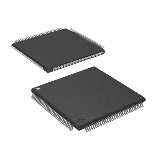


 工商网监
湘ICP备2023018690号
工商网监
湘ICP备2023018690号
