IXD1209/12
High Speed LDO Regulator with ON/OFF Control
FEATURES
o
o
o
o
o
o
o
o
o
o
o
o
DESCRIPTION
Output Current up to 150 mA (300 mA for
IXD2109E/H type)
Output Voltage Range from 0.9 V to 6.0 V with
0.05 V increments
Output Voltage Accuracy ±2% (at VOUT > 1.5 V),
± 30 mV (at VOUT ≤ 1.5 V)
Dropout Voltage 60 mV @ 30 mA , 0.20 V @
100 mA
Maximum Operating Voltage 10 V
Low Power Consumption at 25 µA typical
Standby Current less than 0.1 µA typical
Ripple Rejection 70 dB at 10 kHz
Low ESR Ceramic Capacitor compatible
0
Operating Ambient Temperature - 40 + 85 C
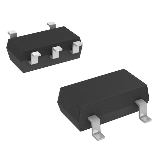
Packages : SOT-25, SOT-89-5 , and USP-6B
EU RoHS Compliant, Pb Free
The IXD1209/12 are a highly precise, low noise,
positive voltage LDO regulators manufactured using
CMOS processes. The IXD1209/12 have a high
ripple rejection factor and low dropout. They consist
of a voltage reference, an error amplifier, a current
limiter, a phase compensation circuit, and a driver
transistor.
Output voltage is selectable in 0.05V increments
within a range of 0.9 V ~ 6.0 V.
The IXD1209/12 are compatible with low ESR
ceramic capacitors, and due excellent transient
response, they maintain stability even during
significant load fluctuations. The current limiter's
foldback circuit operates also as a short circuit
protection.
The chip enable (CE) function allows disable IC,
greatly reducing power consumption.
Regulator is available in SOT-25, SOT-89-5, and
USP-6B packages.
APPLICATIONS
o
o
o
o
Mobile phones
Cameras, VCRs
Various portable equipment
Reference voltage source
TYPICAL APPLICATION CIRCUIT
TYPICAL PERFORMANCE CHARACTERISTIC
Supply Current vs. Input Voltage (IXD1209/12 F122)
© 2014 IXYS Corp.
Characteristics subject to change without notice
1
Doc. No. IXD1209/12_DS, Rev. N0
�IXD1209/12
ABSOLUTE MAXIMUM RATINGS
SYMBOL
RATINGS
Input Voltage
PARAMETER
VIN
– 0.3 ~ 12.0
V
Output Current
IOUT
5001)
mA
Output Voltage
VOUT
– 0.3 ~ VIN + 0.3
V
– 0.3 ~ 12.0
V
CE Input Voltage
VCE
SOT-25
Power Dissipation2)
UNITS
250 (600 PCB mounted)
SOT-89-5
PD
USP-6C
500 (1300 PCB mounted)
mW
120 (1000 PCB mounted)
Operating Temperature Range
TOPR
– 40 ~ + 85
0
Storage Temperature Range
TSTG
– 55 ~ +125
0
C
C
All voltages are in respect to VSS
1) IOUT ≤ Pd/ (VIN-VOUT)
2)This is a reference data taken by using the test board. Please refer to page 21 to 23 for details.
ELECTRICAL OPERATING CHARACTERISTICS
IXD1209/12 Type A, B
PARAMETER
Ta = 25 0C
SYMBOL
CONDITIONS
Output Voltage (2%)3)
Output Voltage (1%)4)
Maximum Output Current
Load Regulation
Dropout Voltage2)
Type A
Type B
Standby Current
VOUT(E)1)
IOUT = 30 mA
IOUT_MAX
∆VOUT
VDIF1
VDF2
VIN = 2.3 V, VOUT ≥ 1.17 V
1 mA ≤ IOUT ≤ 100 mA
IOUT = 30 mA
IOUT = 100mA
ISS
VCE = VIN = VOUT(E) + 1.0 V
When VOUT ≤ 0.95 V, VCE = VIN = 2.0 V
Supply
Current
ISTB
∆
Line Regulation
∆
Input Voltage
Output Voltage Temperature
Characteristics
∆
Power Supply Rejection Ratio
PSRR
Current Limit
ILIM
Short Current
ISHORT
CE “H” Level Voltage
CE “L” Level Voltage
Type A
CE “H” Level
Current
Type B
CE “L” Level Current
VCE = 0 V
VOUT(E) + 1.0 V ≤ VIN ≤ 10 V
When VOUT ≤ 0.95 V, 2.0 V ≤ VIN ≤ 10 V
IOUT = 30 mA,
When VOUT ≤ 1.75 V, IOUT = 10 mA
VIN
∆
ICEL
TYP.
MAX.
UNIT
VOUT(T)*
VOUT(T)x
1.02
VOUT(T)x
1.01
V
VOUT(T)*
55
50
0.10
0.01
0.20
%/V
10
V
mV
µA
µA
± 100
ppm/0C
70
dB
300
mA
50
1.6
VCE = VIN = VOUT(E) + 1.0 V
When VOUT ≤ 0.95 V, VCE = VIN = 2.0 V
VCE = 0 V, VIN = VOUT(E) + 1.0 V
When VOUT ≤ 0.95 V, VCE = VIN = 2.0 V
50
CIRCUIT
mA
mV
15
E-1
E-2
28
25
0.01
2
IOUT = 30 mA
- 40 0C ≤ TOPR ≤ 85 0C
VIN = (VOUT(E) + 1.0 V) + 1 Vp-pAC
When VOUT ≤ 1.5 V,
VIN = 2.5 V + 1.0 Vp-pAC,
IOUT = 10 mA, f = 10 kHz
VIN = VOUT(E) + 1.0 V, VCE = 0 V
When VOUT ≤ 1.75 V, VIN = VOUT(E) + 2.0 V
VCE = 0 V, When VOUT ≤ 1.75 V,
VIN = VOUT(E) + 2.0 V
VCEH
VCEL
ICEH
MIN.
VOUT(T)x
0.98
VOUT(T)x
0.99
60
mA
0.8
-0.1
VIN
0.25
5.0
0.1
-0.1
0.1
V
V
µA
µA
NOTE:
1)
2)
3)
4)
Unless otherwise stated, VIN = VOUT (T) +1.0 V. If VOUT is less than 0.95 V, VIN = 2.0 V; VOUT (T) is Nominal output voltage and VOUT (E) is
Effective output voltage, (I.e. the output voltage when "VOUT (T) +1.0V" is provided at the VIN pin, while maintaining a certain IOUT value).
VDIF = {VIN-VOUT}, where VIN1 is the input voltage when VOUT = 0.98 VOUT(T) appears, while input voltage gradually decreases
If VOUT (T) is less than 1.45 V, MIN. = VOUT (T) - 30 mV, MAX. = VOUT(T) + 30 mV
For products with VOUT(T) > 3.0 V only
© 2014 IXYS Corp.
Characteristics subject to change without notice
2
Doc. No. IXD1209/12_DS, Rev. N0
�IXD1209/12
ELECTRICAL OPERATING CHARACTERISTICS (CONTINUED)
IXD1209/12 Type C, D
PARAMETER
Ta = 25 0C
SYMBOL
CONDITIONS
Output Voltage (2%)3)
Output Voltage (1%)4)
Maximum Output Current
Load Regulation
Dropout Voltage2)
Type C
Type D
Standby Current
VOUT(E)1)
IOUT = 30 mA
IOUT_MAX
∆VOUT1
VDIF1
VDF2
VIN = 2.3 V, VOUT ≥ 1.17 V
1 mA ≤ IOUT ≤ 100 mA
IOUT = 30 mA
IOUT = 100mA
ISS
VCE = VIN = VOUT(E) + 1.0 V
When VOUT ≤ 0.95 V, VCE = VIN = 2.0 V
Supply
Current
ISTB
∆
Line Regulation
∆
Input Voltage
Output Voltage Temperature
Characteristics
∆
Power Supply Rejection Ratio
PSRR
Current Limit
ILIM
Short Current
ISHORT
CE “H” Level Voltage
CE “L” Level Voltage
VCEH
VCEL
CE “H” Level Current
ICEH
CE “L” Level
Current
Type C
Type D
VCE = 0 V
VOUT(E) + 1.0 V ≤ VIN ≤ 10 V
When VOUT ≤ 0.95 V, 2.0 V ≤ VIN ≤ 10 V
IOUT = 30 mA,
When VOUT ≤ 1.75 V, IOUT = 10 mA
VIN
∆
ICEL
MIN.
VOUT(T)x
0.98
VOUT(T)x
0.99
150
TYP.
MAX.
UNIT
VOUT(T)*
VOUT(T)x
1.02
VOUT(T)x
1.01
V
VOUT(T)*
VCE = VIN = VOUT(E) + 1.0 V
When VOUT ≤ 0.95 V, VCE = VIN = 2.0 V
VCE = 0 V, VIN = VOUT(E) + 1.0 V
When VOUT ≤ 0.95 V, VCE = VIN = 2.0 V
mA
mV
15
E-1
E-2
28
25
0.01
55
50
0.10
0.01
0.20
%/V
10
V
2
IOUT = 30 mA
- 40 0C ≤ TOPR ≤ 85 0C
VIN = (VOUT(E) + 1.0 V) + 1 Vp-pAC
When VOUT ≤ 1.5 V,
VIN = 2.5 V + 1.0 Vp-pAC,
IOUT = 10 mA, f = 10 kHz
VIN = VOUT(E) + 1.0 V, VCE = 0 V
When VOUT ≤ 1.75 V, VIN = VOUT(E) + 2.0 V
VCE = 0 V, When VOUT ≤ 1.75 V,
VIN = VOUT(E) + 2.0 V
50
CIRCUIT
mV
µA
µA
± 100
ppm/0C
70
dB
300
mA
50
mA
1.6
VIN
0.25
V
V
-0.1
0.1
µA
-5.0
-0.1
-0.8
0.1
µA
NOTE:
1)
2)
3)
4)
Unless otherwise stated, VIN = VOUT (T) +1.0 V. If VOUT is less than 0.95 V, VIN = 2.0 V; VOUT (T) is Nominal output voltage and VOUT (E) is
Effective output voltage, (I.e. the output voltage when "VOUT (T) +1.0V" is provided at the VIN pin, while maintaining a certain IOUT value).
VDIF = {VIN-VOUT}, where VIN1 is the input voltage when VOUT = 0.98 VOUT(T) appears, while input voltage gradually decreases
If VOUT (T) is less than 1.45 V, MIN. = VOUT (T) - 30 mV, MAX. = VOUT(T) + 30 mV
For products with VOUT (T) > 3.0 V only.
© 2014 IXYS Corp.
Characteristics subject to change without notice
3
Doc. No. IXD1209/12_DS, Rev. N0
�IXD1209/12
ELECTRICAL OPERATING CHARACTERISTICS (CONTINUED)
IXD1209/12 Type E, F
PARAMETER
Ta = 25 0C
SYMBOL
CONDITIONS
Output Voltage (2%)3)
Output Voltage (1%)4)
Maximum Output Current
Load Regulation
Dropout Voltage2)
Type G
Type H
Standby Current
VOUT(E)1)
IOUT = 30 mA
IOUT_MAX
∆VOUT1
∆VOUT2
VDIF1
VDF2
VIN = E-35)
1 mA ≤ IOUT ≤ 100 mA
1 mA ≤ IOUT ≤ 300 mA
IOUT = 30 mA
IOUT = 100mA
ISS
VCE = VIN = VOUT(E) + 1.0 V
When VOUT ≤ 0.95 V, VCE = VIN = 2.0 V
Supply
Current
ISTB
∆
Line Regulation
∆
Input Voltage
Output Voltage Temperature
Characteristics
∆
Power Supply Rejection Ratio
PSRR
Current Limit
ILIM
Short Current
ISHORT
CE “H” Level Voltage
CE “L” Level Voltage
Type E
CE “H” Level
Current
Type F
CE “L” Level Current
ICEL
MAX.
UNIT
VOUT(T)*
VOUT(T)x
1.02
VOUT(T)x
1.01
V
VOUT(T)*
VCE = VIN = VOUT(E) + 1.0 V
When VOUT ≤ 0.95 V, VCE = VIN = 2.0 V
VCE = 0 V, VIN = VOUT(E) + 1.0 V
When VOUT ≤ 0.95 V, VCE = VIN = 2.0 V
50
100
mV
E-1
E-2
28
25
0.01
55
50
0.10
0.01
0.20
%/V
10
V
mV
µA
µA
± 100
ppm/0C
70
dB
380
mA
50
1.6
CIRCUIT
mA
2
IOUT = 30 mA
- 40 0C ≤ TOPR ≤ 85 0C
VIN = (VOUT(E) + 1.0 V) + 1 Vp-pAC
When VOUT ≤ 1.5 V,
VIN = 2.5 V + 1.0 Vp-pAC,
IOUT = 10 mA, f = 10 kHz
VIN = VOUT(E) + 1.0 V, VCE = 0 V
When VOUT ≤ 1.75 V, VIN = VOUT(E) + 2.0 V
VCE = 0 V, When VOUT ≤ 1.75 V,
VIN = VOUT(E) + 2.0 V
VCEH
VCEL
ICEH
TYP.
15
VCE = 0 V
VOUT(E) + 1.0 V ≤ VIN ≤ 10 V
When VOUT ≤ 0.95 V, 2.0 V ≤ VIN ≤ 10 V
IOUT = 30 mA,
When VOUT ≤ 1.75 V, IOUT = 10 mA
VIN
∆
MIN.
VOUT(T)x
0.98
VOUT(T)x
0.99
E-4
mA
0.8
-0.1
VIN
0.25
5.0
0.1
-0.1
0.1
V
V
µA
µA
NOTE:
1)
2)
3)
4)
5)
Unless otherwise stated, VIN = VOUT (T) +1.0 V. If VOUT is less than 0.95 V, VIN = 2.0 V; VOUT (T) is Nominal output voltage and VOUT (E) is
Effective output voltage, (I.e. the output voltage when "VOUT (T) +1.0V" is provided at the VIN pin, while maintaining a certain IOUT value).
VDIF = {VIN-VOUT}, where VIN1 is the input voltage when VOUT = 0.98 VOUT(T) appears, while input voltage gradually decreases
If VOUT (T) is less than 1.45 V, MIN. = VOUT (T) - 30 mV, MAX. = VOUT(T) + 30 mV
For products with VOUT(T) > 3.0 V only
Refer to the “Dropout Voltage” table
© 2014 IXYS Corp.
Characteristics subject to change without notice
4
Doc. No. IXD1209/12_DS, Rev. N0
�IXD1209/12
ELECTRICAL OPERATING CHARACTERISTICS (CONTINUED)
IXD1209/12 Type G, H
PARAMETER
Ta = 25 0C
SYMBOL
CONDITIONS
Output Voltage (2%)3)
Output Voltage (1%)4)
Maximum Output Current
Load Regulation
Dropout Voltage2)
Type G
Type H
Standby Current
VOUT(E)1)
IOUT = 30 mA
IOUT_MAX
∆VOUT1
∆VOUT2
VDIF1
VDF2
VIN = E-35)
1 mA ≤ IOUT ≤ 100 mA
1 mA ≤ IOUT ≤ 300 mA
IOUT = 30 mA
IOUT = 100mA
ISS
VCE = VIN = VOUT(E) + 1.0 V
When VOUT ≤ 0.95 V, VCE = VIN = 2.0 V
Supply
Current
ISTB
∆
Line Regulation
∆
Input Voltage
Output Voltage Temperature
Characteristics
∆
Power Supply Rejection Ratio
PSRR
Current Limit
ILIM
Short Current
ISHORT
CE “H” Level Voltage
CE “L” Level Voltage
VCEH
VCEL
CE “H” Level Current
ICEH
CE “L” Level
Current
Type G
Type H
ICEL
TYP.
MAX.
UNIT
VOUT(T)*
VOUT(T)x
1.02
VOUT(T)x
1.01
V
VOUT(T)*
VCE = VIN = VOUT(E) + 1.0 V
When VOUT ≤ 0.95 V, VCE = VIN = 2.0 V
VCE = 0 V, VIN = VOUT(E) + 1.0 V
When VOUT ≤ 0.95 V, VCE = VIN = 2.0 V
50
100
mV
E-1
E-2
28
25
0.01
55
50
0.10
0.01
0.20
%/V
10
V
2
IOUT = 30 mA
- 40 0C ≤ TOPR ≤ 85 0C
VIN = (VOUT(E) + 1.0 V) + 1 Vp-pAC
When VOUT ≤ 1.5 V,
VIN = 2.5 V + 1.0 Vp-pAC,
IOUT = 10 mA, f = 10 kHz
VIN = VOUT(E) + 1.0 V, VCE = 0 V
When VOUT ≤ 1.75 V, VIN = VOUT(E) + 2.0 V
VCE = 0 V, When VOUT ≤ 1.75 V,
VIN = VOUT(E) + 2.0 V
CIRCUIT
mA
15
VCE = 0 V
VOUT(E) + 1.0 V ≤ VIN ≤ 10 V
When VOUT ≤ 0.95 V, 2.0 V ≤ VIN ≤ 10 V
IOUT = 30 mA,
When VOUT ≤ 1.75 V, IOUT = 10 mA
VIN
∆
MIN.
VOUT(T)x
0.98
VOUT(T)x
0.99
E-4
mV
µA
µA
± 100
ppm/0C
70
dB
380
mA
50
mA
1.6
VIN
0.25
V
V
-0.1
0.1
µA
-5.0
-0.1
-0.8
0.1
µA
NOTE:
1)
2)
3)
4)
5)
Unless otherwise stated, VIN = VOUT (T) +1.0 V. If VOUT is less than 0.95 V, VIN = 2.0 V; VOUT (T) is Nominal output voltage and VOUT (E) is
Effective output voltage, (I.e. the output voltage when "VOUT (T) +1.0V" is provided at the VIN pin, while maintaining a certain IOUT value).
VDIF = {VIN-VOUT}, where VIN1 is the input voltage when VOUT = 0.98 VOUT(T) appears, while input voltage gradually decreases
If VOUT (T) is less than 1.45 V, MIN. = VOUT (T) - 30 mV, MAX. = VOUT(T) + 30 mV
For products with VOUT (T) > 3.0 V only.
Refer to the “Dropout Voltage” table
© 2014 IXYS Corp.
Characteristics subject to change without notice
5
Doc. No. IXD1209/12_DS, Rev. N0
�IXD1209/12
ELECTRICAL OPERATING CHARACTERISTICS (CONTINUED)
Dropout Voltage for products with ± 2% accuracy
SYMBOL
E-0
NOMINAL
VOLTAGE
OUTPUT VOLTAGE, V (± 2%)
VOUT(T)
0.90
0.95
1.00
1.05*
1.10*
1.15*
1.20*
1.25*
1.30*
1.35*
1.40*
1.45*
1.50*
1.55*
1.60*
1.65*
1.70*
1.75*
1.80*
1.85*
1.90*
1.95*
2.00
2.05
2.10
2.15
2.20
2.25
2.30
2.35
2.40
2.45
2.50
2.55
2.60
2.65
2.70
2.75
2.80
2.85
2.90
2.95
3.00
3.05
3.10
3.15
3.20
3.25
3.30
3.35
3.40
3.45
3.50
3.55
VOUT
MIN.
0.870
0.920
0.970
1.020
1.070
1.120
1.170
1.220
1.270
1.320
1.370
1.420
1.470
1.519
1.568
1.617
1.666
1.715
1.764
1.813
1.862
1.911
1.960
2.009
2.058
2.107
2.156
2.205
2.254
2.303
2.352
2.401
2.450
2.499
2.548
2.597
2.646
2695
2.744
2.793
2.842
2.891
2.940
2.989
3.038
3.087
3.136
3.185
3.234
3.283
3.332
3.381
3.430
3.479
MAX.
0.930
0.980
1.030
1.080
1.130
1.180
1.230
1.280
1.330
1.380
1.430
1.480
1.530
1.581
1.632
1.683
1.734
1.785
1.836
1.887
1.938
1.989
2.040
2.091
2.142
2.193
2.244
2.295
2.346
2.397
2.448
2.499
2.550
2.601
2.652
2.703
2.754
2.805
2.856
2.907
2.958
3.009
3.060
3.111
3.162
3.213
3.264
3.315
3.366
3.417
3.468
3.519
3.570
3.621
E-1
DROPOUT VOLTAGE1, mV
IOUT = 30 mA
VDIF1
TYP.
MAX.
E-2
DROPOUT VOLTAGE 2, mV
IOUT = 100 mA
VDIF2
TYP.
MAX.
1100
1110
1150
1200
1000
1010
1050
1100
900
910
950
1000
800
810
850
900
700
710
750
800
600
610
650
700
500
510
550
600
400
410
500
550
300
310
400
450
200
210
300
400
120
150
280
380
350
330
80
120
240
310
290
70
100
220
270
60
90
200
250
* Required operating voltage is VIN ≥ 2.0 V minimum. VDIF = 2.0 V-VOUT (T) minimum
© 2014 IXYS Corp.
Characteristics subject to change without notice
6
Doc. No. IXD1209/12_DS, Rev. N0
�IXD1209/12
ELECTRICAL OPERATING CHARACTERISTICS (CONTINUED)
Dropout Voltage for products with ± 2% accuracy
SYMBOL
E-0
NOMINAL
VOLTAGE
OUTPUT VOLTAGE, V (± 2%)
VOUT(T)
3.60
3.65
3.70
3.75
3.80
3.85
3.90
3.95
4.00
4.05
4.10
4.15
4.20
4.25
4.30
4.35
4.40
4.45
4.50
4.55
4.60
4.65
4.70
4.75
4.80
4.85
4.90
4.95
5.00
5.05
5.10
5.15
5.20
5.25
5.30
5.35
5.40
5.45
5.50
5.55
5.60
5.65
5.70
5.75
5.80
5.85
5.90
5.95
6.00
VOUT
MIN.
3.528
3.577
3.626
3.675
3.724
3.773
3.822
3.871
3.920
3.969
4.018
4.067
4.116
4.165
4.214
4.263
4.312
4.361
4.410
4.459
4.508
4.557
4.606
4.655
4.704
4.753
4.802
4.851
4.900
4.949
4.998
5.047
5.096
5.145
5.194
5.243
5.292
5.341
5.390
5.439
5.488
5.537
5.586
5.635
5.684
5.733
5.782
5.831
5.880
MAX.
3.672
3.723
3.774
3.825
3.876
3.927
3.978
4.029
4.080
4.131
4.182
4.233
4.284
4.335
4.386
4.437
4.488
4.539
4.590
4.641
4.692
4.743
4.794
4.845
4.896
4.947
4.998
5.049
5.100
5.151
5.202
5.253
5.304
5.355
5.406
5.457
5.508
5.559
5.610
5.661
5.712
5.763
5.814
5.865
5.916
5.967
6.018
6.069
6.120
© 2014 IXYS Corp.
Characteristics subject to change without notice
E-1
DROPOUT VOLTAGE1, mV
IOUT = 30 mA
VDIF1
TYP.
MAX.
E-2
DROPOUT VOLTAGE 2, mV
IOUT = 100 mA
VDIF2
TYP.
MAX.
90
200
250
80
180
230
70
160
210
60
50
7
Doc. No. IXD1209/12_DS, Rev. N0
�IXD1209/12
ELECTRICAL OPERATING CHARACTERISTICS (CONTINUED)
Output Voltage for products with ± 1% accuracy
SYMBOL
VOUT(T)
3.00
3.05
3.10
3.15
3.20
3.25
3.30
3.35
3.40
3.45
3.50
3.55
3.60
3.65
3.70
3.75
3.80
3.85
3.90
3.95
4.00
4.05
4.10
4.15
4.20
4.25
4.30
4.35
4.40
4.45
4.50
E-0
OUTPUT VOLTAGE, V (1%)
VOUT
MIN.
MAX.
2.970
3.030
3.020
3.081
3.069
3.131
3.119
3.182
3.168
3.232
3.218
3.283
3.267
3.333
3.317
3.384
3.366
3.434
3.416
3.485
3.465
3.535
3.515
3.586
3.564
3.636
3.614
3.687
3.663
3.737
3.713
3.788
3.762
3.838
3.812
3.889
3.861
3.939
3.911
3.990
3.960
4.040
4.010
4.091
4.059
4.141
4.109
4.192
4.158
4.242
4.208
4.293
4.257
4.343
4.307
4.394
4.356
4.444
4.405
4.494
4.455
4.545
SYMBOL
VOUT(T)
4.55
4.60
4.65
4.70
4.75
4.80
4.85
4.90
4.95
5.00
5.05
5.10
5.15
5.20
5.25
5.30
5.35
5.40
5.45
5.50
5.55
5.60
5.65
5.70
5.75
5.80
5.85
5.90
5.95
6.00
E-0
OUTPUT VOLTAGE, V (1%)
VOUT
MIN.
MAX.
4.505
4.596
4.554
4.646
4.604
4.697
4.653
4.747
4.703
4.798
4.752
4.848
4.802
4.899
4.851
4.949
4.901
5.000
4.950
5.050
4.000
5.101
4.049
5.151
4.099
5.202
4.148
5.252
5.198
5.303
5.247
5.353
5.297
5.404
5.346
5.454
5.396
5.505
5.445
5.555
5.495
5.606
5.544
5.656
5.594
5.707
5.643
5.757
5.963
5.808
5.742
5.858
5.792
5.909
5.841
5.959
5.891
6.010
5.940
6.060
Conditions
SYMBOL
NOMINAL OUTPUT VOLTAGE, V
VOUT(T)
0.90 ~ 0.95
1.00 ~ 1.05
1.10 ~ 1.15
1.20 ~ 1.25
1.30 ~ 1.35
1.40 ~ 1.45
1.50 ~ 1.95
2.00 ~ 6.00
E-3
INPUT VOLTAGE, V
VIN
2.5
2.5
2.6
2.7
2.8
2.9
3.0
VOUT(T) + 1.0
© 2014 IXYS Corp.
Characteristics subject to change without notice
E-4
MAXIMUM OUTPUT CURRENT, (mA)
MIN VALUE
260
260
270
290
300
8
Doc. No. IXD1209/12_DS, Rev. N0
�IXD1209/12
PIN CONFIGURATION
IXD1209
*The dissipation pad for the USP-6B
package should be solder-plated in
recommended mounting pattern and
metal masking to enhance mounting
strength and heat release.
If the pad needs to be connected to
other pins, it should be connected to the
VSS (No.5) pin.
IXD1212
PIN ASSIGNMENT
SOT-25
1
2
3
4
5
PIN NUMBER
IXD1209
USP-6B
SOT-89 5
4
1
2
5
3
6
1
2, 4
5
3
IXD1212
SOT-25
3
2
4
5
1
PIN NAME
VIN
VSS
CE
NC
VOUT
FUNCTIONS
Power Input
Ground
ON/OFF Control
No Connection
Output Voltage
CE PIN FUNCTION
IC TYPE
CE PIN STATE
IC STATE
H
L
H
L
ON
OFF
OFF
ON
A, B, E, F
C, D, G, H
BLOCK DIAGRAMS
IXD2109/12 Type A, E
IXD2109/12 Type B, D, F, H
Diodes inside the circuits are ESD protection diodes and parasitic diodes.
© 2014 IXYS Corp.
Characteristics subject to change without notice
9
IXD2109/12 Type C, G
Doc. No. IXD1209/12_DS, Rev. N0
�IXD1209/12
BASIC OPERATION
The Error Amplifier of the IXD1209/12 series monitors output voltage divided by internal resistors R1 & R2 and
compares it with the internal Reference Voltage (see Block Diagram above). The output signal from error amplifier
drives gate of the P-channel MOSFET, which is connected to the VOUT pin and operates as a series voltage
regulator.
The Current Limit and Short Protection circuits monitor level of the output current. The CE pin allows shutdown
internal circuitry to minimize power consumption.
Low ESR Capacitors
An internal phase compensation circuit guarantees stable IXD1209/12 operation even if output capacitors with low
ESR are used. However, connect the output capacitor CL as close to the VOUT and the VSS pins as possible to
prevent effectiveness of the phase compensation from degrade. The CL capacitance value should be at least 1µF.
In case the capacitor depends on the bias and temperature, make sure that actual capacitance is maintained at
operating voltage and temperature range. In addition, an input capacitor CIN ≥ 0.1µF between the VIN and VSS pins
should be used to ensure a stable input power.
Current Limiter, Short-Circuit Protection
The IXD1209/12 series include a combination of a fixed current limiter circuit & a foldback circuit, which aid the
operations of the current limiter and circuit protection. When the load current reaches the current limit level, the
fixed current limiter circuit activates and output voltage drops. Because of this drop, the foldback circuit activates
too, and output voltage drops further decreasing output current. When the output pin is shorted, a current of about
50 mA flows.
CE Pin
The CE pin allows shutdown internal circuitry to minimize power consumption. In shutdown mode, output at the
VOUT pin is pulled down to the VSS level via R1 & R2. The operational logic of the CE pin is selectable (please, refer
to the CE PIN FUNCTION Table above).
Note that the standard IXD1209/12B type CE input is an Active High/No Pull Down and operations will become
unstable, if the CE pin is open. CE pin should be used with either VIN or VSS voltage. If this IC is used with some
intermediate voltage at CE pin, supply current may increase due through current in the IC's internal circuitry.
TYPICAL APPLICATION CIRCUIT
The output capacitor CL ≥ 1 µF should be connected between the output pin (VOUT) and the VSS pin for stable regulator’s operation.
Ceramic capacitors with low ESR are recommended.
LAYOUT AND USE CONSIDERATIONS
1. Mount external component as close to the IC as possible and use thick, short connecting traces to
reduce the circuit impedance.
2. The IC may malfunction if absolute maximum ratings are exceeded.
3. If power source of this regulator is a high impedance device with impedance of 10 Ω or more, an input
capacitor CIN ≥ 1µF should be used to prevent oscillations.
4. In case of high output current, increasing the input capacitor value can stabilize operations.
5. Oscillations may occur also, if the input capacitor value is not enough to reduce the input impedance
and the output capacitor CL is large. In such case, operations can be stabilized by either increasing the
input capacitor or reducing the output capacitor.
6. During start-up, IC provides constant current until VOUT = VOUT (T).
7. Please ensure that output current IOUT is less than PD / (VIN - VOUT), where PD is a rated power
dissipation value of the package shown at ABSOLUTE MAXIMUM RATING table to not exceed it.
© 2014 IXYS Corp.
Characteristics subject to change without notice
10
Doc. No. IXD1209/12_DS, Rev. N0
�IXD1209/12
TEST CIRCUITS
Circuit
Circuit
Circuit
Circuit
VIN = VOUT + 1.0 VDC + 1.0 Vp-pAC, if VOUT ≤ 1.5 V, VIN = 2.5 VDC + 1.0 Vp-pAC
* Each Test Circuit, VCE (CE pin Voltage)
IC Active State
IXD1209/12, Type A, B, E, F: VCE=VIN
IXD1209/12, Type C, D, G, H: VCE=VSS
IC in Standby mode
IXD1209/12, Type A, B, E, F: VCE=VSS
IXD1209/12, Type C, D, G, H: VCE=VIN
TYPICAL PERFORMANCE CHARACTERISTICS
(1) Ripple rejection Ratio
IXD1209/12 BF302
IXD1209/12 B/F122
VIN = 4 VDC + 1 Vp-pAC, IOUT = 30 mA, CL = 1 µF (ceramic)
VIN = 2.5 VDC + 1 Vp-pAC, IOUT = 30 mA, CL = 1 µF (ceramic)
© 2014 IXYS Corp.
Characteristics subject to change without notice
11
Doc. No. IXD1209/12_DS, Rev. N0
�IXD1209/12
TYPICAL PERFORMANCE CHARACTERISTICS (Continued)
(2) Output Voltage vsOutput Current
Topr = 25 0C
IXD1209/12 B302
IXD1209/12 B302
CIN = CL = 1µF, (ceramic), VIN = 4.0 V
CIN = CL = 1µF, (ceramic), Ta = 250C
IXD1209/12 F302
IXD1209/12 F302
CIN = CL = 1µF, (ceramic), VIN = 4.0 V
CIN = CL = 1µF, (ceramic), Ta = 250C
IXD1209/12 B122
IXD1209/12 B122
CIN = CL = 1µF, (ceramic), VIN = 2.7 V
CIN = CL = 1µF, (ceramic), Ta = 250C
© 2014 IXYS Corp.
Characteristics subject to change without notice
12
Doc. No. IXD1209/12_DS, Rev. N0
�IXD1209/12
TYPICAL PERFORMANCE CHARACTERISTICS (Continued)
(2) Output Voltage vs. Output Current (Continue)
Topr = 25 0C
IXD1209/12 F122
IXD1209/12 F122
CIN = CL = 1µF, (ceramic), VIN = 2.7 V
CIN = CL = 1µF, (ceramic), Ta = 25 C
0
(3) Output Voltage vs. Input Voltage
IXD1209/12 F302
IXD1209/12 F302
CIN = CL = 1µF, (ceramic), Ta = 250C
CIN = CL = 1µF, (ceramic), Ta = 250C
IXD1209/12 F302
IXD1209/12 F302
0
0
CIN = CL = 1µF, (ceramic), Ta = 25 C
© 2014 IXYS Corp.
Characteristics subject to change without notice
CIN = CL = 1µF, (ceramic), Ta = 25 C
13
Doc. No. IXD1209/12_DS, Rev. N0
�IXD1209/12
TYPICAL PERFORMANCE CHARACTERISTICS (Continued)
(4) Dropout Voltage vs. Output Current
Topr = 25 0C
IXD1209/12 B302
IXD1209/12 F302
CIN = CL = 1µF, (ceramic)
CIN = CL = 1µF, (ceramic)
IXD1209/12 B122
IXD1209/12 F122
CIN = CL = 1µF, (ceramic)
CIN = CL = 1µF, (ceramic)
(5) Supply Current vs. Input Voltage
IXD1209/12 F302
© 2014 IXYS Corp.
Characteristics subject to change without notice
IXD1209/12 F122
14
Doc. No. IXD1209/12_DS, Rev. N0
�IXD1209/12
TYPICAL PERFORMANCE CHARACTERISTICS (Continued)
(6) Output Voltage vs. Ambient temperasture
IXD1209/12 B/F302
IXD1209/12 B122
CIN = CL = 1µF, (ceramic), VIN = 4.0 V
CIN = CL = 1µF, (ceramic), VIN = 2.5 V
(7) Supply Current vs. Ambient temperature
IXD1209/12 B/F302
IXD1209/12 B122
VIN = 4.0 V
VIN = 2.5 V
IXD1209
(8) P-channel Transistor Characteristics
IXD1209/12 B/F
0
Ta = 25 C
© 2014 IXYS Corp.
Characteristics subject to change without notice
15
Doc. No. IXD1209/12_DS, Rev. N0
�IXD1209/12
TYPICAL PERFORMANCE CHARACTERISTICS (Continued)
(9) Input Voltage Transient Response
IXD1209/12 B/F302
IXD1209/12 B/F302
CIN = CL = 1µF, (ceramic), IOUT = 1 mA, tR = 5 us
CIN = CL = 1µF, (ceramic), IOUT = 30 mA, tR = 5 us
IXD1209/12 B/F302
IXD1209/12 B122
CIN = CL = 1µF, (ceramic), IOUT = 100 mA, tR = 5 us
CIN = CL = 1µF, (ceramic), IOUT = 1 mA, tR = 5 us
IXD1209/12 B122
IXD1209/12 B122
CIN = CL = 1µF, (ceramic), IOUT = 30 mA, tR = 5 us
CIN = CL = 1µF, (ceramic), IOUT = 100 mA, tR = 5 us
© 2014 IXYS Corp.
Characteristics subject to change without notice
16
Doc. No. IXD1209/12_DS, Rev. N0
�IXD1209/12
TYPICAL PERFORMANCE CHARACTERISTICS (Continued)
(10) Load Transient Response
IXD1209/12 B/F302
IXD1209/12 B/F302
CIN = CL = 1µF, (ceramic), VIN = 4.0 V, tR = tF = 5 us
CIN = 1µF, (ceramic), CL = 2.2 µF, (ceramic), VIN = 4.0 V, tR = tF = 5 us
IXD1209/12 B/F302
IXD1209/12 B/F302
CIN = CL = 1µF, (ceramic), VIN = 4.0 V, tR = tF = 5 us
CIN = 1µF, (ceramic), CL = 2.2 µF, (ceramic), VIN = 4.0 V, tR = tF = 5 us
IXD1209/12 B/F302
IXD1209/12 B/F302
CIN = CL = 1µF, (ceramic), VIN = 4.0 V, tR = tF = 5 us
CIN = 1µF, (ceramic), CL = 2.2 µF, (ceramic), VIN = 4.0 V, tR = tF = 5 us
© 2014 IXYS Corp.
Characteristics subject to change without notice
17
Doc. No. IXD1209/12_DS, Rev. N0
�IXD1209/12
TYPICAL PERFORMANCE CHARACTERISTICS (Continued)
(10) Load Transient Response (Continued)
IXD1209/12 B/F122
IXD1209/12 B/F122
CIN = CL = 1µF, (ceramic), VIN = 2.5 V, tR = tF = 5 us
CIN = 1µF, (ceramic), CL = 2.2 µF, (ceramic), VIN = 2.5 V, tR = tF = 5 us
IXD1209/12 B/F122
IXD1209/12 B/F122
CIN = CL = 1µF, (ceramic), VIN = 2.5 V, tR = tF = 5 us
CIN = 1µF, (ceramic), CL = 2.2 µF, (ceramic), VIN = 2.5 V, tR = tF = 5 us
IXD1209/12 B/F122
IXD1209/12 B/F122
CIN = CL = 1µF, (ceramic), VIN = 2.5 V, tR = tF = 5 us
CIN = 1µF, (ceramic), CL = 2.2 µF, (ceramic), VIN = 2.5 V, tR = tF = 5 us
© 2014 IXYS Corp.
Characteristics subject to change without notice
18
Doc. No. IXD1209/12_DS, Rev. N0
�IXD1209/12
ORDERING INFORMATION
IXD1209
IXD1212
-
DESIGNATOR
DESCRIPTION
Type of Regulator
CE PIN Logic
Output Voltage
Output Voltage Accuracy
SYMBOL
A
B
C
D
E
F
G
H
09 - 60
30 - 60
-
Packages
(Order Limit)
150 mA, Active High, Pull-down resistor built-in (*2) (Semi-custom)
150 mA, Active High, No pull-down resistor (Standard)
150 mA, Active Low, Pull-up resistor built-in (*2) (Semi-custom)
150 mA, Active Low, No pull-up resistor (Semi-custom)
300 mA (*1), Active High, Pull-down resistor built-in (*2) (Semi-custom)
300 mA ( *1), Active High, No pull-down resistor (Standard)
300 mA (*1), Active Low, Pull-up resistor built-in (*2) (Semi-custom)
300 mA (*1), Active Low, No pull-up resistor (Semi-custom)
= 3,
=0
Output Voltage Range: 0.9 V~6.0 V, e.g. 3.0 V For 1% product, output voltage range is 3.0 V~6.0 V.
1
0.1 V increments, Accuracy: ±1%, e.g. 3.00 V -
2
0.1 V increments, Accuracy: ±2% (*3), e.g. 2.80V (*3)
A
0.05 V increments, Accuracy: ±2%
B
0.05 V increments, Accuracy: ±1%, e.g.: 3.05 V -
MR
(*4)
DESCRIPTION
= 3,
, e.g.: 2.85 V -
= 0,
= 2,
= 2,
= 3,
=1
= 8,
= 8,
= 0,
=2
=A
=B
SOT-25 (3000/Reel)
MR-G
SOT-25 (3000/Reel)
PR
SOT-89 (3000/Reel)
PR-G
SOT-89 (3000/Reel)
DR
USP-6B (3000/Reel)
DR-G
USP-6B (3000/Reel)
NOTE:
(*1) The maximum output current of type E ~ H depends on setting output voltage.
(*2) With the pull-up resistor or pull-down resistor built-in types, the supply current during operation will increase by VIN / 2 MΩ (TYP.).
(*3) The output voltage accuracy is ±30 mV at VOUT ≤ 1.5 V.
(*4) The “-G” suffix denotes Halogen and Antimony free as well as being fully RoHS compliant.
© 2014 IXYS Corp.
Characteristics subject to change without notice
19
Doc. No. IXD1209/12_DS, Rev. N0
�IXD1209/12
PACKAGE DRAWING AND DIMENSIONS
SOT-25, Units: mm
SOT-89-5, Units: mm
USP-6B, Units: mm
USP-6B Reference Pattern Layout, Units: mm
USP-6B Reference Metal Mask Design, Units: mm
© 2014 IXYS Corp.
Characteristics subject to change without notice
20
Doc. No. IXD1209/12_DS, Rev. N0
�IXD1209/12
PACKAGE POWER DISSIPATION
SOT-25 Power Dissipation
The power dissipation varies with the mount board conditions.
Please use this data as a reference only.
1. Measurement Conditions:
Condition:
Ambient:
Soldering:
Board:
Material:
Thickness:
Through-hole:
Mount on a board
Natural convection
Lead (Pb) free
Dimensions 40×40 mm (1600 mm2 in one side)
Copper (Cu) traces occupy 50% of the board area
on top and bottom layers
Package heat sink tied to the copper traces.
(Board of SOT-26 is used)
Glass Epoxy (FR-4)
1.6 mm
4 x 0.8 Diameter
2. Power Dissipation vs. Ambient Temperature
Board Mount (Tjmax = 125 0C)
Ambient
Temperature, 0C
Power Dissipation
Pd, mW
Thermal Resistance,
0
C/W
25
85
600
240
166.67
© 2014 IXYS Corp.
Characteristics subject to change without notice
21
Doc. No. IXD1209/12_DS, Rev. N0
�IXD1209/12
PACKAGE POWER DISSIPATION (CONTINUED)
SOT-89-5 Power Dissipation
The power dissipation varies with the mount board conditions.
Please use this data as a reference only.
1. Measurement Conditions:
Condition:
Ambient:
Soldering:
Board:
Material:
Thickness:
Through-hole:
Mount on a board
Natural convection
Lead (Pb) free
Dimensions 40×40 mm (1600 mm2 in one side)
Copper (Cu) traces occupy 50% of the board area
on top and bottom layers
Package heat sink tied to the copper traces.
(Board of SOT-26 is used)
Glass Epoxy (FR-4)
1.6 mm
5 x 0.8 Diameter
2. Power Dissipation vs. Ambient Temperature
Board Mount (Tjmax = 125 0C)
Ambient
Temperature, 0C
Power Dissipation
Pd, mW
Thermal Resistance,
0
C/W
25
85
1300
520
76.92
© 2014 IXYS Corp.
Characteristics subject to change without notice
22
Doc. No. IXD1209/12_DS, Rev. N0
�IXD1209/12
PACKAGE POWER DISSIPATION (CONTINUED)
USP-6B Power Dissipation
The power dissipation varies with the mount board conditions.
Please use this data as a reference only.
1. Measurement Conditions:
Condition:
Ambient:
Soldering:
Board:
Material:
Thickness:
Through-hole:
Mount on a board
Natural convection
Lead (Pb) free
Dimensions 40×40 mm (1600 mm2 in one side)
Copper (Cu) traces occupy 50% of the board area
on top and bottom layers
Package heat sink tied to the copper traces.
(Board of SOT-26 is used)
Glass Epoxy (FR-4)
1.6 mm
4 x 0.8 Diameter
2. Power Dissipation vs. Ambient Temperature
Board Mount (Tjmax = 125 0C)
Ambient
Temperature, 0C
Power Dissipation
Pd, mW
Thermal Resistance,
0
C/W
25
85
1000
400
100.00
© 2014 IXYS Corp.
Characteristics subject to change without notice
23
Doc. No. IXD1209/12_DS, Rev. N0
�IXD1209/12
MARKING
IXD1209
SOT-25, SOT 89
- represents product series
MARK
9
PRODUCT SERIES
IXD1209xxxxx
- represents type of regulator
MARK
VOUT 0.1 V INCREMENTS
VOUT 0.05 V INCREMENTS
PRODUCT SERIES
Voltage
0.1 – 3.0 V
Voltage
3.1 – 6.0 V
Voltage
0.15 – 3.05 V
V
A
E
L
IXD1209Axxxxx
X
B
F
M
IXD1209Bxxxxx
Y
C
H
N
IXD1209Cxxxxx
Z
D
K
P
IXD1209Dxxxxx
V
A
E
L
IXD1209Exxxxx
X
B
F
M
IXD1209Fxxxxx
Y
C
H
N
IXD1209Gxxxxx
Z
D
K
P
IXD1209Hxxxxx
③
Voltage
3.15 – 6.05 V
- represents output voltage
MARK
0
1
2
3
4
5
6
7
8
9
A
B
C
D
E
OUTPUT VOLTAGE, V
0.9
1.0
1.1
1.2
1.3
1.4
1.5
3.1
3.2
3.3
3.4
3.5
3.6
3.7
3.8
3.9
4.0
4.1
4.2
4.3
4.4
4.5
MARK
3.15
3.25
3.35
3.45
3.55
3.65
3.75
3.85
3.95
4.05
4.15
4.25
4.35
4.45
4.55
0.95
1.05
1.15
1.25
1.35
1.45
1.55
F
H
K
L
M
N
P
R
S
T
U
V
X
Y
Z
OUTPUT VOLTAGE, V
1.6
1.7
1.8
1.9
2.0
2.1
2.2
2.3
2.4
2.5
2.6
2.7
2.8
2.9
3.0
4.6
4.7
4.8
4.9
5.0
5.1
5.2
5.3
5.4
5.5
5.6
5.7
5.8
5.9
6.0
1.65
1.75
1.85
1.95
2.05
2.15
2.25
2.35
2.45
2.55
2.65
2.75
2.85
2.95
3.05
4.65
4.75
4.85
4.95
5.05
5.15
5.25
5.35
5.45
5.55
5.65
5.75
5.85
5.95
6.05
- represents production lot number 0 to 9, A to Z repeated (G, I, J, O, Q, W excluded)
© 2014 IXYS Corp.
Characteristics subject to change without notice
24
Doc. No. IXD1209/12_DS, Rev. N0
�IXD1209/12
MARKING (Continue)
IXD1209
USP-6B
- represents product series
MARK
0
PRODUCT SERIES
9
IXD1209xxxxDx
- represents type of regulator
MARK
A
B
C
D
TYPE
CE pin, Active High pull-down resistor built in
CE pin, Active High no pull-down resistor built in
CE pin, Active Low pull-up resistor built in
CE pin, Active Low no pull-up resistor built in
PRODUCT SERIES
IXD1209AxxxDx
IXD1209BxxxDx
IXD1209CxxxDx
IXD1209DxxxDx
- represents integer of the output voltage
MARK
VOLTAGE, V
PRODUCT SERIES
3
3.x
IXD1209x3xxDx
5
5.x
IXD1209x5xxDx
- represents decimal number of the output voltage
MARK
0
1
2
3
4
5
6
7
8
9
VOLTAGE, V
x.0
x.1
x.2
x.3
x.4
x.5
x.6
x.7
x.8
x.9
PRODUCT SERIES
IXD1209xx0xDx
IXD1209xx1xDx
IXD1209xx2xDx
IXD1209xx3xDx
IXD1209xx4xDx
IXD1209xx5xDx
IXD1209xx6xDx
IXD1209xx7xDx
IXD1209xx8xDx
IXD1209xx9xDx
MARK
A
B
C
D
E
F
H
K
L
M
VOLTAGE, V
x.05
x.15
x.25
x.35
x.45
x.55
x.65
x/75
x.85
x.95
PRODUCT SERIES
IXD1209xx0ADx
IXD1209xx1ADx
IXD1209xx2ADx
IXD1209xx3ADx
IXD1209xx4ADx
IXD1209xx5ADx
IXD1209xx6ADx
IXD1209xx7ADx
IXD1209xx8ADx
IXD1209xx9ADx
- represents production lot number 0 to 9, A to Z repeated (G, I, J, O, Q, W excluded
© 2014 IXYS Corp.
Characteristics subject to change without notice
25
Doc. No. IXD1209/12_DS, Rev. N0
�IXD1209/12
MARKING
IXD1212
SOT-25
- represents product series
MARK
9
PRODUCT SERIES
IXD1212xxxMx
- represents type of regulator
MARK
VOUT 0.1 V INCREMENTS
VOUT 0.05 V INCREMENTS
PRODUCT SERIES
Voltage
0.1 – 3.0 V
Voltage
3.1 – 6.0 V
Voltage
0.15 – 3.05 V
V
A
E
L
IXD1212AxxxMx
X
B
F
M
IXD1212BxxxMx
Y
C
H
N
IXD1212CxxxMx
Z
D
K
P
IXD1212DxxxMx
③
Voltage
3.15 – 6.05 V
- represents output voltage
MARK
0
1
2
3
4
5
6
7
8
9
A
B
C
D
E
OUTPUT VOLTAGE, V
0.9
1.0
1.1
1.2
1.3
1.4
1.5
3.1
3.2
3.3
3.4
3.5
3.6
3.7
3.8
3.9
4.0
4.1
4.2
4.3
4.4
4.5
MARK
3.15
3.25
3.35
3.45
3.55
3.65
3.75
3.85
3.95
4.05
4.15
4.25
4.35
4.45
4.55
0.95
1.05
1.15
1.25
1.35
1.45
1.55
F
H
K
L
M
N
P
R
S
T
U
V
X
Y
Z
OUTPUT VOLTAGE, V
1.6
1.7
1.8
1.9
2.0
2.1
2.2
2.3
2.4
2.5
2.6
2.7
2.8
2.9
3.0
4.6
4.7
4.8
4.9
5.0
5.1
5.2
5.3
5.4
5.5
5.6
5.7
5.8
5.9
6.0
1.65
1.75
1.85
1.95
2.05
2.15
2.25
2.35
2.45
2.55
2.65
2.75
2.85
2.95
3.05
4.65
4.75
4.85
4.95
5.05
5.15
5.25
5.35
5.45
5.55
5.65
5.75
5.85
5.95
6.05
- represents production lot number 0 to 9, A to Z repeated (G, I, J, O, Q, W excluded)
© 2014 IXYS Corp.
Characteristics subject to change without notice
26
Doc. No. IXD1209/12_DS, Rev. N0
�IXD1209/12
Warranty and Use
IXYS CORP. MAKES NO WARRANTY, REPRESENTATION OR GUARANTEE, EXPRESS OR IMPLIED, REGARDING THE SUITABILITY OF ITS PRODUCTS FOR ANY
PARTICULAR PURPOSE, NOR THAT THE USE OF ITS PRODUCTS WILL NOT INFRINGE ITS INTELLECTUAL PROPERTY RIGHTS OR THE RIGHTS OF THIRD
PARTIES WITH RESPECT TO ANY PARTICULAR USE OR APPLICATION AND SPECIFICALLY DISCLAIMS ANY AND ALL LIABILITY ARISING OUT OF ANY SUCH
USE OR APPLICATION, INCLUDING BUT NOT LIMITED TO, CONSEQUENTIAL OR INCIDENTAL DAMAGES.
IXYS Corp. products are not designed, intended, or authorized for use as components in systems intended for surgical implant into the body, or other applications intended
to support or sustain life, or for any other application in which the failure of the IXYS Corp. product could create a situation where personal injury or death may occur.
IXYS Corp. reserves the right to make changes to or discontinue any product or service described herein without notice. Products with data sheets labeled "Advance
Information" or "Preliminary" and other products described herein may not be in production or offered for sale.
IXYS Corp. advises customers to obtain the current version of the relevant product information before placing orders. Circuit diagrams illustrate typical semiconductor
applications and may not be complete.
IXYS Corp.
1590 Buckeye Dr.
Milpitas, CA 95035-7418
Phone: 408. 457.9000
Fax:
408. 496.0222
http://www.ixys.com
© 2014 IXYS Corp.
Characteristics subject to change without notice
Document No:IXD1209/12_DS
Revision:
N0
Issue date:
2/12/2014
27
Doc. No. IXD1209/12_DS, Rev. N0
�


 工商网监
湘ICP备2023018690号
工商网监
湘ICP备2023018690号
