Product Specification
IXD1216
28 V, 150 mA Voltage Regulator with Stand-by Mode
FEATURES
DESCRIPTION
Operating Voltage Range 2.0 V – 28.0 V
Output Voltage Range from 2.0 V to 12.0 V with
0.1 V increments (B series) or 2.0 V – 23 V with
external resistors (C series)
Output Voltage Accuracy ± 2%
Dropout Voltage 300 mV @ IOUT = 20 mA
0
Temperature Stability ± 30 ppm/ C
Low Power Consumption of 5 μA at VOUT = 5.0 V
Output Current up to 150 mA (200 mA limit) at
VIN = VOUT + 3 V
Standby Current less than 0.1 µA typical
Power Supply Ripple Rejection 30 dB at 1 kHz
Current Limit and Short Circuit Protection
Low ESR Ceramic Capacitor compatible
ON/OFF switch,
Thermal shutdown
0
Operating Ambient Temperature - 40 + 85 C
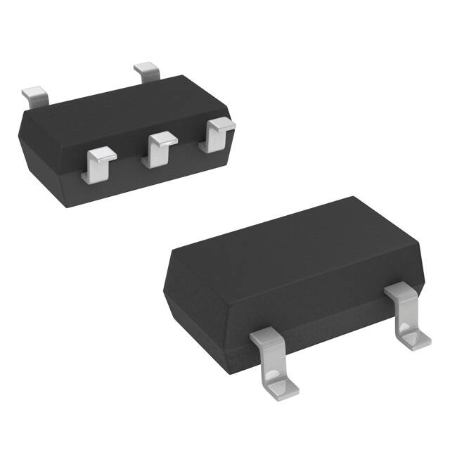
Packages : SOT-25, SOT- 89, SOT-89-5, SOP8FD, USP-6C, SOT-223, and TO-252
EU RoHS Compliant, Pb Free
The IXD1216 is positive voltage regulator with
operation voltage up to 28V, manufactured by CMOS
process.
The IC consists of a voltage reference, an error
amplifier, a current limiter, a thermal protection, a
phase compensation circuit, and a driver transistor.
The output voltage is selectable in 0.1 V increments
within the range from 2.0 V to 12 V for B and D series
and from 2.0 V to 23 V with external resistors for C
series. High precision output voltage achieved by
laser trimming technology.
The IXD1216 is stable with low ESR ceramic output
capacitor (CL). The over current protection circuit and
the thermal shutdown are built-in. These two
protection circuits operate when the output current
reaches current limit level or the junction temperature
reaches temperature limit.
The Chip Enable (CE) function allows set IXD1216
into standby mode, reducing current consumption to
less than 0.1 µA typically.
The IXD1216 is available in SOT-25, SOT-89, SOT89-5, SOP-8FD, USP-6C, SOT-223, and TO-252
packages.
APPLICATIONS
Mobile phones
Car Audio and Navigation Systems
Cameras, VCRs
Various portable equipment
TYPICAL APPLICATION CIRCUIT
TYPICAL PERFORMANCE CHARACTERISTIC
Output Voltage vs. Input Voltage (IXD1216B/D502)
CIN = CL = 1 µF, Ta = 250C,
The IXD1216B with CE function
The IXD1216C series
PS033901-0515
PRELIMINARY
1
�Product Specification
IXD1216
ABSOLUTE MAXIMUM RATINGS
SYMBOL
RATINGS
Input Voltage
PARAMETER
VIN
– 0.3 ~ +30
V
Output Current
IOUT
3001)
mA
Output Voltage
CE Input Voltage (IXD1216B/C version
only)
FB Voltage (IXD1216C version only)
VOUT
– 0.3 ~ VIN + 0.3 or +302)
V
– 0.3 ~ VIN + 0.3 or +30
2)
V
– 0.3 ~ VIN + 0.3 or +30
2)
V
VCE
VFB
250
SOT-25
600 (PCB mounted)
500
SOT-89
1000 (PCB mounted)
500
SOT-89-5
Power Dissipation
2)
USP-6C
1300 (PCB mounted)
PD
mW
1500 (PCB mounted)
500
TO-252
1800 (PCB mounted)
300
SOP-8FD
Storage Temperature Range
120
1000 (PCB mounted)
300
SOT223
Operating Temperature Range
UNITS
1500 (PCB mounted)
TOPR
TSTG
– 40 ~ + 85
0
– 55 ~ +125
0
C
C
All voltages are in respect to VSS
1) IOUT ≤ Pd/ (VIN-VOUT)
2) The lowest value between VIN + 0.3 and 30 V
3) This is a reference data taken by using the test board. Please refer to page 24 to 30 for details
PS033901-0515
PRELIMINARY
2
�Product Specification
IXD1216
ELECTRICAL OPERATING CHARACTERISTICS
Ta = 25 0C
PARAMETER
Input Voltage
SYMBOL
VIN
Output Voltage
VOUT(E)1)
Maximum Output Current
IOUT_MAX
Load Regulation
∆VOUT
VDIF1
Dropout Voltage2)
VDIF2
Supply Current
Standby Current
CONDITIONS
ISS
ISTB
Line Regulation
Output Voltage Temperature
Characteristics
MIN.
TYP.
MAX.
UNIT
CIRCUIT
28.0
V
2.04
2.02
V
mA
mV
mV
µA
µA
%/V
± 100
ppm/0C
2.0
VCE = VIN, IOUT = 20 mA5)
2% accuracy
VFB = VCE = VIN = 4.0 V,
IOUT = 20 mA6)
1 % accuracy
VOUT(T) ≥ 3 V
VCE = VIN = VOUT(T) + 3 V
VOUT(T) < 3 V
2.0 V ≤ VOUT(T) ≤ 7.0 V
VCE = VIN, 1 mA ≤
IOUT ≤ 50 mA
7.1 V ≤ VOUT(T) ≤ 12.0 V
VCE = VIN, IOUT = 20 mA
VCE = VIN, VFB = VOUT, IOUT = 20 mA6)
VCE = VIN, IOUT = 100 mA
VCE = VIN, VFB = VOUT, IOUT = 100 mA6)
VCE = VIN
VCE = 0 V
IOUT = 5 mA
VOUT(T) + 2 V ≤ VIN ≤ 28 V,
VCE = VIN
IOUT = 13 mA
VCE = VIN, IOUT = 30 mA
- 40 0C ≤ TOPR ≤ 85 0C
1.96
1.98
150
100
1
E-0
2.00
2.00
50
110
E-14)
450
E-24)
1900
5
0.01
0.05
0.15
90
140
600
2600
9
0.10
0.10
0.30
Power Supply Rejection Ratio
PSRR
VCE = VIN, IOUT = 20 mA, f = 1 kHz
VIN = (VOUT)T) + 2) VDC + 0.5 V p-pAC
30
dB
Short Circuit Current
Thermal Shutdown Detect
Temperature
Thermal Shutdown
Hystetresis
CE “H” Level Voltage5)
CE “L” Level Voltage5)
CE “H” Level Current5)
CE “L” Level Current5)
FB Pin Resistance
ISHORT
VCE = VIN , VIN = VOUT)T) + 2 V
30
mA
TTSD
Junction Temperature
THYS
VCEH
VCEL
ICEH
ICEL
RFB
VCE = VIN = 28.0 V
VIN = 28.0 V, VCE = VSS
VFB = VIN = VOUT = 5.0 V, VCE = VSS
1.1
0
-0.1
-0.1
1.70
150
0
25
0
4.10
C
C
VIN
0.35
0.1
0.1
6.30
V
V
µA
µA
MΩ
NOTE:
Unless otherwise stated, VIN = VCE = VOUT (T) +2.0 V
1) VOUT (T) is Nominal output voltage and VOUT (E) is Effective output voltage, (I.e. the output voltage when "VOUT (T) +1.0V" is provided at the
VIN pin, while maintaining a certain IOUT value).
2) VDIF = {VIN-VOUT}, where VIN1 is the input voltage when VOUT = 0.98 VOUT(T) appears, while input voltage gradually decreases
3) Refer to the Table “Voltage Chart, Output Voltage”
4) Refer to the Table “Voltage Chart, Dropout Voltage”
5) IXD1216B/C versions only
6) IXD1216C version only
PS033901-0515
PRELIMINARY
3
�Product Specification
IXD1216
ELECTRICAL OPERATING CHARACTERISTICS (CONTINUED)
Voltage Chart
Ta = 250C
SYMBOL
E-0
OUTPUT
VOLTAGE
VOUT(T)
(V)
2.0
2.1
2.2
2.3
2.4
2.5
2.6
2.7
2.8
2.9
3.0
3.1
3.2
3.3
3.4
3.5
3.6
3.7
3.8
3.9
4.0
4.1
4.2
4.3
4.4
4.5
4.6
4.7
4.8
4.9
5.0
5.1
5.2
5.3
5.4
5.5
5.6
5.7
5.8
5.9
6.0
6.1
6.2
6.3
6.4
6.5
6.6
6.7
6.8
6.9
7.0
OUTPUT VOLTAGE, V
VOUT (E)
2% accuracy
1% accuracy
MIN.
MAX.
MIN.
MAX.
1.960
2.040
1.980
2.020
2.058
2.142
2.079
2.121
2.156
2.244
2.178
2.222
2.254
2.346
2.277
2.323
2.352
2.448
2.376
2.424
2.450
2.550
2.475
2.525
2.548
2.652
2.574
2.626
2.646
2.754
2.673
2.727
2.744
2.856
2.772
2.828
2.842
2.958
2.871
2.929
2.940
3.060
2.970
3.030
3.038
3.162
3.069
3.131
3.136
3.264
3.168
3.232
3.234
3.366
3.267
3.333
3.332
3.468
3.366
3.434
3.430
3.570
3.465
3.535
3.528
3.672
3.564
3.636
3.626
3.774
3.663
3.737
3.724
3.876
3.762
3.838
3.822
3.978
3.861
3.939
3.920
4.080
3.960
4.040
4.018
4.182
4.059
4.141
4.116
4.284
4.158
4.242
4.214
4.386
4.257
4.343
4.312
4.488
4.356
4.444
4.410
4.590
4.455
4.545
4.508
4.692
4.554
4.646
4.606
4.794
4.653
4.747
4.704
4.896
4.752
4.848
4.802
4.998
4.851
4.949
4.900
5.100
4.950
5.050
4.998
5.202
5.049
5.151
5.096
5.304
5.148
5.252
5.194
5.406
5.247
5.353
5.292
5.508
5.346
5.454
5.390
5.610
5.445
5.555
5.488
5.712
5.544
5.656
5.586
5.814
5.643
5.757
5.684
5.916
5.742
5.916
5.782
6.018
5.841
5.959
5.880
6.120
5.940
6.060
5.978
6.222
6.039
6.161
6.076
6.324
6.138
6.262
6.174
6.426
6.237
6.363
6.272
6.528
6.336
6.464
6.370
6.630
6.435
6.565
6.468
6.732
6.534
6.666
6.566
6.834
6.633
6.767
6.664
6.936
6.732
6.868
6.762
7.038
6.831
6.969
6.860
7.140
6.930
7.070
PS033901-0515
E-1
DROPOUT VOLTAGE, mV
IOUT = 20 mA
Vdif1
TYP.
MAX.
450
600
450
600
390
520
390
520
390
520
310
450
310
450
310
450
310
450
310
450
260
360
260
360
260
360
260
360
260
360
260
360
260
360
260
360
260
360
260
360
220
320
220
320
220
320
220
320
220
320
220
320
220
320
220
320
220
320
220
320
190
280
190
280
190
280
190
280
190
280
190
280
190
280
190
280
190
280
190
280
190
280
190
280
190
280
190
280
190
280
170
230
170
230
170
230
170
230
170
230
170
230
PRELIMINARY
E-2
DROPOUT VOLTAGE, mV
IOUT = 100 mA
Vdif2
TYP.
MAX.
1900
2600
1900
2600
1700
2200
1700
2200
1700
2200
1500
1900
1500
1900
1500
1900
1500
1900
1500
1900
1300
1700
1300
1700
1300
1700
1300
1700
1300
1700
1300
1700
1300
1700
1300
1700
1300
1700
1300
1700
1100
1500
1100
1500
1100
1500
1100
1500
1100
1500
1100
1500
1100
1500
1100
1500
1100
1500
1100
1500
1000
1300
1000
1300
1000
1300
1000
1300
1000
1300
1000
1300
1000
1300
1000
1300
1000
1300
1000
1300
1000
1300
1000
1300
1000
1300
1000
1300
1000
1300
800
1150
800
1150
800
1150
800
1150
800
1150
800
1150
4
�Product Specification
IXD1216
ELECTRICAL OPERATING CHARACTERISTICS (CONTINUED)
Voltage Chart (Continued)
SYMBOL
E-0
E-1
E-2
OUTPUT
VOLTAGE
VOUT(T)
(V)
7.1
7.2
7.3
7.4
7.5
7.6
7.7
7.8
7.9
8.0
8.1
8.2
8.3
8.4
8.5
8.6
8.7
8.8
8.9
9.0
9.1
9.2
9.3
9.4
9.5
9.6
9.7
9.8
9.9
10.0
10.1
10.2
10.3
10.4
10.5
10.6
10.7
10.8
10.9
11.0
11.1
11.2
11.3
11.4
11.5
11.6
11.7
11.8
11.9
12.0
OUTPUT VOLTAGE, V
VOUT (E)
2% accuracy
1% accuracy
MIN.
MAX.
MIN.
MAX.
6.958
7.242
7.029
7.171
7.056
7.344
7.128
7.272
7.154
7.446
7.227
7.373
7.252
7.548
7.326
7.474
7.350
7.650
7.425
7.575
7.448
7.752
7.524
7.676
7.546
7.854
7.623
7.777
7.644
7.956
7.722
7.878
7.742
8.058
7.821
7.979
7.840
8.160
7.920
8.080
7.938
8.262
8.019
8.181
8.036
8.364
8.118
8.282
8.134
8.466
8.217
8.383
8.232
8.568
8.316
8.484
8.330
8.670
8.415
8.585
8.428
8.772
8.514
8.686
8.526
8.874
8.613
8.787
8.624
8.976
8.712
8.888
8.722
9.078
8.811
8.989
8.820
9.180
8.910
9.090
8.918
9.282
9.009
9.191
9.016
9.384
9.108
9.292
9.114
9.486
9.207
9.393
9.212
9.588
9.306
9.494
9.310
9.690
9.405
9.595
9.408
9.792
9.504
9.696
9.506
9.894
9.603
9.797
9.604
9.996
9.702
9.898
9.702
10.098
9.801
9.999
9.800
10.200
9.900
10.100
9.898
10.302
9.999
10.201
9.996
10.404
10.098
10.302
10.094
10.506
10.197
10.403
10.192
10.608
10.296
10.504
10.290
10.710
10.395
10.605
10.388
10.812
10.494
10.706
10.486
10.914
10.593
10.807
10.584
11.016
10.692
10.908
10.682
11.118
10.791
11.009
10.780
11.220
10.890
11.110
10.878
11.322
10.989
11.211
10.976
11.424
11.088
11.312
11.074
11.526
11.187
11.413
11.172
11.628
11.286
11.514
11.270
11.730
11.385
11.615
11.368
11.832
11.484
11.716
11.466
11.934
11.583
11.817
11.564
12.036
11.682
11.918
11.662
12.138
11.781
12.019
11.760
12.240
11.880
12.120
DROPOUT VOLTAGE, mV
IOUT = 20 mA
Vdif1
TYP.
MAX.
170
230
170
230
170
230
170
230
170
230
170
230
170
230
170
230
170
230
170
230
130
190
130
190
130
190
130
190
130
190
130
190
130
190
130
190
130
190
130
190
130
190
130
190
130
190
130
190
130
190
130
190
130
190
130
190
130
190
130
190
120
160
120
160
120
160
120
160
120
160
120
160
120
160
120
160
120
160
120
160
120
160
120
160
120
160
120
160
120
160
120
160
120
160
120
160
120
160
120
160
DROPOUT VOLTAGE, mV
IOUT = 100 mA
Vdif2
TYP.
MAX.
800
1150
800
1150
800
1150
800
1150
800
1150
800
1150
800
1150
800
1150
800
1150
800
1150
700
950
700
950
700
950
700
950
700
950
700
950
700
950
700
950
700
950
700
950
700
950
700
950
700
950
700
950
700
950
700
950
700
950
700
950
700
950
700
950
650
850
650
850
650
850
650
850
650
850
650
850
650
850
650
850
650
850
650
850
650
850
650
850
650
850
650
850
650
850
650
850
650
850
650
850
650
850
650
850
PS033901-0515
PRELIMINARY
5
�Product Specification
IXD1216
PIN CONFIGURATION
The dissipation pad for the
USP-6C package should be
solder-plated in respect with
mounting pattern and metal
mask to improve heat
dissipation and. mounting
strength. If the pad needs to
be connected to other pins,
it should be connected to
the VSS (No. 5) pin.
SOT-25 (TOP VIEW)
SOT-89 (TOP VIEW)
SOT-223 (TOP VIEW)
SOT-89-5 (TOP VIEW)
TO-252 (TOP VIEW)
USP-6C (BOTTOM VIEW)
SOP-8FD (TOP VIEW)
PIN ASSIGNMENT
SOT-25
1
2
5
SOT-89
3
2
1
PIN NUMBER
SOT-89-5 USP-6C SOT-223
3
5
6
2
2
5
1
1
1
4
3
3
3
4
2
4
1)
TO-252
1
2
3
SOP-8FD
8
6
1
4
2, 3, 7
5
PIN NAME
VIN
VSS
VOUT
CE
NC
FUNCTIONS
Power Input
Ground
Output Voltage
ON/OFF Control LOW – Standby mode,
HIGH – Active1)
No Connection
No Connection (B series)/FB (C series)
CE pin does not have internal pull-down resistor. IC state is undefined, if this pin is open.
BLOCK DIAGRAMS
IXD1216B
IXD1216C
IXD1216D
Diodes inside the circuits are ESD protection diodes and parasitic diodes.
PS033901-0515
PRELIMINARY
6
�Product Specification
IXD1216
BASIC OPERATION
The Error Amplifier of the IXD1216 series monitors output voltage divided by internal resistors R1 & R2 and
compares it with the internal Reference Voltage (see Block Diagram above). The output signal from error amplifier
drives gate of the P-channel MOSFET, which is connected to the V OUT pin and operates as a series voltage
regulator.
The Current Limit/Short Protection circuits monitor level of the output current, and Thermal shutdown circuit
monitors MOSFET junction temperature to prevent IC damage by excessive current.
The CE pin allows shutdown internal circuitry to minimize power consumption.
Current Limiter, Short-Circuit Protection
The IXD1216 series have a current limiter circuit & a fold back circuit, which aid the operations of the current limiter
and circuit protection. When the load current reaches the current limit level, the fixed current limiter circuit activates
and output voltage drops. Because of this drop, the fold back circuit activates too, and output voltage drops further
decreasing output current. When the output pin is shorted, a current of about 30 mA flows.
Thermal Shutdown
When the junction temperature of the built-in transistor reaches the temperature limit, the thermal shutdown circuit
activates and turns transistor OFF. The IC resumes normal operation when the junction temperature falls below
value determined by Thermal Shutdown Hysteresis.
CE Pin
The CE pin allows shutdown internal circuitry to minimize power consumption. In shutdown mode, output at the
VOUT pin is pulled down to the VSS level by resistors R1 and R2 connected in series.
Note that the CE input is active HIGH and has no pull down resistor. IC will be in undefined state, if CE pin is open.
CE pin should be connected to either VIN or ground. IC current consumption may increase, if voltage applied to this
pin is ~ 0.5 of VIN.
Minimum Operating Voltage
The input voltage should be above 2.0 V for the stable IC operation.
TYPICAL APPLICATION CIRCUIT
IXD1216B version
IXD1216C version
IXD1216D version
LAYOUT AND USE CONSIDERATIONS
1. Mount external component as close to the IC as possible and use thick, short connecting traces to
reduce the circuit impedance.
2. The IC may malfunction if absolute maximum ratings are exceeded.
3. If power source of this regulator is a high impedance device, an input capacitor CIN ≥ 0.1μF should be
used to prevent oscillations.
4. The internal phase compensation guarantees the IXD1216 stable operations even without load
capacitor CL. However, load capacitor CL = 0.1 – 1.0 µF located as close to VOUT and VSS pins may
improve regulator’s dynamic characteristics, reducing over/undershoot at heavy load.
5. In case of high output current, increasing the input capacitor value can stabilize operations.
6. Please ensure that output current IOUT is less than PD / (VIN - VOUT), where PD is a rated power
dissipation value of the package shown at ABSOLUTE MAXIMUM RATING table to not exceed it.
7. The IXD1216C version requires external resistive divider to set output voltage above 2.0 V. Output
voltage determined by resistors R21/R22 as well as resistance of the internal resistive divider RFB, which
is in the range from 1.7 MΩ to 6.3 MΩ.
PS033901-0515
PRELIMINARY
7
�Product Specification
IXD1216
Component R21/RFB determines error in voltage setting and it should be taken into considerations, if R21
value is close to value of RFB. If R21 is less than 10 kΩ, this error is negligible.
Example:
If R21 = 64.9 kΩ and R22 = 100 kΩ, output voltage may vary from part to part due difference in RFB from
3.318 V to 3.374 V.
If R21 = 6.49 Ω and R22 = 10 kΩ, output voltage will vary from part to part due difference in RFB from
3.300 V to 3.306 V.
TEST CIRCUITS
Circuit
IXD1216B
IXD1216C
IXD1216D
IXD1216C
IXD1216D
Circuit
IXD1216B
Circuit
IXD1216B
IXD2116C
IXD1216D
Circuit
IXD1216C
Unless otherwise stated, Ta = 250C, VCE = VIN, CIN = CL = 1 µF (ceramic)
The IXD1216D has CE pin connected to VIN internally.
PS033901-0515
PRELIMINARY
8
�Product Specification
IXD1216
TYPICAL PERFORMANCE CHARACTERISTICS
(1) Output Voltage vs. Output Current
IXD1216x202xx
IXD1216x202xx
VIN = VCE = 5.0 V
VIN = VCE, Ta = 250C
IXD1216B/D 332xx
IXD1216B/D 332xx
VIN = VCE = 6.3 V
VIN = VCE, Ta = 250C
IXD1216B/D 502xx
IXD1216B/D 502xx
VIN = VCE = 8.0 V
VIN = VCE, Ta = 250C
TYPICAL PERFORMANCE CHARACTERISTICS (Continued)
PS033901-0515
PRELIMINARY
9
�Product Specification
IXD1216
(1) Output Voltage vs Output Current (Continue)
Topr = 25 0C
IXD1216B/D C02xx
IXD1216B/D C02xx
VIN = VCE = 15.0 V
VIN = VCE, Ta = 250C
(2) Output Voltage vs. Input Voltage
IXD1216x202xx
IXD1216x202xx
IXD1216B/D 332xx
IXD1216B/D 332xx
VIN = VCE, Ta = 250C
VIN = VCE, Ta = 250C
PS033901-0515
VIN = VCE, Ta = 250C
VIN = VCE, Ta = 250C
PRELIMINARY
10
�Product Specification
IXD1216
TYPICAL PERFORMANCE CHARACTERISTICS (Continued)
(2) Output Voltage vs. Input Voltage
IXD1216B/D 502xx
IXD1216B/D 502xx
VIN = VCE , Ta = 250C
VIN = VCE , Ta = 250C
IXD1216B/D C02xx
IXD1216B/D C02xx
VIN = VCE , Ta = 250C
VIN = VCE , Ta = 250C
(3) Dropout Voltage vs. Output Current
IXD1216x202xx
PS033901-0515
IXD1216B/D 332xx
PRELIMINARY
11
�Product Specification
IXD1216
TYPICAL PERFORMANCE CHARACTERISTICS (Continued)
(3) Dropout Voltage vs. Output Current (Continued)
IXD1216B/D 502xx
IXD1216B/D C02xx
(4) Supply Current vs. Input Voltage
IXD1216x202xx
IXD1216x202xx
VIN = VCE
VIN = VCE = 4.0 V
IXD1216B/D 332xx
IXD1216B/D 332xx
VIN = VCE
VIN = VCE = 5.3 V
PS033901-0515
PRELIMINARY
12
�Product Specification
IXD1216
TYPICAL PERFORMANCE CHARACTERISTICS (Continued)
(4) Supply Current vs. Input Voltage (Continued)
IXD1216B/D 502xx
IXD1216B/D 502xx
VIN = VCE
VIN = VCE = 7.0 V
IXD1216B/D C02xx
IXD1216B/D C02xx
VIN = VCE
VIN = VCE = 14.0 V
(5) Output Voltage vs. Ambient Temperature
IXD1216x202xx
IXD1216B/D 332xx
VIN = VCE = 4.0 V
VIN = VCE = 5.3 V
PS033901-0515
PRELIMINARY
13
�Product Specification
IXD1216
TYPICAL PERFORMANCE CHARACTERISTICS (Continued)
(5) Output Voltage vs. Ambient temperature (Continued)
IXD1216B/D 502xx
IXD1216B/D C02xx
VIN = VCE = 7.0 V
VIN = VCE = 14.0 V
(6) Input Voltage Transient Response
IXD1216x202xx
IXD1216x202xx
IOUT = 1 mA, Ta = 250C, tR = tF = 5 µs, VIN = 4.0 V 5.0 V
IOUT = 30 mA, Ta = 250C, tR = tF = 5 µs, VIN = 4.0 V 5.0 V
IXD1216B/D 332xx
IXD1216B/D 332xx
IOUT = 1 mA, Ta = 250C, tR = tF = 5 µs, VIN = 5.3 V 6.3 V
IOUT = 30 mA, Ta = 250C, tR = tF = 5 µs, VIN = 5.3 V 6.3 V
PS033901-0515
PRELIMINARY
14
�Product Specification
IXD1216
TYPICAL PERFORMANCE CHARACTERISTICS (Continued)
(6) Input Voltage Transient Response (Continued)
IXD1216B/D 502xx
IXD1216B/D 502xx
IOUT = 1 mA, Ta = 250C, tR = tF = 5 µs, VIN = 7.0 V 8.0 V
IOUT = 30 mA, Ta = 250C, tR = tF = 5 µs, VIN = 7.0 V 8.0 V
IXD1216B/D C02xx
IXD1216B/D C02xx
IOUT = 1 mA, Ta = 250C, tR = tF = 5 µs, VIN = 14.0 V 15.0 V
IOUT = 30 mA, Ta = 250C, tR = tF = 5 µs, VIN = 14.0 V 15.0 V
(7) Load Transient Response
IXD1216x202xx
IXD1216B/D 332xx
Ta = 250C, tR = tF = 5 µs, VIN = 4.0 V IOUT = 1 mA, 30 mA
Ta = 250C, tR = tF = 5 µs, VIN = 4.0 V IOUT = 1 mA, 30 mA
PS033901-0515
PRELIMINARY
15
�Product Specification
IXD1216
TYPICAL PERFORMANCE CHARACTERISTICS (Continued)
(7) Load Transient Response (Continued)
IXD1216B/D 502xx
IXD1216B/D C02xx
Ta = 250C, tR = tF = 5 µs, VIN = 7.0 V IOUT = 1 mA, 30 mA
Ta = 250C, tR = tF = 5 µs, VIN = 14.0 V IOUT = 1 mA, 30 mA
(8) Input Voltage Rising Response Time
IXD1216x202xx
IXD1216x202xx
Ta = 250C, tR = 5 µs, VIN = 0 4.0 V IOUT = 1 mA,
Ta = 250C, tR = 5 µs, VIN = 0 4.0 V IOUT = 30 mA,
IXD1216B/D 332xx
IXD1216B/D 332xx
Ta = 250C, tR = 5 µs, VIN = 0 5.3 V IOUT = 1 mA,
Ta = 250C, tR = 5 µs, VIN = 0 5.3 V IOUT = 30 mA,
PS033901-0515
PRELIMINARY
16
�Product Specification
IXD1216
TYPICAL PERFORMANCE CHARACTERISTICS (Continued)
(8) Input Voltage Rising Response Time (Continued)
IXD1216B/D 502xx
IXD1216B/D 502xx
Ta = 250C, tR = 5 µs, VIN = 0 7.0 V IOUT = 1 mA,
Ta = 250C, tR = 5 µs, VIN = 0 7.0 V IOUT = 30 mA
IXD1216B/D C02xx
IXD1216B/D C02xx
Ta = 250C, tR = 5 µs, VIN = 0 14.0 V IOUT = 1 mA,
Ta = 250C, tR = 5 µs, VIN = 0 14.0 V IOUT = 30 mA
(9) CE Rising Response Time
IXD1216x202xx
IXD1216x202xx
Ta = 250C, tR = 5 µs, VIN = 4.0 V, VCE = 0 4.0 V IOUT = 1 mA
Ta = 250C, tR = 5 µs, VIN = 4.0 V, VCE = 0 4.0 V IOUT = 30 mA
PS033901-0515
PRELIMINARY
17
�Product Specification
IXD1216
TYPICAL PERFORMANCE CHARACTERISTICS (Continued)
(9) CE Rising Response Time (Continued)
IXD1216B/D 332xx
IXD1216B/D 332xx
Ta = 250C, tR = 5 µs, VIN = 5.3 V, VCE = 0 VIN, IOUT = 1 mA,
Ta = 250C, tR = 5 µs, VIN = 5.3 V, VCE = 0 VIN, IOUT = 30 mA
IXD1216B/D 502xx
IXD1216B/D 502xx
Ta = 250C, tR = 5 µs, VIN = 7.0 V, VCE = 0 VIN, IOUT = 1 mA,
Ta = 250C, tR = 5 µs, VIN = 7.0 V, VCE = 0 VIN, IOUT = 30 mA
IXD1216B/D C02xx
IXD1216B/D C02xx
Ta = 250C, tR = 5 µs, VIN = 14.0 V, VCE = 0 VIN, IOUT = 1 mA,
Ta = 250C, tR = 5 µs, VIN = 14.0 V, VCE = 0 VIN, IOUT = 30 mA
PS033901-0515
PRELIMINARY
18
�Product Specification
IXD1216
TYPICAL PERFORMANCE CHARACTERISTICS (Continued)
(10) Power Supply Ripple Rejection
IXD1216x202xx
IXD1216x202xx
Ta = 250C, VIN = VCE = 4.0 V+ 0.5 Vp-pAC, IOUT = 1 mA,
Ta = 250C, VIN = VCE = 4.0 V+ 0.5 Vp-pAC, IOUT = 30 mA,
IXD1216B/D 332xx
IXD1216B/D 332xx
Ta = 250C, VIN = VCE = 5.3 V+ 0.5 Vp-pAC, IOUT = 1 mA,
Ta = 250C, VIN = VCE = 5.3 V+ 0.5 Vp-pAC, IOUT = 1 mA,
IXD1216B/D 502xx
IXD1216B/D 502xx
Ta = 250C, VIN = VCE = 7.0 V+ 0.5 Vp-pAC, IOUT = 1 mA,
Ta = 250C, VIN = VCE = 7.0 V+ 0.5 Vp-pAC, IOUT = 1 mA,
PS033901-0515
PRELIMINARY
19
�Product Specification
IXD1216
TYPICAL PERFORMANCE CHARACTERISTICS (Continued)
(10) Power Supply Ripple Rejection (Continued)
IXD1216B/D C02xx
IXD1216B/D C02xx
Ta = 250C, VIN = VCE = 7.0 V+ 0.5 Vp-pAC, IOUT = 1 mA,
Ta = 250C, VIN = VCE = 7.0 V+ 0.5 Vp-pAC, IOUT = 30 mA,
ORDERING INFORMATION
IXD1216-
DESIGNATOR
DESCRIPTION
Type and Options
SYMBOL
DESCRIPTION
B
Fixed Output Voltage 2.0 – 12.0 V in 0.1 V increments, CE Function
C
Output Voltage Set Externally (VFB = 2.0 V), CE Function
D
Output Voltage
20 – C0
Output Voltage
Accuracy
2
Fixed Output Voltage 2.0 – 12.0 V in 0.1 V increments, No CE function (3-pin regulator)
For voltages from 2.0 V to 9.9 V, e.g. 2.5 V - = 2, = 5; 5.0 V - = 5, = 0
For voltages from 10.0 V to 12.0 V, e.g. 10.6 V - = A = 6; 12.0 V - = C, = 0
Accuracy: ±2%
1
Accuracy: ±1%
-
(*)
Packages1)
(Order Limit)
MR
SOT-25 (3000/Reel)
MR-G
SOT-25 (3000/Reel)
PR
SOT-89, SOT-89-5 (1000/Reel)
PR-G
SOT-89, SOT-89-5 (1000/Reel)
ER
USP-6C (3000/Reel)
ER-G
USP-6C (3000/Reel)
FR
SOT-223 (1000/Reel)
FR-G
SOT-223 (1000/Reel)
JR
TO-252 (2500/reel)
JR-G
TO-252 (2500/reel)
QR-G
SOP-8FD (1000/reel)
NOTE:
The “-G” suffix denotes Halogen and Antimony free as well as being fully RoHS compliant.
1) IXD1216B/C versions are available in SOT-25, SOT-89-5, USP-6C, and SOP-8FD packages only; IXD1216D version is
available in SOT-89, SOT-223, and TO-252 packages only.
PS033901-0515
PRELIMINARY
20
�Product Specification
IXD1216
PACKAGE DRAWING AND DIMENSIONS
Units: mm
SOT-25
SOT-89
SOT-89-5
SOT-223
PS033901-0515
PRELIMINARY
21
�Product Specification
IXD1216
PACKAGE DRAWING AND DIMENSIONS (CONTINUED)
Units: mm
TO-252
USP-6C
USP-6C Reference Pattern Layout
USP-6C Reference Metal Mask Design
PS033901-0515
PRELIMINARY
22
�Product Specification
IXD1216
PACKAGE DRAWING AND DIMENSIONS (CONTINUED)
Units: mm
SOP-8FD
PS033901-0515
SOP-8FD Reference Pattern Layout
PRELIMINARY
23
�Product Specification
IXD1216
PACKAGE POWER DISSIPATION
SOT-25 Power Dissipation
The power dissipation varies with the mount board conditions.
Please use this data as a reference only.
1. Measurement Conditions:
Condition:
Ambient:
Soldering:
Board:
Material:
Thickness:
Through-hole:
Mount on a board
Natural convection
Lead (Pb) free
Dimensions 40×40 mm (1600 mm2 in one side)
Copper (Cu) traces occupy 50% of the board area
on top and bottom layers
Package heat sink tied to the copper traces.
(Board of SOT-26 is used)
Glass Epoxy (FR-4)
1.6 mm
4 x 0.8 Diameter
2. Power Dissipation vs. Ambient Temperature
Board Mount (Tjmax = 125 0C)
Ambient
Temperature, 0C
Power Dissipation
Pd, mW
Thermal Resistance,
0
C/W
25
85
600
240
166.67
PS033901-0515
PRELIMINARY
24
�Product Specification
IXD1216
PACKAGE POWER DISSIPATION (CONTINUED)
SOT-89 Power Dissipation
The power dissipation varies with the mount board conditions.
Please use this data as a reference only.
1. Measurement Conditions:
Condition:
Ambient:
Soldering:
Board:
Material:
Thickness:
Through-hole:
Mount on a board
Natural convection
Lead (Pb) free
Dimensions 40×40 mm (1600 mm2 in one side)
Copper (Cu) traces occupy 50% of the board area
on top and bottom layers
Package heat sink tied to the copper traces.
Glass Epoxy (FR-4)
1.6 mm
5 x 0.8 Diameter
2. Power Dissipation vs. Ambient Temperature
Board Mount (Tjmax = 125 0C)
Ambient
Temperature, 0C
Power Dissipation
Pd, mW
Thermal Resistance,
0
C/W
25
85
1000
400
100.00
PS033901-0515
PRELIMINARY
25
�Product Specification
IXD1216
PACKAGE POWER DISSIPATION (CONTINUED)
SOT-89-5 Power Dissipation
The power dissipation varies with the mount board conditions.
Please use this data as a reference only.
1. Measurement Conditions:
Condition:
Ambient:
Soldering:
Board:
Material:
Thickness:
Through-hole:
Mount on a board
Natural convection
Lead (Pb) free
Dimensions 40×40 mm (1600 mm2 in one side)
Copper (Cu) traces occupy 50% of the board area
on top and bottom layers
Package heat sink tied to the copper traces.
Glass Epoxy (FR-4)
1.6 mm
5 x 0.8 Diameter
2. Power Dissipation vs. Ambient Temperature
Board Mount (Tjmax = 125 0C)
Ambient
Temperature, 0C
Power Dissipation
Pd, mW
Thermal Resistance,
0
C/W
25
85
1300
500
76.92
PS033901-0515
PRELIMINARY
26
�Product Specification
IXD1216
PACKAGE POWER DISSIPATION (CONTINUED)
USP-6C Power Dissipation
The power dissipation varies with the mount board conditions.
Please use this data as a reference only.
1. Measurement Conditions:
Condition:
Ambient:
Soldering:
Board:
Mount on a board
Natural convection
Lead (Pb) free
Dimensions 40×40 mm (1600 mm2 in one side)
Copper (Cu) traces occupy 50% of the board
area
Material:
Thickness:
Through-hole:
on top and bottom layers
Package heat sink teed to copper traces
Glass Epoxy (FR-4)
1.6 mm
4 x 0.8 Diameter
2. Power Dissipation vs. Ambient Temperature
Board Mount (Tjmax = 125 0C)
Ambient
Temperature, 0C
Power Dissipation
Pd, mW
Thermal Resistance,
0
C/W
25
85
1000
400
100.00
PS033901-0515
PRELIMINARY
27
�Product Specification
IXD1216
PACKAGE POWER DISSIPATION (CONTINUED)
SOT-223 Power Dissipation
The power dissipation varies with the mount board conditions.
Please use this data as a reference only.
1. Measurement Conditions:
Condition:
Ambient:
Soldering:
Board:
Material:
Thickness:
Through-hole:
Mount on a board
Natural convection
Lead (Pb) free
Dimensions 40×40 mm (1600 mm2 in one side)
Copper (Cu) traces occupy 50% of the board area
on top and bottom layers
Package heat sink tied to the copper traces.
Glass Epoxy (FR-4)
1.6 mm
4 x 0.8 Diameter
2. Power Dissipation vs. Ambient Temperature
Board Mount (Tjmax = 125 0C)
Ambient
Temperature, 0C
Power Dissipation
Pd, mW
Thermal Resistance,
0
C/W
25
85
1500
600
66.67
PS033901-0515
PRELIMINARY
28
�Product Specification
IXD1216
PACKAGE POWER DISSIPATION (CONTINUED)
TO-252 Power Dissipation
The power dissipation varies with the mount board conditions.
Please use this data as a reference only.
1. Measurement Conditions:
Condition:
Ambient:
Soldering:
Board:
Material:
Thickness:
Through-hole:
Mount on a board
Natural convection
Lead (Pb) free
Dimensions 40×40 mm (1600 mm2 in one side)
Copper (Cu) traces occupy 50% of the board area
on top and bottom layers
Package heat sink tied to the copper traces.
Glass Epoxy (FR-4)
1.6 mm
4 x 0.8 Diameter
2. Power Dissipation vs. Ambient Temperature
Board Mount (Tjmax = 125 0C)
Ambient
Temperature, 0C
Power Dissipation
Pd, mW
Thermal Resistance,
0
C/W
25
85
1800
720
55.56
PS033901-0515
PRELIMINARY
29
�Product Specification
IXD1216
PACKAGE POWER DISSIPATION (CONTINUED)
SOP-8FD Power Dissipation
The power dissipation varies with the mount board conditions.
Please use this data as a reference only.
1. Measurement Conditions:
Condition:
Ambient:
Soldering:
Board:
Material:
Thickness:
Through-hole:
Mount on a board
Natural convection
Lead (Pb) free
Dimensions 40×40 mm (1600 mm2 in one side)
Copper (Cu) traces occupy 50% of the board area
on top and bottom layers
Package heat sink tied to the copper traces.
Glass Epoxy (FR-4)
1.6 mm
4 x 0.8 Diameter
2. Power Dissipation vs. Ambient Temperature
Board Mount (Tjmax = 125 0C)
Ambient
Temperature, 0C
Power Dissipation
Pd, mW
Thermal Resistance,
0
C/W
25
85
1500
600
66.67
PS033901-0515
PRELIMINARY
30
�Product Specification
IXD1216
MARKING
SOT-25 , SOT-89, SOT89-5, USP-4
SOT-25
SOT-89-5
SOT-223
SOT-89
TO-252
USP-6C
SOP-8FD
- represents product series
MARK
PRODUCT SERIES
2
IXD1216xxxxxx
- represents type of regulator and output voltage range
MARK
TYPE
2
B
3.1 – 6.0
6.1 – 9.0
3
9.1 - 12.0
4
2.0 – 3.0
5
6
D
7
8
PRODUCT SERIES
2.0 – 3.0
0
1
OUTPUT VOLTAGE, V
3.1 – 6.0
IXD1216Bxxxx
IXD1216Dxxxx
6.1 – 9.0
9.1 - 12.0
C
PS033901-0515
2.0
IXD1216Cxxxx
PRELIMINARY
31
�Product Specification
IXD1216
MARKING (CONTINUED)
- represents output voltage
MARK
0
1
2
3
4
5
6
7
8
9
A
B
C
D
E
OUTPUT VOLTAGE, V
-
3.1
3.2
3.3
3.4
3.5
3.6
3.7
3.8
3.9
4.0
4.1
4.2
4.3
4.4
4.5
6.1
6.2
6.3
6.4
6.5
6.6
6.7
6.8
6.9
7.0
7.1
7.2
7.3
7.4
7.5
9.1
9.2
9.3
9.4
9.5
9.6
9.7
9.8
9.9
10.0
10.1
10.2
10.3
10.4
10.5
MARK
12.1
12.2
12.3
12.4
12.5
12.6
12.7
12.8
12.9
13.0
13.1
13.2
13.3
13.4
13.5
15.1
15.2
15.3
15.4
15.5
15.6
15.7
15.8
15.9
16.0
16.1
16.2
16.3
16.4
16.5
F
H
K
L
M
N
P
R
S
T
U
V
X
Y
Z
OUTPUT VOLTAGE, V
-
2.0
2.1
2.2
2.3
2.4
2.5
2.6
2.7
2.8
2.9
3.0
4.6
4.7
4.8
4.9
5.0
5.1
5.2
5.3
5.4
5.5
5.6
5.7
5.8
5.9
6.0
7.6
7.7
7.8
7.9
8.0
8.1
8.2
8.3
8.4
8.5
8.6
8.7
8.8
8.9
9.0
10.6
10.7
10.8
10.9
11.0
11.1
11.2
11.3
11.4
11.5
11.6
11.7
11.8
11.9
12.0
- represents production lot number
01~09, 0A~0Z, 11~9Z, A1~A9, AA~AZ, B1~ZZ in order, (G, I, J, O, Q, W excluded)
PS033901-0515
PRELIMINARY
32
�Product Specification
IXD1216
Customer Support
To share comments, get your technical questions answered, or report issues you may be experiencing with our
products, please visit Zilog’s Technical Support page at http://support.zilog.com. To learn more about this product,
find additional documentation, or to discover other fac-ets about Zilog product offerings, please visit the Zilog
Knowledge Base at http:// zilog.com/kb or consider participating in the Zilog Forum at http://zilog.com/forum. This
publication is subject to replacement by a later edition. To determine whether a later edition exists, please visit the
Zilog website at http://www.zilog.com.
Warning: DO NOT USE THIS PRODUCT IN LIFE SUPPORT SYSTEMS.
LIFE SUPPORT POLICY ZILOG’S PRODUCTS ARE NOT AUTHORIZED FOR USE AS CRITICAL
COMPONENTS IN LIFE SUPPORT DEVICES OR SYSTEMS WITHOUT THE EXPRESS PRIOR WRITTEN
APPROVAL OF THE PRESIDENT AND GENERAL COUNSEL OF ZILOG CORPORATION.
As used herein Life support devices or systems are devices which (a) are intended for surgical implant into the
body, or (b) support or sustain life and whose failure to perform when properly used in accordance with instructions
for use provided in the labeling can be reasonably expected to result in a significant injury to the user. A critical
component is any component in a life support device or system whose failure to perform can be reasonably
expected to cause the failure of the life support device or system or to affect its safety or effectiveness.
Document Disclaimer ©2015 Zilog, Inc. All rights reserved. Information in this publication concerning the
devices, applications, or technology described is intended to suggest possible uses and may be superseded. ZILOG,
INC. DOES NOT ASSUME LIABILITY FOR OR PROVIDE A REPRESENTATION OF ACCURACY OF THE
INFORMATION, DEVICES, OR TECHNOLOGY DESCRIBED IN THIS DOCUMENT. ZILOG ALSO DOES
NOT ASSUME LIABILITY FOR INTELLECTUAL PROPERTY INFRINGEMENT RELATED IN ANY
MANNER TO USE OF INFORMATION, DEVICES, OR TECHNOLOGY DESCRIBED HEREIN OR
OTHERWISE. The information contained within this document has been verified according to the general
principles of electrical and mechanical engineering.
PS033901-0515
PRELIMINARY
33
�


 工商网监
湘ICP备2023018690号
工商网监
湘ICP备2023018690号
