�
��
�� ���
����
��������� � �
�
High-Performance 8-Bit Microcontrollers
Z8 Encore! XP® F6482
Series
Product Specification
PS029413-0921
PRELIMINARY
Copyright ©2021 Zilog®, Inc. All rights reserved.
www.zilog.com
�Z8 Encore! XP® F6482 Series
Product Specification
ii
Warning: DO NOT USE THIS PRODUCT IN LIFE SUPPORT SYSTEMS.
LIFE SUPPORT POLICY
ZILOG’S PRODUCTS ARE NOT AUTHORIZED FOR USE AS CRITICAL COMPONENTS IN LIFE
SUPPORT DEVICES OR SYSTEMS WITHOUT THE EXPRESS PRIOR WRITTEN APPROVAL OF
THE PRESIDENT AND GENERAL COUNSEL OF ZILOG CORPORATION.
As used herein
Life support devices or systems are devices which (a) are intended for surgical implant into the body, or (b)
support or sustain life and whose failure to perform when properly used in accordance with instructions for
use provided in the labeling can be reasonably expected to result in a significant injury to the user. A critical component is any component in a life support device or system whose failure to perform can be reasonably expected to cause the failure of the life support device or system or to affect its safety or effectiveness.
Document Disclaimer
©2021 Zilog, Inc. All rights reserved. Information in this publication concerning the devices, applications,
or technology described is intended to suggest possible uses and may be superseded. Zilog, INC. DOES
NOT ASSUME LIABILITY FOR OR PROVIDE A REPRESENTATION OF ACCURACY OF THE
INFORMATION, DEVICES, OR TECHNOLOGY DESCRIBED IN THIS DOCUMENT. Zilog ALSO
DOES NOT ASSUME LIABILITY FOR INTELLECTUAL PROPERTY INFRINGEMENT RELATED
IN ANY MANNER TO USE OF INFORMATION, DEVICES, OR TECHNOLOGY DESCRIBED
HEREIN OR OTHERWISE. The information contained within this document has been verified according
to the general principles of electrical and mechanical engineering.
Z8, Z8 Encore!, Z8 Encore! XP, and ZMOTION are registered trademarks of Zilog, Inc. All other product
or service names are the property of their respective owners.
PS029413-0921
PRELIMINARY
Foreword
�Z8 Encore! XP® F6482 Series
Product Specification
iii
Revision History
Each instance in the following revision history table reflects a change to this document
from its previous version. For more details, refer to the corresponding pages or appropriate
links provided in the table.
Date
Aug
2021
Revision
Level
Description
13
Page
Updated FLLEN (FLL enable) bit to be disable by System Reset.
Clarified that PortD0/RESET is not a Stop Mode Recovery source.
Enhanced UART noise filter description. Corrected Noise Filter Operation
figure.
Updated USB Bulk Out Transfers Section to include information and a
caution regarding USB buffer space accesses.
Updated ADC Starting and Stopping Conversions Section.
Clarified ADC offset compensation and updated ADC gain compensation
formula.
Added Development System Overview Section.
Updated DAC Offset Error parameter.
Added Comparator hysteresis definition.
Updated Op Amp Input Offset and Gain Tolerance parameters.
Dropped DCO tempco, DCO voltco, and FLL Lock TIme parameters.
Corrected typos and updated logo.
Jun
2018
12
PS029413-0921
Removed Z8F6481AT024XK2247 (80-pin LQFP) from the ZMOTION
Library Series Ordering Information table.
PRELIMINARY
39, 110,
120
57, 90
255
349
445
451
561
612
614
617
626
various
636
Revision History
�Z8 Encore! XP® F6482 Series
Product Specification
iv
Apr
2017
11
Corrected typos in pins 9 and 10 of the 32-pin QFN pinout.
Corrected RTC_DOW, RTC_DOM, RTC_ADOW, RTC_ADOM addresses.
Added information regarding IRQE in Stop Mode.
Updated description of PWRCTL1[3:2] regarding control of the ADC and
ADC voltage reference.
Clarified SEEDSEL usage for DCO.
Corrected R/W capability of the TxNFC registers.
Corrected counter mode descriptions for RTC_DOW, RTC_DOM,
RTC_ADOW, RTC_ADOM.
Updated Event In power line selection
Added I2C baud rate generator information for the case of the I2C
configured as a general purpose timer
Clarified stopping ADC conversions when SCAN, CONTCONV or AVE are
set.
Updated description of ADC wake-up
Changed minimum ADC ST value from 1 clock to 2 clocks.
Described the effect of setting Op Amp A or Op Amp B OPOWER bit.
Clarified OCD block diagram.
Removed VBO and LVD pulse rejection periods.
Updated DCO resolution and DCO control word resolution.
Add ZMOTION ordering part numbers
13
28-29
50
54
109, 121
186
211, 217,
226, 227
212, 228
334
445
447, 449
461
476, 482,
484
560
606, 619
626
636
May
2016
10
Added information about External Pad on the QFN package and
clarification about AVDD and AVSS power supply in Table 4.
21, 22
Apr
2016
09
Corrected part number typos in Table 356.
633
Mar
2016
08
Added 44-pin QFN package information to Table 16, Table 356, and
Table 358.
55, 633,
638
Jan
2016
07
Corrected Figure 6, 80-pin LQFP.
17
Dec
2015
06
Clarified the 64-pin package size (10 mm x 10 mm).
632
PS029413-0921
PRELIMINARY
Revision History
�Z8 Encore! XP® F6482 Series
Product Specification
v
12, 14,
632
RTC. Changed LSB in counter mode to DOW.
211, 217,
218
Clarified INPCAP functionality in Dual Input Triggered One-Shot Mode and 155, 165,
Gated Mode.
180
Updated 14-bit ADC conversion to be recommended for differential mode 441, 445,
only.
608
Indicated that the Op Amp B IRESSEL = 11 setting is not recommended for 479, 484,
AVDD < 3V.
608
ADC electrical parameters. Added RESOLUT=1 (14-bit resolution) INL/
DNL specs. Reduced maximum INMODE=0x ADC Clock frequency to
2MHz.Reduced maximum RESOLUT=1 ADC Clock frequency to 2MHz.
Added ST and SST parameters for INMODE=1x at POWER=10 (low)
Corrected typos.
various
Nov
2015
05
Added 44-pin Quad Flat No Lead (QFN) packaging option.
Oct
2014
04
Corrected pin 10 to ESOUT1 from ESOUT0, Figure 2; corrected “P3”
values for pins 32 and 33 to “PE”, Figure 3; corrected PB3 value for Pin 53
to PB4, Figure 6; modified description in System Clock Source Switching
and PCLK Source Switching sections; clarified description for the ADCREF
bit, Table 15; corrected subscripted terms in Frequency Locked Loop and
Phase Locked Loop sections; corrected Figure 24 timer output values to
T4CH0, T4CH1; clarified description in WDT Interrupt in Normal Operation,
WDT Interrupt in Stop Mode, and WDT Reset in Stop Mode sections;
clarified IEC definition, DALI Protocol Mode section; modified Bit 7
description, Table 204; corrected overline issue to depict active status of
Timers 0, 1, and 2, Table 217; added note, Channel Scanning section;
modified description, Starting and Stopping Conversions section and the
Automatic and Manual Wake-Up subsections of the Starting and Stopping
Conversions section; modified description, ADC Timing section; modified
description, ADC Wake-up, Sampling, and Settling section; clarified
description, Calibration and Compensation section; modified offset
calibration description for bits 7:6, Table 236; modified GAIN values, bits
7:4, Table 253; modified VBIAS descriptions, Reference System Operation
section; modified description of Bit 7, Table 257; corrected ADC Output
(Hex) value for 0°C from BC1 to B1C, Table 262; modified TWAKE_AR
parameter description and TWAKE_ADC conditions, Table 337; modified
GAINTOL values and conditions, Table 342.
13, 14,
17, 54,
100, 102,
109, 112,
194, 207,
243, 400,
413, 444,
445, 447,
449, 451,
452, 482,
491, 494,
501, 608,
617
Dec
2013
03
Updated UART-LDD, USB, Option Bits, and Electrical Characteristics
chapters.
230, 340,
542, 601
May
2013
02
Corrected to include PRELIMINARY in footer per Zilog style.
n/a
May
2013
01
Original issue.
n/a
PS029413-0921
PRELIMINARY
Revision History
�Z8 Encore! XP® F6482 Series
Product Specification
vi
Table of Contents
Revision History iii
Table of Contents vi
List of Figures xxii
List of Tables xxvi
Chapter 1. Overview . . . . . . . . . . . . . . . . . . . . . . . . . . . . . . . . . . . . . . . . . . . . . . . . . . . .
1.1. Features . . . . . . . . . . . . . . . . . . . . . . . . . . . . . . . . . . . . . . . . . . . . . . . .
1.2. Part Selection Guide . . . . . . . . . . . . . . . . . . . . . . . . . . . . . . . . . . . . . .
1.3. Block Diagram . . . . . . . . . . . . . . . . . . . . . . . . . . . . . . . . . . . . . . . . . .
1.4. eZ8 CPU and Peripheral Overview . . . . . . . . . . . . . . . . . . . . . . . . . .
1.4.1.
General-Purpose Input/Output . . . . . . . . . . . . . . . . . . . . . . .
1.4.2.
Flash Controller . . . . . . . . . . . . . . . . . . . . . . . . . . . . . . . . . .
1.4.3.
Non-Volatile Data Storage . . . . . . . . . . . . . . . . . . . . . . . . .
1.4.4.
Clock System . . . . . . . . . . . . . . . . . . . . . . . . . . . . . . . . . . . .
1.4.5.
12-Bit Analog-to-Digital Converter . . . . . . . . . . . . . . . . . .
1.4.6.
12-Bit Digital-to-Analog Converter . . . . . . . . . . . . . . . . . .
1.4.7.
Low-Power Operational Amplifiers . . . . . . . . . . . . . . . . . .
1.4.8.
Analog Comparators . . . . . . . . . . . . . . . . . . . . . . . . . . . . . .
1.4.9.
Temperature Sensor . . . . . . . . . . . . . . . . . . . . . . . . . . . . . . .
1.4.10. Low-Voltage Detector . . . . . . . . . . . . . . . . . . . . . . . . . . . . .
1.4.11. USB 2.0 . . . . . . . . . . . . . . . . . . . . . . . . . . . . . . . . . . . . . . . .
1.4.12. Enhanced SPI . . . . . . . . . . . . . . . . . . . . . . . . . . . . . . . . . . . .
1.4.13. UART with LIN, DALI, and DMX . . . . . . . . . . . . . . . . . . .
1.4.14. Master/Slave I2C . . . . . . . . . . . . . . . . . . . . . . . . . . . . . . . . .
1.4.15. Liquid Crystal Display . . . . . . . . . . . . . . . . . . . . . . . . . . . . .
1.4.16. Advanced Encryption Standard . . . . . . . . . . . . . . . . . . . . . .
1.4.17. Timers . . . . . . . . . . . . . . . . . . . . . . . . . . . . . . . . . . . . . . . . .
1.4.18. Multi-Channel Timer . . . . . . . . . . . . . . . . . . . . . . . . . . . . . .
1.4.19. Real-Time Clock . . . . . . . . . . . . . . . . . . . . . . . . . . . . . . . . .
1.4.20. Interrupt Controller . . . . . . . . . . . . . . . . . . . . . . . . . . . . . . .
1.4.21. Reset Controller . . . . . . . . . . . . . . . . . . . . . . . . . . . . . . . . . .
1.4.22. On-Chip Debugger . . . . . . . . . . . . . . . . . . . . . . . . . . . . . . .
1.4.23. Direct Memory Access Controller . . . . . . . . . . . . . . . . . . . .
1.4.24. Event System . . . . . . . . . . . . . . . . . . . . . . . . . . . . . . . . . . . .
1.5. Acronyms and Expansions . . . . . . . . . . . . . . . . . . . . . . . . . . . . . . . . .
PS029413-0921
PRELIMINARY
1
1
2
4
5
5
5
5
6
6
6
6
7
7
7
7
7
7
7
8
8
8
8
8
9
9
9
9
9
9
Table of Contents
�Z8 Encore! XP® F6482 Series
Product Specification
vii
Chapter 2. Pin Description . . . . . . . . . . . . . . . . . . . . . . . . . . . . . . . . . . . . . . . . . . . . . .
2.1. Available Packages . . . . . . . . . . . . . . . . . . . . . . . . . . . . . . . . . . . . . .
2.2. Pin Configurations . . . . . . . . . . . . . . . . . . . . . . . . . . . . . . . . . . . . . .
2.3. Signal Descriptions . . . . . . . . . . . . . . . . . . . . . . . . . . . . . . . . . . . . . .
2.4. Pin Characteristics . . . . . . . . . . . . . . . . . . . . . . . . . . . . . . . . . . . . . .
12
12
12
18
22
Chapter 3. Address Space . . . . . . . . . . . . . . . . . . . . . . . . . . . . . . . . . . . . . . . . . . . . . . .
3.1. Register File . . . . . . . . . . . . . . . . . . . . . . . . . . . . . . . . . . . . . . . . . . .
3.2. Program Memory . . . . . . . . . . . . . . . . . . . . . . . . . . . . . . . . . . . . . . .
3.3. Data Memory . . . . . . . . . . . . . . . . . . . . . . . . . . . . . . . . . . . . . . . . . .
3.4. Flash Information Area . . . . . . . . . . . . . . . . . . . . . . . . . . . . . . . . . . .
24
24
24
26
26
Chapter 4. Register Map . . . . . . . . . . . . . . . . . . . . . . . . . . . . . . . . . . . . . . . . . . . . . . . . 27
Chapter 5. Reset, Stop-Mode Recovery and Low-Voltage Detection . . . . . . . . . . . . . .
5.1. Reset Types . . . . . . . . . . . . . . . . . . . . . . . . . . . . . . . . . . . . . . . . . . . .
5.2. System Reset . . . . . . . . . . . . . . . . . . . . . . . . . . . . . . . . . . . . . . . . . . .
5.2.1.
Power-On Reset . . . . . . . . . . . . . . . . . . . . . . . . . . . . . . . . .
5.2.2.
Voltage Brown-Out Reset . . . . . . . . . . . . . . . . . . . . . . . . .
5.2.3.
Watchdog Timer Reset . . . . . . . . . . . . . . . . . . . . . . . . . . .
5.2.4.
External Reset Input . . . . . . . . . . . . . . . . . . . . . . . . . . . . .
5.2.5.
External Reset Indicator . . . . . . . . . . . . . . . . . . . . . . . . . .
5.2.6.
On-Chip Debugger Initiated Reset . . . . . . . . . . . . . . . . . .
5.3. Stop-Mode Recovery . . . . . . . . . . . . . . . . . . . . . . . . . . . . . . . . . . . .
5.3.1.
Stop-Mode Recovery Using Watchdog Timer Time-Out .
5.3.2.
Stop-Mode Recovery Using Timer, Comparator, RTC, or
LVD Interrupt 46
5.3.3.
Stop-Mode Recovery Using GPIO Port Pin Transition . . .
5.3.4.
Stop-Mode Recovery Using External RESET Pin . . . . . .
5.4. Low-Voltage Detection . . . . . . . . . . . . . . . . . . . . . . . . . . . . . . . . . . .
5.5. Reset Register Definitions . . . . . . . . . . . . . . . . . . . . . . . . . . . . . . . .
38
38
39
40
42
43
43
44
44
44
46
Chapter 6. Low-Power Modes . . . . . . . . . . . . . . . . . . . . . . . . . . . . . . . . . . . . . . . . . . . .
6.1. Stop Mode . . . . . . . . . . . . . . . . . . . . . . . . . . . . . . . . . . . . . . . . . . . . .
6.2. Halt Mode . . . . . . . . . . . . . . . . . . . . . . . . . . . . . . . . . . . . . . . . . . . . .
6.3. Peripheral-Level Power Control . . . . . . . . . . . . . . . . . . . . . . . . . . . .
6.4. Power Control Register Definitions . . . . . . . . . . . . . . . . . . . . . . . . .
6.4.1.
Power Control Register 0 . . . . . . . . . . . . . . . . . . . . . . . . .
6.4.2.
Power Control Register 1 . . . . . . . . . . . . . . . . . . . . . . . . .
50
50
51
52
52
52
54
47
47
47
48
Chapter 7. General-Purpose Input/Output . . . . . . . . . . . . . . . . . . . . . . . . . . . . . . . . . . . 55
7.1. GPIO Port Availability by Device . . . . . . . . . . . . . . . . . . . . . . . . . . 55
PS029413-0921
PRELIMINARY
Table of Contents
�Z8 Encore! XP® F6482 Series
Product Specification
viii
7.2.
7.3.
7.4.
7.5.
7.6.
7.7.
7.8.
7.9.
7.10.
Architecture . . . . . . . . . . . . . . . . . . . . . . . . . . . . . . . . . . . . . . . . . . . 56
GPIO Alternate Functions . . . . . . . . . . . . . . . . . . . . . . . . . . . . . . . . 56
Shared Reset Pin . . . . . . . . . . . . . . . . . . . . . . . . . . . . . . . . . . . . . . . . 57
High Frequency Crystal Oscillator Override . . . . . . . . . . . . . . . . . . 57
Low Frequency Crystal Oscillator Override . . . . . . . . . . . . . . . . . . . 57
External Clock Setup . . . . . . . . . . . . . . . . . . . . . . . . . . . . . . . . . . . . 57
Port Alternate Function Mapping . . . . . . . . . . . . . . . . . . . . . . . . . . . 58
GPIO Interrupts . . . . . . . . . . . . . . . . . . . . . . . . . . . . . . . . . . . . . . . . . 85
GPIO Control Register Definitions . . . . . . . . . . . . . . . . . . . . . . . . . . 85
7.10.1. Port A–J Address Registers . . . . . . . . . . . . . . . . . . . . . . . . 86
7.10.2. Port A–J Control Registers . . . . . . . . . . . . . . . . . . . . . . . . 87
7.10.3. Port A–J Data Direction Subregisters . . . . . . . . . . . . . . . . 87
7.10.4. Port A–J Alternate Function Subregisters . . . . . . . . . . . . . 88
7.10.5. Port A–J Output Control Subregisters . . . . . . . . . . . . . . . . 88
7.10.6. Port A–J High Drive Enable Subregisters . . . . . . . . . . . . . 89
7.10.7. Port A–G Stop-Mode Recovery Source Enable Subregisters
90
7.10.8. Port A–J Pull-up Enable Subregisters . . . . . . . . . . . . . . . . 91
7.10.9. Port A–G Alternate Function Set 1 Subregisters . . . . . . . . 92
7.10.10. Port C Alternate Function Set 2 Subregister . . . . . . . . . . . 93
7.10.11. Port A–J Input Data Registers . . . . . . . . . . . . . . . . . . . . . . 94
7.10.12. Port A–J Output Data Register . . . . . . . . . . . . . . . . . . . . . 95
Chapter 8. Clock System . . . . . . . . . . . . . . . . . . . . . . . . . . . . . . . . . . . . . . . . . . . . . . . . 96
8.1. Architecture . . . . . . . . . . . . . . . . . . . . . . . . . . . . . . . . . . . . . . . . . . . 97
8.2. Clock Selection . . . . . . . . . . . . . . . . . . . . . . . . . . . . . . . . . . . . . . . . . 98
8.2.1.
System Clock Selection . . . . . . . . . . . . . . . . . . . . . . . . . . . 98
8.2.2.
Peripheral Clock Selection . . . . . . . . . . . . . . . . . . . . . . . 101
8.2.3.
PLL Clock Selection . . . . . . . . . . . . . . . . . . . . . . . . . . . . 102
8.2.4.
Clock System Control Register Unlocking/Locking . . . . 103
8.3. Clock Failure Detection and Recovery . . . . . . . . . . . . . . . . . . . . . . 103
8.3.1.
System Clock Failure . . . . . . . . . . . . . . . . . . . . . . . . . . . . 103
8.3.2.
Watchdog Timer Failure . . . . . . . . . . . . . . . . . . . . . . . . . 104
8.4. High Frequency Crystal Oscillator . . . . . . . . . . . . . . . . . . . . . . . . . 104
8.4.1.
Operating Modes . . . . . . . . . . . . . . . . . . . . . . . . . . . . . . . 105
8.4.2.
HFXO Operation . . . . . . . . . . . . . . . . . . . . . . . . . . . . . . . 105
8.5. Low Frequency Crystal Oscillator . . . . . . . . . . . . . . . . . . . . . . . . . 106
8.5.1.
LFXO Operation . . . . . . . . . . . . . . . . . . . . . . . . . . . . . . . 106
8.6. Internal Precision Oscillator . . . . . . . . . . . . . . . . . . . . . . . . . . . . . . 107
8.6.1.
Operation . . . . . . . . . . . . . . . . . . . . . . . . . . . . . . . . . . . . . 107
PS029413-0921
PRELIMINARY
Table of Contents
�Z8 Encore! XP® F6482 Series
Product Specification
ix
8.7.
8.8.
PS029413-0921
Watchdog Timer Oscillator . . . . . . . . . . . . . . . . . . . . . . . . . . . . . .
Digitally Controlled Oscillator . . . . . . . . . . . . . . . . . . . . . . . . . . . .
8.8.1.
Operating Modes . . . . . . . . . . . . . . . . . . . . . . . . . . . . . . .
8.8.2.
DCO Operation . . . . . . . . . . . . . . . . . . . . . . . . . . . . . . . .
8.9. Frequency Locked Loop . . . . . . . . . . . . . . . . . . . . . . . . . . . . . . . . .
8.9.1.
Operating Modes . . . . . . . . . . . . . . . . . . . . . . . . . . . . . . .
8.9.2.
FLL Operation . . . . . . . . . . . . . . . . . . . . . . . . . . . . . . . . .
8.10. Phase Locked Loop . . . . . . . . . . . . . . . . . . . . . . . . . . . . . . . . . . . . .
8.10.1. Operation . . . . . . . . . . . . . . . . . . . . . . . . . . . . . . . . . . . . .
8.11. Clock System Register Definitions . . . . . . . . . . . . . . . . . . . . . . . . .
8.11.1. Clock Control 0 Register . . . . . . . . . . . . . . . . . . . . . . . . .
8.11.2. Clock Control 1 Register . . . . . . . . . . . . . . . . . . . . . . . . .
8.11.3. Clock Control 2 Register . . . . . . . . . . . . . . . . . . . . . . . . .
8.11.4. Clock Control 3 Register . . . . . . . . . . . . . . . . . . . . . . . . .
8.11.5. Clock Control 4 Register . . . . . . . . . . . . . . . . . . . . . . . . .
8.11.6. Clock Control 5 Register . . . . . . . . . . . . . . . . . . . . . . . . .
8.11.7. Clock Control 6 Register . . . . . . . . . . . . . . . . . . . . . . . . .
8.11.8. Clock Control 7 Register . . . . . . . . . . . . . . . . . . . . . . . . .
8.11.9. Clock Control 8 Register . . . . . . . . . . . . . . . . . . . . . . . . .
8.11.10. Clock Control 9 Register . . . . . . . . . . . . . . . . . . . . . . . . .
8.11.11. Clock Control A Register . . . . . . . . . . . . . . . . . . . . . . . .
8.11.12. Clock Control B Register . . . . . . . . . . . . . . . . . . . . . . . .
8.11.13. Clock Control C Register . . . . . . . . . . . . . . . . . . . . . . . .
108
108
108
108
109
109
110
112
112
114
114
116
117
118
119
120
121
122
122
123
123
125
126
Chapter 9. Interrupt Controller . . . . . . . . . . . . . . . . . . . . . . . . . . . . . . . . . . . . . . . . . .
9.1. Interrupt Vector Listing . . . . . . . . . . . . . . . . . . . . . . . . . . . . . . . . .
9.2. Architecture . . . . . . . . . . . . . . . . . . . . . . . . . . . . . . . . . . . . . . . . . .
9.3. Operation . . . . . . . . . . . . . . . . . . . . . . . . . . . . . . . . . . . . . . . . . . . .
9.3.1.
Master Interrupt Enable . . . . . . . . . . . . . . . . . . . . . . . . . .
9.3.2.
Interrupt Vectors and Priority . . . . . . . . . . . . . . . . . . . . .
9.3.3.
Interrupt Assertion . . . . . . . . . . . . . . . . . . . . . . . . . . . . . .
9.3.4.
Software Interrupt Assertion . . . . . . . . . . . . . . . . . . . . . .
9.4. Interrupt Control Register Definitions . . . . . . . . . . . . . . . . . . . . . .
9.4.1.
Interrupt Request 0 Register . . . . . . . . . . . . . . . . . . . . . .
9.4.2.
Interrupt Request 1 Register . . . . . . . . . . . . . . . . . . . . . .
9.4.3.
Interrupt Request 2 Register . . . . . . . . . . . . . . . . . . . . . .
9.4.4.
Interrupt Request 3 Register . . . . . . . . . . . . . . . . . . . . . .
9.4.5.
IRQ0 Enable High and Low Bit Registers . . . . . . . . . . .
9.4.6.
IRQ1 Enable High and Low Bit Registers . . . . . . . . . . .
9.4.7.
IRQ2 Enable High and Low Bit Registers . . . . . . . . . . .
127
127
130
130
130
131
131
132
132
132
134
135
136
137
139
140
PRELIMINARY
Table of Contents
�Z8 Encore! XP® F6482 Series
Product Specification
x
9.4.8.
9.4.9.
9.4.10.
9.4.11.
9.4.12.
PS029413-0921
IRQ3 Enable High and Low Bit Registers . . . . . . . . . . .
Interrupt Edge Select Register . . . . . . . . . . . . . . . . . . . . .
Shared Interrupt Select Register 0 . . . . . . . . . . . . . . . . . .
Shared Interrupt Select Register 1 . . . . . . . . . . . . . . . . . .
Interrupt Control Register . . . . . . . . . . . . . . . . . . . . . . . .
142
145
146
147
148
Chapter 10. Timers . . . . . . . . . . . . . . . . . . . . . . . . . . . . . . . . . . . . . . . . . . . . . . . . . . . .
10.1. Timer Architecture . . . . . . . . . . . . . . . . . . . . . . . . . . . . . . . . . . . . .
10.2. Timer Operation . . . . . . . . . . . . . . . . . . . . . . . . . . . . . . . . . . . . . . .
10.2.1. Timer Clock Source . . . . . . . . . . . . . . . . . . . . . . . . . . . . .
10.2.2. Low-Power Modes . . . . . . . . . . . . . . . . . . . . . . . . . . . . .
10.2.3. Timer Operating Modes . . . . . . . . . . . . . . . . . . . . . . . . . .
10.2.4. Reading the Timer Count Values . . . . . . . . . . . . . . . . . .
10.2.5. Timer Interrupts and DMA . . . . . . . . . . . . . . . . . . . . . . .
10.2.6. Timer Output Signal Operation . . . . . . . . . . . . . . . . . . . .
10.2.7. Timer Input Path and Noise Filter . . . . . . . . . . . . . . . . . .
10.3. Timer Register Definitions . . . . . . . . . . . . . . . . . . . . . . . . . . . . . . .
10.3.1. Timer 0–2 High and Low Byte Registers . . . . . . . . . . . .
10.3.2. Timer Reload High and Low Byte Registers . . . . . . . . . .
10.3.3. Timer 0–2 PWM0 High and Low Byte Registers . . . . . .
10.3.4. Timer 0–2 PWM1 High and Low Byte Registers . . . . . .
10.3.5. Timer 0–2 Control Registers . . . . . . . . . . . . . . . . . . . . . .
10.3.6. Timer 0–2 Status Registers . . . . . . . . . . . . . . . . . . . . . . .
10.3.7. Timer 0–2 Noise Filter Control Registers . . . . . . . . . . . .
149
150
150
150
151
152
170
170
171
171
174
175
176
177
178
179
185
186
Chapter 11. Multi-Channel Timer . . . . . . . . . . . . . . . . . . . . . . . . . . . . . . . . . . . . . . . . .
11.1. Architecture . . . . . . . . . . . . . . . . . . . . . . . . . . . . . . . . . . . . . . . . . .
11.2. Timer Operation . . . . . . . . . . . . . . . . . . . . . . . . . . . . . . . . . . . . . . .
11.2.1. Multi-Channel Timer Counter . . . . . . . . . . . . . . . . . . . . .
11.2.2. Inputs and Outputs . . . . . . . . . . . . . . . . . . . . . . . . . . . . . .
11.2.3. Clock Source . . . . . . . . . . . . . . . . . . . . . . . . . . . . . . . . . .
11.2.4. Multi-Channel Timer Clock Prescaler . . . . . . . . . . . . . . .
11.2.5. Multi-Channel Timer Start . . . . . . . . . . . . . . . . . . . . . . .
11.2.6. Multi-Channel Timer Mode Control . . . . . . . . . . . . . . . .
11.2.7. Count Modulo Mode . . . . . . . . . . . . . . . . . . . . . . . . . . . .
11.2.8. Count Up/Down Mode . . . . . . . . . . . . . . . . . . . . . . . . . .
11.3. Capture/Compare Channel Operation . . . . . . . . . . . . . . . . . . . . . . .
11.3.1. One-Shot Compare Operation . . . . . . . . . . . . . . . . . . . . .
11.3.2. Continuous Compare Operation . . . . . . . . . . . . . . . . . . .
11.3.3. PWM Output Operation . . . . . . . . . . . . . . . . . . . . . . . . . .
11.3.4. Capture Operation . . . . . . . . . . . . . . . . . . . . . . . . . . . . . .
187
187
188
188
188
189
189
189
189
190
190
191
191
191
191
192
PRELIMINARY
Table of Contents
�Z8 Encore! XP® F6482 Series
Product Specification
xi
11.4. Multi-Channel Timer Interrupts and DMA . . . . . . . . . . . . . . . . . . 192
11.4.1. Timer Interrupt . . . . . . . . . . . . . . . . . . . . . . . . . . . . . . . . 192
11.4.2. Channel Interrupts . . . . . . . . . . . . . . . . . . . . . . . . . . . . . . 192
11.4.3. DMA . . . . . . . . . . . . . . . . . . . . . . . . . . . . . . . . . . . . . . . . 192
11.5. Low-Power Modes . . . . . . . . . . . . . . . . . . . . . . . . . . . . . . . . . . . . . 193
11.5.1. Operation in Halt Mode . . . . . . . . . . . . . . . . . . . . . . . . . . 193
11.5.2. Operation in Stop Mode . . . . . . . . . . . . . . . . . . . . . . . . . 193
11.5.3. Power Reduction During Operation . . . . . . . . . . . . . . . . 193
11.6. Multi-Channel Timer Application Examples . . . . . . . . . . . . . . . . . 193
11.6.1. PWM Programmable Deadband Generation . . . . . . . . . . 193
11.6.2. Multiple Timer Intervals Generation . . . . . . . . . . . . . . . . 194
11.7. Multi-Channel Timer Control Register Definitions . . . . . . . . . . . . 195
11.7.1. Multi-Channel Timer Address Map . . . . . . . . . . . . . . . . 195
11.7.2. Multi-Channel Timer High and Low Byte Registers . . . 196
11.7.3. MCT Reload High and Low Byte Registers . . . . . . . . . . 197
11.7.4. MCT Subaddress Register . . . . . . . . . . . . . . . . . . . . . . . . 198
11.7.5. MCT Subregister x . . . . . . . . . . . . . . . . . . . . . . . . . . . . . 199
11.7.6. Multi-Channel Timer Control 0 and Control 1 Registers 199
11.7.7. Multi-Channel Timer Channel Status 0 and Status 1 Registers
202
11.7.8. Multi-Channel Timer Channel-y Control Registers . . . . 203
11.7.9. Multi-Channel Timer Channel-y High and Low Byte
Registers 205
PS029413-0921
Chapter 12. Watchdog Timer . . . . . . . . . . . . . . . . . . . . . . . . . . . . . . . . . . . . . . . . . . . .
12.1. Operation . . . . . . . . . . . . . . . . . . . . . . . . . . . . . . . . . . . . . . . . . . . .
12.1.1. Watchdog Timer Retrigger . . . . . . . . . . . . . . . . . . . . . . .
12.1.2. Watchdog Timer Time-Out Response . . . . . . . . . . . . . . .
12.1.3. Watchdog Timer Reload Unlock Sequence . . . . . . . . . . .
12.2. Watchdog Timer Register Definitions . . . . . . . . . . . . . . . . . . . . . .
12.2.1. Watchdog Timer Reload High and Low Byte Registers .
206
206
207
207
208
208
208
Chapter 13. Real-Time Clock . . . . . . . . . . . . . . . . . . . . . . . . . . . . . . . . . . . . . . . . . . . .
13.1. Architecture . . . . . . . . . . . . . . . . . . . . . . . . . . . . . . . . . . . . . . . . . .
13.2. Operation . . . . . . . . . . . . . . . . . . . . . . . . . . . . . . . . . . . . . . . . . . . .
13.2.1. Calendar Mode Operation . . . . . . . . . . . . . . . . . . . . . . . .
13.2.2. Counter Mode Operation . . . . . . . . . . . . . . . . . . . . . . . . .
13.2.3. Real-Time Clock Alarm . . . . . . . . . . . . . . . . . . . . . . . . .
13.2.4. Real-Time Clock Source Selection . . . . . . . . . . . . . . . . .
13.2.5. Synchronous Reading of the Real Time Clock Counts . .
13.2.6. Real-Time Clock Recommended Operation . . . . . . . . . .
210
210
211
211
211
211
211
212
212
PRELIMINARY
Table of Contents
�Z8 Encore! XP® F6482 Series
Product Specification
xii
PS029413-0921
13.2.7. Real-Time Clock Enable and Count Register Writing . .
13.3. Real-Time Clock Control Register Definitions . . . . . . . . . . . . . . .
13.3.1. Real-Time Clock Seconds Register . . . . . . . . . . . . . . . . .
13.3.2. Real-Time Clock Minutes Register . . . . . . . . . . . . . . . . .
13.3.3. Real-Time Clock Hours Register . . . . . . . . . . . . . . . . . .
13.3.4. Real-Time Clock Day-of-the-Month Register . . . . . . . . .
13.3.5. Real-Time Clock Day-of-the-Week Register . . . . . . . . .
13.3.6. Real-Time Clock Month Register . . . . . . . . . . . . . . . . . .
13.3.7. Real-Time Clock Year Register . . . . . . . . . . . . . . . . . . .
13.3.8. Real-Time Clock Alarm Seconds Register . . . . . . . . . . .
13.3.9. Real-Time Clock Alarm Minutes Register . . . . . . . . . . .
13.3.10. Real-Time Clock Alarm Hours Register . . . . . . . . . . . . .
13.3.11. Real-Time Clock Alarm Day-of-the-Month Register . . .
13.3.12. Real-Time Clock Alarm Day-of-the-Week Register . . . .
13.3.13. Real-Time Clock Alarm Control Register . . . . . . . . . . . .
13.3.14. Real-Time Clock Timing Register . . . . . . . . . . . . . . . . .
13.3.15. Real-Time Clock Control Register . . . . . . . . . . . . . . . . .
212
213
213
214
215
216
218
219
220
221
222
223
224
225
226
227
228
Chapter 14. UART-LDD . . . . . . . . . . . . . . . . . . . . . . . . . . . . . . . . . . . . . . . . . . . . . . . .
14.1. UART-LDD Architecture . . . . . . . . . . . . . . . . . . . . . . . . . . . . . . . .
14.1.1. Data Format for Standard UART Modes . . . . . . . . . . . .
14.1.2. Transmitting Data using the Polled Method . . . . . . . . . .
14.1.3. Transmitting Data Using Interrupt-Driven Method . . . . .
14.1.4. Receiving Data Using Polled Method . . . . . . . . . . . . . . .
14.1.5. Receiving Data Using the Interrupt-Driven Method . . . .
14.1.6. Clear To Send Operation . . . . . . . . . . . . . . . . . . . . . . . . .
14.1.7. External Driver Enable . . . . . . . . . . . . . . . . . . . . . . . . . .
14.1.8. UART-LDD Special Modes . . . . . . . . . . . . . . . . . . . . . .
14.1.9. Multiprocessor Mode . . . . . . . . . . . . . . . . . . . . . . . . . . . .
14.1.10. LIN Protocol Mode . . . . . . . . . . . . . . . . . . . . . . . . . . . . .
14.1.11. DALI Protocol Mode . . . . . . . . . . . . . . . . . . . . . . . . . . . .
14.1.12. DMX Protocol Mode . . . . . . . . . . . . . . . . . . . . . . . . . . . .
14.1.13. UART-LDD Interrupts . . . . . . . . . . . . . . . . . . . . . . . . . .
14.1.14. UART-LDD and DMA Support . . . . . . . . . . . . . . . . . . .
14.1.15. UART-LDD Baud Rate Generator . . . . . . . . . . . . . . . . .
14.2. Noise Filter . . . . . . . . . . . . . . . . . . . . . . . . . . . . . . . . . . . . . . . . . . .
14.2.1. Architecture . . . . . . . . . . . . . . . . . . . . . . . . . . . . . . . . . . .
14.2.2. Operation . . . . . . . . . . . . . . . . . . . . . . . . . . . . . . . . . . . . .
14.3. UART-LDD Control Register Definitions . . . . . . . . . . . . . . . . . . .
14.3.1. UART-LDD 0–1 Transmit Data Registers . . . . . . . . . . .
14.3.2. UART-LDD 0–1 Receive Data Registers . . . . . . . . . . . .
230
231
232
232
233
234
235
236
236
237
237
239
243
247
250
254
254
255
255
256
258
258
258
PRELIMINARY
Table of Contents
�Z8 Encore! XP® F6482 Series
Product Specification
xiii
14.3.3.
14.3.4.
14.3.5.
14.3.6.
14.3.7.
14.3.8.
14.3.9.
14.3.10.
14.3.11.
14.3.12.
PS029413-0921
UART-LDD 0–1 Status 0 Registers . . . . . . . . . . . . . . . . 259
UART-LDD 0–1 Mode Select and Status Registers . . . . 264
UART-LDD 0–1 Control 0 Registers . . . . . . . . . . . . . . . 267
UART-LDD 0–1 Control 1 Registers . . . . . . . . . . . . . . . 269
Noise Filter Control Registers . . . . . . . . . . . . . . . . . . . . . 271
LIN Control Registers . . . . . . . . . . . . . . . . . . . . . . . . . . . 272
DALI Control Registers . . . . . . . . . . . . . . . . . . . . . . . . . . 273
DMX Control Registers . . . . . . . . . . . . . . . . . . . . . . . . . . 274
UART-LDD Address Compare Registers . . . . . . . . . . . . 275
UART-LDD 0–1 Baud Rate High and Low Byte Registers .
276
Chapter 15. Enhanced Serial Peripheral Interface . . . . . . . . . . . . . . . . . . . . . . . . . . . . .
15.1. Architecture . . . . . . . . . . . . . . . . . . . . . . . . . . . . . . . . . . . . . . . . . .
15.2. ESPI Signals . . . . . . . . . . . . . . . . . . . . . . . . . . . . . . . . . . . . . . . . . .
15.2.1. Master-In/Slave-Out . . . . . . . . . . . . . . . . . . . . . . . . . . . .
15.2.2. Master-Out/Slave-In . . . . . . . . . . . . . . . . . . . . . . . . . . . .
15.2.3. Serial Clock . . . . . . . . . . . . . . . . . . . . . . . . . . . . . . . . . . .
15.2.4. Slave Select . . . . . . . . . . . . . . . . . . . . . . . . . . . . . . . . . . .
15.3. Operation . . . . . . . . . . . . . . . . . . . . . . . . . . . . . . . . . . . . . . . . . . . .
15.3.1. Throughput . . . . . . . . . . . . . . . . . . . . . . . . . . . . . . . . . . .
15.3.2. ESPI Clock Phase and Polarity Control . . . . . . . . . . . . .
15.3.3. Slave Select Modes of Operation . . . . . . . . . . . . . . . . . .
15.3.4. SPI Protocol Configuration . . . . . . . . . . . . . . . . . . . . . . .
15.3.5. Error Detection . . . . . . . . . . . . . . . . . . . . . . . . . . . . . . . .
15.3.6. ESPI Interrupts . . . . . . . . . . . . . . . . . . . . . . . . . . . . . . . .
15.3.7. ESPI and DMA . . . . . . . . . . . . . . . . . . . . . . . . . . . . . . . .
15.3.8. ESPI Baud Rate Generator . . . . . . . . . . . . . . . . . . . . . . .
15.4. ESPI Control Register Definitions . . . . . . . . . . . . . . . . . . . . . . . . .
15.4.1. ESPI 0-1 Data Registers . . . . . . . . . . . . . . . . . . . . . . . . .
15.4.2. ESPI 0-1 Transmit Data Command Registers . . . . . . . . .
15.4.3. ESPI 0-1 Control Registers . . . . . . . . . . . . . . . . . . . . . . .
15.4.4. ESPI 0-1 Mode Registers . . . . . . . . . . . . . . . . . . . . . . . .
15.4.5. ESPI 0-1 Status Registers . . . . . . . . . . . . . . . . . . . . . . . .
15.4.6. ESPI 0-1 State Registers . . . . . . . . . . . . . . . . . . . . . . . . .
15.4.7. ESPI 0-1 Baud Rate High and Low Byte Registers . . . .
281
281
283
283
283
283
283
284
285
285
287
289
292
293
294
294
295
295
296
297
299
301
302
303
Chapter 16. I2C Master/Slave Controller . . . . . . . . . . . . . . . . . . . . . . . . . . . . . . . . . . .
16.1. Architecture . . . . . . . . . . . . . . . . . . . . . . . . . . . . . . . . . . . . . . . . . .
16.1.1. I2C Master/Slave Controller Registers . . . . . . . . . . . . . .
16.2. Operation . . . . . . . . . . . . . . . . . . . . . . . . . . . . . . . . . . . . . . . . . . . .
306
306
307
308
PRELIMINARY
Table of Contents
�Z8 Encore! XP® F6482 Series
Product Specification
xiv
PS029413-0921
16.2.1. SDA and SCL Signals . . . . . . . . . . . . . . . . . . . . . . . . . . .
16.2.2. I2C Interrupts . . . . . . . . . . . . . . . . . . . . . . . . . . . . . . . . . .
16.2.3. Start and Stop Conditions . . . . . . . . . . . . . . . . . . . . . . . .
16.2.4. Software Control of I2C Transactions . . . . . . . . . . . . . . .
16.2.5. Master Transactions . . . . . . . . . . . . . . . . . . . . . . . . . . . . .
16.2.6. Slave Transactions . . . . . . . . . . . . . . . . . . . . . . . . . . . . . .
16.2.7. DMA Control of I2C Transactions . . . . . . . . . . . . . . . . .
16.3. I2C Control Register Definitions . . . . . . . . . . . . . . . . . . . . . . . . . .
16.3.1. I2C Data Register . . . . . . . . . . . . . . . . . . . . . . . . . . . . . . .
16.3.2. I2C Interrupt Status Register . . . . . . . . . . . . . . . . . . . . . .
16.3.3. I2C Control Register . . . . . . . . . . . . . . . . . . . . . . . . . . . .
16.3.4. I2C Baud Rate High and Low Byte Registers . . . . . . . . .
16.3.5. I2C State Register . . . . . . . . . . . . . . . . . . . . . . . . . . . . . .
16.3.6. I2C Mode Register . . . . . . . . . . . . . . . . . . . . . . . . . . . . . .
16.3.7. I2C Slave Address Register . . . . . . . . . . . . . . . . . . . . . . .
308
309
311
311
311
319
326
329
329
330
331
332
334
337
339
Chapter 17. Universal Serial Bus . . . . . . . . . . . . . . . . . . . . . . . . . . . . . . . . . . . . . . . . .
17.1. Architecture . . . . . . . . . . . . . . . . . . . . . . . . . . . . . . . . . . . . . . . . . .
17.2. Operation . . . . . . . . . . . . . . . . . . . . . . . . . . . . . . . . . . . . . . . . . . . .
17.2.1. Overview of USB Registers and Subregisters . . . . . . . . .
17.2.2. USB Endpoint Buffer Memory . . . . . . . . . . . . . . . . . . . .
17.2.3. USB Module Setup . . . . . . . . . . . . . . . . . . . . . . . . . . . . .
17.2.4. USB Control Transfers Using Endpoint 0 . . . . . . . . . . . .
17.2.5. USB Transfers Using Endpoints 1–3 . . . . . . . . . . . . . . . .
17.2.6. Endpoint Pairing . . . . . . . . . . . . . . . . . . . . . . . . . . . . . . .
17.2.7. USB Transfer Control . . . . . . . . . . . . . . . . . . . . . . . . . . .
17.2.8. Suspend/Resume . . . . . . . . . . . . . . . . . . . . . . . . . . . . . . .
17.2.9. Stop Mode Operation . . . . . . . . . . . . . . . . . . . . . . . . . . . .
17.2.10. USB Module Interrupts and DMA . . . . . . . . . . . . . . . . .
17.3. USB Control Register Definitions . . . . . . . . . . . . . . . . . . . . . . . . .
17.3.1. USB Subaddress Register . . . . . . . . . . . . . . . . . . . . . . . .
17.3.2. USB Subdata Register . . . . . . . . . . . . . . . . . . . . . . . . . . .
17.3.3. USB Control Register . . . . . . . . . . . . . . . . . . . . . . . . . . .
17.3.4. USB DMA 0–1 Control Registers . . . . . . . . . . . . . . . . . .
17.3.5. USB DMA Data Register . . . . . . . . . . . . . . . . . . . . . . . .
17.3.6. USB Interrupt Control Register . . . . . . . . . . . . . . . . . . . .
17.3.7. USB OUT Endpoint 1–3 Start Address Subregisters . . .
17.3.8. USB IN Endpoints Start Address Subregister . . . . . . . . .
17.3.9. USB IN Endpoint 1–3 Start Address Subregisters . . . . .
17.3.10. USB Clock Gate Subregister . . . . . . . . . . . . . . . . . . . . . .
17.3.11. USB Interrupt Identification Subregister . . . . . . . . . . . . .
340
340
341
341
341
344
345
348
350
351
352
354
355
356
357
359
360
361
362
363
364
365
366
367
368
PRELIMINARY
Table of Contents
�Z8 Encore! XP® F6482 Series
Product Specification
xv
17.3.12.
17.3.13.
17.3.14.
17.3.15.
17.3.16.
17.3.17.
17.3.18.
17.3.19.
17.3.20.
17.3.21.
17.3.22.
17.3.23.
17.3.24.
17.3.25.
17.3.26.
17.3.27.
17.3.28.
17.3.29.
17.3.30.
17.3.31.
PS029413-0921
USB IN Interrupt Request Subregister . . . . . . . . . . . . . .
USB OUT Interrupt Request Subregister . . . . . . . . . . . .
USB Protocol Interrupt Request Subregister . . . . . . . . . .
USB IN Interrupt Enable Subregister . . . . . . . . . . . . . . .
USB OUT Interrupt Enable Subregister . . . . . . . . . . . . .
USB Protocol Interrupt Enable Subregister . . . . . . . . . . .
USB Endpoint 0 Control and Status Subregister . . . . . . .
USB IN 0–3 Byte Count Subregisters . . . . . . . . . . . . . . .
USB IN 1–3 Control and Status Subregister . . . . . . . . . .
USB OUT 0–3 Byte Count Subregisters . . . . . . . . . . . . .
USB OUT 1–3 Control and Status Subregisters . . . . . . .
USB Control and Status Subregister . . . . . . . . . . . . . . . .
USB Toggle Control Subregister . . . . . . . . . . . . . . . . . . .
USB Frame Count Subregisters . . . . . . . . . . . . . . . . . . . .
USB Function Address Subregister . . . . . . . . . . . . . . . . .
USB Endpoint Pairing Subregister . . . . . . . . . . . . . . . . .
USB IN Endpoint Valid Subregister . . . . . . . . . . . . . . . .
USB OUT Endpoint Valid Subregister . . . . . . . . . . . . . .
USB IN Endpoints Stop Address Subregister . . . . . . . . .
USB Setup Buffer Byte 0–7 Subregisters . . . . . . . . . . . .
369
370
371
372
373
374
375
376
377
378
379
380
381
382
384
385
386
387
388
389
Chapter 18. Direct Memory Access Controller . . . . . . . . . . . . . . . . . . . . . . . . . . . . . . .
18.1. Architecture . . . . . . . . . . . . . . . . . . . . . . . . . . . . . . . . . . . . . . . . . .
18.2. Operation . . . . . . . . . . . . . . . . . . . . . . . . . . . . . . . . . . . . . . . . . . . .
18.2.1. DMA Registers and Subregisters . . . . . . . . . . . . . . . . . .
18.2.2. Address Control . . . . . . . . . . . . . . . . . . . . . . . . . . . . . . . .
18.2.3. DMA Request Selection . . . . . . . . . . . . . . . . . . . . . . . . .
18.2.4. Transfer Types . . . . . . . . . . . . . . . . . . . . . . . . . . . . . . . . .
18.2.5. Direct Operation . . . . . . . . . . . . . . . . . . . . . . . . . . . . . . .
18.2.6. Linked List Operation . . . . . . . . . . . . . . . . . . . . . . . . . . .
18.2.7. Global Disable . . . . . . . . . . . . . . . . . . . . . . . . . . . . . . . . .
18.2.8. DMA Channel Priority . . . . . . . . . . . . . . . . . . . . . . . . . .
18.2.9. Interrupts . . . . . . . . . . . . . . . . . . . . . . . . . . . . . . . . . . . . .
18.2.10. End-of-Count Interrupt . . . . . . . . . . . . . . . . . . . . . . . . . .
18.2.11. Watermark Interrupt . . . . . . . . . . . . . . . . . . . . . . . . . . . .
18.3. DMA Control Register Definitions . . . . . . . . . . . . . . . . . . . . . . . . .
18.3.1. DMA 0–3 Subaddress/Status Registers . . . . . . . . . . . . . .
18.3.2. DMA 0–3 Subdata Registers . . . . . . . . . . . . . . . . . . . . . .
18.3.3. DMA Global Control Register . . . . . . . . . . . . . . . . . . . .
18.3.4. DMA Source Address Subregisters . . . . . . . . . . . . . . . . .
18.3.5. DMA Destination Address Subregisters . . . . . . . . . . . . .
390
390
391
392
392
392
393
393
394
397
397
398
398
398
399
400
401
402
403
404
PRELIMINARY
Table of Contents
�Z8 Encore! XP® F6482 Series
Product Specification
xvi
18.3.6.
18.3.7.
18.3.8.
18.3.9.
PS029413-0921
DMA Count Subregisters . . . . . . . . . . . . . . . . . . . . . . . . 406
DMA 0–3 Control 0 Subregisters . . . . . . . . . . . . . . . . . . 407
DMA 0–3 Control 1 Subregisters . . . . . . . . . . . . . . . . . . 408
DMA 0–3 Linked List Descriptor Address High and Low
Subregisters 410
Chapter 19. Event System . . . . . . . . . . . . . . . . . . . . . . . . . . . . . . . . . . . . . . . . . . . . . . .
19.1. Architecture . . . . . . . . . . . . . . . . . . . . . . . . . . . . . . . . . . . . . . . . . .
19.2. Source Selection . . . . . . . . . . . . . . . . . . . . . . . . . . . . . . . . . . . . . . .
19.3. Destination Selection . . . . . . . . . . . . . . . . . . . . . . . . . . . . . . . . . . .
19.4. Timing Considerations . . . . . . . . . . . . . . . . . . . . . . . . . . . . . . . . . .
19.5. Event System Usage Examples . . . . . . . . . . . . . . . . . . . . . . . . . . . .
19.6. Event System Register Definitions . . . . . . . . . . . . . . . . . . . . . . . . .
19.6.1. Event System Source Subaddress Register . . . . . . . . . . .
19.6.2. Event System Source Subdata Register . . . . . . . . . . . . . .
19.6.3. Event System Channel 0–7 Source Subregisters . . . . . . .
19.6.4. Event System Destination Subaddress Register . . . . . . .
19.6.5. Event System Destination Subdata Register . . . . . . . . . .
19.6.6. Event System Destination 0–3F Channel Subregisters . .
411
411
412
414
415
415
417
418
419
420
421
422
423
Chapter 20. Advanced Encryption Standard (AES) Accelerator . . . . . . . . . . . . . . . . .
20.1. AES Architecture . . . . . . . . . . . . . . . . . . . . . . . . . . . . . . . . . . . . . .
20.2. AES Operation . . . . . . . . . . . . . . . . . . . . . . . . . . . . . . . . . . . . . . . .
20.2.1. AES Operation and DMA . . . . . . . . . . . . . . . . . . . . . . . .
20.2.2. AES Electronic Codebook (ECB) Mode . . . . . . . . . . . . .
20.2.3. Initialization Vector . . . . . . . . . . . . . . . . . . . . . . . . . . . . .
20.2.4. AES Output Feedback (OFB) Mode . . . . . . . . . . . . . . . .
20.2.5. AES Cipher Block Chaining (CBC) Mode . . . . . . . . . . .
20.2.6. Decrypt Key Derivation . . . . . . . . . . . . . . . . . . . . . . . . . .
20.3. AES Register Definitions . . . . . . . . . . . . . . . . . . . . . . . . . . . . . . . .
20.3.1. AES Data Register . . . . . . . . . . . . . . . . . . . . . . . . . . . . . .
20.3.2. Initialization Vector Register . . . . . . . . . . . . . . . . . . . . . .
20.3.3. Key Register . . . . . . . . . . . . . . . . . . . . . . . . . . . . . . . . . .
20.3.4. AES Control Register . . . . . . . . . . . . . . . . . . . . . . . . . . .
20.3.5. AES Status Register . . . . . . . . . . . . . . . . . . . . . . . . . . . . .
424
424
425
427
427
429
430
432
434
434
435
436
436
437
438
Chapter 21. Analog-to-Digital Converter . . . . . . . . . . . . . . . . . . . . . . . . . . . . . . . . . . .
21.1. Architecture . . . . . . . . . . . . . . . . . . . . . . . . . . . . . . . . . . . . . . . . . .
21.2. Operation . . . . . . . . . . . . . . . . . . . . . . . . . . . . . . . . . . . . . . . . . . . .
21.2.1. Input Modes . . . . . . . . . . . . . . . . . . . . . . . . . . . . . . . . . . .
21.2.2. ADC Data Format . . . . . . . . . . . . . . . . . . . . . . . . . . . . . .
439
439
440
441
442
PRELIMINARY
Table of Contents
�Z8 Encore! XP® F6482 Series
Product Specification
xvii
PS029413-0921
21.2.3. Conversion Options . . . . . . . . . . . . . . . . . . . . . . . . . . . . .
21.2.4. Starting and Stopping Conversions . . . . . . . . . . . . . . . . .
21.2.5. Voltage References . . . . . . . . . . . . . . . . . . . . . . . . . . . . .
21.2.6. ADC Timing . . . . . . . . . . . . . . . . . . . . . . . . . . . . . . . . . .
21.2.7. Window Detection . . . . . . . . . . . . . . . . . . . . . . . . . . . . . .
21.2.8. ADC Interrupts and DMA . . . . . . . . . . . . . . . . . . . . . . . .
21.2.9. Calibration and Compensation . . . . . . . . . . . . . . . . . . . .
21.3. ADC Control Register Definitions . . . . . . . . . . . . . . . . . . . . . . . . .
21.3.1. ADC Control 0 Register . . . . . . . . . . . . . . . . . . . . . . . . .
21.3.2. ADC Control 1 Register . . . . . . . . . . . . . . . . . . . . . . . . .
21.3.3. ADC Control 2 Register . . . . . . . . . . . . . . . . . . . . . . . . .
21.3.4. ADC Input Select High Register . . . . . . . . . . . . . . . . . . .
21.3.5. ADC Input Select Low Register . . . . . . . . . . . . . . . . . . .
21.3.6. ADC Offset Calibration Register . . . . . . . . . . . . . . . . . .
21.3.7. ADC Data High Register . . . . . . . . . . . . . . . . . . . . . . . . .
21.3.8. ADC Data Low Register . . . . . . . . . . . . . . . . . . . . . . . . .
21.3.9. Sample Time Register . . . . . . . . . . . . . . . . . . . . . . . . . . .
21.3.10. ADC Window Upper Threshold High Register . . . . . . .
21.3.11. ADC Window Upper Threshold Low Register . . . . . . . .
21.3.12. ADC Window Lower Threshold High Register . . . . . . .
21.3.13. ADC Window Lower Threshold Low Register . . . . . . . .
444
445
446
447
450
451
451
452
452
454
454
455
456
459
460
460
461
462
463
464
465
Chapter 22. Digital-to-Analog Converter . . . . . . . . . . . . . . . . . . . . . . . . . . . . . . . . . . .
22.1. Architecture . . . . . . . . . . . . . . . . . . . . . . . . . . . . . . . . . . . . . . . . . .
22.2. Operation . . . . . . . . . . . . . . . . . . . . . . . . . . . . . . . . . . . . . . . . . . . .
22.2.1. Starting a Conversion . . . . . . . . . . . . . . . . . . . . . . . . . . .
22.2.2. Power Control . . . . . . . . . . . . . . . . . . . . . . . . . . . . . . . . .
22.2.3. Voltage References . . . . . . . . . . . . . . . . . . . . . . . . . . . . .
22.2.4. DAC Interrupt and DMA . . . . . . . . . . . . . . . . . . . . . . . . .
22.3. DAC Control Register Definitions . . . . . . . . . . . . . . . . . . . . . . . . .
22.3.1. DAC Control Register . . . . . . . . . . . . . . . . . . . . . . . . . . .
22.3.2. DAC Data High Register . . . . . . . . . . . . . . . . . . . . . . . . .
22.3.3. DAC Data Low Register . . . . . . . . . . . . . . . . . . . . . . . . .
466
466
467
468
469
469
470
470
470
472
472
Chapter 23. Operational Amplifiers . . . . . . . . . . . . . . . . . . . . . . . . . . . . . . . . . . . . . . .
23.1. Architecture . . . . . . . . . . . . . . . . . . . . . . . . . . . . . . . . . . . . . . . . . .
23.2. Operation . . . . . . . . . . . . . . . . . . . . . . . . . . . . . . . . . . . . . . . . . . . .
23.2.1. Op Amp A . . . . . . . . . . . . . . . . . . . . . . . . . . . . . . . . . . . .
23.2.2. Op Amp B . . . . . . . . . . . . . . . . . . . . . . . . . . . . . . . . . . . .
23.3. Op Amp Register Definitions . . . . . . . . . . . . . . . . . . . . . . . . . . . . .
23.3.1. Op Amp A Control 0 Register . . . . . . . . . . . . . . . . . . . . .
474
474
476
477
478
480
480
PRELIMINARY
Table of Contents
�Z8 Encore! XP® F6482 Series
Product Specification
xviii
23.3.2.
23.3.3.
23.3.4.
Op Amp A Control 1 Register . . . . . . . . . . . . . . . . . . . . . 482
Op Amp B Control 0 Register . . . . . . . . . . . . . . . . . . . . . 483
Op Amp B Control 1 Register . . . . . . . . . . . . . . . . . . . . . 484
Chapter 24. Comparators and Reference System . . . . . . . . . . . . . . . . . . . . . . . . . . . . .
24.1. Architecture . . . . . . . . . . . . . . . . . . . . . . . . . . . . . . . . . . . . . . . . . .
24.2. Comparator Operation . . . . . . . . . . . . . . . . . . . . . . . . . . . . . . . . . .
24.3. Reference System Operation . . . . . . . . . . . . . . . . . . . . . . . . . . . . .
24.4. Comparator and Reference System Register Definitions . . . . . . . .
24.4.1. Comparator Control Register . . . . . . . . . . . . . . . . . . . . . .
24.4.2. Comparator 0 Control 0 Register . . . . . . . . . . . . . . . . . . .
24.4.3. Comparator 0 Control 1 Register . . . . . . . . . . . . . . . . . . .
24.4.4. Comparator 1 Control 0 Register . . . . . . . . . . . . . . . . . . .
24.4.5. Comparator 1 Control 1 Register . . . . . . . . . . . . . . . . . . .
486
487
489
491
493
494
495
496
497
498
Chapter 25. Temperature Sensor . . . . . . . . . . . . . . . . . . . . . . . . . . . . . . . . . . . . . . . . . . 500
25.1. Operation . . . . . . . . . . . . . . . . . . . . . . . . . . . . . . . . . . . . . . . . . . . . 500
25.1.1. Calibration . . . . . . . . . . . . . . . . . . . . . . . . . . . . . . . . . . . . 502
Chapter 26. Liquid Crystal Display Controller . . . . . . . . . . . . . . . . . . . . . . . . . . . . . . .
26.1. Architecture . . . . . . . . . . . . . . . . . . . . . . . . . . . . . . . . . . . . . . . . . .
26.2. Operation . . . . . . . . . . . . . . . . . . . . . . . . . . . . . . . . . . . . . . . . . . . .
26.2.1. LCD Registers and Subregisters . . . . . . . . . . . . . . . . . . .
26.2.2. LCD Display Memory . . . . . . . . . . . . . . . . . . . . . . . . . . .
26.2.3. LCD Frame Timing . . . . . . . . . . . . . . . . . . . . . . . . . . . . .
26.2.4. LCD Blinking and Blanking . . . . . . . . . . . . . . . . . . . . . .
26.2.5. Using the LCD as a Timer . . . . . . . . . . . . . . . . . . . . . . . .
26.2.6. LCD Voltage and Bias Generation . . . . . . . . . . . . . . . . .
26.2.7. LCD Outputs . . . . . . . . . . . . . . . . . . . . . . . . . . . . . . . . . .
26.2.8. Waveform Generation . . . . . . . . . . . . . . . . . . . . . . . . . . .
26.2.9. Contrast Control . . . . . . . . . . . . . . . . . . . . . . . . . . . . . . .
26.2.10. Stop Mode Operation . . . . . . . . . . . . . . . . . . . . . . . . . . . .
26.2.11. Interrupts . . . . . . . . . . . . . . . . . . . . . . . . . . . . . . . . . . . . .
26.3. LCD Control Register Definitions . . . . . . . . . . . . . . . . . . . . . . . . .
26.3.1. LCD Subaddress Register . . . . . . . . . . . . . . . . . . . . . . . .
26.3.2. LCD Subdata Register . . . . . . . . . . . . . . . . . . . . . . . . . . .
26.3.3. LCD Clock Register . . . . . . . . . . . . . . . . . . . . . . . . . . . .
26.3.4. LCD Control 0 Register . . . . . . . . . . . . . . . . . . . . . . . . . .
26.3.5. LCD Control 1 Register . . . . . . . . . . . . . . . . . . . . . . . . . .
26.3.6. LCD Control 2 Register . . . . . . . . . . . . . . . . . . . . . . . . . .
26.3.7. LCD Control 3 Register . . . . . . . . . . . . . . . . . . . . . . . . . .
26.3.8. LCD Display Memory Bank A Subregisters . . . . . . . . . .
PS029413-0921
PRELIMINARY
503
503
504
505
505
507
508
508
509
510
510
518
519
519
519
520
521
522
523
524
526
527
528
Table of Contents
�Z8 Encore! XP® F6482 Series
Product Specification
xix
26.3.9.
PS029413-0921
LCD Display Memory Bank B Subregisters . . . . . . . . . . 528
Chapter 27. Flash Memory . . . . . . . . . . . . . . . . . . . . . . . . . . . . . . . . . . . . . . . . . . . . . .
27.1. Flash Information Area . . . . . . . . . . . . . . . . . . . . . . . . . . . . . . . . . .
27.2. Operation . . . . . . . . . . . . . . . . . . . . . . . . . . . . . . . . . . . . . . . . . . . .
27.2.1. Flash Operation Timing . . . . . . . . . . . . . . . . . . . . . . . . . .
27.2.2. Flash Code Protection Against External Access . . . . . . .
27.2.3. Flash Code Protection Against Accidental Program and
Erasure 533
27.2.4. Programming . . . . . . . . . . . . . . . . . . . . . . . . . . . . . . . . . .
27.2.5. Byte Programming Mode . . . . . . . . . . . . . . . . . . . . . . . .
27.2.6. Word Programming Mode . . . . . . . . . . . . . . . . . . . . . . . .
27.2.7. Page Erase . . . . . . . . . . . . . . . . . . . . . . . . . . . . . . . . . . . .
27.2.8. Mass Erase . . . . . . . . . . . . . . . . . . . . . . . . . . . . . . . . . . . .
27.2.9. Flash Controller Bypass . . . . . . . . . . . . . . . . . . . . . . . . . .
27.2.10. Flash Controller Behavior in Debug Mode . . . . . . . . . . .
27.3. Flash Control Register Definitions . . . . . . . . . . . . . . . . . . . . . . . . .
27.3.1. Flash Control Register . . . . . . . . . . . . . . . . . . . . . . . . . . .
27.3.2. Flash Status Register . . . . . . . . . . . . . . . . . . . . . . . . . . . .
27.3.3. Flash Page Select Register . . . . . . . . . . . . . . . . . . . . . . . .
27.3.4. Flash Block Protect Register . . . . . . . . . . . . . . . . . . . . . .
27.3.5. Flash Programming Configuration . . . . . . . . . . . . . . . . .
529
531
531
533
533
Chapter 28. Flash Option Bits . . . . . . . . . . . . . . . . . . . . . . . . . . . . . . . . . . . . . . . . . . . .
28.1. Operation . . . . . . . . . . . . . . . . . . . . . . . . . . . . . . . . . . . . . . . . . . . .
28.1.1. Option Bit Configuration by Reset . . . . . . . . . . . . . . . . .
28.1.2. Option Bit Types . . . . . . . . . . . . . . . . . . . . . . . . . . . . . . .
28.2. Flash Option Bit Control Register Definitions . . . . . . . . . . . . . . . .
28.2.1. Trim Bit Address Register . . . . . . . . . . . . . . . . . . . . . . . .
28.2.2. Trim Bit Data Register . . . . . . . . . . . . . . . . . . . . . . . . . .
28.3. Flash Option Bit Address Space . . . . . . . . . . . . . . . . . . . . . . . . . . .
28.3.1. Trim Bit Address Space . . . . . . . . . . . . . . . . . . . . . . . . . .
542
542
542
542
544
545
546
546
548
Chapter 29. Non-Volatile Data Storage . . . . . . . . . . . . . . . . . . . . . . . . . . . . . . . . . . . . .
29.1. Operation . . . . . . . . . . . . . . . . . . . . . . . . . . . . . . . . . . . . . . . . . . . .
29.2. NVDS Code Interface . . . . . . . . . . . . . . . . . . . . . . . . . . . . . . . . . . .
29.2.1. Byte Write . . . . . . . . . . . . . . . . . . . . . . . . . . . . . . . . . . . .
29.2.2. Byte Read . . . . . . . . . . . . . . . . . . . . . . . . . . . . . . . . . . . .
29.2.3. Power Failure Protection . . . . . . . . . . . . . . . . . . . . . . . . .
29.2.4. Optimizing NVDS Memory Usage for Execution Speed
556
556
556
556
557
558
559
PRELIMINARY
534
535
535
535
536
536
536
537
537
538
539
540
541
Table of Contents
�Z8 Encore! XP® F6482 Series
Product Specification
xx
Chapter 30. On-Chip Debugger . . . . . . . . . . . . . . . . . . . . . . . . . . . . . . . . . . . . . . . . . . .
30.1. Architecture . . . . . . . . . . . . . . . . . . . . . . . . . . . . . . . . . . . . . . . . . .
30.2. Operation . . . . . . . . . . . . . . . . . . . . . . . . . . . . . . . . . . . . . . . . . . . .
30.2.1. Development System Overview . . . . . . . . . . . . . . . . . . .
30.2.2. On-Chip Debugger Interface . . . . . . . . . . . . . . . . . . . . . .
30.2.3. Debug Mode . . . . . . . . . . . . . . . . . . . . . . . . . . . . . . . . . .
30.2.4. OCD Data Format . . . . . . . . . . . . . . . . . . . . . . . . . . . . . .
30.2.5. OCD Auto-Baud Detector/Generator . . . . . . . . . . . . . . .
30.2.6. High-Speed Synchronous Communication . . . . . . . . . . .
30.2.7. OCD Serial Errors . . . . . . . . . . . . . . . . . . . . . . . . . . . . . .
30.2.8. Automatic Reset . . . . . . . . . . . . . . . . . . . . . . . . . . . . . . .
30.2.9. Transmit Flow Control . . . . . . . . . . . . . . . . . . . . . . . . . .
30.2.10. Breakpoints . . . . . . . . . . . . . . . . . . . . . . . . . . . . . . . . . . .
30.2.11. OCD Counter Register . . . . . . . . . . . . . . . . . . . . . . . . . . .
30.3. On-Chip Debugger Commands . . . . . . . . . . . . . . . . . . . . . . . . . . .
30.4. On-Chip Debugger Control Register Definitions . . . . . . . . . . . . . .
30.4.1. OCD Control Register . . . . . . . . . . . . . . . . . . . . . . . . . . .
30.4.2. OCD Status Register . . . . . . . . . . . . . . . . . . . . . . . . . . . .
30.4.3. Line Control Register . . . . . . . . . . . . . . . . . . . . . . . . . . .
30.4.4. Baud Reload Register . . . . . . . . . . . . . . . . . . . . . . . . . . .
560
560
561
561
562
563
564
564
565
566
567
567
568
568
569
575
575
577
577
578
Chapter 31. eZ8 CPU Instruction Set . . . . . . . . . . . . . . . . . . . . . . . . . . . . . . . . . . . . . .
31.1. Assembly Language Programming Introduction . . . . . . . . . . . . . .
31.2. Assembly Language Syntax . . . . . . . . . . . . . . . . . . . . . . . . . . . . . .
31.3. eZ8 CPU Instruction Notation . . . . . . . . . . . . . . . . . . . . . . . . . . . .
31.4. eZ8 CPU Instruction Classes . . . . . . . . . . . . . . . . . . . . . . . . . . . . .
31.5. eZ8 CPU Instruction Summary . . . . . . . . . . . . . . . . . . . . . . . . . . . .
580
580
581
582
583
588
Chapter 32. Op Code Maps . . . . . . . . . . . . . . . . . . . . . . . . . . . . . . . . . . . . . . . . . . . . . . 597
Chapter 33. Electrical Characteristics . . . . . . . . . . . . . . . . . . . . . . . . . . . . . . . . . . . . . .
33.1. Absolute Maximum Ratings . . . . . . . . . . . . . . . . . . . . . . . . . . . . . .
33.2. DC Characteristics . . . . . . . . . . . . . . . . . . . . . . . . . . . . . . . . . . . . .
33.3. AC Characteristics . . . . . . . . . . . . . . . . . . . . . . . . . . . . . . . . . . . . .
33.4. On-Chip Peripheral AC and DC Electrical Characteristics . . . . . .
33.4.1. Power-On Reset . . . . . . . . . . . . . . . . . . . . . . . . . . . . . . . .
33.4.2. Voltage Brown-Out . . . . . . . . . . . . . . . . . . . . . . . . . . . . .
33.4.3. Stop-Mode Recovery . . . . . . . . . . . . . . . . . . . . . . . . . . . .
33.4.4. Flash Memory . . . . . . . . . . . . . . . . . . . . . . . . . . . . . . . . .
33.4.5. Watchdog Timer . . . . . . . . . . . . . . . . . . . . . . . . . . . . . . .
33.4.6. Non-Volatile Data Storage . . . . . . . . . . . . . . . . . . . . . . .
PS029413-0921
PRELIMINARY
601
601
602
604
605
605
606
606
607
607
608
Table of Contents
�Z8 Encore! XP® F6482 Series
Product Specification
xxi
33.4.7.
33.4.8.
33.4.9.
33.4.10.
33.4.11.
33.4.12.
33.4.13.
33.4.14.
33.4.15.
33.4.16.
33.4.17.
33.4.18.
33.4.19.
33.4.20.
33.4.21.
33.4.22.
33.4.23.
33.4.24.
Analog-to-Digital Converter . . . . . . . . . . . . . . . . . . . . . . 608
Digital-to-Analog Converter . . . . . . . . . . . . . . . . . . . . . . 612
Comparator . . . . . . . . . . . . . . . . . . . . . . . . . . . . . . . . . . . 614
Reference System . . . . . . . . . . . . . . . . . . . . . . . . . . . . . . 615
Temperature Sensor . . . . . . . . . . . . . . . . . . . . . . . . . . . . . 616
Operational Amplifier . . . . . . . . . . . . . . . . . . . . . . . . . . . 617
Low Voltage Detect . . . . . . . . . . . . . . . . . . . . . . . . . . . . . 619
Liquid Crystal Display . . . . . . . . . . . . . . . . . . . . . . . . . . . 620
Universal Serial Bus . . . . . . . . . . . . . . . . . . . . . . . . . . . . 623
Internal Precision Oscillator . . . . . . . . . . . . . . . . . . . . . . 623
High Frequency Crystal Oscillator . . . . . . . . . . . . . . . . . 624
Low Frequency Crystal Oscillator . . . . . . . . . . . . . . . . . . 625
Phase-Locked Loop Oscillator . . . . . . . . . . . . . . . . . . . . 625
Digitally Controlled Oscillator and Frequency-Locked Loop
626
General-Purpose I/O Port Input Data Sample Timing . . . 627
General-Purpose I/O Port Output Timing . . . . . . . . . . . . 628
On-Chip Debugger Timing . . . . . . . . . . . . . . . . . . . . . . . 629
UART Timing . . . . . . . . . . . . . . . . . . . . . . . . . . . . . . . . . 630
Chapter 34. Packaging . . . . . . . . . . . . . . . . . . . . . . . . . . . . . . . . . . . . . . . . . . . . . . . . . . 632
Chapter 35. Ordering Information . . . . . . . . . . . . . . . . . . . . . . . . . . . . . . . . . . . . . . . . .
35.1. Part Number Listing . . . . . . . . . . . . . . . . . . . . . . . . . . . . . . . . . . . .
35.2. Part Number Suffix Designations . . . . . . . . . . . . . . . . . . . . . . . . . .
35.3. Precharacterization Product . . . . . . . . . . . . . . . . . . . . . . . . . . . . . .
633
633
637
638
Index 639
Customer Support 659
PS029413-0921
PRELIMINARY
Table of Contents
�Z8 Encore! XP® F6482 Series
Product Specification
xxii
List of Figures
Figure 1.
Figure 2.
Figure 3.
Figure 4.
Figure 5.
Figure 6.
Figure 7.
Figure 8.
Figure 9.
Figure 10.
Figure 11.
Figure 12.
Figure 13.
Figure 14.
Figure 15.
Figure 16.
Figure 17.
Figure 18.
Figure 19.
Figure 20.
Figure 21.
Figure 22.
Figure 23.
Figure 24.
Figure 25.
Figure 26.
Figure 27.
Figure 28.
Figure 29.
PS029413-0921
F6482 Series Block Diagram . . . . . . . . . . . . . . . . . . . . . . . . . . . . . . . . . . . . . 4
Z8F6481, Z8F6081, Z8F3281 and Z8F1681 MCUs, 32-Pin Quad Flat No Lead
(QFN) Package 13
Z8F6481, Z8F6081, Z8F3281 & Z8F1681 MCUs, 44-Pin Quad Flat No Lead
(QFN) and Low-Profile Quad Flat Package (LQFP) 14
Z8F6481, Z8F6081 Z8F3281 & Z8F1681 MCUs, 64-Pin Low-Profile Quad
Flat Package (LQFP) 15
Z8F6482, Z8F6082, Z8F3282 & Z8F1682 MCUs, 64-Pin Low-Profile Quad
Flat Package (LQFP) 16
Z8F6482, Z8F6082, Z8F3282 & Z8F1682 MCUs, 80-Pin Low-Profile Quad
Flat Package (LQFP) 17
Power-On Reset Operation . . . . . . . . . . . . . . . . . . . . . . . . . . . . . . . . . . . . . 41
Power-On Reset Behavior . . . . . . . . . . . . . . . . . . . . . . . . . . . . . . . . . . . . . . 42
Voltage Brown-Out Reset Operation . . . . . . . . . . . . . . . . . . . . . . . . . . . . . . 43
GPIO Port Pin Block Diagram . . . . . . . . . . . . . . . . . . . . . . . . . . . . . . . . . . . 56
Clock System Block Diagram . . . . . . . . . . . . . . . . . . . . . . . . . . . . . . . . . . . 98
Recommended 16 MHz Crystal Oscillator Configuration . . . . . . . . . . . . . 106
Recommended 32.768 kHz Crystal Oscillator Configuration . . . . . . . . . . 107
FLL Block Diagram . . . . . . . . . . . . . . . . . . . . . . . . . . . . . . . . . . . . . . . . . . 110
PLL Block Diagram . . . . . . . . . . . . . . . . . . . . . . . . . . . . . . . . . . . . . . . . . . 112
Interrupt Controller Block Diagram . . . . . . . . . . . . . . . . . . . . . . . . . . . . . 130
Timer Block Diagram . . . . . . . . . . . . . . . . . . . . . . . . . . . . . . . . . . . . . . . . 150
Input Path and Noise Filter System Block Diagram . . . . . . . . . . . . . . . . . 172
Example with the Timer0 Noise Filter Reassigned to Timer1 . . . . . . . . . 173
Noise Filter Operation . . . . . . . . . . . . . . . . . . . . . . . . . . . . . . . . . . . . . . . . 174
Multi-Channel Timer Block Diagram . . . . . . . . . . . . . . . . . . . . . . . . . . . . 188
Count Modulo Mode . . . . . . . . . . . . . . . . . . . . . . . . . . . . . . . . . . . . . . . . . 190
Count Up/Down Mode . . . . . . . . . . . . . . . . . . . . . . . . . . . . . . . . . . . . . . . 190
Count Up/Down Mode with PWM Channel Outputs and Deadband . . . . 194
Count Max Mode with Channel Compare . . . . . . . . . . . . . . . . . . . . . . . . . 195
Real-Time Clock Block Diagram . . . . . . . . . . . . . . . . . . . . . . . . . . . . . . . 210
UART-LDD Block Diagram . . . . . . . . . . . . . . . . . . . . . . . . . . . . . . . . . . . 231
UART-LDD Asynchronous Data Format without Parity . . . . . . . . . . . . . 232
UART-LDD Asynchronous Data Format with Parity . . . . . . . . . . . . . . . . 232
PRELIMINARY
List of Figures
�Z8 Encore! XP® F6482 Series
Product Specification
xxiii
Figure 30.
Figure 31.
Figure 32.
Figure 33.
Figure 34.
Figure 35.
Figure 36.
Figure 37.
Figure 38.
Figure 39.
Figure 40.
Figure 41.
Figure 42.
Figure 43.
Figure 44.
Figure 45.
Figure 46.
Figure 47.
Figure 48.
Figure 49.
Figure 50.
Figure 51.
Figure 52.
Figure 53.
Figure 54.
Figure 55.
Figure 56.
Figure 57.
Figure 58.
Figure 59.
Figure 60.
Figure 61.
Figure 62.
Figure 63.
PS029413-0921
UART-LDD Driver Enable Signal Timing with One Stop Bit and Parity 237
UART-LDD Asynchronous Multiprocessor Mode Data Format . . . . . . . 238
UART-LDD DALI Standard Frames and Biphase Bit Encoding . . . . . . . 244
UART-LDD DMX Frame and Data Slot . . . . . . . . . . . . . . . . . . . . . . . . . . 248
UART-LDD Receiver Interrupt Service Routine Flow . . . . . . . . . . . . . . . 253
Noise Filter System Block Diagram . . . . . . . . . . . . . . . . . . . . . . . . . . . . . 255
Noise Filter Operation . . . . . . . . . . . . . . . . . . . . . . . . . . . . . . . . . . . . . . . . 257
ESPI Block Diagram . . . . . . . . . . . . . . . . . . . . . . . . . . . . . . . . . . . . . . . . . 282
ESPI Timing when PHASE = 0 . . . . . . . . . . . . . . . . . . . . . . . . . . . . . . . . . 286
ESPI Timing when PHASE = 1 . . . . . . . . . . . . . . . . . . . . . . . . . . . . . . . . . 287
SPI Mode (SSMD = 000) . . . . . . . . . . . . . . . . . . . . . . . . . . . . . . . . . . . . . . 288
I2S Mode (SSMD = 010), Multiple Frames . . . . . . . . . . . . . . . . . . . . . . . . 289
ESPI Configured as an SPI Master in a Single Master, Single Slave System .
290
ESPI Configured as an SPI Master in a Single Master, Multiple Slave System
291
ESPI Configured as an SPI Slave . . . . . . . . . . . . . . . . . . . . . . . . . . . . . . . 292
I2C Controller Block Diagram . . . . . . . . . . . . . . . . . . . . . . . . . . . . . . . . . . 307
Data Transfer Format, Master Write Transaction with a 7-Bit Address . . 313
Data Transfer Format, Master Write Transaction with a 10-Bit Address . 314
Data Transfer Format, Master Read Transaction with a 7-Bit Address . . 316
Data Transfer Format, Master Read Transaction with a 10-Bit Address . 317
Data Transfer Format, Slave Receive Transaction with 7-Bit Address . . . 321
Data Transfer Format, Slave Receive Transaction with 10-Bit Address . . 322
Data Transfer Format, Slave Transmit Transaction with 7-bit Address . . 323
Data Transfer Format, Slave Transmit Transaction with 10-Bit Address . 324
USB Block Diagram . . . . . . . . . . . . . . . . . . . . . . . . . . . . . . . . . . . . . . . . . 340
Example Endpoint Buffer Memory Allocation . . . . . . . . . . . . . . . . . . . . . 344
Control Write Transfer Example . . . . . . . . . . . . . . . . . . . . . . . . . . . . . . . . 346
Control Read Transfer Example . . . . . . . . . . . . . . . . . . . . . . . . . . . . . . . . 347
Bulk IN Transfer Example . . . . . . . . . . . . . . . . . . . . . . . . . . . . . . . . . . . . . 348
Bulk OUT Transfer Example . . . . . . . . . . . . . . . . . . . . . . . . . . . . . . . . . . . 350
Direct Memory Access Block Diagram . . . . . . . . . . . . . . . . . . . . . . . . . . . 391
Event System Block Diagram . . . . . . . . . . . . . . . . . . . . . . . . . . . . . . . . . . 412
AES Accelerator Block Diagram . . . . . . . . . . . . . . . . . . . . . . . . . . . . . . . . 425
AES State Array Input and Output . . . . . . . . . . . . . . . . . . . . . . . . . . . . . . 426
PRELIMINARY
List of Figures
�Z8 Encore! XP® F6482 Series
Product Specification
xxiv
Figure 64.
Figure 65.
Figure 66.
Figure 67.
Figure 68.
Figure 69.
Figure 70.
Figure 71.
Figure 72.
Figure 73.
Figure 74.
Figure 75.
Figure 76.
Figure 77.
Figure 78.
Figure 79.
Figure 80.
Figure 81.
Figure 82.
Figure 83.
Figure 84.
Figure 85.
Figure 86.
Figure 87.
Figure 88.
Figure 89.
Figure 90.
Figure 91.
Figure 92.
Figure 93.
Figure 94.
Figure 95.
Figure 96.
PS029413-0921
ECB Mode Encryption Flow Diagram . . . . . . . . . . . . . . . . . . . . . . . . . . . 428
ECB Mode Decryption Flow Diagram . . . . . . . . . . . . . . . . . . . . . . . . . . . 428
OFB Mode Encryption Flow Diagram . . . . . . . . . . . . . . . . . . . . . . . . . . . 430
OFB Mode Decryption Flow Diagram . . . . . . . . . . . . . . . . . . . . . . . . . . . 431
CBC Mode Encryption Flow Diagram . . . . . . . . . . . . . . . . . . . . . . . . . . . 432
ECB Mode Decryption Flow Diagram for CBC Cipher Text . . . . . . . . . . 433
Analog-to-Digital Converter Block Diagram . . . . . . . . . . . . . . . . . . . . . . 440
ADC Data (12-Bit) vs. Input Voltage for Single-Ended Input Modes . . . 443
ADC Data (12-Bit) vs. Input Voltage for Balanced Differential Input Mode .
443
ADC Data (12-Bit) vs. Input Voltage for Unbalanced Differential Input Mode
444
ADC Timing Diagram for 12-Bit Resolution . . . . . . . . . . . . . . . . . . . . . . 448
ADC Timing Diagram for 2-Pass 14-Bit Resolution with INMODE = 10, 11
449
ADC Timing Diagram for 2-Pass 14-Bit Resolution with INMODE = 01 449
ADC Input Equivalent Circuit . . . . . . . . . . . . . . . . . . . . . . . . . . . . . . . . . . 450
Digital-to-Analog Converter Block Diagram . . . . . . . . . . . . . . . . . . . . . . 467
Output Voltage vs. DAC Data . . . . . . . . . . . . . . . . . . . . . . . . . . . . . . . . . . 468
Op Amp A Block Diagram . . . . . . . . . . . . . . . . . . . . . . . . . . . . . . . . . . . . 475
Op Amp B Block Diagram . . . . . . . . . . . . . . . . . . . . . . . . . . . . . . . . . . . . 476
Op Amp B Connections for Current Sourcing/Sinking . . . . . . . . . . . . . . . 479
Comparators Block Diagram . . . . . . . . . . . . . . . . . . . . . . . . . . . . . . . . . . . 487
Reference System Block Diagram . . . . . . . . . . . . . . . . . . . . . . . . . . . . . . . 488
Liquid Crystal Display Controller Block Diagram . . . . . . . . . . . . . . . . . . 504
LCD Voltage and Bias Generation Block Diagram . . . . . . . . . . . . . . . . . . 509
Static Mode Example Waveforms . . . . . . . . . . . . . . . . . . . . . . . . . . . . . . . 512
1/2 Duty Mode with 1/2 Bias Type A Example Waveforms . . . . . . . . . . . 513
1/2 Duty Mode with 1/2 Bias Type B Example Waveforms . . . . . . . . . . . 514
1/3 Duty Mode with 1/3 Bias Type A Example Waveforms . . . . . . . . . . . 515
1/3 Duty Mode with 1/3 Bias Type B Example Waveforms . . . . . . . . . . . 516
1/4 Duty Mode with 1/3 Bias Type A Example Waveforms . . . . . . . . . . . 517
1/4 Duty Mode with 1/3 Bias Type B Example Waveforms . . . . . . . . . . . 518
Flash Memory Arrangement . . . . . . . . . . . . . . . . . . . . . . . . . . . . . . . . . . . 530
Flash Controller Operation Flowchart . . . . . . . . . . . . . . . . . . . . . . . . . . . 532
On-Chip Debugger Block Diagram . . . . . . . . . . . . . . . . . . . . . . . . . . . . . 560
PRELIMINARY
List of Figures
�Z8 Encore! XP® F6482 Series
Product Specification
xxv
Figure 97. Development System . . . . . . . . . . . . . . . . . . . . . . . . . . . . . . . . . . . . . . . . . 561
Figure 98. Target OCD Connector Interface . . . . . . . . . . . . . . . . . . . . . . . . . . . . . . . . 562
Figure 99. Interfacing the On-Chip Debugger’s DBG Pin with an RS-232 Interface, #1 of
2 562
Figure 100. Interfacing the On-Chip Debugger’s DBG Pin with an RS-232 Interface, #2 of
2 563
Figure 101. OCD Data Format . . . . . . . . . . . . . . . . . . . . . . . . . . . . . . . . . . . . . . . . . . . 564
Figure 102. Synchronous Operation . . . . . . . . . . . . . . . . . . . . . . . . . . . . . . . . . . . . . . . 566
Figure 103. Start Bit Flow Control . . . . . . . . . . . . . . . . . . . . . . . . . . . . . . . . . . . . . . . . 567
Figure 104. Op Code Map Cell Description . . . . . . . . . . . . . . . . . . . . . . . . . . . . . . . . . 597
Figure 105. First Op Code Map . . . . . . . . . . . . . . . . . . . . . . . . . . . . . . . . . . . . . . . . . . 599
Figure 106. Second Op Code Map after 1Fh . . . . . . . . . . . . . . . . . . . . . . . . . . . . . . . . 600
Figure 107. Maximum System Clock Frequency vs. VDD . . . . . . . . . . . . . . . . . . . . . . 605
Figure 108. Port Input Sample Timing . . . . . . . . . . . . . . . . . . . . . . . . . . . . . . . . . . . . . 627
Figure 109. GPIO Port Output Timing . . . . . . . . . . . . . . . . . . . . . . . . . . . . . . . . . . . . . 628
Figure 110. On-Chip Debugger Timing . . . . . . . . . . . . . . . . . . . . . . . . . . . . . . . . . . . . 629
Figure 111. UART Timing With CTS . . . . . . . . . . . . . . . . . . . . . . . . . . . . . . . . . . . . . 630
Figure 112. UART Timing Without CTS . . . . . . . . . . . . . . . . . . . . . . . . . . . . . . . . . . . 631
PS029413-0921
PRELIMINARY
List of Figures
�Z8 Encore! XP® F6482 Series
Product Specification
xxvi
List of Tables
Table 1.
Table 2.
Table 3.
Table 4.
Table 5.
Table 6.
Table 7.
Table 8.
Table 9.
Table 10.
Table 11.
Table 12.
Table 13.
Table 14.
Table 15.
Table 16.
Table 17.
Table 18.
Table 19.
Table 20.
Table 21.
Table 22.
Table 23.
Table 24.
Table 25.
Table 26.
Table 27.
Table 28.
Table 29.
Table 30.
Table 31.
Table 32.
Table 33.
PS029413-0921
F6482 Series Family Part Selection Guide . . . . . . . . . . . . . . . . . . . . . . . . . . . 3
Acronyms and Expansions . . . . . . . . . . . . . . . . . . . . . . . . . . . . . . . . . . . . . . . 9
F6482 Series Package Options . . . . . . . . . . . . . . . . . . . . . . . . . . . . . . . . . . . 12
Signal Descriptions . . . . . . . . . . . . . . . . . . . . . . . . . . . . . . . . . . . . . . . . . . . . 18
Pin Characteristics . . . . . . . . . . . . . . . . . . . . . . . . . . . . . . . . . . . . . . . . . . . . 22
F6482 Series Program Memory Maps . . . . . . . . . . . . . . . . . . . . . . . . . . . . . 25
F6482 Series Flash Memory Information Area Map . . . . . . . . . . . . . . . . . . 26
Register File Address Map . . . . . . . . . . . . . . . . . . . . . . . . . . . . . . . . . . . . . . 27
Reset, Stop-Mode Recovery Characteristics and Latency . . . . . . . . . . . . . . 39
System Reset Sources and Resulting Reset Type. . . . . . . . . . . . . . . . . . . . . 40
Stop-Mode Recovery Sources and Resulting Action . . . . . . . . . . . . . . . . . . 46
Reset Status Register (RSTSTAT) . . . . . . . . . . . . . . . . . . . . . . . . . . . . . . . . 48
Reset Status Per Event . . . . . . . . . . . . . . . . . . . . . . . . . . . . . . . . . . . . . . . . . 49
Power Control Register 0 (PWRCTL0) . . . . . . . . . . . . . . . . . . . . . . . . . . . . 52
Power Control Register 1 (PWRCTL1) . . . . . . . . . . . . . . . . . . . . . . . . . . . . 54
Port Availability by Device and Package Type . . . . . . . . . . . . . . . . . . . . . . 55
Port Alternate Function Mapping, 32-Pin Parts . . . . . . . . . . . . . . . . . . . . . . 58
Port Alternate Function Mapping (44-Pin Parts) . . . . . . . . . . . . . . . . . . . . . 62
Port Alternate Function Mapping (Z8Fxx81 64-Pin Parts) . . . . . . . . . . . . . 66
Port Alternate Function Mapping (Z8Fxx82 64-Pin Parts) . . . . . . . . . . . . . 72
Port Alternate Function Mapping, 80-Pin Parts . . . . . . . . . . . . . . . . . . . . . . 78
GPIO Port Registers and Subregisters . . . . . . . . . . . . . . . . . . . . . . . . . . . . . 85
Port A–J GPIO Address Registers (PxADDR). . . . . . . . . . . . . . . . . . . . . . . 86
Port A–J Control Registers (PxCTL) . . . . . . . . . . . . . . . . . . . . . . . . . . . . . . 87
Port A–J Data Direction Subregisters (PxDD) . . . . . . . . . . . . . . . . . . . . . . . 87
Port A–J Alternate Function Subregisters (PxAF) . . . . . . . . . . . . . . . . . . . . 88
Port A–J Output Control Subregisters (PxOC). . . . . . . . . . . . . . . . . . . . . . . 89
Port A–J High Drive Enable Subregisters (PxHDE) . . . . . . . . . . . . . . . . . . 89
Port A–G Stop-Mode Recovery Source Enable Subregisters (PxSMRE) . . 90
Port A–J Pull-Up Enable Subregisters (PxPUE) . . . . . . . . . . . . . . . . . . . . . 91
Port A–G Alternate Function Set 1 Subregisters (PxAFS1). . . . . . . . . . . . . 92
Port C Alternate Function Set 2 Subregisters (PxAFS2) . . . . . . . . . . . . . . . 93
Port A–J Input Data Registers (PxIN) . . . . . . . . . . . . . . . . . . . . . . . . . . . . . 94
PRELIMINARY
List of Tables
�Z8 Encore! XP® F6482 Series
Product Specification
xxvii
Table 34.
Table 35.
Table 36.
Table 37.
Table 38.
Table 39.
Table 40.
Table 41.
Table 42.
Table 43.
Table 44.
Table 45.
Table 46.
Table 47.
Table 48.
Table 49.
Table 50.
Table 51.
Table 52.
Table 53.
Table 54.
Table 55.
Table 56.
Table 57.
Table 58.
Table 59.
Table 60.
Table 61.
Table 62.
Table 63.
Table 64.
Table 65.
Table 66.
Table 67.
Table 68.
Table 69.
PS029413-0921
Port A–J Output Data Register (PxOUT) . . . . . . . . . . . . . . . . . . . . . . . . . . . 95
System Clock Configuration and Selection . . . . . . . . . . . . . . . . . . . . . . . . . 99
Peripheral Clock Sources and Usage . . . . . . . . . . . . . . . . . . . . . . . . . . . . . 101
Common PLL Configurations for 48 MHz PLLCLK . . . . . . . . . . . . . . . . 113
Clock Control 0 Register (CLKCTL0) . . . . . . . . . . . . . . . . . . . . . . . . . . . . 115
Clock Control 1 Register (CLKCTL1) . . . . . . . . . . . . . . . . . . . . . . . . . . . . 116
Clock Control 2 Register (CLKCTL2) . . . . . . . . . . . . . . . . . . . . . . . . . . . . 117
Clock Control 4 Register (CLKCTL4) . . . . . . . . . . . . . . . . . . . . . . . . . . . . 119
Clock Control 3 Register (CLKCTL3) . . . . . . . . . . . . . . . . . . . . . . . . . . . . 119
Clock Control 5 Register (CLKCTL5) . . . . . . . . . . . . . . . . . . . . . . . . . . . . 120
Clock Control 6 Register (CLKCTL6) . . . . . . . . . . . . . . . . . . . . . . . . . . . . 121
Clock Control 7 Register (CLKCTL7) . . . . . . . . . . . . . . . . . . . . . . . . . . . . 122
Clock Control 8 Register (CLKCTL8) . . . . . . . . . . . . . . . . . . . . . . . . . . . . 122
Clock Control 9 Register (CLKCTL9) . . . . . . . . . . . . . . . . . . . . . . . . . . . . 123
Clock Control A Register (CLKCTLA) . . . . . . . . . . . . . . . . . . . . . . . . . . . 123
Clock Control B Register (CLKCTLB) . . . . . . . . . . . . . . . . . . . . . . . . . . . 125
Clock Control C Register (CLKCTLC) . . . . . . . . . . . . . . . . . . . . . . . . . . . 126
Trap and Interrupt Vectors in Order of Priority . . . . . . . . . . . . . . . . . . . . . 128
Interrupt Request 0 Register (IRQ0). . . . . . . . . . . . . . . . . . . . . . . . . . . . . . 133
Interrupt Request 1 Register (IRQ1). . . . . . . . . . . . . . . . . . . . . . . . . . . . . . 134
Interrupt Request 2 Register (IRQ2). . . . . . . . . . . . . . . . . . . . . . . . . . . . . . 135
Interrupt Request 3 Register (IRQ3). . . . . . . . . . . . . . . . . . . . . . . . . . . . . . 136
IRQ0 Enable and Priority Encoding . . . . . . . . . . . . . . . . . . . . . . . . . . . . . . 137
IRQ0 Enable High Bit Register (IRQ0ENH) . . . . . . . . . . . . . . . . . . . . . . . 137
IRQ0 Enable Low Bit Register (IRQ0ENL). . . . . . . . . . . . . . . . . . . . . . . . 138
IRQ1 Enable and Priority Encoding . . . . . . . . . . . . . . . . . . . . . . . . . . . . . . 139
IRQ1 Enable High Bit Register (IRQ1ENH) . . . . . . . . . . . . . . . . . . . . . . . 139
IRQ1 Enable Low Bit Register (IRQ1ENL). . . . . . . . . . . . . . . . . . . . . . . . 140
IRQ2 Enable and Priority Encoding . . . . . . . . . . . . . . . . . . . . . . . . . . . . . . 140
IRQ2 Enable High Bit Register (IRQ2ENH) . . . . . . . . . . . . . . . . . . . . . . . 141
IRQ2 Enable Low Bit Register (IRQ2ENL). . . . . . . . . . . . . . . . . . . . . . . . 141
IRQ3 Enable and Priority Encoding . . . . . . . . . . . . . . . . . . . . . . . . . . . . . . 142
IRQ3 Enable High Bit Register (IRQ3ENH) . . . . . . . . . . . . . . . . . . . . . . . 142
IRQ3 Enable Low Bit Register (IRQ3ENL). . . . . . . . . . . . . . . . . . . . . . . . 144
Interrupt Edge Select Register (IRQES). . . . . . . . . . . . . . . . . . . . . . . . . . . 145
Shared Interrupt Select Register 0 (IRQSS0) . . . . . . . . . . . . . . . . . . . . . . . 146
PRELIMINARY
List of Tables
�Z8 Encore! XP® F6482 Series
Product Specification
xxviii
Table 70.
Table 71.
Table 72.
Table 73.
Table 74.
Table 75.
Table 76.
Table 77.
Table 78.
Table 79.
Table 80.
Table 81.
Table 82.
Table 83.
Table 84.
Table 85.
Table 86.
Table 87.
Table 88.
Table 89.
Table 90.
Table 91.
Table 92.
Table 93.
Table 94.
Table 95.
Table 96.
Table 97.
Table 98.
Table 99.
Table 100.
Table 101.
Table 102.
Table 103.
Table 104.
Table 105.
PS029413-0921
Shared Interrupt Select Register 1 (IRQSS1) . . . . . . . . . . . . . . . . . . . . . . .
Interrupt Control Register (IRQCTL). . . . . . . . . . . . . . . . . . . . . . . . . . . . .
Timer Operating Modes . . . . . . . . . . . . . . . . . . . . . . . . . . . . . . . . . . . . . . .
Triggered One-Shot Mode Initialization Example . . . . . . . . . . . . . . . . . . .
Demodulation Mode Initialization Example. . . . . . . . . . . . . . . . . . . . . . . .
Timer 0–2 High Byte Registers (TxH) . . . . . . . . . . . . . . . . . . . . . . . . . . . .
Timer 0–2 Low Byte Registers (TxL) . . . . . . . . . . . . . . . . . . . . . . . . . . . .
Timer 0–2 Reload High Byte Registers (TxRH) . . . . . . . . . . . . . . . . . . . .
Timer 0–2 Reload Low Byte Registers (TxRL) . . . . . . . . . . . . . . . . . . . . .
Timer 0–2 PWM0 High Byte Registers (TxPWM0H) . . . . . . . . . . . . . . . .
Timer 0–2 PWM0 Low Byte Registers (TxPWM0L) . . . . . . . . . . . . . . . .
Timer 0–2 PWM1 High Byte Registers (TxPWM1H) . . . . . . . . . . . . . . . .
Timer 0–2 PWM1 Low Byte Registers (TxPWM1L) . . . . . . . . . . . . . . . .
Timer 0–2 Control 0 Registers (TxCTL0) . . . . . . . . . . . . . . . . . . . . . . . . .
Timer 0–2 Control 1 Registers (TxCTL1) . . . . . . . . . . . . . . . . . . . . . . . . .
Timer 0–2 Control 2 Registers (TxCTL2) . . . . . . . . . . . . . . . . . . . . . . . . .
Timer 0–2 Status Register (TxSTAT) . . . . . . . . . . . . . . . . . . . . . . . . . . . .
Timer 0–2 Noise Filter Control Registers (TxNFC). . . . . . . . . . . . . . . . . .
Timer Count Modes . . . . . . . . . . . . . . . . . . . . . . . . . . . . . . . . . . . . . . . . . .
Multi-Channel Timer Address Map . . . . . . . . . . . . . . . . . . . . . . . . . . . . . .
MCT High Byte Register (MCTH). . . . . . . . . . . . . . . . . . . . . . . . . . . . . . .
MCT Low Byte Register (MCTL) . . . . . . . . . . . . . . . . . . . . . . . . . . . . . . .
MCT Reload High Byte Register (MCTRH) . . . . . . . . . . . . . . . . . . . . . . .
MCT Reload Low Byte Register (MCTRL). . . . . . . . . . . . . . . . . . . . . . . .
MCT Subaddress Register (MCTSA). . . . . . . . . . . . . . . . . . . . . . . . . . . . .
MCT Subregister x (MCTSRx) . . . . . . . . . . . . . . . . . . . . . . . . . . . . . . . . .
Multi-Channel Timer Control 0 Register (MCTCTL0) . . . . . . . . . . . . . . .
Multi-Channel Timer Control 1 Register (MCTCTL1) . . . . . . . . . . . . . . .
Multi-Channel Timer Channel Status 0 Register (MCTCHS0) . . . . . . . . .
Multi-Channel Timer Channel Status 1 Register (MCTCHS1) . . . . . . . . .
Multi-Channel Timer Channel Control Register (MCTCHyCTL) . . . . . . .
Multi-Channel Timer Channel-y High Byte Registers (MCTCHyH) . . . .
Multi-Channel Timer Channel-y Low Byte Registers (MCTCHyL) . . . . .
Watchdog Timer Approximate Time-Out Delays . . . . . . . . . . . . . . . . . . .
Watchdog Timer Reload Low Byte Register (WDTL = FF3h) . . . . . . . . . .
Watchdog Timer Reload High Byte Register (WDTH = FF2h) . . . . . . . . .
PRELIMINARY
147
148
152
154
169
175
175
176
176
177
177
178
178
179
180
184
185
186
189
195
197
197
198
198
198
199
199
201
202
202
203
205
205
206
209
209
List of Tables
�Z8 Encore! XP® F6482 Series
Product Specification
xxix
Table 106.
Table 107.
Table 108.
Table 109.
Table 110.
Table 111.
Table 112.
Table 113.
Table 114.
Table 115.
Table 116.
Table 117.
Table 118.
Table 119.
Table 120.
Table 121.
Table 122.
Table 123.
Table 124.
Table 125.
Table 126.
Table 127.
Table 128.
Table 129.
Table 130.
Table 131.
Table 132.
Table 133.
Table 134.
Table 135.
Table 136.
Table 137.
Table 138.
Table 139.
Table 140.
Table 141.
PS029413-0921
Real-Time Clock Seconds Register (RTC_SEC) . . . . . . . . . . . . . . . . . . . .
Real-Time Clock Minutes Register (RTC_MIN) . . . . . . . . . . . . . . . . . . . .
Real-Time Clock Hours Register (RTC_HRS) . . . . . . . . . . . . . . . . . . . . .
Real-Time Clock Day-of-the-Month Register (RTC_DOM ). . . . . . . . . . .
Real-Time Clock Day-of-the-Week Register (RTC_DOW) . . . . . . . . . . .
Real-Time Clock Month Register (RTC_MON ) . . . . . . . . . . . . . . . . . . . .
Real-Time Clock Year Register (RTC_YR ) . . . . . . . . . . . . . . . . . . . . . . .
Real-Time Clock Alarm Seconds Register (RTC_ASEC ). . . . . . . . . . . . .
Real-Time Clock Alarm Minutes Register (RTC_AMIN) . . . . . . . . . . . . .
Real-Time Clock Alarm Hours Register (RTC_AHRS ) . . . . . . . . . . . . . .
Real-Time Clock Alarm Day-of-the-Month Register (RTC_ADOM) . . . .
Real-Time Clock Alarm Day-of-the-Week Register (RTC_ADOW ) . . . .
Real-Time Clock Alarm Control Register (RTC_ACTRL ) . . . . . . . . . . . .
Real-Time Clock Timing Register (RTC_TIM ). . . . . . . . . . . . . . . . . . . . .
Real-Time Clock Control Register (RTC_CTRL ) . . . . . . . . . . . . . . . . . . .
UART-LDD 0–1 Transmit Data Registers (UxTXD) . . . . . . . . . . . . . . . .
UART-LDD 0–1 Receive Data Registers (UxRXD) . . . . . . . . . . . . . . . . .
UART-LDD 0–1 Status 0 Registers, Standard UART Mode (UxSTAT0)
UART-LDD 0–1 Status 0 Registers, LIN Mode (UxSTAT0) . . . . . . . . . .
UART-LDD 0–1 Status 0 Registers, DALI Mode (UxSTAT0 ). . . . . . . . .
UART-LDD 0–1 Status 0 Registers, DMX Mode (UxSTAT0 ). . . . . . . . .
UART-LDD 0–1 Mode Select and Status Registers (UxMDSTAT) . . . . .
Mode Status Fields . . . . . . . . . . . . . . . . . . . . . . . . . . . . . . . . . . . . . . . . . . .
UART-LDD 0–1 Control 0 Registers (UxCTL0). . . . . . . . . . . . . . . . . . . .
Multiprocessor Control 0–1 Registers (UxCTL1 with MSEL = 000b) . . . .
Noise Filter Control 0–1 Registers (UxCTL1 with MSEL = 001b) . . . . . .
LIN Control 0–1 Registers (UxCTL1 with MSEL = 010b). . . . . . . . . . . . .
DALI Control 0–1 Registers (UxCTL1 with MSEL = 100b) . . . . . . . . . . .
DMX Control 0-1 Registers (UxCTL1 with MSEL = 101b). . . . . . . . . . . .
UART-LDD 0–1 Address Compare Registers (UxADDR) . . . . . . . . . . . .
UART-LDD 0-1 Baud Rate High Byte Registers (UxBRH) . . . . . . . . . . .
UART-LDD 0–1 Baud Rate Low Byte Registers (UxBRL) . . . . . . . . . . .
UART-LDD Baud Rates, 20.0 MHz System Clock . . . . . . . . . . . . . . . . . .
UART-LDD Baud Rates, 19.99848 MHz System Clock . . . . . . . . . . . . . .
UART-LDD Baud Rates, 10.0 MHz System Clock . . . . . . . . . . . . . . . . . .
UART-LDD Baud Rates, 7.3728 MHz System Clock . . . . . . . . . . . . . . . .
PRELIMINARY
213
214
216
217
218
219
220
221
222
223
224
225
226
228
229
258
258
259
260
262
263
264
265
267
269
271
272
273
274
276
276
277
278
279
279
279
List of Tables
�Z8 Encore! XP® F6482 Series
Product Specification
xxx
Table 142.
Table 143.
Table 144.
Table 145.
Table 146.
Table 147.
Table 148.
Table 149.
Table 150.
Table 151.
Table 152.
Table 153.
Table 154.
Table 155.
Table 156.
Table 157.
Table 158.
Table 159.
Table 160.
Table 161.
Table 162.
Table 163.
Table 164.
Table 165.
Table 166.
Table 167.
Table 168.
Table 169.
Table 170.
Table 171.
Table 172.
Table 173.
Table 174.
Table 175.
PS029413-0921
UART-LDD Baud Rates, 2.4576 MHz System Clock . . . . . . . . . . . . . . . . 280
ESPI Clock Phase (PHASE) and Clock Polarity (CLKPOL) Operation . . 285
ESPI 0-1 Data Registers (ESPIxDATA) . . . . . . . . . . . . . . . . . . . . . . . . . . 296
ESPI 0-1 Transmit Data Command Registers (ESPIxTDCR) . . . . . . . . . . 296
ESPI 0-1 Control Registers (ESPIxCTL) . . . . . . . . . . . . . . . . . . . . . . . . . . 297
ESPI 0-1 Mode Registers (ESPIxMODE) . . . . . . . . . . . . . . . . . . . . . . . . . 299
ESPI 0-1 Status Registers (ESPIxSTAT) . . . . . . . . . . . . . . . . . . . . . . . . . . 301
ESPI S0-1 tate Registers (ESPIxSTATE). . . . . . . . . . . . . . . . . . . . . . . . . . 302
ESPISTATE Values . . . . . . . . . . . . . . . . . . . . . . . . . . . . . . . . . . . . . . . . . . 303
ESPI 0-1 Baud Rate High Byte Registers (ESPIxBRH) . . . . . . . . . . . . . . 304
ESPI 0-1 Baud Rate Low Byte Registers (ESPIxBRL) . . . . . . . . . . . . . . . 305
I2C Master/Slave Controller Registers . . . . . . . . . . . . . . . . . . . . . . . . . . . . 307
I2C Data Register (I2CDATA = F50h) . . . . . . . . . . . . . . . . . . . . . . . . . . . . 329
I2C Interrupt Status Register (I2CISTAT = F51h). . . . . . . . . . . . . . . . . . . . 330
I2C Control Register (I2CCTL) . . . . . . . . . . . . . . . . . . . . . . . . . . . . . . . . . 331
I2C Baud Rate High Byte Register (I2CBRH = 53h) . . . . . . . . . . . . . . . . . 333
I2C Baud Rate Low Byte Register (I2CBRL = F54h) . . . . . . . . . . . . . . . . . 333
I2C State Register (I2CSTATE), Description when DIAG = 1 . . . . . . . . . . 334
I2C State Register (I2CSTATE), Description when DIAG = 0 . . . . . . . . . . 335
I2CSTATE_H . . . . . . . . . . . . . . . . . . . . . . . . . . . . . . . . . . . . . . . . . . . . . . . 336
I2CSTATE_L . . . . . . . . . . . . . . . . . . . . . . . . . . . . . . . . . . . . . . . . . . . . . . . 336
I2C Mode Register (I2C Mode = F56h) . . . . . . . . . . . . . . . . . . . . . . . . . . . . 337
I2C Slave Address Register (I2CSLVAD = 57h). . . . . . . . . . . . . . . . . . . . . 339
Determining USB Endpoint Buffer Memory Allocation with All Endpoints
Used 342
Determining USB Endpoint Buffer Memory Allocation with Only Endpoints
0, 1 and 2 Used 343
USB Module Response to Host upon Receiving an IN Token. . . . . . . . . . 349
USB Module Response to Host upon Receiving an OUT Token. . . . . . . . 350
USB Registers and Subregisters . . . . . . . . . . . . . . . . . . . . . . . . . . . . . . . . 356
USB Subaddress Register (USBSA). . . . . . . . . . . . . . . . . . . . . . . . . . . . . . 358
USB Subdata Register (USBSD) . . . . . . . . . . . . . . . . . . . . . . . . . . . . . . . . 359
USB Control Register (USBCTL) . . . . . . . . . . . . . . . . . . . . . . . . . . . . . . . 360
USB DMA 0–1 Control Registers (USBDMAxCTL) . . . . . . . . . . . . . . . . 361
USB DMA Data Register (USBDMADATA) . . . . . . . . . . . . . . . . . . . . . . 362
USB Interrupt Control Register (USBIRQCTL) . . . . . . . . . . . . . . . . . . . . 363
PRELIMINARY
List of Tables
�Z8 Encore! XP® F6482 Series
Product Specification
xxxi
Table 176.
Table 177.
Table 178.
Table 179.
Table 180.
Table 181.
Table 182.
Table 183.
Table 184.
Table 185.
Table 186.
Table 187.
Table 188.
Table 189.
Table 190.
Table 191.
Table 192.
Table 193.
Table 194.
Table 195.
Table 196.
Table 197.
Table 198.
Table 199.
Table 200.
Table 201.
Table 202.
Table 203.
Table 204.
Table 205.
Table 206.
Table 207.
Table 208.
Table 209.
Table 210.
Table 211.
PS029413-0921
USB OUT Endpoint 1–3 Start Address Subregisters (USBOxADDR) . . .
USB IN Endpoints Start Address Subregister (USBISTADDR) . . . . . . . .
USB IN Endpoint 1–3 Start Address Subregisters (USBIxADDR) . . . . . .
USB Clock Gate Subregister (USBCLKGATE) . . . . . . . . . . . . . . . . . . . .
USB Interrupt Identification Subregister (USBIID). . . . . . . . . . . . . . . . . .
USB IN Interrupt Request Subregister (USBINIRQ). . . . . . . . . . . . . . . . .
USB OUT Interrupt Request Subregister (USBOUTIRQ). . . . . . . . . . . . .
USB Protocol Interrupt Request Subregister (USBIRQ) . . . . . . . . . . . . . .
USB IN Interrupt Enable Subregister (USBINIEN). . . . . . . . . . . . . . . . . .
USB OUT Interrupt Enable Subregister (USBOUTIEN). . . . . . . . . . . . . .
USB Protocol Interrupt Enable Subregister (USBIEN) . . . . . . . . . . . . . . .
USB Endpoint 0 Control and Status Subregister (USBEP0CS) . . . . . . . . .
USB IN 0–3 Byte Count Subregisters (USBIxBC) . . . . . . . . . . . . . . . . . .
USB Subaddress Subregister (USBIxCS). . . . . . . . . . . . . . . . . . . . . . . . . .
USB OUT 0–3 Byte Count Subregisters (USBOxBC). . . . . . . . . . . . . . . .
USB OUT 1–3 Control and Status Subregisters (USBOxCS) . . . . . . . . . .
USB Control and Status Subregister (USBCS) . . . . . . . . . . . . . . . . . . . . .
USB Toggle Control Subregister (USBTOGCTL). . . . . . . . . . . . . . . . . . .
USB Frame Count Low Subregister (USBFCL) . . . . . . . . . . . . . . . . . . . .
USB Function Address Subregister (USBFNADDR) . . . . . . . . . . . . . . . .
USB Frame Count High Subregister (USBFCH) . . . . . . . . . . . . . . . . . . . .
USB Endpoint Pairing Subregister (USBPAIR). . . . . . . . . . . . . . . . . . . . .
USB IN Endpoint Valid Subregister (USBINVAL). . . . . . . . . . . . . . . . . .
USB OUT Endpoint Valid Subregister (USBOUTVAL). . . . . . . . . . . . . .
USB IN Endpoints Stop Address Subregister (USBISPADDR) . . . . . . . .
USB Setup Buffer Byte 0–7 Subregisters (USBSUx) . . . . . . . . . . . . . . . .
DMA Descriptors . . . . . . . . . . . . . . . . . . . . . . . . . . . . . . . . . . . . . . . . . . . .
DMA Registers and Subregisters . . . . . . . . . . . . . . . . . . . . . . . . . . . . . . . .
DMA 0–3 Subaddress/Status Register (DMAxSA) . . . . . . . . . . . . . . . . . .
DMA 0–3 Subdata Register (DMAxSD) . . . . . . . . . . . . . . . . . . . . . . . . . .
DMA Global Control Register (DMACTL) . . . . . . . . . . . . . . . . . . . . . . . .
DMA Source Address High Subregister (DMAxSRCH) . . . . . . . . . . . . . .
DMA Destination Address High Subregister (DMAxDSTH) . . . . . . . . . .
DMA Source Address Low Subregister (DMAxSRCL) . . . . . . . . . . . . . .
DMA Destination Address Low Subregister (DMAxDSTL) . . . . . . . . . . .
DMA Count Subregister High (DMAxCNTH) . . . . . . . . . . . . . . . . . . . . .
PRELIMINARY
364
365
366
367
368
369
370
371
372
373
374
375
376
377
378
379
380
381
382
384
384
385
386
387
388
389
396
399
400
401
402
403
404
404
405
406
List of Tables
�Z8 Encore! XP® F6482 Series
Product Specification
xxxii
Table 212.
Table 213.
Table 214.
Table 215.
Table 216.
Table 217.
Table 218.
Table 219.
Table 220.
Table 221.
Table 222.
Table 223.
Table 224.
Table 225.
Table 226.
Table 227.
Table 228.
Table 229.
Table 230.
Table 231.
Table 232.
Table 233.
Table 234.
Table 235.
Table 236.
Table 237.
Table 238.
Table 239.
Table 240.
Table 241.
Table 242.
Table 243.
Table 244.
Table 245.
PS029413-0921
DMA Count Subregister Low (DMAxCNTL) . . . . . . . . . . . . . . . . . . . . . . 407
DMA 0–3 Control 0 Subregisters (DMAxCTL0). . . . . . . . . . . . . . . . . . . . 407
DMA 0–3 Control 1 Subregisters (DMAxCTL1). . . . . . . . . . . . . . . . . . . . 408
DMA 0–3 Linked List Descriptor Address High Subregister (DMAxLAH) . .
410
DMA 0–3 Linked List Descriptor Address Low Subregister (DMAxLAL) . .
410
Event System Signal Sources . . . . . . . . . . . . . . . . . . . . . . . . . . . . . . . . . . . 413
Event System Destinations . . . . . . . . . . . . . . . . . . . . . . . . . . . . . . . . . . . . . 414
Event System Registers and Subregisters . . . . . . . . . . . . . . . . . . . . . . . . . 417
Event System Source Subaddress Register (ESSSA) . . . . . . . . . . . . . . . . . 418
Event System Source Subdata Register (ESSSD) . . . . . . . . . . . . . . . . . . . 419
Event System Channel 0–7 Source Subregisters (ESCHxSRC). . . . . . . . . 420
Event System Destination Subaddress Register (ESDSA) . . . . . . . . . . . . . 421
Event System Destination Subdata Register (ESDSD) . . . . . . . . . . . . . . . 422
Event System Destination 0–3F Channel Subregisters (ESDSTxCH) . . . . 423
Register Bit Settings for Auto-Start . . . . . . . . . . . . . . . . . . . . . . . . . . . . . . 426
Register Bit Settings for DMA Support, AUTODIS = 0 . . . . . . . . . . . . . . . 427
AES Register Summary . . . . . . . . . . . . . . . . . . . . . . . . . . . . . . . . . . . . . . . 435
AES Data Register (AESDATA) . . . . . . . . . . . . . . . . . . . . . . . . . . . . . . . . 435
AES Initialization Vector Register (AESIV) . . . . . . . . . . . . . . . . . . . . . . . 436
AES Key Register (AESKEY) . . . . . . . . . . . . . . . . . . . . . . . . . . . . . . . . . . 436
AES Control Register (AESCTL). . . . . . . . . . . . . . . . . . . . . . . . . . . . . . . . 437
AES Status Register (AESSTAT). . . . . . . . . . . . . . . . . . . . . . . . . . . . . . . . 438
Input Mode Summary . . . . . . . . . . . . . . . . . . . . . . . . . . . . . . . . . . . . . . . . . 441
Compensating ADC results for ADC offset . . . . . . . . . . . . . . . . . . . . . . . . 452
ADC Control 0 Register (ADCCTL0) . . . . . . . . . . . . . . . . . . . . . . . . . . . . 452
ADC Control 1 Register (ADCCTL1) . . . . . . . . . . . . . . . . . . . . . . . . . . . . 454
ADC Control 2 Register (ADCCTL2) . . . . . . . . . . . . . . . . . . . . . . . . . . . . 455
ADC Input Select High Register (ADCINSH) . . . . . . . . . . . . . . . . . . . . . . 456
ADC Input Select Low Register (ADCINSL) . . . . . . . . . . . . . . . . . . . . . . 456
ADC Offset Calibration Register (ADCOFF) . . . . . . . . . . . . . . . . . . . . . . 459
ADC Data High Register (ADCD_H) . . . . . . . . . . . . . . . . . . . . . . . . . . . . 460
ADC Data Low Register (ADCD_L) . . . . . . . . . . . . . . . . . . . . . . . . . . . . . 460
Sample Time (ADCST) . . . . . . . . . . . . . . . . . . . . . . . . . . . . . . . . . . . . . . . 461
ADC Window Upper Threshold High Register (ADCUWINH) . . . . . . . . 462
PRELIMINARY
List of Tables
�Z8 Encore! XP® F6482 Series
Product Specification
xxxiii
Table 246.
Table 247.
Table 248.
Table 249.
Table 250.
Table 251.
Table 252.
Table 253.
Table 254.
Table 255.
Table 256.
Table 257.
Table 258.
Table 259.
Table 260.
Table 261.
Table 262.
Table 263.
Table 264.
Table 265.
Table 266.
Table 267.
Table 268.
Table 269.
Table 270.
Table 271.
Table 272.
Table 273.
Table 274.
Table 275.
Table 276.
Table 277.
Table 278.
Table 279.
Table 280.
Table 281.
PS029413-0921
ADC Window Upper Threshold Low Register (ADCUWINL). . . . . . . . .
ADC Window Lower Threshold High Register (ADCLWINH) . . . . . . . .
ADC Window Lower Threshold Low Register (ADCLWINL). . . . . . . . .
DAC Control Register (DACCTL). . . . . . . . . . . . . . . . . . . . . . . . . . . . . . .
DAC Data High Register (DACD_H) . . . . . . . . . . . . . . . . . . . . . . . . . . . .
DAC Data Low Register (DACD_L) . . . . . . . . . . . . . . . . . . . . . . . . . . . . .
Op Amp Register Summary . . . . . . . . . . . . . . . . . . . . . . . . . . . . . . . . . . . .
Op Amp A Control 0 Register (AMPACTL0) . . . . . . . . . . . . . . . . . . . . . .
Op Amp A Control 1 Register (AMPACTL1) . . . . . . . . . . . . . . . . . . . . . .
Op Amp B Control 0 Register (AMPBCTL0) . . . . . . . . . . . . . . . . . . . . . .
Op Amp B Control 1 Register (AMPBCTL1) . . . . . . . . . . . . . . . . . . . . . .
Effect of WINEN and POLSEL on Comparator Outputs. . . . . . . . . . . . . .
Comparator Control Register (CMPCTL) . . . . . . . . . . . . . . . . . . . . . . . . .
Comparator 0 Control 0 Register (CMP0CTL0) . . . . . . . . . . . . . . . . . . . .
Comparator 0 Control 1 Register (CMP0CTL1) . . . . . . . . . . . . . . . . . . . .
Comparator 1 Control 0 Register (CMP1CTL0) . . . . . . . . . . . . . . . . . . . .
Comparator 1 Control 1 Register (CMP1CTL1) . . . . . . . . . . . . . . . . . . . .
Temperature vs. ADC Output, ADC VREF = 1.25 V. . . . . . . . . . . . . . . . .
LCD Display Memory Organization . . . . . . . . . . . . . . . . . . . . . . . . . . . . .
VLCD and Bias Generator Source Selection . . . . . . . . . . . . . . . . . . . . . . . .
LCD Mode Selection and Corresponding Waveform Characteristics . . . .
LCD Controller Registers and Subregisters . . . . . . . . . . . . . . . . . . . . . . . .
LCD Subaddress Register (LCDSA) . . . . . . . . . . . . . . . . . . . . . . . . . . . . .
LCD Subdata Register (LCDSD) . . . . . . . . . . . . . . . . . . . . . . . . . . . . . . . .
LCD Clock Register (LCDCLK) . . . . . . . . . . . . . . . . . . . . . . . . . . . . . . . .
LCD Control 0 Register (LCDCTL0). . . . . . . . . . . . . . . . . . . . . . . . . . . . .
LCD Control 1 Register (LCDCTL1). . . . . . . . . . . . . . . . . . . . . . . . . . . . .
LCD Control 2 Register (LCDCTL2). . . . . . . . . . . . . . . . . . . . . . . . . . . . .
LCD Control 3 Register (LCDCTL3). . . . . . . . . . . . . . . . . . . . . . . . . . . . .
LCD Display Memory Bank A Subregisters (LCDMEMAx) . . . . . . . . . .
LCD Display Memory Bank B Subregisters (LCDMEMBx) . . . . . . . . . .
F6482 Series Flash Memory Configurations . . . . . . . . . . . . . . . . . . . . . . .
Flash Code Protection Using the Flash Option Bit. . . . . . . . . . . . . . . . . . .
Flash Control Register (FCTL). . . . . . . . . . . . . . . . . . . . . . . . . . . . . . . . . .
Flash Status Register (FSTAT). . . . . . . . . . . . . . . . . . . . . . . . . . . . . . . . . .
Flash Page Select Register (FPS) . . . . . . . . . . . . . . . . . . . . . . . . . . . . . . . .
PRELIMINARY
463
464
465
470
472
472
480
481
482
483
484
490
494
495
496
497
498
501
506
510
511
519
520
521
522
523
524
526
527
528
528
529
533
538
538
539
List of Tables
�Z8 Encore! XP® F6482 Series
Product Specification
xxxiv
Table 282.
Table 283.
Table 284.
Table 285.
Table 286.
Table 287.
Table 288.
Table 289.
Table 290.
Table 291.
Table 292.
Table 293.
Table 294.
Table 295.
Table 296.
Table 297.
Table 298.
Table 299.
Table 300.
Table 301.
Table 302.
Table 303.
Table 304.
Table 305.
Table 306.
Table 307.
Table 308.
Table 309.
Table 310.
Table 311.
Table 312.
Table 313.
Table 314.
Table 315.
Table 316.
Table 317.
PS029413-0921
Flash Block Protect Register (FBP) . . . . . . . . . . . . . . . . . . . . . . . . . . . . . .
Flash Programming Configuration Register (FPCONFIG) . . . . . . . . . . . .
Trim Bit Address Register (TRMADR) . . . . . . . . . . . . . . . . . . . . . . . . . . .
Trim Bit Address Map . . . . . . . . . . . . . . . . . . . . . . . . . . . . . . . . . . . . . . . .
Trim Bit Data Register (TRMDR) . . . . . . . . . . . . . . . . . . . . . . . . . . . . . . .
Flash Option Bits at Program Memory Address 0000h . . . . . . . . . . . . . . .
Flash Option Bits at Program Memory Address 0001h . . . . . . . . . . . . . . .
Trim Bit Address Description. . . . . . . . . . . . . . . . . . . . . . . . . . . . . . . . . . .
Trim Option Bits at Address 0000h (TBA0) . . . . . . . . . . . . . . . . . . . . . . .
Trim Option Bits at Address 0001h (TTEMP0) . . . . . . . . . . . . . . . . . . . . .
Trim Option Bits at Address 0002h (TTEMP1) . . . . . . . . . . . . . . . . . . . . .
Trim Option Bits at Address 0003h (TIPO) . . . . . . . . . . . . . . . . . . . . . . . .
Trim Option Bits at Address 0004h (TLVD_VBO) . . . . . . . . . . . . . . . . . .
LVD_Trim Values . . . . . . . . . . . . . . . . . . . . . . . . . . . . . . . . . . . . . . . . . . .
Trim Option Bits at Address 0005h (TVREF) . . . . . . . . . . . . . . . . . . . . . .
Trim Option Bits at Address 0006h (TVBGVREG) . . . . . . . . . . . . . . . . .
Trim Option Bits at Address 0007h (TWDT). . . . . . . . . . . . . . . . . . . . . . .
Trim Option Bits at Address 0008h (TLCD0) . . . . . . . . . . . . . . . . . . . . . .
Trim Option Bits at Address 0009h (TLCD1) . . . . . . . . . . . . . . . . . . . . . .
Trim Option Bits at Address 000Ah . . . . . . . . . . . . . . . . . . . . . . . . . . . . .
Trim Option Bits at Address 000Bh . . . . . . . . . . . . . . . . . . . . . . . . . . . . .
Trim Option Bits at Address 000Ch (TVBIAS) . . . . . . . . . . . . . . . . . . . . .
Write Status Byte . . . . . . . . . . . . . . . . . . . . . . . . . . . . . . . . . . . . . . . . . . . .
Read Status Byte. . . . . . . . . . . . . . . . . . . . . . . . . . . . . . . . . . . . . . . . . . . . .
NVDS Access Latency . . . . . . . . . . . . . . . . . . . . . . . . . . . . . . . . . . . . . . . .
OCD Baud-Rate Limits . . . . . . . . . . . . . . . . . . . . . . . . . . . . . . . . . . . . . . .
On-Chip Debugger Commands . . . . . . . . . . . . . . . . . . . . . . . . . . . . . . . . .
OCD Control Register (OCDCTL). . . . . . . . . . . . . . . . . . . . . . . . . . . . . . .
OCD Status Register (OCDSTAT). . . . . . . . . . . . . . . . . . . . . . . . . . . . . . .
OCD Line Control Register (OCDLCR) . . . . . . . . . . . . . . . . . . . . . . . . . .
Baud Reload Register . . . . . . . . . . . . . . . . . . . . . . . . . . . . . . . . . . . . . . . . .
Assembly Language Source Program Example . . . . . . . . . . . . . . . . . . . . .
Assembly Language Syntax Example 1 . . . . . . . . . . . . . . . . . . . . . . . . . . .
Assembly Language Syntax Example 2 . . . . . . . . . . . . . . . . . . . . . . . . . . .
Notational Shorthand . . . . . . . . . . . . . . . . . . . . . . . . . . . . . . . . . . . . . . . . .
Additional Symbols . . . . . . . . . . . . . . . . . . . . . . . . . . . . . . . . . . . . . . . . . .
PRELIMINARY
540
541
545
545
546
546
547
548
548
549
549
550
550
551
552
552
553
553
554
554
555
555
557
558
559
565
570
575
577
577
578
580
581
581
582
583
List of Tables
�Z8 Encore! XP® F6482 Series
Product Specification
xxxv
Table 318.
Table 319.
Table 320.
Table 321.
Table 322.
Table 323.
Table 324.
Table 325.
Table 326.
Table 327.
Table 328.
Table 329.
Table 330.
Table 331.
Table 332.
Table 333.
Table 334.
Table 335.
Table 336.
Table 337.
Table 338.
Table 339.
Table 340.
Table 341.
Table 342.
Table 343.
Table 344.
Table 345.
Table 346.
Table 347.
Table 348.
Table 349.
Table 350.
Table 351.
Table 352.
Table 353.
PS029413-0921
Arithmetic Instructions . . . . . . . . . . . . . . . . . . . . . . . . . . . . . . . . . . . . . . .
Bit Manipulation Instructions . . . . . . . . . . . . . . . . . . . . . . . . . . . . . . . . . .
Block Transfer Instructions . . . . . . . . . . . . . . . . . . . . . . . . . . . . . . . . . . . .
CPU Control Instructions . . . . . . . . . . . . . . . . . . . . . . . . . . . . . . . . . . . . . .
Logical Instructions . . . . . . . . . . . . . . . . . . . . . . . . . . . . . . . . . . . . . . . . . .
Load Instructions . . . . . . . . . . . . . . . . . . . . . . . . . . . . . . . . . . . . . . . . . . . .
Program Control Instructions . . . . . . . . . . . . . . . . . . . . . . . . . . . . . . . . . . .
Rotate and Shift Instructions. . . . . . . . . . . . . . . . . . . . . . . . . . . . . . . . . . . .
eZ8 CPU Instruction Summary. . . . . . . . . . . . . . . . . . . . . . . . . . . . . . . . . .
Op Code Map Abbreviations . . . . . . . . . . . . . . . . . . . . . . . . . . . . . . . . . . .
Absolute Maximum Ratings* . . . . . . . . . . . . . . . . . . . . . . . . . . . . . . . . . . .
DC Characteristics . . . . . . . . . . . . . . . . . . . . . . . . . . . . . . . . . . . . . . . . . . .
Supply Current Characteristics . . . . . . . . . . . . . . . . . . . . . . . . . . . . . . . . . .
AC Characteristics . . . . . . . . . . . . . . . . . . . . . . . . . . . . . . . . . . . . . . . . . . .
Power-On Reset Electrical Characteristics and Timing . . . . . . . . . . . . . . .
Voltage Brown-Out Electrical Characteristics and Timing . . . . . . . . . . . .
Stop-Mode Recovery (SMR) Timing . . . . . . . . . . . . . . . . . . . . . . . . . . . . .
Flash Memory Electrical Characteristics and Timing . . . . . . . . . . . . . . . .
Watchdog Timer Electrical Characteristics and Timing. . . . . . . . . . . . . . .
Non-Volatile Data Storage Electrical Characteristics and Timing. . . . . . .
Analog-to-Digital Converter Electrical Characteristics and Timing . . . . .
Digital-to-Analog Converter Electrical Characteristics and Timing . . . . .
Comparator Electrical Characteristics . . . . . . . . . . . . . . . . . . . . . . . . . . . .
Reference System Electrical Characteristics . . . . . . . . . . . . . . . . . . . . . . .
Temperature Sensor Electrical Characteristics . . . . . . . . . . . . . . . . . . . . . .
Operational Amplifier Electrical Characteristics . . . . . . . . . . . . . . . . . . . .
Low Voltage Detect Electrical Characteristics. . . . . . . . . . . . . . . . . . . . . .
LCD Electrical Characteristics . . . . . . . . . . . . . . . . . . . . . . . . . . . . . . . . . .
USB Electrical Characteristics . . . . . . . . . . . . . . . . . . . . . . . . . . . . . . . . . .
IPO Electrical Characteristics. . . . . . . . . . . . . . . . . . . . . . . . . . . . . . . . . . .
High Frequency Crystal Oscillator (HFXO) Characteristics . . . . . . . . . . .
Low Frequency Oscillator (LFXO) Characteristics . . . . . . . . . . . . . . . . . .
PLL Electrical Characteristics . . . . . . . . . . . . . . . . . . . . . . . . . . . . . . . . . .
DCO and FLL Electrical Characteristics . . . . . . . . . . . . . . . . . . . . . . . . . .
GPIO Port Input Timing . . . . . . . . . . . . . . . . . . . . . . . . . . . . . . . . . . . . . . .
GPIO Port Output Timing. . . . . . . . . . . . . . . . . . . . . . . . . . . . . . . . . . . . . .
PRELIMINARY
584
585
585
585
586
586
587
587
588
598
601
602
603
604
605
606
606
607
607
608
608
612
614
615
616
617
619
620
623
623
624
625
625
626
627
628
List of Tables
�Z8 Encore! XP® F6482 Series
Product Specification
xxxvi
Table 354.
Table 355.
Table 356.
Table 357.
Table 358.
Table 359.
PS029413-0921
On-Chip Debugger Timing. . . . . . . . . . . . . . . . . . . . . . . . . . . . . . . . . . . . .
UART Timing with CTS . . . . . . . . . . . . . . . . . . . . . . . . . . . . . . . . . . . . . .
UART Timing Without CTS . . . . . . . . . . . . . . . . . . . . . . . . . . . . . . . . . . .
F6482 Series Ordering Information . . . . . . . . . . . . . . . . . . . . . . . . . . . . . .
ZMOTION Library Series Ordering Information. . . . . . . . . . . . . . . . . . . .
Package and Pin Count Description . . . . . . . . . . . . . . . . . . . . . . . . . . . . . .
PRELIMINARY
629
630
631
633
636
638
List of Tables
�Z8 Encore! XP® F6482 Series
Product Specification
1
Chapter 1. Overview
Zilog’s F6482 Series MCUs, members of the Z8 Encore! XP® family, are based on Zilog’s
advanced 8-bit eZ8 CPU core. This microcontroller is optimized for low-power and wireless applications, and supports 1.8 V to 3.6 V low-voltage operation with extremely low
Active, Halt and Stop Mode currents, plus it offers an assortment of speed and low-power
options. In addition, the feature-rich analog and digital peripherals of the F6482 Series
makes it suitable for a variety of applications including safety and security, utility metering, digital power supervisory, hand-held electronic devices, and general motor control.
1.1.
Features
Key features of the F6482 Series MCU include:
PS029413-0921
•
•
•
•
•
24 MHz eZ8 CPU core
•
•
•
12-bit Digital-to-Analog Converter (DAC)
•
•
•
Real-Time Clock (RTC) supporting both Counter and Clock modes
•
Two on-chip, low-power operational amplifiers (32-pin and 64-pin with LCD packages
contain only one)
•
8 Channel Event System provides communication between peripherals for autonomous
triggering
•
Full-Speed Universal Serial Bus (USB 2.0) device supporting eight endpoints with integrated USB-PHY (not available on 64-pin package with LCD)
16 KB, 32 KB, 60 KB or 64 KB Flash memory with in-circuit programming capability
2 KB or 3.75 KB internal RAM
128 B Non-Volatile Data Storage (NVDS)
Up to 17-Channel, 12-bit Analog-to-Digital Converter (ADC) that can be configured
for internal or external voltage reference and single-ended or differential inputs
Integrated LCD driver with blinking and contrast control for up to 96 segments
128-bit Advanced Encryption Standard (AES) encryption/decryption hardware accelerator according to FIPS PUB 197
On-Chip Temperature Sensor
Two on-chip analog comparators (32-pin and 64-pin with LCD packages contain only
one)
PRELIMINARY
Overview
�Z8 Encore! XP® F6482 Series
Product Specification
2
1.2.
•
Two full-duplex 9-bit UART ports with the support of Local Interconnect Network
(LIN) and Digital Addressable Lighting Interface (DALI) protocols (32-pin and 64-pin
with LCD packages contain only one)
•
•
RS-485 Multidrop Mode up to 250 kbit/sec (DMX Support) integrated with UARTs
•
•
•
•
I2C controller which supports Master/Slave modes
•
16-bit Multi-Channel Timer which supports four Capture/Compare/PWM modules
(not available on 32-pin and 64-pin with LCD packages)
•
•
•
•
•
•
•
Watchdog Timer (WDT)
•
Internal clock sources and clock multiplication including: Internal Precision Oscillator
(IPO), Digitally Controlled Oscillator (DCO), Watchdog Timer Oscillator (WTO), Frequency Locked Loop (FLL) and Phase Locked Loop (PLL)
•
•
•
•
High Frequency Crystal Oscillator (HFXO) operating in the 1–24 MHz range
Two Enhanced Serial Peripheral Interface (SPI) controllers (32-pin and 44-pin packages contain only one)
Four-channel DMA controller
Three enhanced 16-bit timers with Capture, Compare, and PWM capability
Two additional basic 16-bit timers with interrupt (shared as UART Baud Rate Generator)
26 to 67 General-Purpose Input/Output (GPIO) pins, depending upon package
Up to 41 interrupt sources with up to 30 interrupt vectors
On-Chip Debugger (OCD)
Power-On Reset (POR) and Voltage Brown-Out (VBO) protection
Built-in Low-Voltage Detection (LVD) with programmable voltage threshold
Low Frequency Crystal Oscillator (LFXO) operating at 32.768 kHz with low power
consumption
Wide operation voltage range: 1.8 V–3.6 V
32-, 44-, 64-, and 80-pin packages
–40°C to +85°C (extended) operating temperature range
Part Selection Guide
Table 1 shows basic features and package styles available for each device within the
F6482 Series product line.
PS029413-0921
PRELIMINARY
Part Selection Guide
�Z8 Encore! XP® F6482 Series
Product Specification
3
Table 1. F6482 Series Family Part Selection Guide
Part
Number
Flash RAM
NVDS
(KB) (B) LCD (B)
Z8F6482
64
3840
Yes
Z8F6082
60
3840
Z8F3282
32
Z8F1682
ADC
Inputs SPI
I2C
UARTs USB Packages
26–67 8–12
2
1
1–2
0–1 64- and 80-pin
Yes
128 26–67 8–12
2
1
1–2
0–1 64- and 80-pin
3840
Yes
128 26–67 8–12
2
1
1–2
0–1 64- and 80-pin
16
2048
Yes
128 26–67 8–12
2
1
1–2
0–1 64- and 80-pin
Z8F6481
64
3840
No
26–67 9–12
1–2
1
1–2
1
32-, 44- and 64-pin
Z8F6081
60
3840
No
128 26–67 9–12
1–2
1
1–2
1
32-, 44- and 64-pin
Z8F3281
32
3840
No
128 26–67 9–12
1–2
1
1–2
1
32-, 44- and 64-pin
Z8F1681
16
2048
No
128 26–67 9–12
1–2
1
1–2
1
32-, 44- and 64-pin
PS029413-0921
–
I/O
–
PRELIMINARY
Part Selection Guide
�Z8 Encore! XP® F6482 Series
Product Specification
4
1.3.
Block Diagram
Figure 1 shows a block diagram of the F6482 Series architecture.
RC Oscillator
Reset
Control
Watchdog Timer
USB
FS
Real-Time Clock
Multi-Channel
Timer
Clock System
UART/I 2C/ESPI
Z8 Encore!
CPU
LCD Controller
OCD
AES 128
Event System
Temp. Sensor
4-Channel DMA
12-Bit ADC
64 KB
Flash
12-Bit DAC
3.75KB Register File
2 Op Amps
2 Comparators
3 16-Bit Enhanced
Timers
Interrupt
Controller
Internal Bus
Ports
A–J
Figure 1. F6482 Series Block Diagram
PS029413-0921
PRELIMINARY
Block Diagram
�Z8 Encore! XP® F6482 Series
Product Specification
5
1.4.
eZ8 CPU and Peripheral Overview
Zilog’s 8-bit eZ8 CPU meets the continuing demand for faster and more code-efficient
microcontrollers. It executes a superset of the original Z8 instruction set. The key features
of the eZ8 CPU are:
•
Direct register-to-register architecture allows each register to function as an
accumulator, improving execution time and decreasing the required Program Memory
•
Software stack allows greater depth in subroutine calls and interrupts more than
hardware stacks
•
•
•
Compatible with existing Z8 code
•
•
Pipelined instruction fetch and execution
•
•
•
•
New instructions support 12-bit linear addressing of the register file
Expanded internal Register File allows access up to 4 KB
New instructions improve execution efficiency for code developed using higher-level
programming languages including C
New instructions for improved performance including BIT, BSWAP, BTJ, CPC, LDC,
LDCI, LEA, MULT and SRL
Up to 12 MIPS operation
C Compiler-friendly
2 to 9 clock cycles per instruction
To learn more about the eZ8 CPU, refer to the eZ8 CPU Core User Manual (UM0128),
which is available free for download from the Zilog website.
1.4.1.
General-Purpose Input/Output
The F6482 Series features 26 to 67 port pins (Ports A–J) for general purpose input/output
(GPIO). The number of GPIO pins available is a function of package. Each pin is individually programmable.
1.4.2.
Flash Controller
The Flash Controller is used to program and erase Flash memory, and supports protection
against accidental program and erasure.
1.4.3.
Non-Volatile Data Storage
The Non-Volatile Data Storage (NVDS) uses a hybrid hardware/software scheme to
implement a byte-programmable data memory and is capable of over 100,000 write
cycles.
PS029413-0921
PRELIMINARY
eZ8 CPU and Peripheral Overview
�Z8 Encore! XP® F6482 Series
Product Specification
6
1.4.4.
Clock System
The clock system generates a System Clock, a low-frequency Peripheral Clock, and the
Watchdog Timer Oscillator. It is comprised of:
•
•
•
Watchdog Timer Oscillator (WTO).
•
High Frequency Crystal Oscillator (HFXO) that provides highly accurate clock frequencies using an external crystal or ceramic resonator.
•
Phase Locked Loop (PLL) which is clocked by the HFXO and can be selected as a system clock and/or as the USB clock.
•
•
Digitally Controlled Oscillator (DCO).
32.768 kHz Internal Precision Oscillator (IPO).
Low Frequency Crystal Oscillator (LFXO) which is a low-power oscillator optimized
for use with a 32.768 kHz watch crystal. The IPO and LFXO can be used as clock
sources for the Real-Time Clock (RTC), Liquid Crystal Display (LCD) and Timers in
any mode, and as the reference clock for the Frequency Locked Loop (FLL).
Frequency Locked Loop (FLL). The reference clock for the FLL can be either an Internal Precision Oscillator (IPO) or a Low Frequency Crystal Oscillator. The FLL, in conjunction with the DCO can be configured to generate system clock frequencies from
1 to 24 MHz.
1.4.5.
12-Bit Analog-to-Digital Converter
The Analog-to-Digital Converter (ADC) converts an analog input signal to a 12-bit binary
number. The ADC supports up to eight analog input sources multiplexed with GPIO ports.
It is configurable for internal or external voltage reference and single-ended or differential
inputs.
1.4.6.
12-Bit Digital-to-Analog Converter
The Digital-to-Analog Converter (DAC) converts a 12-bit digital code to an analog output
voltage The DAC supports both internal and external references.
1.4.7.
Low-Power Operational Amplifiers
Two low-power operational amplifiers (Op Amps) are provided: Op Amp A and Op Amp
B. Op Amp A is a low-power, general-purpose operational amplifier with optional internal
programmable gain settings. Op Amp B is a low-power, general-purpose operational
amplifier that can optionally be internally configured as a current source/sink. Each Op
Amp output can be internally routed to the ADC, a comparator, or an output pin. These op
amps can function in all operating modes, including Stop Mode.
PS029413-0921
PRELIMINARY
eZ8 CPU and Peripheral Overview
�Z8 Encore! XP® F6482 Series
Product Specification
7
1.4.8.
Analog Comparators
The analog comparators compare the signal at an input pin or at other internal signal
sources with either an internal programmable voltage reference, an internal fixed reference, the DAC output or a second input pin. The comparator outputs are used to either
drive an output pin, the Event System, or to generate an interrupt. The comparators can
function in all operating modes including Stop Mode.
1.4.9.
Temperature Sensor
The temperature sensor produces an analog output proportional to the device temperature.
The signal is sent either to the ADC or to the analog comparators. The temperature sensor
can function in all operating modes including Stop Mode.
1.4.10. Low-Voltage Detector
The low-voltage detector generates an interrupt when the supply voltage drops below a
user-programmable level.
1.4.11. USB 2.0
The Full-Speed Universal Serial Bus (USB 2.0) device provides eight endpoints supporting
bulk, control, and interrupt transfers. It contains an integrated USB-PHY and a PLL for transmit clocking.
1.4.12. Enhanced SPI
The enhanced SPI is a full-duplex, buffered, synchronous character-oriented channel
which supports a four-wire interface.
1.4.13. UART with LIN, DALI, and DMX
A full-duplex 9-bit UART provides serial, asynchronous communication, and supports the
Local Interconnect Network (LIN) and Digital Addressable Lighting Interface (DALI)
serial communications protocols as well as Asynchronous Serial Digital Data Transmission Standard for Controlling Lighting Equipment and Accessories (DMX). The UART
supports 8-bit and 9-bit data modes, selectable parity, and an efficient bus transceiver
Driver Enable signal for controlling a multi-transceiver bus, such as a RS-485. The LIN
bus is a cost-efficient, single-master, multiple-slave organization which supports speed up
to 20 kilobits. Manchester encoding is supported for the DALI protocol.
1.4.14. Master/Slave I2C
The inter-integrated circuit (I2C) controller makes the F6482 Series products compatible
with the I2C protocol. The I2C controller consists of two bidirectional bus lines:
•
PS029413-0921
Serial data (SDA) line
PRELIMINARY
eZ8 CPU and Peripheral Overview
�Z8 Encore! XP® F6482 Series
Product Specification
8
•
Serial clock (SCL) line
This I2C controller also supports Master, Slave, and Multi-Master operations.
1.4.15. Liquid Crystal Display
The Liquid Crystal Display (LCD) provides direct drive for shows containing up to 96
segments and supports static display, as well as multiplexing by 2, 3 and 4. Dedicated buffers store the LCD image, and an integrated charge pump is available to provide consistent
drive levels despite varying supply voltage. In addition, the LCD is capable of contrast
control and the automated blinking of individual segments.
1.4.16. Advanced Encryption Standard
The hardware accelerator for 128-bit Advanced Encryption Standard (AES) performs encryption and decryption according to FIPS PUB 197. The conversion throughput for each 128bit block is 160 clock cycles for encryption and 176 clock cycles for decryption.
1.4.17. Timers
Three enhanced 16-bit reloadable timers are used for timing/counting events or motor control operations. These timers provide a 16-bit programmable reload counter and operate in
One-Shot, Triggered One-Shot, Dual Input Triggered One-Shot, Continuous, Counter,
PWM Single Output, PWM Dual Output, Capture, Capture Restart, Compare, Gated, Capture and Compare, and Demodulation modes. In addition to these three enhanced 16-bit
timers, there are two basic 16-bit timers with interrupt functionality. The two timers are
used as Baud Rate Generators (BRGs) when the UART is enabled, and configured as basic
16-bit timers when the UART is disabled.
1.4.18. Multi-Channel Timer
The multi-channel timer has a 16-bit up/down counter and a 4-channel Capture/Compare/
PWM channel array. This timer enables the support of multiple synchronous Capture/
Compare/PWM channels based on a single timer.
1.4.19. Real-Time Clock
The Real-Time Clock (RTC) supports both Counter and Clock modes. Alarms are available
for seconds, minutes, hours, day of the week, and day of the month. The format for all
count and alarm registers is selectable between binary and binary-coded decimal (BCD).
Preconfigured dividers exist for 32.768 kHz and 50/60 Hz clock sources and a provision
for calibrating a 32.768 kHz clock source is provided.
PS029413-0921
PRELIMINARY
eZ8 CPU and Peripheral Overview
�Z8 Encore! XP® F6482 Series
Product Specification
9
1.4.20. Interrupt Controller
The F6482 Series of products supports up to forty-one interrupt sources with thirty interrupt vectors. These interrupts consist of up to twenty-five internal peripheral interrupts
and up to sixteen GPIO pin interrupts. These interrupts feature three levels of programmable-interrupt priority.
1.4.21. Reset Controller
The F6482 Series products are reset using the RESET pin, POR, WDT time-out, Stop
Mode exit, or VBO warning signal. The RESET pin is bidirectional; i.e., it functions as a
reset source as well as a reset indicator.
1.4.22. On-Chip Debugger
The F6482 Series of products features an integrated OCD, which provides a rich set of
debugging capabilities such as reading and writing registers, programming Flash memory,
setting breakpoints and executing code. The OCD uses one single-pin interface for communication with an external host.
1.4.23. Direct Memory Access Controller
The F6482 Series features a 4-channel Direct Memory Access (DMA) for the efficient
transfer of data between peripherals and/or memories without CPU intervention.
1.4.24. Event System
An 8-channel Event System provides communication between peripherals for autonomous
triggering independent of CPU or DMA activity. Any Event System source can be selected
to drive a signal on an Event System channel. The Event System is active in all operating
modes, including Stop Mode.
1.5.
Acronyms and Expansions
This document references the acronyms and expansions listed in Table 2.
Table 2. Acronyms and Expansions
PS029413-0921
Abbreviations/
Acronyms
Expansions
ADC
Analog-to-Digital Converter
AES
Advanced Encryption Standard
CI
Channel Interrupt
DALI
Digital Addressable Lighting Interface
PRELIMINARY
Acronyms and Expansions
�Z8 Encore! XP® F6482 Series
Product Specification
10
Table 2. Acronyms and Expansions (Continued)
Abbreviations/
Acronyms
Expansions
DCO
Digitally Controlled Oscillator
DMA
Direct Memory Access
DMX
Asynchronous serial digital data transmission standard
for controlling lighting equipment and accessories
Endec
Encoder/decoder
ESPI
Enhanced Serial Peripheral Interface
FLL
Frequency-Locked Loop
GPIO
General-Purpose Input/Output
HFXO
High Frequency Crystal Oscillator
2
Inter-Integrated Circuit
2
I S
Inter-IC Sound
IPO
Internal Precision Oscillator
IRQ
Interrupt Request
ISR
Interrupt Service Routine
LCD
Liquid Crystal Display
LFXO
Low-Frequency Crystal Oscillator
LIN
Local Interconnect Network
LQFP
Low-Profile Quad Flat Package
LSB
Least-Significant Byte
LVD
Low-Voltage Detection
MSB
Most-Significant Byte
NVDS
Non-Volatile Data Storage
OCD
On-Chip Debugger
Op Amp
Operational Amplifier
PC
Program Counter
PDIP
Plastic Dual Inline Package
PHY
Physical layer device
PLL
Phase-Locked Loop
POR
Power-On Reset
PWM
Pulse-Width Modulation
QFN
Quad Flat No Lead
RTC
Real-Time Clock
SAR
Successive Approximation Register
I C
PS029413-0921
PRELIMINARY
Acronyms and Expansions
�Z8 Encore! XP® F6482 Series
Product Specification
11
Table 2. Acronyms and Expansions (Continued)
PS029413-0921
Abbreviations/
Acronyms
Expansions
SOIC
Small Outline Integrated Circuit
SPI
Serial Peripheral Interface
SSOP
Small Shrink Outline Package
TDM
Time Division Multiplexing
TI
Timer Interrupt
TTL
Transistor-Transistor Logic
UART
Universal Asynchronous Receiver/Transmitter
USB
Universal Serial Bus
VBO
Voltage Brown-Out
VCO
Voltage Controlled Oscillator
WDT
Watchdog Timer
PRELIMINARY
Acronyms and Expansions
�Z8 Encore! XP® F6482 Series
Product Specification
12
Chapter 2. Pin Description
The F6482 Series products are available in a variety of package styles and pin configurations. This chapter describes the signals and available pin configurations for each of the
package styles. To learn more about the physical package specifications, see the Packaging chapter on page 632.
2.1.
Available Packages
Table 3 lists the package styles available for each device in the F6482 Series product line.
Table 3. F6482 Series Package Options
64-Pin
LQFP
80-Pin
LQFP
Yes
X
X
Z8F6082
Yes
X
X
Z8F3282
Yes
X
X
Z8F1682
Yes
X
X
Z8F6481
No
X
X
X
X
Z8F6081
No
X
X
X
X
Z8F3281
No
X
X
X
X
Z8F1681
No
X
X
X
X
Part Number
LCD
Z8F6482
2.2.
32-Pin
QFN
44-Pin
QFN
44-Pin
LQFP
Pin Configurations
Figures 2 through 6show the pin configurations of all packages available in the F6482
Series. For signal descriptions, see Table 4 on page 18.
At reset, all port pins default to an input state. In addition, any alternate functionality is not
enabled; therefore the pins function as general-purpose input ports until programmed otherwise. At power-up, the Port D0 pin defaults to the RESET alternate function.
The pin configurations listed are preliminary and subject to change based on manufacturing limitations
PS029413-0921
PRELIMINARY
Pin Description
�Z8 Encore! XP® F6482 Series
Product Specification
VCORE
PB5/ANA9
PB3/VREF–
PB4/VREF+
PB2/ANA2/AMPAINP
PB1/ANA1/AMPAINN
PB0/ANA0/AMPAOUT
PC3/MISO0/ANA11/DAC/C0OUT
13
24
23
22
21
20
19
18
17
AVDD
25
16
PC2/ANA3/SS0–
VDD
26
15
PC1/ANA5/C0INN/MISO0
PA0/T0IN/T0OUT–/CLKIN/XIN
27
14
PC0/ANA4/VBIAS/C0INP
PA1/T0OUT/XOUT
28
13
PB6/ANA10
VSS
29
12
DBG
AVSS
30
11
PD0/RESET–
PE1/DM/T0OUT
31
10
PC7/T2OUT/ESOUT1
PE0/DP/T0IN/T0OUT–
32
9
PC6/T2IN/T2OUT–/SCKOUT/ESOUT0
6
7
8
PA7/T1OUT/SDA
PA4/RXD0/MOSI0
5
PC5/SCK0/T0OUT/SDA/CTS0–
PA3/CTS0–/X2OUT
4
PC4/MOSI0/T0IN/T0OUT–/SCL/DE0
3
PA6/T1IN/T1OUT–/SCL
2
PA5/TXD0/SCK0
1
PA2/DE0/CLK2IN/X2IN
Z8F6481, Z8F6081,
Z8F3281 & Z8F1681 MCUs
32-pin QFN
Figure 2. Z8F6481, Z8F6081, Z8F3281 and Z8F1681 MCUs, 32-Pin Quad Flat No Lead (QFN) Package
Note: It is recommended to connect the QFN bottom pad to VSS.
PS029413-0921
PRELIMINARY
Pin Configurations
�Z8 Encore! XP® F6482 Series
Product Specification
PC2/ANA3/SS0–
PC3/MISO0/ANA11/DAC
PD2/C1INP/AMPBINP/ANA6
PD1/C1INN/AMPBINN/ANA7
PB0/ANA0/AMPAOUT
PB1/ANA1/AMPAINN
PB2/ANA2/AMPAINP
PB4/VREF+
PB3/VREF–
PE5/T4CHC/ESOUT2
PE6/T4CHD/ESOUT3
14
33 32 31 30 29 28 27 26 25 24 23
22 PC1/ANA5/C0INN/MISO0
PE2/T4IN 34
21 PC0/ANA4/VBIAS/C0INP
VCORE 35
20 PE4/T4CHB/ESOUT1
AVDD 36
19 VSS
VDD 37
Z8F6481, Z8F6081,
Z8F3281 & Z8F1681 MCUS
44-pin QFN and LQFP
PA0/T0IN/T0OUT–/CLKIN/XIN 38
PA1/T0OUT/XOUT 39
VSS 40
18 PD3/C1OUT/AMPBOUT/ANA8
17 DBG
16 PD0/RESET–
15 VDD
AVSS 41
14 PC7/T2OUT/CTS1–/ESOUT1
PD7/C0OUT 42
13 PC6/T2IN/T2OUT–/SCKOUT/ESOUT0
PE1/DM/T0OUT 43
PE0/DP/T0IN/T0OUT– 44
3
4
5
6
7
8
9 10 11
PA3/CTS0–/X2OUT
PE3/T4CHA/ESOUT0
PD6/DE1
PA4/RXD0/MOSI0
PA5/TXD0/SCK0
PD5/TXD1
PA6/T1IN/T1OUT–/SCL
PC4/MOSI0/T0IN/T0OUT–/SCL/DE0
PA7/T1OUT/SDA
2
PC5/SCK0/T0OUT/SDA/CTS0–
1
PA2/DE0/CLK2IN/X2IN
12 PD4/RXD1
Figure 3. Z8F6481, Z8F6081, Z8F3281 & Z8F1681 MCUs, 44-Pin Quad Flat No Lead (QFN) and LowProfile Quad Flat Package (LQFP)
Note: It is recommended to connect the QFN bottom pad to VSS.
PS029413-0921
PRELIMINARY
Pin Configurations
�Z8 Encore! XP® F6482 Series
Product Specification
PE6/T4CHD/ESOUT3
PE5/T4CHC/ESOUT2
PF6/SS1–
PB5/ANA9
PB3/VREF–
PB4/VREF+
PB2/ANA2/AMPAINP
PB1/ANA1/AMPAINN
VDD
VSS
PB0/ANA0/AMPAOUT
PD1/C1INN/AMPBINN/ANA7
PD2/C1INP/AMPBINP/ANA6
PC3/MISO0/ANA11/DAC
PC2/ANA3/SS0–
PF5
15
48 47 46 45 44 43 42 41 40 39 38 37 36 35 34 33
PE2/T4IN
PG0/SCK1
PG1/MOSI1
PF7/MISO1
VCORE
AVDD
VDD
PA0/T0IN/T0OUT–/CLKIN/XIN
PA1/T0OUT/XOUT
VSS
AVSS
PG2
PG3
PD7/C0OUT
PE1/DM/T0OUT
PE0/DP/T0IN/T0OUT–
49
50
51
52
53
54
55
56
57
58
59
60
61
62
63
64
Z8F6481, Z8F6081,
Z8F3281 & Z8F1681 MCUs
64-pin LQFP
32
31
30
29
28
27
26
25
24
23
22
21
20
19
18
17
PC1/ANA5/C0INN/MISO0
PC0/ANA4/VBIAS/C0INP
PB6/ANA10
PF4
PF3/ESOUT3
PE4/T4CHB/ESOUT1
VSS
PD3/C1OUT/AMPBOUT/ANA8
DBG
PD0/RESET–
VDD
PF2/ESOUT2
PF1/ESOUT1
PC7/T2OUT/CTS1–/ESOUT1
PC6/T2IN/T2OUT–/SCKOUT/ESOUT0
PD4/RXD1
PG4
PA2/DE0/CLK2IN/X2IN
PA3/CTS0–/X2OUT
PE3/T4CHA/ESOUT0
PD6/DE1
PA4/RXD0/MOSI0
PA5/TXD0/SCK0
VSS
VDD
PD5/TXD1
PA6/T1IN/T1OUT–/SCL
PC4/MOSI0/T01IN/T0OUT–/SCL/DE0
PF0/ESOUT0
PB7
PC5/SCK0/T0OUT/SDA/CTS0–
PA7/T1OUT/SDA
1 2 3 4 5 6 7 8 9 10 11 12 13 14 15 16
Figure 4. Z8F6481, Z8F6081 Z8F3281 & Z8F1681 MCUs, 64-Pin Low-Profile Quad Flat Package (LQFP)
PS029413-0921
PRELIMINARY
Pin Configurations
�Z8 Encore! XP® F6482 Series
Product Specification
PJ3/SEG18
PJ2/SEG17
PF5/SS1–/SEG20
PB5/ANA9
PB3/VREF–
PB4/VREF+
PB2/ANA2/AMPAINP
PB1/ANA1/AMPAINN
VDD
VSS
PB0/ANA0/AMPAOUT
PC3/MISO0/ANA11/DAC/C0OUT
PC2/ANA3/SS0–
PF5/SEG15
PJ1/SEG14
PJ0/SEG13
16
48 47 46 45 44 43 42 41 40 39 38 37 36 35 34 33
PH0/SEG19
PH1/SEG16
PG0/SCK1/SEG21
PG1/MOSI1/SEG22
PF7/MISO1/SEG23
VCORE
AVDD
VDD
PA0/T0IN/T0OUT–/CLKIN/XIN
PA1/T0OUT/XOUT
VSS
AVSS
PG2/COM0
PG3/COM1
PG6/COM2
PG7/COM3
49
50
51
52
53
54
55
56
57
58
59
60
61
62
63
64
Z8F6482, Z8F6082,
Z8F3282 & Z8F1682 MCUs
64-pin LQFP
32
31
30
29
28
27
26
25
24
23
22
21
20
19
18
17
PH7/SEG12
PH6/SEG11
PC1/ANA5/C0INN/MISO0
PC0/ANA4/VBIAS/C0INP
PF4/SEG10
PF3/SEG9/ESOUT3
VSS
DBG
PD0/RESET–
VDD
PF2/SEG8/ESOUT2
PF1/SEG7/ESOUT1
PC7/T2OUT/ESOUT1
PC6/T2IN/T2OUT–/SCKOUT/ESOUT0
PH5/SEG6
PH6/SEG5
PG4/SEG0
PG5/SEG1
VLCD
PA2/DE0/CLK2IN/X2IN
PA3/CTS0–/X2OUT
PA4/RXD0/MOSI0
PA5/TXD0/SCK0
VSS
VDD
PA6/T1IN/T1OUT–
PC4/MOSI0/T0IN/T0OUT–/SCL/DE0
PF0/SEG2/ESOUT0
PC5/SCK0/T0OUT/SDA/CTS0–
PA7/T1OUT/SDA
PH2/SEG3
PH3/SEG4
1 2 3 4 5 6 7 8 9 10 11 12 13 14 15 16
Figure 5. Z8F6482, Z8F6082, Z8F3282 & Z8F1682 MCUs, 64-Pin Low-Profile Quad Flat Package (LQFP)
PS029413-0921
PRELIMINARY
Pin Configurations
�Z8 Encore! XP® F6482 Series
Product Specification
PJ3/SEG18
PJ2/SEG17
PE6/T4CHD/ESOUT3
PE5/T4CHC/ESOUT2
PF6/SS1–/SEG20
PB5/ANA9
PB3/VREF–
PB4/VREF+
PB2/ANA2/AMPAINP
PB1/ANA1/AMPAINN
VDD
VSS
PB0/ANA0/AMPAOUT
PD1/C1INN/AMPBINN/ANA7
PD2/C1INP/AMPBINP/ANA6
PC3/MISO0/ANA11/DAC
PC2/ANA3/SS0–
PF5/SEG15
PJ1/SEG14
PJ0/SEG13
17
60 59 58 57 56 55 54 53 52 51 50 49 48 47 46 45 44 43 42 41
PH0/SEG19
PH1/SEG16
PE2/T4IN
PG0/SCK1/SEG21
PG1/MOSI1/SEG22
PF7/MISO1/SEG23
VCORE
AVDD
VDD
PA0/T0IN/T0OUT–/CLKIN/XIN
PA1/T0OUT/XOUT
VSS
AVSS
PG2/COM0
PG3/COM1
PD7/C0OUT
PG6/COM2
PG7/COM3
PE1/DM/T0OUT
PE0/DP/T0IN/T0OUT–
61
62
63
64
65
66
67
68
69
70
71
72
73
74
75
76
77
78
79
80
Z8F6482, Z8F6082,
Z8F3282 & Z8F1682 MCUs
80-pin LQFP
40
39
38
37
36
35
34
33
32
31
30
29
28
27
26
25
24
23
22
21
PH7/SEG12
PH6/SEG11
PC1/ANA5/C0INN/MISO0
PC0/ANA4/VBIAS/C0INP
PB6/ANA10
PH4/SEG10
PF3/SEG9/ESOUT3
PE4/T4CHB/ESOUT1
VSS
PD3/C1OUT/AMPBOUT/ANA8
DBG
PD0/RESET–
VDD
PF2/SEG8/ESOUT2
PF1/SEG7/ESOUT1
PC7/T2OUT/CTS1–/ESOUT1
PC6/T2IN/T2OUT–/SCKOUT/ESOUT0
PD4/RXD1
PH5/SEG6
PH4/SEG5
PG4/SEG0
PG5/SEG1
VLCD
PA2/DE0/CLK2IN/X2IN
PA3/CTS0–/X2OUT
PE3/T4CHA/ESOUT0
PD6/DE1
PA4/RXD0/MOSI0
PA5/TXD0/SCK0
VSS
VDD
PD5/TXD1
PA6/T1IN/T1OUT–/SCL
PC4/MOSI0/T0IN/T0OUT–/SCL/DE0
PF0/SEG2/ESOUT0
PB7
PC5/SCK0/T0OUT/SDA/CTS0–
PA7/T1OUT/SDA
PH2/SEG3
PH3/SEG4
1 2 3 4 5 6 7 8 9 10 11 12 13 14 15 16 17 18 19 20
Figure 6. Z8F6482, Z8F6082, Z8F3282 & Z8F1682 MCUs, 80-Pin Low-Profile Quad Flat Package (LQFP)
PS029413-0921
PRELIMINARY
Pin Configurations
�Z8 Encore! XP® F6482 Series
Product Specification
18
2.3.
Signal Descriptions
Table 4 lists the pin signals for all F6482 Series MCUs. To determine the signals for a specific package style, see the Pin Configurations section on page 12.
Table 4. Signal Descriptions
Signal Mnemonic I/O
Description
General-Purpose I/O Ports A–E
PA[7:0]
I/O
Port A: These pins are used for general-purpose I/O.
PB[7:0]
I/O
Port B: These pins are used for GPIO.
PC[7:0]
I/O
Port C: These pins are used for GPIO.
PD[7:0]
I/O
Port D: These pins are used for GPIO. PD0 is output only.
PE[6:0]
I/O
Port E: These pins are used for GPIO.
PF[7:0]
I/O
Port F. These pins are used for GPIO.
PG[7:0]
I/O
Port G. These pins are used for GPIO.
PH[7:0]
I/O
Port H. These pins are used for GPIO.
PJ[3:0]
I/O
Port J. These pins are used for GPIO.
UART-LDD Controllers
TXD0/TXD1
O
Transmit Data 0–1
These signals are the transmit output from the UART0/1.
RXD0/RXD1
I
Receive Data 0–1
These signals are the receive input for the UART0/1.
CTS0/CTS1
I
Clear To Send 0–1
These signals are the flow control input for the UART0/1.
DE0/DE1
O
Driver Enable 0–1
These signals allow automatic control of external RS-485 drivers. These
signals are approximately the inverse of the TXE (Transmit Empty) bit in the
UART Status 0/1 Register. The DE0/1 signal can be used to ensure the
external RS-485 driver is enabled when data is transmitted by the UART0/1.
SCL
I/O
I2C Serial Clock
The I2C Master supplies this signal. If the F6482 Series is the I2C Master,
this pin is an output and if it is I2C slave, this pin is an input. When the GPIO
pin is configured for alternate function to enable the SCL function, this pin is
open-drain.
SDA
I/O
I2C Serial Data
This open-drain pin transfers data between the I2C and an external I2C
Master/Slave. When the GPIO pin is configured for alternate function to
enable the SDA function, this pin is open-drain.
I2C Controller
PS029413-0921
PRELIMINARY
Signal Descriptions
�Z8 Encore! XP® F6482 Series
Product Specification
19
Table 4. Signal Descriptions (Continued)
Signal Mnemonic I/O
Description
ESPI Controller
SS0/SS1
I/O
Slave Select 0–1
These signals can be an output or an input. If the F6482 Series is the SPI
0–1 master, SS0/SS1 may be configured as the Slave Select output, and if it
is the SPI 0–1 slave, SS0/SS1 is the input slave select.
SCK0/SCK1
I/O
SPI Serial Clock 0–1
The SPI master 0–1 supplies these signals. If the F6482 Series is the SPI
master, SCLK0/SCLK1 is output and if it is the SPI slave, SCLK0/SCLK1 is
an input.
MOSI0/MOSI1
I/O
Master Out Slave In 0–1
These signals are the data output from the SPI 0–1 master device and the
data input to the SPI 0–1 slave device.
MISO0/MISO1
I/O
Master In Slave Out 0–1
These pins are the data input to the SPI 0–1 master device and the data
output from the SPI 0–1 slave device.
I/O
USB data signals.
SEG[23:0]
O
Segment Outputs
Liquid Crystal Display (LCD) segment outputs.
COM[3:0]
O
Common Outputs
Liquid Crystal Display (LCD) common outputs.
VLCD
I/O
Liquid Crystal Display (LCD) Supply Voltage
When using the internal charge pump to drive VLCD, this pin should be
decoupled with a 1 µF capacitor.
O
Event System Outputs
T0OUT/T1OUT/
T2OUT
O
Timer Output 0–2
These signals are output from the timers.
T0OUT/T1OUT/
T2OUT
O
Timer Complement Output 0–2
These signals are output from the timers in PWM Dual Output Mode.
T0IN/T1IN/T2IN
I
Timer Input 0–2
These signals are used as the capture, gating, and counter inputs. The T0IN/
T1IN/T2IN signal is multiplexed with T0OUT/T1OUT/T2OUT signals.
USB
DP/DM
LCD
Event System
ESOUT[3:0]
Timers
PS029413-0921
PRELIMINARY
Signal Descriptions
�Z8 Encore! XP® F6482 Series
Product Specification
20
Table 4. Signal Descriptions (Continued)
Signal Mnemonic I/O
Description
Multichannel Timers
T4CHA, T4CHB,
T4CHC, T4CHD
I/O
Multichannel Timer Input/Output
These signals function as Capture input or Compare output for channels
CHA, CHB, CHC, and CHD.
T4IN
I
Multichannel Timer clock input
This signal allows external input to serve as the clock source for the
Multichannel timer.
C0INP/C0INN,
C1INP/C1INN
I
Comparator Inputs
These signals are positive and negative inputs to the comparator 0 and
comparator 1.
C0OUT/C1OUT
O
Comparator Outputs
These are the output from the comparator 0 and the comparator 1.
ANA[11:0]
I
Analog Port
These signals are used as inputs to the ADC. The ANA0, ANA1, and ANA2
pins can also access the inputs and outputs of the integrated Op Amp A The
ANA6, ANA7, and ANA8 pins can also access the inputs and outputs of the
integrated Op Amp B. ANA11 can access the DAC
VREF+/VREF–
I/O
ADC Reference Voltage
VBIAS
O
Voltage Bias with Low Current Drive Capability
Comparators
Analog
Operational Amplifiers, Op Amp A and Op Amp B
AMPAINP
/AMPAINN
AMPBINP/
AMPBINN
I
Low-Power Operational Amplifier Inputs for Op Amp A and Op Amp B
If enabled, these pins drive the positive and negative Operational Amplifier
inputs respectively.
AMPAOUT
AMPBOUT
O
Low-Power Operational Amplifier Outputs for Op Amp A and Op Amp B
If enabled, this pin is driven by the on-chip, low-power Operational Amplifier.
XIN
I
High Frequency Crystal Input
This is the input pin to the High Frequency Crystal Oscillator. A crystal can
be connected between the pin and the XOUT pin to form the oscillator.
XOUT
O
High Frequency Crystal Output
This pin is the output of the HIgh Frequency Crystal Oscillator. A crystal can
be connected between it and the XIN pin to form the oscillator.
Oscillators
PS029413-0921
PRELIMINARY
Signal Descriptions
�Z8 Encore! XP® F6482 Series
Product Specification
21
Table 4. Signal Descriptions (Continued)
Signal Mnemonic I/O
Description
X2IN
I
Low Frequency Crystal Input
The input pin to the Low Frequency Crystal Oscillator that operates at
32.768 kHz. A crystal can be connected between the X2IN and the X2OUT
pin to form the oscillator.
X2OUT
O
Low Frequency Crystal Output
This pin is the output from the Low Frequency Crystal Oscillator. A crystal
can be connected between the X2IN and the X2OUT pin to form the
oscillator.
CLKIN
I
Clock Input Signal
This pin may be used to input a TTL-level signal to be used as the PLL input
clock and/or as System Clock.
CLK2IN
I
Clock 2 Input Signal
This pin may be used to input a TTL-level signal to be used as the Peripheral
Clock.
SCKOUT
O
System Clock Output Signal
I/O
Debug
This signal is the control and data input and output of the On-Chip Debugger.
CAUTION: The DBG pin is open-drain and requires an external pull-up
resistor to ensure proper operation.
I/O
RESET
Generates a Reset when asserted (driven Low). Also serves as a Reset
indicator; the Z8 Encore! XP forces this pin Low when in Reset. This pin is
open-drain and features an enabled internal pull-up resistor.
Clock Input/Output
On-Chip Debugger
DBG
Reset
RESET
Power Supply
VDD
I
Digital Power Supply.
AVDD
I
Analog Power Supply. AVDD must be at the same potential as VDD.
VSS
I
Digital Ground.
AVSS
I
Analog Ground. AVSS must be at the same potential as VSS.
VCORE
I/O
Regulated core power supply (external current loading not permitted).
VLCD
I/O
LCD Power Supply.
Note: VCORE should be connected to a 4.7 µF decoupling capacitor. VLCD should be connected to a 1 µF decoupling
capacitor.
PS029413-0921
PRELIMINARY
Signal Descriptions
�Z8 Encore! XP® F6482 Series
Product Specification
22
Table 4. Signal Descriptions (Continued)
Signal Mnemonic I/O
Description
External Pad
EP
Bottom side Exterior Pad on QFN package
This exterior pad is only available on the QFN package and it must be
connected to VSS.
2.4.
Pin Characteristics
Table 5 lists the characteristics of each available pin on F6482 Series devices. The data in
this table is sorted alphabetically by pin symbol mnemonic.
Table 5. Pin Characteristics
Active
Low or
Active
Symbol
Reset
Mnemonic Direction Direction High
Tristate
Output
Internal Pull-Up
or Pull-Down
Schmitt
Trigger Open-Drain
Input
Output
AVDD
N/A
N/A
N/A
N/A
N/A
N/A
N/A
AVSS
N/A
N/A
N/A
N/A
N/A
N/A
N/A
DBG
I/O
I
N/A
Yes
Yes
Yes
Yes
PA[7:0]
I/O
I
N/A
Yes
Programmable
pull-up
Yes
Yes,
programmable
PB[7:0]
I/O
I
N/A
Yes
Programmable
pull-up
Yes
Yes,
programmable
PC[7:0]
I/O
I
N/A
Yes
Programmable
pull-up
Yes
Yes,
programmable
PD[7:1]
I/O
I
N/A
Yes
Programmable
pull-up
Yes
Yes,
programmable
PD0/
RESET
I/O
I/O
(defaults
to
RESET)
Low (in
RESET
mode)
Yes (PD0 Programmable for Yes
only)
PD0; always ON
for RESET
Programmable for
PD0; always ON
for RESET
PE[6:0]
I/O
I
N/A
Yes
Programmable
pull-up
Yes
Yes,
programmable
PF[7:0]
I/O
I
N/A
Yes
Programmable
pull-up
Yes
Yes,
programmable
PG[7:0]
I/O
I
N/A
Yes
Programmable
pull-up
Yes
Yes,
programmable
PS029413-0921
PRELIMINARY
Pin Characteristics
�Z8 Encore! XP® F6482 Series
Product Specification
23
Table 5. Pin Characteristics (Continued)
Active
Low or
Active
Symbol
Reset
Mnemonic Direction Direction High
Tristate
Output
Internal Pull-Up
or Pull-Down
PH[7:0]
I/O
I
N/A
Yes
Programmable
pull-up
Yes
Yes,
programmable
PJ[3:0]
I/O
I
N/A
Yes
Programmable
pull-up
Yes
Yes,
programmable
VCORE
N/A
N/A
N/A
N/A
N/A
N/A
N/A
VDD
N/A
N/A
N/A
N/A
N/A
N/A
N/A
VLCD
N/A
N/A
N/A
N/A
N/A
N/A
N/A
VSS
N/A
N/A
N/A
N/A
N/A
N/A
N/A
PS029413-0921
PRELIMINARY
Schmitt
Trigger Open-Drain
Input
Output
Pin Characteristics
�Z8 Encore! XP® F6482 Series
Product Specification
24
Chapter 3. Address Space
The eZ8 CPU can access the following three distinct address spaces:
•
The Register File contains addresses for general-purpose registers, eZ8 CPU, peripherals, and GPIO port control registers
•
The Program Memory contains addresses for all memory locations having executable
code and/or data
•
The Data Memory contains addresses for all memory locations that contain data only
These three address spaces are covered briefly in the following sections. To learn more
about the eZ8 CPU and its address space, refer to the eZ8 CPU Core User Manual
(UM0128), which is available free for download from the Zilog website.
3.1.
Register File
The Register File address space in the Z8 Encore!® MCU is 4 KB (4096 bytes). The Register File is composed of two sections: control registers and general-purpose registers.
When instructions are executed, registers defined as sources are read, and registers defined
as destinations are written. The architecture of the eZ8 CPU allows all general-purpose
registers to function as accumulators, address pointers, index registers, stack areas, or
scratch pad memory.
The upper 256 bytes of the 4 KB Register File address space are reserved for control of the
eZ8 CPU, on-chip peripherals, and the input/output ports. These registers are located in
the F00h to FFFh address range. Some of the addresses within the 256 B control register
sections are reserved; i.e., unavailable. Reading from a reserved Register File address
returns an undefined value. Zilog does not recommend writing to the reserved Register
File addresses because doing so can produce unpredictable results.
On-chip Register RAM always begins at address 000h in the Register File address space.
F6482 Series devices contain 2 KB or 3.75 KB of on-chip Register RAM.
3.2.
Program Memory
The eZ8 CPU supports 64 KB of Program Memory address space. The F6482 Series
devices contain 16 KB to 64 KB of on-chip Flash memory in the Program Memory address
space, depending on the device.
PS029413-0921
PRELIMINARY
Address Space
�Z8 Encore! XP® F6482 Series
Product Specification
25
Reading from Program Memory addresses present outside the available Flash memory
returns FFh. Writing to these unimplemented Program Memory addresses produces no
effect. Table 6 lists the Program Memory maps for the F6482 Series products.
Table 6. F6482 Series Program Memory Maps
Program Memory
Address (Hex)
Function
Z8F6482 and Z8F6481 Products
0000–0001
Flash option bits
0002–0003
Reset vector
0004–0005
WDT interrupt vector
0006–0007
Illegal instruction trap
0008–0047
Interrupt vectors*
0048–004B
Oscillator fail traps
004C–FFFF
Program Flash
Z8F6082 and Z8F6081 Products
0000–0001
Flash option bits
0002–0003
Reset vector
0004–0005
WDT interrupt vector
0006–0007
Illegal instruction trap
0008–0047
Interrupt vectors*
0048–004B
Oscillator fail traps*
004C–EFFF
Program Flash
F000
NVDS byte read
F3FD
NVDS byte write
Z8F3282 and Z8F3281 Products
0000–0001
Flash option bits
0002–0003
Reset vector
0004–0005
WDT interrupt vector
0006–0007
Illegal instruction trap
0008–0047
Interrupt vectors*
0048–004B
Oscillator fail traps*
004C–7FFF
Program Flash
F000
NVDS byte read
F3FD
NVDS byte write
Note: *See Table 51 on page 128 for a list of interrupt vectors and traps.
PS029413-0921
PRELIMINARY
Program Memory
�Z8 Encore! XP® F6482 Series
Product Specification
26
Table 6. F6482 Series Program Memory Maps (Continued)
Program Memory
Address (Hex)
Function
Z8F1682 and Z8F1681 Products (Continued)
0000–0001
Flash option bits
0002–0003
Reset vector
0004–0005
WDT interrupt vector
0006–0007
Illegal instruction trap
0008–0047
Interrupt vectors*
0048–004B
Oscillator fail traps*
004C–3FFF
Program Flash
F000
NVDS byte read
F3FD
NVDS byte write
Note: *See Table 51 on page 128 for a list of interrupt vectors and traps.
3.3.
Data Memory
F6482 Series MCUs do not use the eZ8 CPU’s 64 KB Data Memory address space.
3.4.
Flash Information Area
Table 7 lists the F6482 Series Flash Information Area. This 1 KB space consists of two
pages and is accessed by setting bit 7 of the Flash Page Select Register to 1. When access
is enabled, the Flash Information Area is mapped into Program Memory and overlays the
FC00h to FFFFh address range. When Information Area access is enabled, all reads from
these Program Memory addresses return the Information Area data rather than the Program Memory data. Access to the Flash Information Area is read-only.
Table 7. F6482 Series Flash Memory Information Area Map
Program Memory
Address (Hex)
Function
FC00–FC3F
Zilog option bits.
FC40–FC53
Part number: a 20-character ASCII alphanumeric code, left-justified and
filled with Fh.
FC54–FC5F
Reserved.
FC60–FC7F
Zilog calibration data.
FC80–FFFF
Reserved.
PS029413-0921
PRELIMINARY
Data Memory
�Z8 Encore! XP® F6482 Series
Product Specification
27
Chapter 4. Register Map
Table 8 provides the address map for the Register File of F6482 Series devices. Not all
devices and package styles in the F6482 Series support the LCD or all of the GPIO Ports.
Consider registers for unimplemented peripherals as Reserved.
Table 8. Register File Address Map
Address (Hex)
Register Description
Mnemonic
Reset
(Hex)
Page #
General-Purpose RAM
Z8F6842, Z8F6481, Z8F6082, Z8F6081, Z8F3282, Z8F3281 Devices
000–EFF
General-Purpose Register File RAM
–
XX
Z8F1682, Z8F1681 Devices
000–7FF
General-Purpose Register File RAM
XX
800–EFF
Reserved
XX
Special-Purpose Registers
Timer 0
F00
Timer 0 High Byte
T0H
00
175
F01
Timer 0 Low Byte
T0L
01
175
F02
Timer 0 Reload High Byte
T0RH
FF
176
F03
Timer 0 Reload Low Byte
T0RL
FF
176
F04
Timer 0 PWM0 High Byte
T0PWM0H
00
177
F05
Timer 0 PWM0 Low Byte
T0PWM0L
00
177
F06
Timer 0 Control 0
T0CTL0
00
179
F07
Timer 0 Control 1
T0CTL1
00
180
F20
Timer 0 PWM1 High Byte
T0PWM1H
00
178
F21
Timer 0 PWM1 Low Byte
T0PWM1L
00
178
F22
Timer 0 Control 2
T0CTL2
00
184
F23
Timer 0 Status
T0STA
00
185
F2C
Timer 0 Noise Filter Control
T0NFC
00
186
F08
Timer 1 High Byte
T1H
00
175
F09
Timer 1 Low Byte
T1L
01
175
F0A
Timer 1 Reload High Byte
T1RH
FF
176
Timer 1
PS029413-0921
PRELIMINARY
Register Map
�Z8 Encore! XP® F6482 Series
Product Specification
28
Table 8. Register File Address Map (Continued)
Address (Hex)
Register Description
Mnemonic
Reset
(Hex)
Page #
Timer 1 (Continued)
F0B
Timer 1 Reload Low Byte
T1RL
FF
176
F0C
Timer 1 PWM0 High Byte
T1PWM0H
00
177
F0D
Timer 1 PWM0 Low Byte
T1PWM0L
00
177
F0E
Timer 1 Control 0
T1CTL0
00
179
F0F
Timer 1 Control 1
T1CTL1
00
180
F24
Timer 1 PWM1 High Byte
T1PWM1H
00
178
F25
Timer 1 PWM1 Low Byte
T1PWM1L
00
178
F26
Timer 1 Control 2
T1CTL2
00
184
F27
Timer 1 Status
T1STA
00
185
F2D
Timer 1 Noise Filter Control
T1NFC
00
186
F10
Timer 2 High Byte
T2H
00
175
F11
Timer 2 Low Byte
T2L
01
175
F12
Timer 2 Reload High Byte
T2RH
FF
176
F13
Timer 2 Reload Low Byte
T2RL
FF
176
F14
Timer 2 PWM0 High Byte
T2PWM0H
00
177
F15
Timer 2 PWM0 Low Byte
T2PWM0L
00
177
F16
Timer 2 Control 0
T2CTL0
00
179
F17
Timer 2 Control 1
T2CTL1
00
180
F18–F1F
Reserved
–
XX
F28
Timer 2 PWM1 High Byte
T2PWM1H
00
180
F29
Timer 2 PWM1 Low Byte
T2PWM1L
00
178
F2A
Timer 2 Control 2
T2CTL2
00
184
F2B
Timer 2 Status
T2STA
00
185
F2E
Timer 2 Noise Filter Control
T2NFC
00
186
F2F
Reserved
–
XX
F30
Real-Time Clock Seconds
RTC_SEC
XX
213
F31
Real-Time Clock Minutes
RTC_MIN
XX
214
F32
Real-Time Clock Hours
RTC_HRS
XX
216
F33
Real-Time Clock Day-of-the-Month
RTC_DOM
XX
217
Timer 2
RTC
PS029413-0921
PRELIMINARY
Register Map
�Z8 Encore! XP® F6482 Series
Product Specification
29
Table 8. Register File Address Map (Continued)
Address (Hex)
Register Description
Mnemonic
Reset
(Hex)
Page #
RTC (Continued)
F34
Real-Time Clock Day-of-the-Week
RTC_DOW
0X
218
F35
Real-Time Clock Month
RTC_MON
XX
219
F36
Real-Time Clock Year
RTC_YR
XX
220
F37
Real-Time Clock Alarm Seconds
RTC_ASEC
XX
221
F38
Real-Time Clock Alarm Minutes
RTC_AMIN
XX
222
F39
Real-Time Clock Alarm Hours
RTC_AHRS
XX
223
F3A
Real-Time Clock Alarm Day-of-the-Month
RTC_ADOM
XX
224
F3B
Real-Time Clock Alarm Day-of-the-Week
RTC_ADOW
0X
225
F3C
Real-Time Clock Alarm Control
RTC_ACTRL
00
226
F3D
Reserved
–
XX
–
F3E
Real-Time Clock Timing
RTC_TIM
00
228
F3F
Real-Time Clock Control
RTC_CTRL
00
229
LDD UART0 Transmit Data
U0TXD
XX
258
LDD UART0 Receive Data
U0RXD
XX
258
LDD UART0 Status 0 – Standard UART
Mode
U0STAT0
0000011Xb 259
LDD UART0 Status 0 – LIN Mode
U0STAT0
00000110b 260
LDD UART0 Status 0 – DALI Mode
U0STAT0
0000011Xb 262
LDD UART0 Status 0 – DMX Mode
U0STAT0
0000011Xb 263
F42
LDD UART0 Control 0
U0CTL0
00
267
F43
LDD UART0 Control 1 – Multiprocessor
Control
U0CTL1
00
269
LDD UART0 Control 1 – Noise Filter Control U0CTL1
00
271
LDD UART0 Control 1 – LIN Control
U0CTL1
00
272
LDD UART0 Control 1 – DALI Control
U0CTL1
00
273
LDD UART0 Control 1 – DMX Control
U0CTL1
00
274
F44
LIN UART0 Mode Select and Status
U0MDSTAT
00
264
F45
UART0 Address Compare
U0ADDR
00
276
F46
UART0 Baud Rate High Byte
U0BRH
FF
276
U0BRL
FF
277
LDD UART 0
F40
F41
LDD UART 0 (Continued)
F47
PS029413-0921
UART0 Baud Rate Low Byte
PRELIMINARY
Register Map
�Z8 Encore! XP® F6482 Series
Product Specification
30
Table 8. Register File Address Map (Continued)
Register Description
Mnemonic
Reset
(Hex)
Page #
LDD UART1 Transmit Data
U1TXD
XX
258
LDD UART1 Receive Data
U1RXD
XX
258
LDD UART1 Status 0 – Standard UART
Mode
U1STAT0
0000011 259
Xb
LDD UART1 Status 0 – LIN Mode
U1STAT0
0000011 260
0b
LDD UART1 Status 0 – DALI Mode
U1STAT0
0000011 262
Xb
LDD UART1 Status 0 – DMX Mode
U1STAT0
0000011 263
Xb
F4A
LDD UART1 Control 0
U1CTL0
00
267
F4B
LDD UART1 Control 1 – Multiprocessor
Control
U1CTL1
00
269
LDD UART1 Control 1 – Noise Filter Control U1CTL1
00
271
LDD UART1 Control 1 – LIN Control
U1CTL1
00
272
LDD UART1 Control 1 – DALI Control
U1CTL1
00
273
LDD UART1 Control 1 – DMX Control
U1CTL1
00
274
F4C
LDD UART1 Mode Select and Status
U1MDSTAT
00
264
F4D
UART1 Address Compare
U1ADDR
00
276
F4E
UART1 Baud Rate High Byte
U1BRH
FF
276
F4F
UART1 Baud Rate Low Byte
U1BRL
FF
277
F50
I2C Data
I2CDATA
00
329
F51
I 2C
I2CISTAT
80
330
F52
2
I2CCTL
00
331
2
Address (Hex)
LDD UART 1
F48
F49
2
I C
Interrupt Status
I C Control
F53
I C Baud Rate High Byte
I2CBRH
FF
333
F54
I 2C
I2CBRL
FF
333
F55
2
I2CSTATE
02
334
2
Baud Rate Low Byte
I C State
F56
I C Mode
I2CMODE
00
337
F57
I 2C
I2CSLVAD
00
339
–
XX
Slave Address
USB
F58
PS029413-0921
Reserved
PRELIMINARY
Register Map
�Z8 Encore! XP® F6482 Series
Product Specification
31
Table 8. Register File Address Map (Continued)
Address (Hex)
Register Description
Mnemonic
Reset
(Hex)
Page #
F59
USB Subaddress
USBSA
00
358
F5A
USB Subdata
USBSD
00
359
F5B
USB Control
USBCTL
00
360
F5C
USB DMA 0 Control
USBDMA0CTL
00
361
F5D
USB DMA 1 Control
USBDMA1CTL
00
361
F5E
USB DMA Data
USBDMADATA
00
362
F5F
USB Interrupt Control
USBIRQCTL
00
363
Enhanced Serial Peripheral Interface (ESPI)
F60
ESPI0 Data
ESPI0DATA
XX
296
F61
ESPI0 Transmit Data Command
ESPI0TDCR
00
296
F62
ESPI0 Control
ESPI0CTL
00
297
F63
ESPI0 Mode
ESPI0MODE
00
299
F64
ESPI0 Status
ESPI0STAT
81
301
F65
ESPI0 State
ESPI0STATE
00
302
F66
ESPI0 Baud Rate High Byte
ESPI0BRH
FF
304
F67
ESPI0 Baud Rate Low Byte
ESPI0BRL
FF
305
F68
ESPI1 Data
ESPI1DATA
XX
296
F69
ESPI1 Transmit Data Command
ESPI1TDCR
00
296
F6A
ESPI1 Control
ESPI1CTL
00
297
F6B
ESPI1 Mode
ESPI1MODE
00
299
F6C
ESPI1 Status
ESPI1STAT
81
301
F6D
ESPI1 State
ESPI1STATE
00
302
F6E
ESPI1 Baud Rate High Byte
ESPI1BRH
FF
304
F6F
ESPI1 Baud Rate Low Byte
ESPI1BRL
FF
305
Analog-to-Digital Converter (ADC)
F70
ADC Control 0
ADCCTL0
00
452
F71
ADC Control 1
ADCCTL1
00
454
F72
ADC Control 2
ADCCTL2
00
455
F73
ADC Input Select High
ADCINSH
00
456
F74
ADC Input Select Low
ADCINSL
00
456
ADCOFF
00
459
Analog-to-Digital Converter (ADC) (Continued)
F75
PS029413-0921
ADC Offset Calibration
PRELIMINARY
Register Map
�Z8 Encore! XP® F6482 Series
Product Specification
32
Table 8. Register File Address Map (Continued)
Address (Hex)
Register Description
Mnemonic
Reset
(Hex)
Page #
F76
ADC Data High
ADCD_H
00
460
F77
ADC Data Low
ADCD_L
00
460
F78
Sample Time
ADCST
00
461
F79
ADC Upper Window Threshold High
ADCUWINH
FF
462
F7A
ADC Upper Window Threshold Low
ADCUWINL
FF
463
F7B
ADC Lower Window Threshold High
ADCLWINH
00
464
F7C
ADC Lower Window Threshold Low
ADCLWINL
00
465
Digital-to-Analog Converter (DAC)
F7D
DAC Control
DACCTL
00
470
F7E
DAC Data High
DACD_H
00
472
F7F
DAC Data Low
DACD_L
00
472
Low-Power Control
F80
Power Control 0
PWRCTL0
10
52
F81
Power Control 1
PWRCTL1
00
54
F82
Clock Control 0
CLKCTL0
00
115
F83
Clock Control 1
CLKCTL1
01
116
F84
Clock Control 2
CLKCTL2
00
117
F85
Clock Control 3
CLKCTL3
08
119
F86
Clock Control 4
CLKCTL4
00
119
F87
Clock Control 5
CLKCTL5
05
120
F88
Clock Control 6
CLKCTL6
00
121
F89
Clock Control 7
CLKCTL7
00
122
F8A
Clock Control 8
CLKCTL8
XX
122
F8B
Clock Control 9
CLKCTL9
XX
123
F8C
Clock Control A
CLKCTLA
00
123
F8D
Clock Control B
CLKCTLB
00
125
F8E
Clock Control C
CLKCTLC
00
126
F8F
Comparator Control
CMPCTL
00
494
F90
Comparator 0 Control 0
CMP0CTL0
00
495
F91
Comparator 0 Control 1
CMP0CTL1
00
496
Clock System
Comparators
PS029413-0921
PRELIMINARY
Register Map
�Z8 Encore! XP® F6482 Series
Product Specification
33
Table 8. Register File Address Map (Continued)
Address (Hex)
Register Description
Mnemonic
Reset
(Hex)
Page #
F92
Comparator 1 Control 0
CMP1CTL0
00
497
F93
Comparator 1 Control 1
CMP1CTL1
00
498
F94
Op Amp_A Control 0
AMPACTL0
00
481
F95
Op Amp_A Control 1
AMPACTL1
00
482
F96
Op Amp_B Control 0
AMPBCTL0
00
483
F97
Op Amp_B Control 1
AMPBCTL1
00
484
F98
Event System Source Subaddress
ESSSA
00
418
F99
Event System Source Subdata
ESSSD
00
419
F9A
Event System Destination Subaddress
ESDSA
00
421
F9B
Event System Destination Subdata
ESDSD
00
422
F9C-F9F
Reserved
Op Amp_A
Op Amp_B
Event System
Multi-Channel Timer
FA0
MCT High Byte
MCTH
00
197
FA1
MCT Low Byte
MCTL
00
197
FA2
MCT Reload High Byte
MCTRH
FF
198
FA3
MCT Reload Low Byte
MCTRL
FF
198
FA4
MCT Subaddress
MCTSA
XX
198
FA5
MCT Subregister 0
MCTSR0
XX
199
FA6
MCT Subregister 1
MCTSR1
XX
199
FA7
MCT Subregister 2
MCTSR2
XX
199
FA8
DMA 0 Subaddress/Status
DMA0SA
00
400
FA9
DMA 0 Subdata
DMA0SD
00
401
FAA
DMA 1 Subaddress/Status
DMA1SA
00
400
FAB
DMA 1 Subdata
DMA1SD
00
401
DMA Controller
DMA Controller (Continued)
FAC
DMA 2 Subaddress/Status
DMA2SA
00
400
FAD
DMA 2 Subdata
DMA2SD
00
401
FAE
DMA 3 Subaddress/Status
DMA3SA
00
400
PS029413-0921
PRELIMINARY
Register Map
�Z8 Encore! XP® F6482 Series
Product Specification
34
Table 8. Register File Address Map (Continued)
Address (Hex)
Register Description
Mnemonic
Reset
(Hex)
Page #
FAF
DMA 3 Subdata
DMA3SD
00
401
FB0
DMA Control
DMACTL
00
402
Liquid Crystal Display (LCD)
FB1
LCD Subaddress
LCDSA
00
520
FB2
LCD Subdata
LCDSD
XX
521
FB3
LCD Clock
LCDCLK
00
522
FB4
LCD Control 0
LCDCTL0
00
523
FB5
LCD Control 1
LCDCTL1
00
524
FB6
LCD Control 2
LCDCTL2
00
526
FB7
LCD Control 3
LCDCTL3
00
527
AES Data
AESDATA
XX
435
AES Initialization Vector
AESIV
XX
436
FB9
AES Key
AESKEY
XX
436
FBA
AES Control
AESCTL
00
437
FBB
AES Status
AESSTAT
00
438
FBC
Port J Address
PJADDR
00
86
FBD
Port J Control
PJCTL
00
87
FBE
Port J Input Data
PJIN
XX
94
FBF
Port J Output Data
PJOUT
00
95
AES
FB8
PORT J
Interrupt Controller
FC0
Interrupt Request 0
IRQ0
00
133
FC1
IRQ0 Enable High Bit
IRQ0ENH
00
137
FC2
IRQ0 Enable Low Bit
IRQ0ENL
00
138
FC3
Interrupt Request 1
IRQ1
00
134
FC4
IRQ1 Enable High Bit
IRQ1ENH
00
139
FC5
IRQ1 Enable Low Bit
IRQ1ENL
00
140
Interrupt Controller (Continued)
FC6
Interrupt Request 2
IRQ2
00
135
FC7
IRQ2 Enable High Bit
IRQ2ENH
00
141
FC8
IRQ2 Enable Low Bit
IRQ2ENL
00
141
PS029413-0921
PRELIMINARY
Register Map
�Z8 Encore! XP® F6482 Series
Product Specification
35
Table 8. Register File Address Map (Continued)
Address (Hex)
Register Description
Mnemonic
Reset
(Hex)
Page #
FC9
Interrupt Request 3
IRQ3
00
136
FCA
IRQ3 Enable High Bit
IRQ3ENH
00
142
FCB
IRQ3 Enable Low Bit
IRQ3ENL
00
144
FCC
Interrupt Edge Select
IRQES
00
145
FCD
Shared Interrupt Select 0
IRQSS0
00
146
FCE
Shared Interrupt Select 1
IRQSS1
00
147
FCF
Interrupt Control
IRQCTL
00
148
FD0
Port A Address
PAADDR
00
86
FD1
Port A Control
PACTL
00
87
FD2
Port A Input Data
PAIN
XX
94
FD3
Port A Output Data
PAOUT
00
95
FD4
Port B Address
PBADDR
00
86
FD5
Port B Control
PBCTL
00
87
FD6
Port B Input Data
PBIN
XX
94
FD7
Port B Output Data
PBOUT
00
95
FD8
Port C Address
PCADDR
00
86
FD9
Port C Control
PCCTL
00
87
FDA
Port C Input Data
PCIN
XX
94
FDB
Port C Output Data
PCOUT
00
95
FDC
Port D Address
PDADDR
00
86
FDD
Port D Control
PDCTL
00
87
FDE
Port D Input Data
PDIN
XX
94
FDF
Port D Output Data
PDOUT
00
95
FE0
Port E Address
PEADDR
00
86
FE1
Port E Control
PECTL
00
87
FE2
Port E Input Data
PEIN
XX
94
FE3
Port E Output Data
PEOUT
00
95
GPIO Port A
GPIO Port B
GPIO Port C
GPIO Port D
GPIO Port E
PS029413-0921
PRELIMINARY
Register Map
�Z8 Encore! XP® F6482 Series
Product Specification
36
Table 8. Register File Address Map (Continued)
Register Description
Mnemonic
Reset
(Hex)
Page #
FE4
Port F Address
PFADDR
00
86
FE5
Port F Control
PFCTL
00
87
FE6
Port F Input Data
PFIN
XX
94
FE7
Port F Output Data
PFOUT
00
95
FE8
Port G Address
PGADDR
00
86
FE9
Port G Control
PGCTL
00
87
FEA
Port G Input Data
PGIN
XX
94
FEB
Port G Output Data
PGOUT
00
95
FEC
Port H Address
PHADDR
00
86
FED
Port H Control
PHCTL
00
87
FEE
Port H Input Data
PHIN
XX
94
FEF
Port H Output Data
PHOUT
00
95
FF0
Reset Status
RSTSTAT
XX
48
FF1
Reserved
–
XX
FF2
Watchdog Timer Reload High Byte
WDTH
FF
209
FF3
Watchdog Timer Reload Low Byte
WDTL
FF
209
FF4–FF5
Reserved
–
XX
FF6
Trim Bit Address
TRMADR
00
545
FF7
Trim Data
TRMDR
XX
546
Flash Control
FCTL
00
538
Flash Status
FSTAT
00
538
Flash Page Select
FPS
00
539
Flash Block Protect
FPROT
00
540
FFA
Flash Programming Configuration
FPCONFIG
00
541
FFB
Reserved
–
XX
Address (Hex)
GPIO Port F
GPIO Port G
GPIO Port H
Reset
Watchdog Timer
Trim Bit Control
Flash Memory Controller
FF8
FF9
PS029413-0921
PRELIMINARY
Register Map
�Z8 Encore! XP® F6482 Series
Product Specification
37
Table 8. Register File Address Map (Continued)
Register Description
Mnemonic
Reset
(Hex)
FFC
Flags
–
XX
FFD
Register Pointer
RP
XX
FFE
Stack Pointer High Byte
SPH
XX
FFF
Stack Pointer Low Byte
SPL
XX
Address (Hex)
Page #
eZ8 CPU
Refer to
the eZ8
CPU Core
User
Manual
(UM0128)
Note: XX = undefined.
PS029413-0921
PRELIMINARY
Register Map
�Z8 Encore! XP® F6482 Series
Product Specification
38
Chapter 5. Reset, Stop-Mode Recovery
and Low-Voltage Detection
The Reset Controller within the F6482 Series MCU controls Reset and Stop-Mode Recovery operations and provides indication of low-voltage supply conditions. During the operation, the following events cause a Reset:
•
•
•
Power-On Reset (POR)
•
External RESET pin assertion (when the alternate function, RESET, is enabled by the
GPIO register)
•
On-Chip Debugger initiated Reset (OCDCTL[0] set to 1)
Voltage Brown-Out (VBO) protection
Watchdog Timer (WDT) time-out (when configured by the WDT_RES Flash option bit
to initiate a Reset)
When the device is in Stop Mode, a Stop-Mode Recovery can be initiated by each of the
following triggers:
•
•
•
Watchdog Timer time-out
GPIO Port input pin transition on an enabled Stop-Mode Recovery source
Interrupt from a timer, comparator, Low Voltage Detection or RTC operating in Stop
Mode
The low-voltage detection circuitry on the device offers the following features:
•
•
5.1.
The low-voltage detection threshold level is user-defined
It generates an interrupt when the supply voltage drops below a user-defined level
Reset Types
The F6482 Series MCU provides multiple types of Reset operation. Stop-Mode Recovery
is considered a form of Reset. Table 9 lists the types of Reset and their operating characteristics.
PS029413-0921
PRELIMINARY
Reset, Stop-Mode Recovery and Low-Voltage
�Z8 Encore! XP® F6482 Series
Product Specification
39
Table 9. Reset, Stop-Mode Recovery Characteristics and Latency
Reset Characteristics and Latency
Reset Type
Control Registers
eZ8 CPU Reset Latency (Delay)
System Reset
(non-POR/VBO Reset)
Reset (as applicable) Reset
10 ms Reset Delay
System Reset
(POR/VBO Reset)
Reset (as applicable) Reset
10 ms Reset Delay
Reset
Stop-Mode Recovery
Unaffected, except
(standard, FRECOV = 0) RSTSTAT,
CLKCTL0, CLKCTL5,
and IRQCTL registers
Stop-Mode Recovery
(fast, FRECOV = 1)
5.2.
Reset
Unaffected, except
RSTSTAT CLKCTL0,
CLKCTL5, and
IRQCTL registers
6 System Clock (DCO selected) cycles after
Stop-Mode Recovery Delay
6 System Clock (DCO selected) cycles
System Reset
During a System Reset, the IPO and DCO are enabled but the FLL is disabled. Additionally, the IPO is selected as Peripheral Clock (PCLK) and the DCO configured to nominally operate at approximately 0.8 MHz. Upon the conclusion of a System Reset, the
System Clock source and clock settings can be configured as desired. To learn more, see
the Clock System chapter on page 96.
When System Reset occurs due to a VBO condition, the Reset Delay commences when
the supply voltage first exceeds the VBO level (discussed later in this chapter). When System Reset occurs due to a POR condition, the Reset Delay commences from when the supply voltage first exceeds both the the POR and VBO levels. If the external RESET pin
remains asserted at the end of the Reset period, the device remains in System Reset until
the pin is deasserted.
At the beginning of System Reset, all GPIO pins are configured as inputs with pull-up
resistor disabled, except PD0 that is shared with the Reset pin. On Reset, the Port D0 pin is
configured as a bidirectional open-drain Reset. The pin is internally driven Low during
port reset, after which the user code can reconfigure this pin as a general-purpose output.
During Reset, the eZ8 CPU and on-chip peripherals are idle; however, the Internal Precision Oscillator (IPO) continues to function.
On System Reset, control registers within the Register File that have a defined Reset value
are loaded with their Reset values. Other control registers (including the Stack Pointer,
Register Pointer and Flags) and general-purpose RAM are not initialized and undefined
following System Reset. The eZ8 CPU fetches the Reset vector at Program Memory
PS029413-0921
PRELIMINARY
System Reset
�Z8 Encore! XP® F6482 Series
Product Specification
40
addresses 0002h and 0003h and loads that value into the Program Counter. Program execution begins at the Reset vector address.
Because the control registers are reinitialized by a System Reset, the system clock after
reset is always the DCO configured to run at approximately 1 MHz. User software must
reconfigure the Clock System such that the desired system clock source is enabled and
selected.
Note:
After a System Reset or Stop-Mode Recovery, an external crystal oscillator may be unstable. Use software to wait until it is stable before using it as a clock source.
Table 10 lists the possible sources of a System Reset.
Table 10. System Reset Sources and Resulting Reset Type
Operating Mode
System Reset Source
Special Conditions
Normal or
Halt Mode
Power-On Reset
Reset delay begins after supply voltage
exceeds POR and VBO levels.
Voltage Brown-Out
Reset delay begins after supply voltage
exceeds VBO level.
Watchdog Timer time-out
when configured for Reset
Reset delay begins upon Watchdog Timer
time-out.
RESET pin assertion
Reset delay begins after RESET pin assertion.
All reset pulses less than three system clocks
in width are ignored, see the Electrical
Characteristics chapter on page 601.
On-Chip Debugger initiated Reset Reset delay begins upon OCDCTL[0] set to 1.
(OCDCTL[0] set to 1)
System Reset, except the OCD is unaffected
Stop Mode
Power-On Reset
Reset delay begins after supply voltage
exceeds POR and VBO levels.
Voltage Brown-Out
Reset delay begins after supply voltage
exceeds VBO level.
RESET pin assertion
Reset delay begins after RESET pin assertion.
All reset pulses less than the specified analog
delay are ignored, see the Electrical
Characteristics chapter on page 601.
DBG pin driven Low
None.
5.2.1.
Power-On Reset
Each device in the F6482 Series contains an internal Power-On Reset (POR) circuit. The
POR circuit monitors the supply voltage and holds the whole device in the Reset state until
PS029413-0921
PRELIMINARY
System Reset
�Z8 Encore! XP® F6482 Series
Product Specification
41
the supply voltage reaches a safe circuit operating level when the device is powered on.
VDD must be greater than both VPOR and VVBO to exit the Reset state.
After power on, the POR circuit keeps idle until the supply voltage drops below VTH voltage. Figure 8 on page 42 shows this POR behavior.
After the F6482 Series MCU exits the POR state, the eZ8 CPU fetches the Reset vector.
Following this POR, the POR/VBO status bit in the Reset Status Register is set to 1.
For the POR threshold voltage (VPOR) and POR start voltage VTH , see the Electrical
Characteristics chapter on page 601.
VDD = 3.3V
VVBO
VPOR
VDD = 0.0V
VTH
Program
Execution
Internal DCO (1MHz)
Optional Crystal
Oscillator
Start-up
sillator
Internal RESET
signal
Reset
Delay
optional XTAL
enable and stabilization
Internal POR
Reset
Notes
1. Not to Scale.
2. Internal Reset and POR Reset are Low active.
undefined
Figure 7. Power-On Reset Operation
PS029413-0921
PRELIMINARY
System Reset
�Z8 Encore! XP® F6482 Series
Product Specification
42
V
VCC
VCC(min)
VPOR
POR
POR
No POR
VTH
t(RESET DELAY)
t(RESET DELAY)
POR
Reset
Figure 8. Power-On Reset Behavior
5.2.2.
Voltage Brown-Out Reset
The F6482 Series MCU provides a VBO Reset feature for low-voltage protection. The
VBO circuit has a preset threshold voltage (VVBO) with a hysteresis of VHYS. The VBO
circuit will monitor the power supply voltage if the VBO is enabled. When the VBO Reset
circuit detects the power supply voltage falls below the threshold voltage VVBO, the VBO
resets the device by pulling the POR Reset from 1 to 0. The VBO will hold the POR Reset
until the power supply voltage goes above the VVBO + (VVBO + VHYS), at which time the
VBO Reset is released. The device progresses through a System Reset sequence, as
occurred with the POR. Following this System Reset sequence, the POR/VBO status bit in
the Reset Status (RSTSTAT) Register is set to 1. Figure 9 on page 43 illustrates this VBO
Reset operation.
For VBO threshold voltages (VVBO) and VBO hysteresis (VHYS), see the Electrical Characteristics chapter on page 601.
The VBO circuit is either enabled or disabled during Stop Mode. If enabled during Stop
Mode, the VBO circuit operates only periodically to reduce current consumption. VBO
circuit operation is controlled by the VBOCTL Flash option bits; to learn more, see the
Flash Option Bits chapter on page 542. During a POR, the VBO is initially enabled, but is
subsequently controlled by VBOCTL upon exit from System Reset.
PS029413-0921
PRELIMINARY
System Reset
�Z8 Encore! XP® F6482 Series
Product Specification
43
VDD
VDD
VVBO + VHYS
VVBO
Program
Execution
Voltage
Brown-Out
Program
Execution
WDT Clock
Internal DCO
Internal Reset
Signal
RESET
Delay
Internal POR
Reset
Note: this figure is not to scale.
Figure 9. Voltage Brown-Out Reset Operation
5.2.3.
Watchdog Timer Reset
If the device is in Normal or Halt Mode, WDT initiates a System Reset at time-out if the
WDT_RES Flash option bit is programmed to 1. This state is the unprogrammed state of
the WDT_RES Flash option bit. If the bit is programmed to 0, the WDT is configured to
cause an interrupt (WDT_RES = 0 in Flash Option Bits at Program Memory Address
0000h), not a System Reset at time-out. The WDT status bit in the Reset Status Register is
set to signify that the reset was initiated by the WDT.
5.2.4.
External Reset Input
The RESET pin has a Schmitt-triggered input and an internal pull-up resistor. When the
RESET pin is asserted for a minimum of four system clock cycles, the device progresses
PS029413-0921
PRELIMINARY
System Reset
�Z8 Encore! XP® F6482 Series
Product Specification
44
through the System Reset sequence. Because of possible asynchronicity of the system
clock and reset signals, the required reset duration can be as short as three clock periods
and as long as four. A reset pulse three clock cycles in duration could trigger a Reset; a
pulse four cycles in duration always triggers a Reset.
While the RESET input pin is asserted Low, the F6482 Series MCU remains in the Reset
state. If the RESET pin is held Low beyond the System Reset time-out, the device exits the
Reset state on the system clock rising edge following RESET pin deassertion. Following a
System Reset initiated by the external RESET pin, the EXT status bit in the RSTSTAT
Register is set to 1.
5.2.5.
External Reset Indicator
During System Reset, or when enabled by the GPIO logic (see the Port A–J Control Registers section on page 87), the RESET pin functions as an open-drain (active Low) reset
mode indicator in addition to the input functionality. This Reset output feature allows the
F6482 Series MCU to reset other components to which it is connected, even if that reset is
caused by internal sources such as POR, VBO, or WDT events.
After an internal Reset event occurs, the internal circuitry begins driving the RESET pin
Low. The RESET pin is held Low by the internal circuitry until the appropriate delay
(listed in Table 9 on page 39) has elapsed.
5.2.6.
On-Chip Debugger Initiated Reset
A POR can be initiated using the OCD by setting the RST bit in the OCD Control Register. The OCD block is not reset, but the remainder of the chip goes through a normal System Reset. The RST bit automatically clears during the system reset. Following the
System Reset the POR bit in the Reset Status Register is set.
5.3.
Stop-Mode Recovery
Stop Mode is entered by execution of a STOP instruction by the eZ8 CPU. For detailed
Stop Mode information, see the Low-Power Modes section on page 50. Stop-Mode
Recovery does not affect on-chip registers other than the Reset Status (RSTSTAT), Clock
Control 0 (CLKCTL0), Clock Control 5 (CLKCTL5) and Interrupt Control (IRQCTL)
registers.
During Stop-Mode Recovery, the DCO is configured with the most recent DCO delay control code, and is selected as System Clock with the FLL disabled. If the FLL or another
system clock source is required, the Stop-Mode Recovery code must reconfigure the
Clock System such that the desired system clock source is enabled and selected. To learn
more, see the Clock System chapter on page 96.
PS029413-0921
PRELIMINARY
Stop-Mode Recovery
�Z8 Encore! XP® F6482 Series
Product Specification
45
Note:
After a System Reset or Stop-Mode Recovery, an external crystal oscillator may become
unstable. Use software to wait until it is stable before using this crystal as a clock source.
The IPO, LFXO, or external clock drive, when enabled, can be configured to remain operating
during Stop Mode (PCKSM = 1 in the CLKCTL1 Register) or to be nonoperating during Stop
Mode (PCKSM = 0 in the CLKCTL1 Register). If enabled and configured to to be nonoperating during Stop Mode, the clock source will become operational during Stop-Mode Recovery.
The FLL is always disabled by entry into Stop Mode and, if required during Normal Operation, must be enabled by software after Stop-Mode Recovery.
Stop-Mode Recovery latency is a function of FRECOV in the Power Control Register 0
(PWRCTL0, see the Power Control Register Definitions section on page 52), If FRECOV
is set, the Stop-Mode Recovery latency is 6 System Clock cycles. If FRECOV is cleared,
the Stop-Mode Recovery latency is the Stop-Mode Recovery Delay plus 6 System Clock
cycles. To learn more, see Stop-Mode Recovery Delay in the Electrical Characteristics
chapter on page 601.
The eZ8 CPU fetches the Reset vector at Program Memory addresses 0002h and 0003h
and loads that value into the Program Counter. Program execution begins at the Reset vector address. Following Stop-Mode Recovery, the STOP bit in the Reset Status Register is
set to 1 and the IRQE bit in the IRQCTL Register is cleared disabling interrupts. Software
can enable interrupts by setting the IRQE bit or by issuing the EI instruction. Interrupt
capable peripherals running in Stop Mode can initiate a Stop-Mode Recovery only if
enabled as an interrupt source. Table 11 lists the Stop-Mode Recovery sources and resulting actions. The text following provides more information about each of the Stop-Mode
Recovery sources.
PS029413-0921
PRELIMINARY
Stop-Mode Recovery
�Z8 Encore! XP® F6482 Series
Product Specification
46
Table 11. Stop-Mode Recovery Sources and Resulting Action
Operating Mode Stop-Mode Recovery Source
Stop Mode
Action
Watchdog Timer time-out when configured Stop-Mode Recovery
for Reset
Watchdog Timer time-out when configured Stop-Mode Recovery followed by interrupt
for interrupt
(if interrupts are reenabled)
Interrupt from timer enabled for Stop Mode Stop-Mode Recovery followed by interrupt
operation
(if interrupts are reenabled)
Interrupt from comparator enabled for
Stop Mode operation
Stop-Mode Recovery followed by interrupt
(if interrupts are reenabled)
Interrupt from RTC enabled for Stop Mode Stop-Mode Recovery followed by interrupt
operation
(if interrupts are reenabled)
Interrupt from LVD enabled for Stop Mode Stop-Mode Recovery followed by interrupt
operation
(if interrupts are reenabled)
Data transition on any GPIO Port pin
Stop-Mode Recovery followed by interrupt
enabled as a Stop-Mode Recovery source (if the GPIO was previously enabled as an
interrupt source and interrupts are
reenabled)
Assertion of external RESET Pin
System Reset
Debug Pin driven Low
System Reset
5.3.1.
Stop-Mode Recovery Using Watchdog Timer Time-Out
If the WDT times out during Stop Mode, the device undergoes a Stop-Mode Recovery
sequence. In the Reset Status Register, the WDT and STOP bits are set to 1. If the WDT is
configured to generate an interrupt on time-out and if interrupts are reenabled (IRQE in
IRQCTL is set again), the eZ8 CPU services the WDT interrupt request. Reading the RSTSTAT Register resets the WDT bit and clears the WDT interrupt. As a result, the WDT
interrupt vector is executed only if interrupts are reenabled prior to reading the RSTSTAT
Register. Alternatively, the RSTSTAT Register can be read prior to enabling interrupts followed by a call of the desired WDT interrupt code.
5.3.2.
Stop-Mode Recovery Using Timer, Comparator, RTC, or
LVD Interrupt
If a timer, comparator, RTC, or LVD enabled for Stop Mode operation asserts during Stop
Mode, the device undergoes a Stop-Mode Recovery sequence. Comparator assertion is
defined as a high output signal from the Comparator. In the Reset Status Register, the
STOP bit is set to 1. If interrupts are reenabled (IRQE in IRQCTL is set again), the eZ8
CPU services the corresponding interrupt request.
PS029413-0921
PRELIMINARY
Stop-Mode Recovery
�Z8 Encore! XP® F6482 Series
Product Specification
47
5.3.3.
Stop-Mode Recovery Using GPIO Port Pin Transition
Many of the GPIO Port pins can be configured as a Stop-Mode Recovery input source.
Which GPIO can be configured as a Stop-Mode Recovery input source is described in the
General-Purpose Input/Output chapter on page 55. On any GPIO pin enabled as a StopMode Recovery source, a change in the input pin value (from High to Low or from Low to
High) initiates Stop-Mode Recovery. In the Reset Status Register, the STOP bit is set to 1.
If the GPIO is also configured as an interrupt source, an interrupt will occur once interrupts are reenabled.
Caution: In Stop Mode, the GPIO Port Input Data registers (PxIN) are disabled. The Port Input
Data registers record the Port transition only if the signal stays on the Port pin until the
end of the Stop-Mode Recovery delay. As a result, short pulses on the Port pin can initiate Stop-Mode Recovery without being written to the Port Input Data Register or without initiating an interrupt (if enabled for that pin).
5.3.4.
Stop-Mode Recovery Using External RESET Pin
When the F6482 Series MCU is in Stop Mode and the external RESET pin is driven Low,
a System Reset occurs. Because of a glitch filter operating on the RESET pin, the Low
pulse must be greater than the minimum width specified, or it is ignored. For details, see
the Electrical Characteristics chapter on page 601.
5.4.
Low-Voltage Detection
In addition to the VBO Reset described earlier, it is also possible to generate an interrupt
when the supply voltage drops below a user-selected value. To learn more about the available Low-Voltage Detection (LVD) threshold levels, see the Flash Option Bits chapter on
page 542.
When the supply voltage drops below the LVD threshold, the LVD bit of the RSTSTAT
Register is set to 1. This bit remains 1 until the low-voltage condition elapses. Reading or
writing this bit does not clear it. The LVD circuit can also generate an interrupt when
enabled; see the Interrupt Controller chapter on page 127. The LVD is not latched, so
enabling the interrupt is the only way to guarantee detection of a transient low-voltage
event.
The LVD circuit is either enabled or disabled by the Power Control Register bit 4. To learn
more, see the Power Control Register Definitions section on page 52.
PS029413-0921
PRELIMINARY
Low-Voltage Detection
�Z8 Encore! XP® F6482 Series
Product Specification
48
5.5.
Reset Register Definitions
The Reset Status (RSTSTAT) Register, shown in Table 12, is a read-only register that indicates the source of the most recent Reset event, Stop-Mode Recovery event and/or WDT
time-out. Reading this register resets the upper 4 bits to 0.
Table 13 relates Reset and Stop-Mode recovery events to the Reset Status Register settings.
Table 12. Reset Status Register (RSTSTAT)
Bit
Field
7
6
5
4
POR/VBO
STOP
WDT
EXT
See descriptions below
Reset
R
R/W
R
R
3
2
1
Reserved
0
LVD
0
0
0
0
0
R
R
R
R
R
FF0h
Address
Bit
Description
[7]
POR/VBO
Power-On initiated VBO Reset or general VBO Reset Indicator
If this bit is set to 1, a POR or VBO Reset event occurs. This bit is reset to 0, if a WDT timeout or Stop-Mode Recovery occurs. This bit is also reset to 0 when the register is read.
[6]
STOP
Stop-Mode Recovery Indicator
If this bit is set to 1, a Stop-Mode Recovery occurs. If the STOP and WDT bits are both set
to 1, the Stop-Mode Recovery occurs because of a WDT time-out. If the STOP bit is 1 and
the WDT bit is 0, the Stop-Mode Recovery is not caused by a WDT time-out. This bit is reset
by Power-On Reset or WDT time-out that occurred while not in Stop Mode. Reading this
register also resets this bit.
[5]
WDT
Watchdog Timer time-out Indicator
If this bit is set to 1, a WDT time-out occurs. A POR resets this bit. A Stop-Mode Recovery
from a Stop-Mode Recovery source other than the WDT also resets this bit. Reading this
register resets this bit. This read must occur to clear the WDT interrupt.
[4]
EXT
External Reset Indicator
If this bit is set to 1, a Reset initiated by the external RESET pin occurs. A POR or a StopMode Recovery from a change in an input pin resets this bit. Reading this register resets
this bit.
[3:1]
Reserved
These bits are reserved and must be programmed to 000.
[0]
LVD
Low-Voltage Detection Indicator
If this bit is set to 1 the current state of the supply voltage is below the low-voltage detection
threshold. This value is not latched but is a real-time indicator of the supply voltage level.
PS029413-0921
PRELIMINARY
Reset Register Definitions
�Z8 Encore! XP® F6482 Series
Product Specification
49
Table 13. Reset Status Per Event
Reset or Stop-Mode Recovery Event
POR
STOP
WDT
EXT
Power-On Reset or VBO Reset
1
0
0
0
Reset using RESET pin assertion
0
0
0
1
Reset using Watchdog Timer time-out
0
0
1
0
Reset using the On-Chip Debugger (OCTCTL[1] set to 1)
1
0
0
0
Reset from Stop Mode using DBG Pin driven Low
1
0
0
0
Stop-Mode Recovery using GPIO pin transition
0
1
0
0
Stop-Mode Recovery using Watchdog Timer time-out
0
1
1
0
Stop-Mode Recovery using Timer, RTC, Comparator or Low
Voltage Detection interrupt
0
1
0
0
PS029413-0921
PRELIMINARY
Reset Register Definitions
�Z8 Encore! XP® F6482 Series
Product Specification
50
Chapter 6. Low-Power Modes
The F6482 Series products have power-saving features. The highest level of power reduction is provided by the Stop Mode. The next lower level of power reduction is provided by
the Halt Mode.
Further power savings can be implemented by disabling individual peripheral blocks
while in Normal Mode.
6.1.
Stop Mode
Executing the eZ8 CPU’s Stop instruction places the device into Stop Mode. In Stop
Mode, the operating characteristics are:
PS029413-0921
•
•
IRQE in the IRQCTL Register is cleared.
•
The FLL is disabled (FLLEN is cleared) and the DCO is stopped; upon recovering from
Stop Mode, the FLL remains disabled and the DCO is enabled, see the Clock System
chapter on page 96 to learn more.
•
If enabled and selected as the Peripheral Clock (PCKSEL in the Clock Control 1 Register), a PCLK source can be configured to operate in Stop Mode, as follows:
– Internal Precision Oscillator (IPO): PCKSM = 1 in the Clock Control 1 Register
and FRECOV = 1 in the Power Control 0 Register
– Low Frequency Crystal Oscillator (LFXO): PCKSM = 1 in the Clock Control 1
Register
– External clock drive: PCKSM = 1 in the Clock Control 1 Register
•
•
•
•
•
•
If enabled, the RTC continues to operate with the selected RTC clock source.
The High Frequency Crystal Oscillator (HFXO) is stopped and the Phase Locked Loop
(PLL) is disabled (PLLEN is cleared); XIN and XOUT (if previously enabled) are disabled and PA0/PA1 reverts to the states programmed by the GPIO registers.
System Clock is stopped.
eZ8 CPU is stopped.
Program counter (PC) stops incrementing.
If enabled, the Watchdog Timer (WDT) logic continues operating.
If enabled for operation in Stop Mode, the Timer logic continues to operate with the
selected Timer clock source.
PRELIMINARY
Low-Power Modes
�Z8 Encore! XP® F6482 Series
Product Specification
51
•
If enabled for operation in Stop Mode by the associated Flash option bits, the VBO protection circuit continues operating; the LVD circuit continues to operate if enabled by
the Power Control Register 0.
•
Operational Amplifiers, comparators, and Temperature Sensor continue to operate if
both enabled by the Power Control Register 0 and FRECOV = 1.
•
•
LCD continue to operate if enabled by the Power Control Register 0.
All other on-chip peripherals are idle.
To minimize current in Stop Mode, all GPIO pins which are configured as digital inputs
must be driven to one of the supply rails (VDD or GND). The device is brought out of Stop
Mode using Stop-Mode Recovery. To learn more about Stop-Mode Recovery, see the
Reset, Stop-Mode Recovery and Low-Voltage Detection chapter on page 38.
6.2.
Halt Mode
Executing the eZ8 CPU’s Halt instruction places the device into Halt Mode. In Halt Mode,
the operating characteristics are:
•
•
•
•
•
•
Any enabled crystal oscillator continues to operate
System clock is enabled and continues to operate
eZ8 CPU is stopped
Program counter (PC) stops incrementing
If enabled, the WDT continues to operate
All other on-chip peripherals continue to operate
The eZ8 CPU can be brought out of Halt Mode by any of the following operations:
•
•
•
•
•
Interrupt
Watchdog Timer time-out (Interrupt or Reset)
Power-On Reset
Voltage Brown-Out Reset
External RESET pin assertion
To minimize current in Halt Mode, all GPIO pins which are configured as inputs must be
driven to one of the supply rails (VDD or GND).
PS029413-0921
PRELIMINARY
Halt Mode
�Z8 Encore! XP® F6482 Series
Product Specification
52
6.3.
Peripheral-Level Power Control
In addition to the Stop and Halt modes, it is possible to disable each peripheral on each of
the F6482 Series devices. Disabling a given peripheral minimizes its power consumption.
6.4.
Power Control Register Definitions
Each bit of the following registers disables a peripheral block, either by gating its system
clock input or by removing power from the block.
With the exception of the LVD, the default state of all peripherals is OFF. To use a peripheral, set the peripheral’s enable bit. If a peripheral is not offered on a particular product,
setting or clearing the corresponding disable bit has no effect on product operation. Some
enabled peripherals even run in Stop Mode. If the peripheral is not required in Stop Mode,
disable it. Failure to perform this task results in Stop Mode currents greater than specified.
This register is only reset during a POR/VBO Reset; other System Reset events do not
affect this register.
Note:
6.4.1.
Power Control Register 0
Table 14. Power Control Register 0 (PWRCTL0)
Bit
7
6
5
4
3
2
1
0
Field
OpAmpB
OpAmpA
LCD
LVD
TEMP
FRECOV
COMP0
COMP1
Reset
0
0
0
1
0
0
0
0
R/W
R/W
R/W
R/W
R/W
R/W
R/W
R/W
R/W
Address
F80h
Bit
Description
[7]
OpAmpB
Op Amp B Enable
0 = Op Amp B is disabled.
1 = Op Amp B is enabled (this applies even in Stop Mode if FRECOV = 1).
[6]
OpAmpA
Op Amp A Enable
0 = Op Amp A is disabled.
1 = Op Amp A is enabled (this applies even in Stop Mode if FRECOV = 1).
[5]
LCD
LCD Enable
0 = LCD is disabled.
1 = LCD is enabled (this applies even in Stop Mode).
PS029413-0921
PRELIMINARY
Peripheral-Level Power Control
�Z8 Encore! XP® F6482 Series
Product Specification
53
Bit
Description (Continued)
[4]
LVD
Low-Voltage Detection Enable
0 = LVD disabled.
1 = LVD enabled (this applies even in Stop Mode).
[3]
TEMP
Temperature Sensor Enable
0 = Temperature Sensor disabled.
1 = Temperature Sensor enabled (this applies even in Stop Mode if FRECOV = 1).
[2]
FRECOV
Fast Recovery
0 = Fast Recovery disabled.
1 = Fast Recovery enabled.
Fast Recovery provides for the shortest Stop-Mode recovery latency at the expense of
higher Stop Mode current consumption. See the Reset, Stop-Mode Recovery and LowVoltage Detection chapter on page 38 to learn more. In addition, this bit must be set for
certain peripherals to remain active during Stop Mode as described in this chapter.
[1]
COMP0
Comparator 0 Enable
0 = Comparator 0 is disabled.
1 = Comparator 0 is enabled (this applies even in Stop Mode if FRECOV = 1).
[0]
COMP1
Comparator 1 Enable
0 = Comparator 1 is disabled).
1 = Comparator 1 is enabled (this applies even in Stop Mode if FRECOV = 1).
PS029413-0921
PRELIMINARY
Power Control Register Definitions
�Z8 Encore! XP® F6482 Series
Product Specification
54
6.4.2.
Power Control Register 1
Table 15. Power Control Register 1 (PWRCTL1)
Bit
7
6
Field
5
4
3
Reserved
Reset
R/W
2
ADC
1
0
DAC
Reserved
0
0
0
0
0
0
0
0
R/W
R/W
R/W
R/W
R/W
R/W
R/W
R/W
Address
F81h
Bit
Description
[7:4]
Reserved
This bit is reserved and must be programmed to 0.
[3:2]
ADC
ADC and ADC Internal Voltage Reference Buffer Continous Enable
00:.ADC is auto enabled when a conversion is triggered. The ADC wake up time,
TWAKE_ADC, is incurred prior to the conversion starting.
01: Reserved.
10: Reserved.
11:.The ADC is continuously enabled (while in Normal or Halt modes). Additionally, if
selected as the ADC positive reference, the ADC internal voltage reference buffer is
continuously enabled (while in Normal or Halt modes). This selection is typically used
when the ADC internal voltage reference buffer is connected to the VREF+ pin
(REFSEL = 11 in the ADCCTL2 Register). The ADC wake up time, TWAKE_ADC, is
overridden to be zero.
[1]
DAC
DAC Enable
0: DAC is disabled.
1: DAC is enabled.
[0]
Reserved
This bit is reserved and must be programmed to 0.
PS029413-0921
PRELIMINARY
Power Control Register Definitions
�Z8 Encore! XP® F6482 Series
Product Specification
55
Chapter 7. General-Purpose Input/Output
The F6482 Series products support a maximum of 67 port pins (ports A–J) for generalpurpose input/output (GPIO) operations. Each port contains control and data registers. The
GPIO control registers determine data direction, open-drain, output drive current, programmable pull-ups, Stop-Mode Recovery functionality, and alternate pin functions. Each
port pin is individually programmable.
7.1.
GPIO Port Availability by Device
Table 16 lists the port pins available with each device and package type.
Table 16. Port Availability by Device and Package Type
Device
Pkg.
12-Bit
Port Port Port Port Port Port Port Port Port Total
ADC I2C LCD SPI UART USB A
B
C
D
E
F
G
H
J
I/O
Z8F6481QK, 32Z8F6081QK, pin
Z8F3281QK, QFN
Z8F1681QK
9
1
–
1
1
1
[7:0] [6:0] [7:0] [0] [1:0]
–
–
–
–
26
Z8F6481AN, 44Z8F6081AN, pin
Z8F3281AN, LQFP
Z8F1681AN
10
1
–
1
2
1
[7:0] [4:0] [7:0] [7:0] [6:0]
–
–
–
–
36
Z8F6481QN, 44Z8F6081QN, pin
Z8F3281QN, QFN
Z8F1681QN
10
1
–
1
2
1
[7:0] [4:0] [7:0] [7:0] [6:0]
–
–
–
–
36
Z8F6481AR, 64Z8F6081AR, pin
Z8F3281AR, LQFP
Z8F1681AR
12
1
–
2
2
1
[7:0] [7:0] [7:0] [7:0] [6:0] [7:0] [4:0]
–
–
52
Z8F6482AR, 64Z8F6082AR, pin
Z8F3282AR, LQFP
Z8F1682AR
8
1
1
2
1
0
[7:0] [5:0] [7:0] [0]
[7:0] [7:0] [7:0] [3:0]
51
Z8F6482AT, 80Z8F6082AT, pin
Z8F3282AT, LQFP
Z8F1682AT
12
1
1
2
2
1
[7:0] [7:0] [7:0] [7:0] [6:0] [7:0] [7:0] [7:0] [3:0]
67
PS029413-0921
PRELIMINARY
–
General-Purpose Input/Output
�Z8 Encore! XP® F6482 Series
Product Specification
56
7.2.
Architecture
Figure 10 shows a simplified block diagram of a GPIO port pin and does not illustrate the
ability to accommodate alternate functions and variable port current drive strength.
Port Input
Data Register
Q
D
Schmitt-Trigger
Q
D
System
Clock
VDD
Port Output Control
Port Output
Data Register
DATA
Bus
D
Q
Port
Pin
System
Clock
Port Data Direction
GND
Figure 10. GPIO Port Pin Block Diagram
7.3.
GPIO Alternate Functions
Many GPIO port pins are used for GPIO and to access the on-chip peripheral functions
like the timers and serial-communication devices. The Port A–J Alternate Function subregisters configure these pins for either GPIO or alternate function operation. When a pin
is configured for alternate function, control of port-pin direction (input/output) is passed
from Port A–J Data Direction subregisters to the alternate functions assigned to this pin.
When the alternate function is an analog function such as ANAx, the control of pull-up
enable is also passed from the Port A–J Pull-Up Enable subregister to the alternate functions assigned to this pin. Tables 17 through 21, beginning on page 58, list the alternate
functions possible with each port pin for every package. The alternate function associated
at a pin is defined through alternate function sets subregisters AFS1 and AFS2. T0OUT,
T1OUT, and T2OUT are output only when the corresponding Timer is in PWM Dual Output Mode.
PS029413-0921
PRELIMINARY
Architecture
�Z8 Encore! XP® F6482 Series
Product Specification
57
The crystal oscillator and the 32 kHz secondary oscillator functionalities are not controlled
by the GPIO block. When the crystal oscillator or the 32 kHz secondary oscillator is
enabled in the clock system block, the GPIO functionality of PA0 and PA1, or PA2 and
PA3, is overridden. In such a case, those pins function as input and output for the crystal
oscillator.
7.4.
Shared Reset Pin
On all devices, the Port D0 pin shares a function with a bidirectional reset pin. Unlike all
other I/O pins, this pin does not default to GPIO pin on power-up. This pin acts as a bidirectional, open-drain reset with pull-up until user software reconfigures it. The Port D0 pin
is output-only when in GPIO Mode and does not function as a Stop-Mode Recovery
source.
7.5.
High Frequency Crystal Oscillator Override
For systems using the High Frequency Crystal Oscillator (HFXO), PA0 and PA1 are used
to connect the crystal. When the HFXO is enabled, the GPIO settings are overridden and
PA0 and PA1 is disabled; see the Clock Control 2 Register (CLKCTL2) on page 117.
7.6.
Low Frequency Crystal Oscillator Override
For systems using the Low Frequency Crystal Oscillator (LFXO), PA2 and PA3 are used
to connect a watch crystal. When the LFXO is enabled, the GPIO settings are overridden
and PA2 and PA3 is disabled; see the Clock Control 1 Register (CLKCTL1) on page 116.
7.7.
External Clock Setup
For systems using an external TTL drive, PA0 is the clock source for the PLL and the system clock selection multiplexer, and PA2 is the clock source for PCLK. For systems using
an external clock drive of the PLL and a system clock source multiplexer, configure PA0
for alternate function CLKIN and write to the Clock Control C Register (CLKCTLC) (see
Table 50 on page 126) to select the External Clock Drive. For systems using an external
clock drive for PCLK, configure PA2 for alternate function CLK2IN and write the Clock
Control 1 Register (see page 116) to select the External Clock Drive.
PS029413-0921
PRELIMINARY
Shared Reset Pin
�Z8 Encore! XP® F6482 Series
Product Specification
58
7.8.
Port Alternate Function Mapping
Alternate Function subregisters enable the alternate function selection on pins. Tables 17
through 21 indicate the port alternate function mapping.
Table 17. Port Alternate Function Mapping, 32-Pin Parts
Alternate Function
Set Subregisters
Port
Pin
Mnemonic
Alternate Function Description
Port A1
PA0
T0IN/T0OUT
Timer 0 Input/Timer 0 Output
Complement
AFS1[0]: 0
CLKIN
External Clock Input
AFS1[0]: 1
T0OUT
Timer 0 Output
AFS1[1]: 0
PA1
Reserved
PA2
PA3
AFS1[1]: 1
DE0
UART 0 Driver Enable
AFS1[2]: 0
CLK2IN
External Clock2 Input
AFS1[2]: 1
CTS0
UART 0 Clear to Send
AFS1[3]: 0
Reserved
PA4
PA5
PA6
PA7
AFS1[3]: 1
RXD0/
UART 0 Receive Data
AFS1[4]: 0
MOSI0
SPI 0 Master Out/Slave In
AFS1[4]: 1
TXD0/
UART 0 Transmit Data
AFS1[5]: 0
SCK0
SPI 0 Serial Clock
AFS1[5]: 1
T1IN/T1OUT
Timer 1 Input/Timer 1 Output
Complement
AFS1[6]: 0
SCL
I2C Serial Clock
AFS1[6]: 1
T1OUT
Timer 1 Output
AFS1[7]: 0
SDA
2
I C Serial Data
AFS1[7]: 1
Notes
1. Because there are at most two choices of alternate function for some pins of Ports A, B, D and E, the Alternate
Function Set Subregister AFS2 is not implemented. Additionally, alternate function selection, as described in the
Port A–J Alternate Function Subregisters (see page 88 ), must also be enabled.
2. The alternate function selection for Port C, as described in the Port A–J Alternate Function Subregisters (see
page 88 ), must also be enabled.
PS029413-0921
PRELIMINARY
Port Alternate Function Mapping
�Z8 Encore! XP® F6482 Series
Product Specification
59
Table 17. Port Alternate Function Mapping, 32-Pin Parts (Continued)
Alternate Function
Set Subregisters
Port
Pin
Mnemonic
Port B1
PB0
Reserved
AFS1[0]: 0
ANA0/AMPAOUT ADC Analog Input/Op Amp A Output
AFS1[0]: 1
Reserved
AFS1[1]: 0
ANA1/AMPAINN ADC Analog Input/Op Amp A Input (N)
AFS1[1]: 1
Reserved
AFS1[2]: 0
PB1
PB2
ANA2/AMPAINP
PB3
PB6
Voltage Reference (M)
Voltage Reference (P)
AFS1[4]: 1
AFS1[5]: 0
ADC Analog Input
Reserved
ANA10
AFS1[3]: 1
AFS1[4]: 0
Reserved
ANA9
AFS1[2]: 1
AFS1[3]: 0
Reserved
VREF+
PB5
ADC Analog Input/Op Amp A Input (P)
Reserved
VREF–
PB4
Alternate Function Description
AFS1[5]: 1
AFS1[6]: 0
ADC Analog Input
AFS1[6]: 1
Notes
1. Because there are at most two choices of alternate function for some pins of Ports A, B, D and E, the Alternate
Function Set Subregister AFS2 is not implemented. Additionally, alternate function selection, as described in the
Port A–J Alternate Function Subregisters (see page 88 ), must also be enabled.
2. The alternate function selection for Port C, as described in the Port A–J Alternate Function Subregisters (see
page 88 ), must also be enabled.
PS029413-0921
PRELIMINARY
Port Alternate Function Mapping
�Z8 Encore! XP® F6482 Series
Product Specification
60
Table 17. Port Alternate Function Mapping, 32-Pin Parts (Continued)
Port
Pin
Mnemonic
Port C2
PC0
Reserved
ANA4/VBIAS/
C0INP
Alternate Function Description
AFS1[0]: 0, AFS2[0]: 0
ADC or Voltage Bias with low current
AFS1[0]: 1, AFS2[0]: 0
drive capability or Comparator 0 Input (P)
Reserved
PC1
AFS1[0]: x, AFS2[0]: 1
MISO0
SPI 0 Master In/Slave Out
AFS1[1]: 0, AFS2[1]: 0
ANA5/C0INN
ADC or Comparator 0 Input (N)
AFS1[1]: 1, AFS2[1]: 0
Reserved
PC2
AFS1[1]: x, AFS2[1]: 1
SS0
SPI 0 Slave Select
AFS1[2]: 0, AFS2[2]: 0
ANA3
ADC Analog Input
AFS1[2]: 1, AFS2[2]: 0
Reserved
PC3
AFS1[2]: x, AFS2[2]: 1
MISO0
SPI 0 Master In/Slave Out
AFS1[3]: 0, AFS2[3]: 0
ANA11/DAC
ADC or DAC
AFS1[3]: 1, AFS2[3]: 0
C0OUT
Comparator 0 Output
AFS1[3]: 0, AFS2[3]: 1
Reserved
PC4
PC5
PC6
Alternate Function
Set Subregisters
AFS1[3]: 1, AFS2[3]: 1
MOSI0
SPI 0 Master Out/Slave In
AFS1[4]: 0, AFS2[4]: 0
T0IN/T0OUT
Timer 0 Input/Timer 0 Output
Complement
AFS1[4]: 1, AFS2[4]: 0
SCL
I2C Serial Clock
AFS1[4]: 0, AFS2[4]: 1
DE0
UART 0 Driver Enable
AFS1[4]: 1, AFS2[4]: 1
SCK0
SPI 0 Serial Clock
AFS1[5]: 0, AFS2[5]: 0
T0OUT
Timer 0 Output
AFS1[5]: 1, AFS2[5]: 0
2
SDA
I C Serial Data
AFS1[5]: 0, AFS2[5]: 1
CTS0
UART 0 Clear to Send
AFS1[5]: 1, AFS2[5]: 1
T2IN/T2OUT
Timer 2 Input/Timer 2 Output
Complement
AFS1[6]: 0, AFS2[6]: 0
SCKOUT
System Clock Out
AFS1[6]: 1, AFS2[6]: 0
ESOUT[0]
Event System Output 0
AFS1[6]: 0, AFS2[6]: 1
Reserved
AFS1[6]: 1, AFS2[6]: 1
Notes
1. Because there are at most two choices of alternate function for some pins of Ports A, B, D and E, the Alternate
Function Set Subregister AFS2 is not implemented. Additionally, alternate function selection, as described in the
Port A–J Alternate Function Subregisters (see page 88 ), must also be enabled.
2. The alternate function selection for Port C, as described in the Port A–J Alternate Function Subregisters (see
page 88 ), must also be enabled.
PS029413-0921
PRELIMINARY
Port Alternate Function Mapping
�Z8 Encore! XP® F6482 Series
Product Specification
61
Table 17. Port Alternate Function Mapping, 32-Pin Parts (Continued)
Port
Pin
Mnemonic
Alternate Function Description
Alternate Function
Set Subregisters
Port C2
(cont’d.)
PC7
T2OUT
Timer 2 Output
AFS1[7]: 0, AFS2[7]: 0
Reserved
ESOUT[1]
AFS1[7]: 1, AFS2[7]: 0
Event System Output 1
Reserved
Port
D1
PD0
RESET
AFS1[7]: 1, AFS2[7]: 1
External Reset
Reserved
1
Port E
PE0
PE1
AFS1[7]: 0, AFS2[7]: 1
AFS1[0]: 0
AFS1[0]: 1
DP
USB DP
AFS1[0]: 0
T0IN/T0OUT
Timer 0 Input/Timer 0 Output
Complement
AFS1[0]: 1
DM
USB DM
AFS1[1]: 0
T0OUT
Timer 0 Output
AFS1[1]: 1
Notes
1. Because there are at most two choices of alternate function for some pins of Ports A, B, D and E, the Alternate
Function Set Subregister AFS2 is not implemented. Additionally, alternate function selection, as described in the
Port A–J Alternate Function Subregisters (see page 88 ), must also be enabled.
2. The alternate function selection for Port C, as described in the Port A–J Alternate Function Subregisters (see
page 88 ), must also be enabled.
PS029413-0921
PRELIMINARY
Port Alternate Function Mapping
�Z8 Encore! XP® F6482 Series
Product Specification
62
Table 18. Port Alternate Function Mapping (44-Pin Parts)
Alternate Function
Set Subregisters
Port
Pin
Mnemonic
Alternate Function Description
Port A1
PA0
T0IN/T0OUT
Timer 0 Input/Timer 0 Output
Complement
AFS1[0]: 0
CLKIN
External Clock Input
AFS1[0]: 1
T0OUT
Timer 0 Output
AFS1[1]: 0
PA1
Reserved
PA2
PA3
AFS1[1]: 1
DE0
UART 0 Driver Enable
AFS1[2]: 0
CLK2IN
External Clock 2 Input
AFS1[2]: 1
CTS0
UART 0 Clear to Send
AFS1[3]: 0
Reserved
PA4
PA5
PA6
PA7
1
Port B
PB0
PB1
PB2
RXD0/
UART 0 Receive Data
AFS1[4]: 0
MOSI0
SPI 0 Master Out/Slave In
AFS1[4]: 1
TXD0/
UART 0 Transmit Data
AFS1[5]: 0
SCK0
SPI 0 Serial Clock
AFS1[5]: 1
T1IN/T1OUT
Timer 1 Input/Timer 1 Output
Complement
AFS1[6]: 0
SCL
I2C Serial Clock
AFS1[6]: 1
T1OUT
Timer 1 Output
AFS1[7]: 0
SDA
I 2C
AFS1[7]: 1
AFS1[0]: 0
ANA0/AMPAOUT ADC Analog Input/OpAmp A Output
AFS1[0]: 1
Reserved
AFS1[1]: 0
ANA1/AMPAINN ADC Analog Input/OpAmp A Input (N)
AFS1[1]: 1
Reserved
AFS1[2]: 0
ADC Analog Input/OpAmp A Input (P)
Reserved
VREF–
PB4
Serial Data
Reserved
ANA2/AMPAINP
PB3
AFS1[3]: 1
AFS1[3]: 0
Voltage Reference (M)
Reserved
VREF+
AFS1[2]: 1
AFS1[3]: 1
AFS1[4]: 0
Voltage Reference (P)
AFS1[4]: 1
Notes
1. Because there are at most two choices of alternate function for some pins of Ports A, B, D and E, the Alternate
Function Set register AFS2 is not implemented. Additionally, alternate function selection, as described in the
Port A–J Alternate Function Subregisters (see page 88 ), must also be enabled.
2. The alternate function selection for Port C, as described in the Port A–J Alternate Function Subregisters (see
page 88 ), must also be enabled.
PS029413-0921
PRELIMINARY
Port Alternate Function Mapping
�Z8 Encore! XP® F6482 Series
Product Specification
63
Table 18. Port Alternate Function Mapping (44-Pin Parts) (Continued)
Port
Pin
Mnemonic
Port C2
PC0
Reserved
ANA4/VBIAS/
C0INP
Alternate Function Description
AFS1[0]: 0, AFS2[0]: 0
ADC or Voltage Bias with low current
AFS1[0]: 1, AFS2[0]: 0
drive capability or Comparator 0 Input (P)
Reserved
PC1
AFS1[0]: x, AFS2[0]: 1
MISO0
SPI 0 Master In/Slave Out
AFS1[1]: 0, AFS2[1]: 0
ANA5/C0INN
ADC or Comparator 0 Input (N)
AFS1[1]: 1, AFS2[1]: 0
Reserved
PC2
AFS1[1]: x, AFS2[1]: 1
SS0
SPI 0 Slave Select
AFS1[2]: 0, AFS2[2]: 0
ANA3
ADC Analog Input
AFS1[2]: 1, AFS2[2]: 0
Reserved
PC3
AFS1[2]: x, AFS2[2]: 1
MISO0
SPI 0 Master In Slave Out
AFS1[3]: 0, AFS2[3]: 0
ANA11/DAC
ADC or DAC
AFS1[3]: 1, AFS2[3]: 0
Reserved
PC4
PC5
Alternate Function
Set Subregisters
AFS1[3]: x, AFS2[3]: 1
MOSI0
SPI 0 Master Out/Slave In
AFS1[4]: 0, AFS2[4]: 0
T0IN/T0OUT
Timer 0 Input/Timer 0 Output
Complement
AFS1[4]: 1, AFS2[4]: 0
SCL
I2C Serial Clock
AFS1[4]: 0, AFS2[4]: 1
DE0
UART 0 Driver Enable
AFS1[4]: 1, AFS2[4]: 1
SCK0
SPI 0 Serial Clock
AFS1[5]: 0, AFS2[5]: 0
T0OUT
Timer 0 Output
AFS1[5]: 1, AFS2[5]: 0
2
SDA
I C Serial Data
AFS1[5]: 0, AFS2[5]: 1
CTS0
UART 0 Clear to Send
AFS1[5]: 1, AFS2[5]: 1
Notes
1. Because there are at most two choices of alternate function for some pins of Ports A, B, D and E, the Alternate
Function Set register AFS2 is not implemented. Additionally, alternate function selection, as described in the
Port A–J Alternate Function Subregisters (see page 88 ), must also be enabled.
2. The alternate function selection for Port C, as described in the Port A–J Alternate Function Subregisters (see
page 88 ), must also be enabled.
PS029413-0921
PRELIMINARY
Port Alternate Function Mapping
�Z8 Encore! XP® F6482 Series
Product Specification
64
Table 18. Port Alternate Function Mapping (44-Pin Parts) (Continued)
Alternate Function
Set Subregisters
Port
Pin
Mnemonic
Alternate Function Description
Port C2
(cont’d.)
PC6
T2IN/T2OUT
Timer 2 Input/Timer2 Output
Complement
AFS1[6]: 0, AFS2[6]: 0
SCKOUT
System Clock Out
AFS1[6]: 1, AFS2[6]: 0
ESOUT[0]
Event System Output 0
AFS1[6]: 0, AFS2[6]: 1
Reserved
PC7
AFS1[6]: 1, AFS2[6]: 1
T2OUT
Timer 2 Output
AFS1[7]: 0, AFS2[7]: 0
CTS1
UART 1 Clear to Send
AFS1[7]: 1, AFS2[7]: 0
ESOUT[1]
Event System Output 1
AFS1[7]: 0, AFS2[7]: 1
Reserved
1
Port D
PD0
RESET
AFS1[7]: 1, AFS2[7]: 1
External Reset
AFS1[0]: 0
Reserved
PD1
PD2
PD3
PD4
C1INN
AFS1[0]: 1
Comparator 1 Input (N)
ANA7/AMPBINN ADC Analog Input/OpAmp B Input (N)
AFS1[1]: 1
C1INP
Comparator 1 Input (P)
AFS1[2]: 0
ANA6/AMPBINP
ADC Analog Input/OpAmp B Input (P)
AFS1[2]: 1
C1OUT
Comparator 1 Output
AFS1[3]: 0
ANA8/AMPBOUT ADC Analog Input/OpAmp B Output
AFS1[3]: 1
RXD1
AFS1[4]: 0
UART 1 Receive Data
Reserved
PD5
TXD1
AFS1[4]: 1
UART 1 Transmit Data
Reserved
PD6
DE1
C0OUT
AFS1[5]: 0
AFS1[5]: 1
UART 1 Driver Enable
Reserved
PD7
AFS1[1]: 0
AFS1[6]: 0
AFS1[6]: 1
Comparator 0 Output
Reserved
AFS1[7]: 0
AFS1[7]: 1
Notes
1. Because there are at most two choices of alternate function for some pins of Ports A, B, D and E, the Alternate
Function Set register AFS2 is not implemented. Additionally, alternate function selection, as described in the
Port A–J Alternate Function Subregisters (see page 88 ), must also be enabled.
2. The alternate function selection for Port C, as described in the Port A–J Alternate Function Subregisters (see
page 88 ), must also be enabled.
PS029413-0921
PRELIMINARY
Port Alternate Function Mapping
�Z8 Encore! XP® F6482 Series
Product Specification
65
Table 18. Port Alternate Function Mapping (44-Pin Parts) (Continued)
Port
Pin
Mnemonic
Alternate Function Description
Alternate Function
Set Subregisters
Port E1
PE0
DP
USB DP
AFS1[0]: 0
T0IN/T0OUT
Timer 0 Input/Timer 0 Output
Complement
AFS1[0]: 1
DM
USB DM
AFS1[1]: 0
T0OUT
Timer 0 Output
AFS1[1]: 1
T4IN
Multi Channel Timer Input
AFS1[2]: 0
PE1
PE2
Reserved
PE3
PE4
PE5
PE6
AFS1[2]: 1
T4CHA
Multi Channel Timer Input/Output A
AFS1[3]: 0
ESOUT[0]
Event System Out 0
AFS1[3]: 1
T4CHB
Multi Channel Timer Input/Output B
AFS1[4]: 0
ESOUT[1]
Event System Out 1
AFS1[4]: 1
T4CHC
Multi Channel Timer Input/Output C
AFS1[5]: 0
ESOUT[2]
Event System Out 2
AFS1[5]: 1
T4CHD
Multi Channel Timer Input/Output D
AFS1[6]: 0
ESOUT[3]
Event System Out 3
AFS1[6]: 1
Notes
1. Because there are at most two choices of alternate function for some pins of Ports A, B, D and E, the Alternate
Function Set register AFS2 is not implemented. Additionally, alternate function selection, as described in the
Port A–J Alternate Function Subregisters (see page 88 ), must also be enabled.
2. The alternate function selection for Port C, as described in the Port A–J Alternate Function Subregisters (see
page 88 ), must also be enabled.
PS029413-0921
PRELIMINARY
Port Alternate Function Mapping
�Z8 Encore! XP® F6482 Series
Product Specification
66
Table 19. Port Alternate Function Mapping (Z8Fxx81 64-Pin Parts)
Alternate Function
Set Subregisters
Port
Pin
Mnemonic
Alternate Function Description
Port A1
PA0
T0IN/T0OUT
Timer 0 Input/Timer 0 Output
Complement
AFS1[0]: 0
CLKIN
External Clock Input
AFS1[0]: 1
T0OUT
Timer 0 Output
AFS1[1]: 0
PA1
Reserved
PA2
PA3
AFS1[1]: 1
DE0
UART 0 Driver Enable
AFS1[2]: 0
CLK2IN
External Clock 2 Input
AFS1[2]: 1
CTS0
UART 0 Clear to Send
AFS1[3]: 0
Reserved
PA4
PA5
PA6
PA7
AFS1[3]: 1
RXD0/
UART 0 Receive Data
AFS1[4]: 0
MOSI0
SPI 0 Master Out/Slave In
AFS1[4]: 1
TXD0/
UART 0 Transmit Data
AFS1[5]: 0
SCK0
SPI 0 Serial Clock
AFS1[5]: 1
T1IN/T1OUT
Timer 1 Input/Timer 1 Output
Complement
AFS1[6]: 0
SCL
I2C Serial Clock
AFS1[6]: 1
T1OUT
Timer 1 Output
AFS1[7]: 0
SDA
I 2C
AFS1[7]: 1
Serial Data
Notes
1. Because there are at most two choices of alternate function for some pins of Ports A, B, D, E and F, the Alternate
Function Set register AFS2 is not implemented. Additionally, alternate function selection, as described in the
Port A–J Alternate Function Subregisters (see page 88 ), must also be enabled.
2. The alternate function selection for Port C, as described in the Port A–J Alternate Function Subregisters (see
page 88 ), must also be enabled.
PS029413-0921
PRELIMINARY
Port Alternate Function Mapping
�Z8 Encore! XP® F6482 Series
Product Specification
67
Table 19. Port Alternate Function Mapping (Z8Fxx81 64-Pin Parts) (Continued)
Alternate Function
Set Subregisters
Port
Pin
Mnemonic
Port B1
PB0
Reserved
AFS1[0]: 0
ANA0/AMPAOUT ADC Analog Input/OpAmp A Output
AFS1[0]: 1
Reserved
AFS1[1]: 0
ANA1/AMPAINN ADC Analog Input/OpAmp A Input (N)
AFS1[1]: 1
Reserved
AFS1[2]: 0
PB1
PB2
ANA2/AMPAINP
PB3
PB6
AFS1[3]: 1
AFS1[4]: 0
Voltage Reference (P)
AFS1[4]: 1
AFS1[5]: 0
ADC Analog Input
Reserved
ANA10
PB7
Voltage Reference (M)
Reserved
ANA9
AFS1[2]: 1
AFS1[3]: 0
Reserved
VREF+
PB5
ADC Analog Input/OpAmp A Input (P)
Reserved
VREF–
PB4
Alternate Function Description
AFS1[5]: 1
AFS1[6]: 0
ADC Analog Input
AFS1[6]: 1
Reserved
AFS1[7]: 0
Reserved
AFS1[7]: 1
Notes
1. Because there are at most two choices of alternate function for some pins of Ports A, B, D, E and F, the Alternate
Function Set register AFS2 is not implemented. Additionally, alternate function selection, as described in the
Port A–J Alternate Function Subregisters (see page 88 ), must also be enabled.
2. The alternate function selection for Port C, as described in the Port A–J Alternate Function Subregisters (see
page 88 ), must also be enabled.
PS029413-0921
PRELIMINARY
Port Alternate Function Mapping
�Z8 Encore! XP® F6482 Series
Product Specification
68
Table 19. Port Alternate Function Mapping (Z8Fxx81 64-Pin Parts) (Continued)
Port
Pin
Mnemonic
Port C2
PC0
Reserved
ANA4/VBIAS/
C0INP
Alternate Function Description
AFS1[0]: 0, AFS2[0]: 0
ADC or Voltage Bias with low current
AFS1[0]: 1, AFS2[0]: 0
drive capability or Comparator 0 Input (P)
Reserved
PC1
AFS1[0]: x, AFS2[0]: 1
MISO0
SPI 0 Master In/Slave Out
AFS1[1]: 0, AFS2[1]: 0
ANA5/C0INN
ADC or Comparator 0 Input (N)
AFS1[1]: 1, AFS2[1]: 0
Reserved
PC2
AFS1[1]: x, AFS2[1]: 1
SS0
SPI 0 Slave Select
AFS1[2]: 0, AFS2[2]: 0
ANA3
ADC Analog Input
AFS1[2]: 1, AFS2[2]: 0
Reserved
PC3
AFS1[2]: x, AFS2[2]: 1
MISO0
SPI 0 Master In Slave Out
AFS1[3]: 0, AFS2[3]: 0
ANA11/DAC
ADC or DAC
AFS1[3]: 1, AFS2[3]: 0
Reserved
PC4
PC5
Alternate Function
Set Subregisters
AFS1[3]: x, AFS2[3]: 1
MOSI0
SPI 0 Master Out/Slave In
AFS1[4]: 0, AFS2[4]: 0
T0IN/T0OUT
Timer 0 Input/Timer 0 Output
Complement
AFS1[4]: 1, AFS2[4]: 0
SCL
I2C Serial Clock
AFS1[4]: 0, AFS2[4]: 1
DE0
UART 0 Driver Enable
AFS1[4]: 1, AFS2[4]: 1
SCK0
SPI 0 Serial Clock
AFS1[5]: 0, AFS2[5]: 0
T0OUT
Timer 0 Output
AFS1[5]: 1, AFS2[5]: 0
2
SDA
I C Serial Data
AFS1[5]: 0, AFS2[5]: 1
CTS0
UART 0 Clear to Send
AFS1[5]: 1, AFS2[5]: 1
Notes
1. Because there are at most two choices of alternate function for some pins of Ports A, B, D, E and F, the Alternate
Function Set register AFS2 is not implemented. Additionally, alternate function selection, as described in the
Port A–J Alternate Function Subregisters (see page 88 ), must also be enabled.
2. The alternate function selection for Port C, as described in the Port A–J Alternate Function Subregisters (see
page 88 ), must also be enabled.
PS029413-0921
PRELIMINARY
Port Alternate Function Mapping
�Z8 Encore! XP® F6482 Series
Product Specification
69
Table 19. Port Alternate Function Mapping (Z8Fxx81 64-Pin Parts) (Continued)
Alternate Function
Set Subregisters
Port
Pin
Mnemonic
Alternate Function Description
Port C2
(cont’d.)
PC6
T2IN/T2OUT
Timer 2 Input/Timer2 Output
Complement
AFS1[6]: 0, AFS2[6]: 0
SCKOUT
System Clock Out
AFS1[6]: 1, AFS2[6]: 0
ESOUT[0]
Event System Output 0
AFS1[6]: 0, AFS2[6]: 1
Reserved
PC7
AFS1[6]: 1, AFS2[6]: 1
T2OUT
Timer 2 Output
AFS1[7]: 0, AFS2[7]: 0
CTS1
UART 1 Clear to Send
AFS1[7]: 1, AFS2[7]: 0
ESOUT[1]
Event System Output 1
AFS1[7]: 0, AFS2[7]: 1
Reserved
1
Port D
PD0
RESET
AFS1[7]: 1, AFS2[7]: 1
External Reset
AFS1[0]: 0
Reserved
PD1
PD2
PD3
PD4
C1INN
AFS1[0]: 1
Comparator 1 Input (N)
ANA7/AMPBINN ADC Analog Input/OpAmp B Input (N)
AFS1[1]: 1
C1INP
Comparator 1 Input (P)
AFS1[2]: 0
ANA6/AMPBINP
ADC Analog Input/OpAmp B Input (P)
AFS1[2]: 1
C1OUT
Comparator 1 Output
AFS1[3]: 0
ANA8/AMPBOUT ADC Analog Input/OpAmp B Output
AFS1[3]: 1
RXD1
AFS1[4]: 0
UART 1 Receive Data
Reserved
PD5
TXD1
AFS1[4]: 1
UART 1 Transmit Data
Reserved
PD6
DE1
C0OUT
AFS1[5]: 0
AFS1[5]: 1
UART 1 Driver Enable
Reserved
PD7
AFS1[1]: 0
AFS1[6]: 0
AFS1[6]: 1
Comparator 0 Output
Reserved
AFS1[7]: 0
AFS1[7]: 1
Notes
1. Because there are at most two choices of alternate function for some pins of Ports A, B, D, E and F, the Alternate
Function Set register AFS2 is not implemented. Additionally, alternate function selection, as described in the
Port A–J Alternate Function Subregisters (see page 88 ), must also be enabled.
2. The alternate function selection for Port C, as described in the Port A–J Alternate Function Subregisters (see
page 88 ), must also be enabled.
PS029413-0921
PRELIMINARY
Port Alternate Function Mapping
�Z8 Encore! XP® F6482 Series
Product Specification
70
Table 19. Port Alternate Function Mapping (Z8Fxx81 64-Pin Parts) (Continued)
Port
Pin
Mnemonic
Alternate Function Description
Alternate Function
Set Subregisters
Port E1
PE0
DP
USB DP
AFS1[0]: 0
T0IN/T0OUT
Timer 0 Input/Timer 0 Output
Complement
AFS1[0]: 1
DM
USB DM
AFS1[1]: 0
T0OUT
Timer 0 Output
AFS1[1]: 1
T4IN
Multi Channel Timer Input
AFS1[2]: 0
PE1
PE2
Reserved
PE3
PE4
PE5
PE6
AFS1[2]: 1
T4CHA
Multi Channel Timer Input/Output A
AFS1[3]: 0
ESOUT[0]
Event System Out 0
AFS1[3]: 1
T4CHB
Multi Channel Timer Input/Output B
AFS1[4]: 0
ESOUT[1]
Event System Out 1
AFS1[4]: 1
T4CHC
Multi Channel Timer Input/Output C
AFS1[5]: 0
ESOUT[2]
Event System Out 2
AFS1[5]: 1
T4CHD
Multi Channel Timer Input/Output D
AFS1[6]: 0
ESOUT[3]
Event System Out 3
AFS1[6]: 1
Notes
1. Because there are at most two choices of alternate function for some pins of Ports A, B, D, E and F, the Alternate
Function Set register AFS2 is not implemented. Additionally, alternate function selection, as described in the
Port A–J Alternate Function Subregisters (see page 88 ), must also be enabled.
2. The alternate function selection for Port C, as described in the Port A–J Alternate Function Subregisters (see
page 88 ), must also be enabled.
PS029413-0921
PRELIMINARY
Port Alternate Function Mapping
�Z8 Encore! XP® F6482 Series
Product Specification
71
Table 19. Port Alternate Function Mapping (Z8Fxx81 64-Pin Parts) (Continued)
Port
Pin
Mnemonic
Alternate Function Description
Alternate Function
Set Subregisters
Port F1
PF0
ESOUT[0]
Event System Out 0
N/A
Reserved
PF1
ESOUT[1]
Event System Out 1
Reserved
PF2
ESOUT[2]
Event System Out 2
Reserved
PF3
ESOUT[3]
Event System Out 3
Reserved
PF4
Reserved
Reserved
PF5
Reserved
Reserved
PF6
SS1
SPI 1 Slave Select
Reserved
PF7
MISO1
SPI 1 Master In Slave Out
Reserved
Port G
PG0
SCK1
SPI 1 Serial Clock
N/A
Reserved
PG1
MOSI1
SPI 1 Master Out Slave In
Reserved
PG2
Reserved
Reserved
PG3
Reserved
Reserved
PG4
Reserved
Reserved
Notes
1. Because there are at most two choices of alternate function for some pins of Ports A, B, D, E and F, the Alternate
Function Set register AFS2 is not implemented. Additionally, alternate function selection, as described in the
Port A–J Alternate Function Subregisters (see page 88 ), must also be enabled.
2. The alternate function selection for Port C, as described in the Port A–J Alternate Function Subregisters (see
page 88 ), must also be enabled.
PS029413-0921
PRELIMINARY
Port Alternate Function Mapping
�Z8 Encore! XP® F6482 Series
Product Specification
72
Table 20. Port Alternate Function Mapping (Z8Fxx82 64-Pin Parts)
Alternate Function
Set Subregisters
Port
Pin
Mnemonic
Alternate Function Description
Port A1
PA0
T0IN/T0OUT
Timer 0 Input/Timer 0 Output
Complement
AFS1[0]: 0
CLKIN
External Clock Input
AFS1[0]: 1
T0OUT
Timer 0 Output
AFS1[1]: 0
PA1
Reserved
PA2
PA3
AFS1[1]: 1
DE0
UART 0 Driver Enable
AFS1[2]: 0
CLK2IN
External Clock 2 Input
AFS1[2]: 1
CTS0
UART 0 Clear to Send
AFS1[3]: 0
Reserved
PA4
PA5
PA6
PA7
AFS1[3]: 1
RXD0/
UART 0 Receive Data
AFS1[4]: 0
MOSI0
SPI 0 Master Out/Slave In
AFS1[4]: 1
TXD0/
UART 0 Transmit Data
AFS1[5]: 0
SCK0
SPI 0 Serial Clock
AFS1[5]: 1
T1IN/T1OUT
Timer 1 Input/Timer 1 Output
Complement
AFS1[6]: 0
SCL
I2C Serial Clock
AFS1[6]: 1
T1OUT
Timer 1 Output
AFS1[7]: 0
SDA
I 2C
AFS1[7]: 1
Serial Data
Notes
1. Because there are at most two choices of alternate function for some pins of Ports A, B, D, F, G and H, the Alternate Function Set register AFS2 is not implemented. Additionally, alternate function selection, as described in
the Port A–J Alternate Function Subregisters (see page 88 ), must also be enabled.
2. The alternate function selection for Port C, as described in the Port A–J Alternate Function Subregisters (see
page 88 ), must also be enabled.
3. Because there is only a single alternate function for each Port J pin, the Alternate Function Set registers are not
implemented for Port J. Additionally, alternate function selection, as described in the Port A–J Alternate Function
Subregisters (see page 88 ), must also be enabled.
PS029413-0921
PRELIMINARY
Port Alternate Function Mapping
�Z8 Encore! XP® F6482 Series
Product Specification
73
Table 20. Port Alternate Function Mapping (Z8Fxx82 64-Pin Parts) (Continued)
Alternate Function
Set Subregisters
Port
Pin
Mnemonic
Port B1
PB0
Reserved
AFS1[0]: 0
ANA0/AMPAOUT ADC Analog Input/OpAmp A Output
AFS1[0]: 1
Reserved
AFS1[1]: 0
ANA1/AMPAINN ADC Analog Input/OpAmp A Input (N)
AFS1[1]: 1
Reserved
AFS1[2]: 0
PB1
PB2
ANA2/AMPAINP
PB3
Port C
PC0
Voltage Reference (M)
Voltage Reference (P)
ADC Analog Input
ADC or Voltage Bias with low current
AFS1[0]: 1, AFS2[0]: 0
drive capability or Comparator 0 Input (P)
AFS1[0]: x, AFS2[0]: 1
MISO0
SPI 0 Master In/Slave Out
AFS1[1]: 0, AFS2[1]: 0
ANA5/C0INN
ADC or Comparator 0 Input (N)
AFS1[1]: 1, AFS2[1]: 0
Reserved
PC2
AFS1[1]: x, AFS2[1]: 1
SS0
SPI 0 Slave Select
AFS1[2]: 0, AFS2[2]: 0
ANA3
ADC Analog Input
AFS1[2]: 1, AFS2[2]: 0
Reserved
PC3
AFS1[5]: 1
AFS1[0]: 0, AFS2[0]: 0
Reserved
PC1
AFS1[4]: 1
AFS1[5]: 0
Reserved
ANA4/VBIAS/
C0INP
AFS1[3]: 1
AFS1[4]: 0
Reserved
ANA9
2
AFS1[2]: 1
AFS1[3]: 0
Reserved
VREF+
PB5
ADC Analog Input/OpAmp A Input (P)
Reserved
VREF–
PB4
Alternate Function Description
AFS1[2]: x, AFS2[2]: 1
MISO0
SPI 0 Master In/Slave Out
AFS1[3]: 0, AFS2[3]: 0
ANA11/DAC
ADC or DAC
AFS1[3]: 1, AFS2[3]: 0
C0OUT
Comparator 0 Output
AFS1[3]: 0, AFS2[3]: 1
Reserved
AFS1[3]: 1, AFS2[3]: 1
Notes
1. Because there are at most two choices of alternate function for some pins of Ports A, B, D, F, G and H, the Alternate Function Set register AFS2 is not implemented. Additionally, alternate function selection, as described in
the Port A–J Alternate Function Subregisters (see page 88 ), must also be enabled.
2. The alternate function selection for Port C, as described in the Port A–J Alternate Function Subregisters (see
page 88 ), must also be enabled.
3. Because there is only a single alternate function for each Port J pin, the Alternate Function Set registers are not
implemented for Port J. Additionally, alternate function selection, as described in the Port A–J Alternate Function
Subregisters (see page 88 ), must also be enabled.
PS029413-0921
PRELIMINARY
Port Alternate Function Mapping
�Z8 Encore! XP® F6482 Series
Product Specification
74
Table 20. Port Alternate Function Mapping (Z8Fxx82 64-Pin Parts) (Continued)
Port
Pin
Mnemonic
Alternate Function Description
Alternate Function
Set Subregisters
Port C2
(cont’d.)
PC4
MOSI0
SPI 0 Master Out/Slave In
AFS1[4]: 0, AFS2[4]: 0
T0IN/T0OUT
Timer 0 Input/Timer 0 Output
Complement
AFS1[4]: 1, AFS2[4]: 0
SCL
I2C Serial Clock
AFS1[4]: 0, AFS2[4]: 1
DE0
UART 0 Driver Enable
AFS1[4]: 1, AFS2[4]: 1
SCK0
SPI 0 Serial Clock
AFS1[5]: 0, AFS2[5]: 0
T0OUT
Timer 0 Output
AFS1[5]: 1, AFS2[5]: 0
PC5
PC6
2
SDA
I C Serial Data
AFS1[5]: 0, AFS2[5]: 1
CTS0
UART 0 Clear to Send
AFS1[5]: 1, AFS2[5]: 1
T2IN/T2OUT
Timer 2 Input/Timer 2 Output
Complement
AFS1[6]: 0, AFS2[6]: 0
SCKOUT
System Clock Out
AFS1[6]: 1, AFS2[6]: 0
ESOUT[0]
Event System Output 0
AFS1[6]: 0, AFS2[6]: 1
Reserved
PC7
AFS1[6]: 1, AFS2[6]: 1
T2OUT
Timer 2 Output
AFS1[7]: 0, AFS2[7]: 0
CTS1
UART 1 Clear to Send
AFS1[7]: 1, AFS2[7]: 0
ESOUT[1]
Event System Output 1
AFS1[7]: 0, AFS2[7]: 1
Reserved
Port
D1
PD0
RESET
AFS1[7]: 1, AFS2[7]: 1
External Reset
Reserved
AFS1[0]: 0
AFS1[0]: 1
Notes
1. Because there are at most two choices of alternate function for some pins of Ports A, B, D, F, G and H, the Alternate Function Set register AFS2 is not implemented. Additionally, alternate function selection, as described in
the Port A–J Alternate Function Subregisters (see page 88 ), must also be enabled.
2. The alternate function selection for Port C, as described in the Port A–J Alternate Function Subregisters (see
page 88 ), must also be enabled.
3. Because there is only a single alternate function for each Port J pin, the Alternate Function Set registers are not
implemented for Port J. Additionally, alternate function selection, as described in the Port A–J Alternate Function
Subregisters (see page 88 ), must also be enabled.
PS029413-0921
PRELIMINARY
Port Alternate Function Mapping
�Z8 Encore! XP® F6482 Series
Product Specification
75
Table 20. Port Alternate Function Mapping (Z8Fxx82 64-Pin Parts) (Continued)
Port
Pin
Mnemonic
Alternate Function Description
Alternate Function
Set Subregisters
Port F1
PF0
ESOUT[0]
Event System Out 0
AFS1[0]: 0
SEG2
LCD Segment
AFS1[0]: 1
ESOUT[1]
Event System Out 1
AFS1[1]: 0
SEG7
LCD Segment
AFS1[1]: 1
ESOUT[2]
Event System Out 2
AFS1[2]: 0
SEG8
LCD Segment
AFS1[2]: 1
ESOUT[3]
Event System Out 3
AFS1[3]: 0
SEG9
LCD Segment
AFS1[3]: 1
PF1
PF2
PF3
PF4
Reserved
SEG10
PF5
PF6
PF7
AFS1[4]: 0
LCD Segment
Reserved
AFS1[4]: 1
AFS1[5]: 0
SEG15
LCD Segment
AFS1[5]: 1
SS1
SPI 1 Slave Select
AFS1[6]: 0
SEG20
LCD Segment
AFS1[6]: 1
MISO1
SPI 1 Master In Slave Out
AFS1[7]: 0
SEG23
LCD Segment
AFS1[7]: 1
Notes
1. Because there are at most two choices of alternate function for some pins of Ports A, B, D, F, G and H, the Alternate Function Set register AFS2 is not implemented. Additionally, alternate function selection, as described in
the Port A–J Alternate Function Subregisters (see page 88 ), must also be enabled.
2. The alternate function selection for Port C, as described in the Port A–J Alternate Function Subregisters (see
page 88 ), must also be enabled.
3. Because there is only a single alternate function for each Port J pin, the Alternate Function Set registers are not
implemented for Port J. Additionally, alternate function selection, as described in the Port A–J Alternate Function
Subregisters (see page 88 ), must also be enabled.
PS029413-0921
PRELIMINARY
Port Alternate Function Mapping
�Z8 Encore! XP® F6482 Series
Product Specification
76
Table 20. Port Alternate Function Mapping (Z8Fxx82 64-Pin Parts) (Continued)
Port
Pin
Mnemonic
Alternate Function Description
Alternate Function
Set Subregisters
Port G1
PG0
SCK1
SPI 1 Serial Clock
AFS1[0]: 0
SEG21
LCD Segment
AFS1[0]: 1
MOSI1
SPI 1 Master Out Slave In
AFS1[1]: 0
SEG22
LCD Segment
AFS1[1]: 1
PG1
PG2
Reserved
COM0
PG3
PG6
Port
H1
AFS1[3]: 1
AFS1[4]: 0
LCD Segment
AFS1[4]: 1
AFS1[5]: 0
LCD Segment
Reserved
COM2
PG7
LCD Common
Reserved
SEG1
AFS1[2]: 1
AFS1[3]: 0
Reserved
SEG0
PG5
LCD Common
Reserved
COM1
PG4
AFS1[2]: 0
AFS1[5]: 1
AFS1[6]: 0
LCD Common
Reserved
AFS1[6]: 1
AFS1[7]: 0
COM3
LCD Common
AFS1[7]: 1
PH0
SEG19
LCD Segment
N/A
PH1
SEG16
LCD Segment
PH2
SEG3
LCD Segment
PH3
SEG4
LCD Segment
PH4
SEG5
LCD Segment
PH5
SEG6
LCD Segment
PH6
SEG11
LCD Segment
PH7
SEG12
LCD Segment
Notes
1. Because there are at most two choices of alternate function for some pins of Ports A, B, D, F, G and H, the Alternate Function Set register AFS2 is not implemented. Additionally, alternate function selection, as described in
the Port A–J Alternate Function Subregisters (see page 88 ), must also be enabled.
2. The alternate function selection for Port C, as described in the Port A–J Alternate Function Subregisters (see
page 88 ), must also be enabled.
3. Because there is only a single alternate function for each Port J pin, the Alternate Function Set registers are not
implemented for Port J. Additionally, alternate function selection, as described in the Port A–J Alternate Function
Subregisters (see page 88 ), must also be enabled.
PS029413-0921
PRELIMINARY
Port Alternate Function Mapping
�Z8 Encore! XP® F6482 Series
Product Specification
77
Table 20. Port Alternate Function Mapping (Z8Fxx82 64-Pin Parts) (Continued)
Port
Pin
Mnemonic
Alternate Function Description
Alternate Function
Set Subregisters
Port J3
PJ0
SEG13
LCD Segment
N/A
PJ1
SEG14
LCD Segment
PJ2
SEG17
LCD Segment
PJ3
SEG18
LCD Segment
Notes
1. Because there are at most two choices of alternate function for some pins of Ports A, B, D, F, G and H, the Alternate Function Set register AFS2 is not implemented. Additionally, alternate function selection, as described in
the Port A–J Alternate Function Subregisters (see page 88 ), must also be enabled.
2. The alternate function selection for Port C, as described in the Port A–J Alternate Function Subregisters (see
page 88 ), must also be enabled.
3. Because there is only a single alternate function for each Port J pin, the Alternate Function Set registers are not
implemented for Port J. Additionally, alternate function selection, as described in the Port A–J Alternate Function
Subregisters (see page 88 ), must also be enabled.
PS029413-0921
PRELIMINARY
Port Alternate Function Mapping
�Z8 Encore! XP® F6482 Series
Product Specification
78
Table 21. Port Alternate Function Mapping, 80-Pin Parts
Alternate Function
Set Subregisters
Port
Pin
Mnemonic
Alternate Function Description
Port A1
PA0
T0IN/T0OUT
Timer 0 Input/Timer 0 Output
Complement
AFS1[0]: 0
CLKIN
External Clock Input
AFS1[0]: 1
T0OUT
Timer 0 Output
AFS1[1]: 0
PA1
Reserved
PA2
PA3
AFS1[1]: 1
DE0
UART 0 Driver Enable
AFS1[2]: 0
CLK2IN
External Clock2 Input
AFS1[2]: 1
CTS0
UART 0 Clear to Send
AFS1[3]: 0
Reserved
PA4
PA5
PA6
PA7
AFS1[3]: 1
RXD0/
UART 0 Receive Data
AFS1[4]: 0
MOSI0
SPI 0 Master Out/Slave In
AFS1[4]: 1
TXD0/
UART 0 Transmit Data
AFS1[5]: 0
SCK0
SPI 0 Serial Clock
AFS1[5]: 1
T1IN/T1OUT
Timer 1 Input/Timer 1 Output
Complement
AFS1[6]: 0
SCL
I2C Serial Clock
AFS1[6]: 1
T1OUT
Timer 1 Output
AFS1[7]: 0
SDA
I 2C
AFS1[7]: 1
Serial Data
Notes
1. Because there are at most two choices of alternate function for some pins of Ports A, B, D, E, F and G, the Alternate Function Set Subregister AFS2 is not implemented. Also, alternate function selection, as described in the
Port A–J Alternate Function Subregisters (see page 88 ) must also be enabled.
2. The alternate function selection for Port C, as described in the Port A–J Alternate Function Subregisters (see
page 88 ) must also be enabled.
3. Because there is only a single alternate function for each pin in ports H and J, the Alternate Function Set subregisters are not implemented for these two ports. Also, alternate function selection, as described in the Port A–J
Alternate Function Subregisters (see page 88 ) must also be enabled.
PS029413-0921
PRELIMINARY
Port Alternate Function Mapping
�Z8 Encore! XP® F6482 Series
Product Specification
79
Table 21. Port Alternate Function Mapping, 80-Pin Parts (Continued)
Alternate Function
Set Subregisters
Port
Pin
Mnemonic
Port B1
PB0
Reserved
AFS1[0]: 0
ANA0/AMPAOUT ADC Analog Input/Op Amp A Output
AFS1[0]: 1
Reserved
AFS1[1]: 0
ANA1/AMPAINN ADC Analog Input/Op Amp A Input (N)
AFS1[1]: 1
Reserved
AFS1[2]: 0
PB1
PB2
ANA2/AMPAINP
PB3
PB6
AFS1[3]: 1
AFS1[4]: 0
Voltage Reference (P)
AFS1[4]: 1
AFS1[5]: 0
ADC Analog Input
Reserved
ANA10
PB7
Voltage Reference (M)
Reserved
ANA9
AFS1[2]: 1
AFS1[3]: 0
Reserved
VREF+
PB5
ADC Analog Input/Op Amp A Input (P)
Reserved
VREF–
PB4
Alternate Function Description
AFS1[5]: 1
AFS1[6]: 0
ADC Analog Input
AFS1[6]: 1
Reserved
AFS1[7]: 0
Reserved
AFS1[7]: 1
Notes
1. Because there are at most two choices of alternate function for some pins of Ports A, B, D, E, F and G, the Alternate Function Set Subregister AFS2 is not implemented. Also, alternate function selection, as described in the
Port A–J Alternate Function Subregisters (see page 88 ) must also be enabled.
2. The alternate function selection for Port C, as described in the Port A–J Alternate Function Subregisters (see
page 88 ) must also be enabled.
3. Because there is only a single alternate function for each pin in ports H and J, the Alternate Function Set subregisters are not implemented for these two ports. Also, alternate function selection, as described in the Port A–J
Alternate Function Subregisters (see page 88 ) must also be enabled.
PS029413-0921
PRELIMINARY
Port Alternate Function Mapping
�Z8 Encore! XP® F6482 Series
Product Specification
80
Table 21. Port Alternate Function Mapping, 80-Pin Parts (Continued)
Port
Pin
Mnemonic
Port C2
PC0
Reserved
ANA4/VBIAS/
C0INP
Alternate Function Description
AFS1[0]: 0, AFS2[0]: 0
ADC or Voltage Bias with low current
AFS1[0]: 1, AFS2[0]: 0
drive capability or Comparator 0 Input (P)
Reserved
PC1
AFS1[0]: x, AFS2[0]: 1
MISO0
SPI 0 Master In/Slave Out
AFS1[1]: 0, AFS2[1]: 0
ANA5/C0INN
ADC or Comparator 0 Input (N)
AFS1[1]: 1, AFS2[1]: 0
Reserved
PC2
AFS1[1]: x, AFS2[1]: 1
SS0
SPI 0 Slave Select
AFS1[2]: 0, AFS2[2]: 0
ANA3
ADC Analog Input
AFS1[2]: 1, AFS2[2]: 0
Reserved
PC3
AFS1[2]: x, AFS2[2]: 1
MISO0
SPI 0 Master In Slave Out
AFS1[3]: 0, AFS2[3]: 0
ANA11/DAC
ADC or DAC
AFS1[3]: 1, AFS2[3]: 0
Reserved
PC4
PC5
PC6
Alternate Function
Set Subregisters
AFS1[3]: x, AFS2[3]: 1
MOSI0
SPI 0 Master Out/Slave In
AFS1[4]: 0, AFS2[4]: 0
T0IN/T0OUT
Timer 0 Input/Timer 0 Output
Complement
AFS1[4]: 1, AFS2[4]: 0
SCL
I2C Serial Clock
AFS1[4]: 0, AFS2[4]: 1
DE0
UART 0 Driver Enable
AFS1[4]: 1, AFS2[4]: 1
SCK0
SPI 0 Serial Clock
AFS1[5]: 0, AFS2[5]: 0
T0OUT
Timer 0 Output
AFS1[5]: 1, AFS2[5]: 0
2
SDA
I C Serial Data
AFS1[5]: 0, AFS2[5]: 1
CTS0
UART 0 Clear to Send
AFS1[5]: 1, AFS2[5]: 1
T2IN/T2OUT
Timer 2 Input/Timer2 Output
Complement
AFS1[6]: 0, AFS2[6]: 0
SCKOUT
System Clock Out
AFS1[6]: 1, AFS2[6]: 0
ESOUT[0]
Event System Output 0
AFS1[6]: 0, AFS2[6]: 1
Reserved
AFS1[6]: 1, AFS2[6]: 1
Notes
1. Because there are at most two choices of alternate function for some pins of Ports A, B, D, E, F and G, the Alternate Function Set Subregister AFS2 is not implemented. Also, alternate function selection, as described in the
Port A–J Alternate Function Subregisters (see page 88 ) must also be enabled.
2. The alternate function selection for Port C, as described in the Port A–J Alternate Function Subregisters (see
page 88 ) must also be enabled.
3. Because there is only a single alternate function for each pin in ports H and J, the Alternate Function Set subregisters are not implemented for these two ports. Also, alternate function selection, as described in the Port A–J
Alternate Function Subregisters (see page 88 ) must also be enabled.
PS029413-0921
PRELIMINARY
Port Alternate Function Mapping
�Z8 Encore! XP® F6482 Series
Product Specification
81
Table 21. Port Alternate Function Mapping, 80-Pin Parts (Continued)
Port
Pin
Port C2 PC7
(cont’d.)
Mnemonic
Alternate Function Description
Alternate Function
Set Subregisters
T2OUT
Timer 2 Output
AFS1[7]: 0, AFS2[7]: 0
CTS1
UART 1 Clear to Send
AFS1[7]: 1, AFS2[7]: 0
ESOUT[1]
Event System Output 1
AFS1[7]: 0, AFS2[7]: 1
Reserved
Port
D1
PD0
RESET
AFS1[7]: 1, AFS2[7]: 1
External Reset
AFS1[0]: 0
Reserved
PD1
PD2
PD3
PD4
C1INN
AFS1[0]: 1
Comparator 1 Input (N)
ANA7/AMPBINN ADC Analog Input/Op Amp B Input (N)
AFS1[1]: 1
C1INP
Comparator 1 Input (P)
AFS1[2]: 0
ANA6/AMPBINP
ADC Analog Input/Op Amp B Input (P)
AFS1[2]: 1
C1OUT
Comparator 1 Output
AFS1[3]: 0
ANA8/AMPBOUT ADC Analog Input/Op Amp B Output
AFS1[3]: 1
RXD1
AFS1[4]: 0
UART 1 Receive Data
Reserved
PD5
TXD1
AFS1[4]: 1
UART 1 Transmit Data
Reserved
PD6
DE1
C0OUT
AFS1[5]: 0
AFS1[5]: 1
UART 1 Driver Enable
Reserved
PD7
AFS1[1]: 0
AFS1[6]: 0
AFS1[6]: 1
Comparator 0 Output
Reserved
AFS1[7]: 0
AFS1[7]: 1
Notes
1. Because there are at most two choices of alternate function for some pins of Ports A, B, D, E, F and G, the Alternate Function Set Subregister AFS2 is not implemented. Also, alternate function selection, as described in the
Port A–J Alternate Function Subregisters (see page 88 ) must also be enabled.
2. The alternate function selection for Port C, as described in the Port A–J Alternate Function Subregisters (see
page 88 ) must also be enabled.
3. Because there is only a single alternate function for each pin in ports H and J, the Alternate Function Set subregisters are not implemented for these two ports. Also, alternate function selection, as described in the Port A–J
Alternate Function Subregisters (see page 88 ) must also be enabled.
PS029413-0921
PRELIMINARY
Port Alternate Function Mapping
�Z8 Encore! XP® F6482 Series
Product Specification
82
Table 21. Port Alternate Function Mapping, 80-Pin Parts (Continued)
Port
Pin
Mnemonic
Alternate Function Description
Alternate Function
Set Subregisters
Port E1
PE0
DP
USB DP
AFS1[0]: 0
T0IN/T0OUT
Timer 0 Input/Timer 0 Output
Complement
AFS1[0]: 1
DM
USB DM
AFS1[1]: 0
T0OUT
Timer 0 Output
AFS1[1]: 1
T4IN
Multi-Channel Timer Input
AFS1[2]: 0
PE1
PE2
Reserved
PE3
PE4
PE5
PE6
AFS1[2]: 1
T4CHA
Multi-Channel Timer Input/Output A
AFS1[3]: 0
ESOUT[0]
Event System Out 0
AFS1[3]: 1
T4CHB
Multi-Channel Timer Input/Output B
AFS1[4]: 0
ESOUT[1]
Event System Out 1
AFS1[4]: 1
T4CHC
Multi-Channel Timer Input/Output C
AFS1[5]: 0
ESOUT[2]
Event System Out 2
AFS1[5]: 1
T4CHD
Multi-Channel Timer Input/Output D
AFS1[6]: 0
ESOUT[3]
Event System Out 3
AFS1[6]: 1
Notes
1. Because there are at most two choices of alternate function for some pins of Ports A, B, D, E, F and G, the Alternate Function Set Subregister AFS2 is not implemented. Also, alternate function selection, as described in the
Port A–J Alternate Function Subregisters (see page 88 ) must also be enabled.
2. The alternate function selection for Port C, as described in the Port A–J Alternate Function Subregisters (see
page 88 ) must also be enabled.
3. Because there is only a single alternate function for each pin in ports H and J, the Alternate Function Set subregisters are not implemented for these two ports. Also, alternate function selection, as described in the Port A–J
Alternate Function Subregisters (see page 88 ) must also be enabled.
PS029413-0921
PRELIMINARY
Port Alternate Function Mapping
�Z8 Encore! XP® F6482 Series
Product Specification
83
Table 21. Port Alternate Function Mapping, 80-Pin Parts (Continued)
Port
Pin
Mnemonic
Alternate Function Description
Alternate Function
Set Subregisters
Port F1
PF0
ESOUT[0]
Event System Out 0
AFS1[0]: 0
SEG2
LCD Segment
AFS1[0]: 1
ESOUT[1]
Event System Out 1
AFS1[1]: 0
SEG7
LCD Segment
AFS1[1]: 1
ESOUT[2]
Event System Out 2
AFS1[2]: 0
SEG8
LCD Segment
AFS1[2]: 1
ESOUT[3]
Event System Out 3
AFS1[3]: 0
SEG9
LCD Segment
AFS1[3]: 1
PF1
PF2
PF3
PF4
Reserved
SEG10
PF5
PF6
PF7
AFS1[4]: 0
LCD Segment
Reserved
AFS1[4]: 1
AFS1[5]: 0
SEG15
LCD Segment
AFS1[5]: 1
SS1
SPI 1 Slave Select
AFS1[6]: 0
SEG20
LCD Segment
AFS1[6]: 1
MISO1
SPI 1 Master In Slave Out
AFS1[7]: 0
SEG23
LCD Segment
AFS1[7]: 1
Notes
1. Because there are at most two choices of alternate function for some pins of Ports A, B, D, E, F and G, the Alternate Function Set Subregister AFS2 is not implemented. Also, alternate function selection, as described in the
Port A–J Alternate Function Subregisters (see page 88 ) must also be enabled.
2. The alternate function selection for Port C, as described in the Port A–J Alternate Function Subregisters (see
page 88 ) must also be enabled.
3. Because there is only a single alternate function for each pin in ports H and J, the Alternate Function Set subregisters are not implemented for these two ports. Also, alternate function selection, as described in the Port A–J
Alternate Function Subregisters (see page 88 ) must also be enabled.
PS029413-0921
PRELIMINARY
Port Alternate Function Mapping
�Z8 Encore! XP® F6482 Series
Product Specification
84
Table 21. Port Alternate Function Mapping, 80-Pin Parts (Continued)
Port
Pin
Mnemonic
Alternate Function Description
Alternate Function
Set Subregisters
Port G1
PG0
SCK1
SPI 1 Serial Clock
AFS1[0]: 0
SEG21
LCD Segment
AFS1[0]: 1
MOSI1
SPI 1 Master Out Slave In
AFS1[1]: 0
SEG22
LCD Segment
AFS1[1]: 1
PG1
PG2
Reserved
COM0
PG3
PG6
Port
H3
AFS1[3]: 1
AFS1[4]: 0
LCD Segment
AFS1[4]: 1
AFS1[5]: 0
LCD Segment
Reserved
COM2
PG7
LCD Common
Reserved
SEG1
AFS1[2]: 1
AFS1[3]: 0
Reserved
SEG0
PG5
LCD Common
Reserved
COM1
PG4
AFS1[2]: 0
AFS1[5]: 1
AFS1[6]: 0
LCD Common
Reserved
AFS1[6]: 1
AFS1[7]: 0
COM3
LCD Common
AFS1[7]: 1
PH0
SEG19
LCD Segment
N/A
PH1
SEG16
LCD Segment
PH2
SEG3
LCD Segment
PH3
SEG4
LCD Segment
PH4
SEG5
LCD Segment
PH5
SEG6
LCD Segment
PH6
SEG11
LCD Segment
PH7
SEG12
LCD Segment
Notes
1. Because there are at most two choices of alternate function for some pins of Ports A, B, D, E, F and G, the Alternate Function Set Subregister AFS2 is not implemented. Also, alternate function selection, as described in the
Port A–J Alternate Function Subregisters (see page 88 ) must also be enabled.
2. The alternate function selection for Port C, as described in the Port A–J Alternate Function Subregisters (see
page 88 ) must also be enabled.
3. Because there is only a single alternate function for each pin in ports H and J, the Alternate Function Set subregisters are not implemented for these two ports. Also, alternate function selection, as described in the Port A–J
Alternate Function Subregisters (see page 88 ) must also be enabled.
PS029413-0921
PRELIMINARY
Port Alternate Function Mapping
�Z8 Encore! XP® F6482 Series
Product Specification
85
Table 21. Port Alternate Function Mapping, 80-Pin Parts (Continued)
Port
Pin
Mnemonic
Alternate Function Description
Alternate Function
Set Subregisters
Port J3
PJ0
SEG13
LCD Segment
N/A
PJ1
SEG14
LCD Segment
PJ2
SEG17
LCD Segment
PJ3
SEG18
LCD Segment
Notes
1. Because there are at most two choices of alternate function for some pins of Ports A, B, D, E, F and G, the Alternate Function Set Subregister AFS2 is not implemented. Also, alternate function selection, as described in the
Port A–J Alternate Function Subregisters (see page 88 ) must also be enabled.
2. The alternate function selection for Port C, as described in the Port A–J Alternate Function Subregisters (see
page 88 ) must also be enabled.
3. Because there is only a single alternate function for each pin in ports H and J, the Alternate Function Set subregisters are not implemented for these two ports. Also, alternate function selection, as described in the Port A–J
Alternate Function Subregisters (see page 88 ) must also be enabled.
7.9.
GPIO Interrupts
Many of the GPIO port pins can be used as interrupt sources. Some port pins can be configured to generate an interrupt request on either the rising edge or falling edge of the pininput signal. Other port-pin interrupt sources generate an interrupt when any edge occurs
(both rising and falling). To learn more about interrupts using the GPIO pins, see the Interrupt Controller chapter on page 127.
7.10. GPIO Control Register Definitions
Four registers for each port provide access to GPIO control, input data, and output data.
Table 22 lists these port registers. Use the Port A–J address and control registers together
to provide access to their subregisters for port configuration and control.
Table 22. GPIO Port Registers and Subregisters
Port Register Mnemonic
Port Register Name
PxADDR
Port A–J Address Register (Selects subregisters)
PxCTL
Port A–J Control Register (Provides access to subregisters)
PxIN
Port A–J Input Data Register
PxOUT
Port A–J Output Data Register
PxDD
Data Direction
PxAF
Alternate Function
PS029413-0921
PRELIMINARY
GPIO Interrupts
�Z8 Encore! XP® F6482 Series
Product Specification
86
Table 22. GPIO Port Registers and Subregisters (Continued)
Port Register Mnemonic
Port Register Name
PxOC
Output Control (Open-Drain)
PxHDE
High Drive Enable
PxSMRE
Stop-Mode Recovery Source Enable
PxPUE
Pull-up Enable
PxAFS1
Alternate Function Set 1
PxAFS2
Alternate Function Set 2
7.10.1. Port A–J Address Registers
The Port A–J address registers select the GPIO Port functionality accessible through the
Port A–J Control registers. The Port A–J Address and Control registers combine to provide access to all GPIO Port controls, see Table 23.
Table 23. Port A–J GPIO Address Registers (PxADDR)
Bit
7
6
5
4
3
Field
PADDR[7:0]
Reset
00h
R/W
R/W
Address
R/W
R/W
R/W
R/W
2
1
0
R/W
R/W
R/W
Port A @ FD0h, Port B @ FD4h, Port C @ FD8h, Port D @ FDCh, Port E @ FE0h,
Port F @ FE4h, Port G @ FE8h, Port H @ FECh, Port J @ FBCh
Note: x = A, B, C, D, E, F, G, H, or J.
Bit
Description
[7:0]
PxADDR
Port A Address Registers
The port address selects one of the subregisters, which are accessible through the Port
Control Register.
00h: No function; provides some protection against accidental port reconfiguration.
01h: Data Direction.
02h: Alternate Function.
03h: Output Control (Open-Drain).
04h: High Drive Enable.
05h: Stop-Mode Recovery Source Enable.
06h: Pull-up Enable.
07h: Alternate Function Set 1.
08h: Alternate Function Set 2.
09h–FFh: No function.
PS029413-0921
PRELIMINARY
GPIO Control Register Definitions
�Z8 Encore! XP® F6482 Series
Product Specification
87
7.10.2. Port A–J Control Registers
The Port A–J Control registers, shown in Table 24, set the GPIO port operation. The value
in the corresponding Port A–J Address Register determines which subregister is read from
or written to by a Port A–J Control Register transaction.
Table 24. Port A–J Control Registers (PxCTL)
Bit
7
6
5
4
Field
PCTL
Reset
00h
R/W
R/W
Address
R/W
R/W
R/W
3
2
1
0
R/W
R/W
R/W
R/W
Port A @ FD1h, Port B @ FD5h, Port C @ FD9h, Port D @ FDDh, Port E @ FE1h,
Port F @ FE5h, Port G @ FE9h, Port H @ FEDh, Port J @ FBDh
Note: x = A, B, C, D, E, F, G, H, or J.
Bit
Description
[7:0]
PxCTL
Port Control
The Port Control Register provides access to all subregisters that configure GPIO port
operation.
7.10.3. Port A–J Data Direction Subregisters
The Port A–J Data Direction Subregister, shown in Table 25, is accessed through the Port
A–J Control Register by writing 01h to the Port A–J Address Register.
Table 25. Port A–J Data Direction Subregisters (PxDD)
Bit
7
6
5
4
3
2
1
0
Field
DD7
DD6
DD5
DD4
DD3
DD2
DD1
DD0
Reset
1
1
1
1
1
1
1
1
R/W
R/W
R/W
R/W
R/W
R/W
R/W
R/W
R/W
Address
If 01h in Port A–J Address Register, accessible through the Port A–J Control Register
Note: x = A, B, C, D, E, F, G, H, or J.
Bit
Description
[7:0]
PxDD
Data Direction
These bits control the direction of the associated port pin. Port Alternate Function operation
overrides the Data Direction Register setting.
0: Output. Data in the Port A–J Output Data Register is driven onto the port pin.
1: Input. The port pin is sampled and the value written into the Port A–J Input Data Register.
The output driver is tristated.
PS029413-0921
PRELIMINARY
GPIO Control Register Definitions
�Z8 Encore! XP® F6482 Series
Product Specification
88
7.10.4. Port A–J Alternate Function Subregisters
The Port A–J Alternate Function Subregister, shown in Table 26, is accessed through the
Port A–J Control Register by writing 02h to the Port A–J Address Register. The Port A–J
Alternate Function subregisters enable the alternate function selection on pins. If disabled,
pins functions as GPIO. If enabled, select one of the four alternate functions using Alternate Function set subregisters 1 and 2 as described in the Port A–G Alternate Function Set
1 Subregisters section on page 92 and the Alternate function selection on the port pins
must also be enabled as described in the Port A–J Alternate Function Subregisters section
on page 88. section on page 92. To determine the alternate function associated with each
port pin, see the GPIO Alternate Functions section on page 56.
Caution: Do not enable alternate functions for GPIO port pins for which there is no associated
alternate function. Failure to follow this guideline results in unpredictable operation.
Table 26. Port A–J Alternate Function Subregisters (PxAF)
Bit
Field
7
6
5
4
3
2
1
0
AF7
AF6
AF5
AF4
AF3
AF2
AF1
AF0
Reset
00h (Ports A–C); 01h (Port D); 00h (Ports E-J)
R/W
R/W
Address
If 02h in Port A–J Address Register, accessible through the Port A–J Control Register
Note: x = A, B, C, D, E, F, G, H, or J.
Bit
Description
[7:0]
PxAF
Port Alternate Function Enable
0 : The port pin is in Normal Mode and the DDx bit in the Port A–J Data Direction Subregister
determines the direction of the pin.
1 : The alternate function selected through Alternate Function set subregisters are enabled.
Port pin operation is controlled by the alternate function.
7.10.5. Port A–J Output Control Subregisters
The Port A–J Output Control Subregister, shown in Table 27, is accessed through the Port
A–J Control Register by writing 03h to the Port A–J Address Register. Setting the bits in
the Port A–J Output Control subregisters to 1 configures the specified port pins for opendrain operation. These subregisters affect the pins directly and, as a result, alternate functions are also affected.
PS029413-0921
PRELIMINARY
GPIO Control Register Definitions
�Z8 Encore! XP® F6482 Series
Product Specification
89
Table 27. Port A–J Output Control Subregisters (PxOC)
Bit
7
6
5
4
3
2
1
0
Field
POC7
POC6
POC5
POC4
POC3
POC2
POC1
POC0
Reset
0
0
0
0
0
0
0
0
R/W
R/W
R/W
R/W
R/W
R/W
R/W
R/W
R/W
Address
If 03h in Port A–J Address Register, accessible through the Port A–J Control Register
Note: x = A, B, C, D, E, F, G, H, or J.
Bit
Description
[7:0]
PxOC
Port Output Control
These bits function independently of the alternate function bit and always disable the drains
if set to 1.
0 : The drains are enabled for any output mode (unless overridden by the alternate function).
1 : The drain of the associated pin is disabled (open-drain mode).
7.10.6. Port A–J High Drive Enable Subregisters
The Port A–J High Drive Enable Subregister, shown in Table 28, is accessed through the
Port A–J Control Register by writing 04h to the Port A–J Address Register. Setting the
bits in the Port A–J High Drive Enable subregisters to 1 configures the specified port pins
for high-current output drive operation. The Port A–J High Drive Enable Subregister
affects the pins directly and, as a result, alternate functions are also affected.
Table 28. Port A–J High Drive Enable Subregisters (PxHDE)
Bit
7
6
5
4
3
2
1
0
Field
PHDE7
PHDE6
PHDE5
PHDE4
PHDE3
PHDE2
PHDE1
PHDE0
Reset
0
0
0
0
0
0
0
0
R/W
R/W
R/W
R/W
R/W
R/W
R/W
R/W
R/W
Address
If 04h in Port A–J Address Register, accessible through the Port A–J Control Register
Note: x = A, B, C, D, E, F, G, H, or J.
Bit
Description
[7:0]
PxHDE
Port High Drive Enabled
0: The port pin is configured for standard output current drive.
1: The port pin is configured for high output current drive.
PS029413-0921
PRELIMINARY
GPIO Control Register Definitions
�Z8 Encore! XP® F6482 Series
Product Specification
90
7.10.7. Port A–G Stop-Mode Recovery Source Enable Subregisters
The Port A–G Stop-Mode Recovery Source Enable Subregister, shown in Table 29, is
accessed through Port A–G Control Register by writing 05h to the Port A–G Address
Register. Setting the bits in the Port A–G Stop-Mode Recovery Source Enable subregisters
to 1 configures the specified Port pins as a Stop-Mode Recovery source. During Stop
Mode, any logic transition on a Port pin enabled as a Stop-Mode Recovery source initiates
Stop-Mode Recovery.
Table 29. Port A–G Stop-Mode Recovery Source Enable Subregisters (PxSMRE)
Bit
Field
7
6
5
4
3
2
1
0
PSMRE7 PSMRE6 PSMRE5 PSMRE4 PSMRE3 PSMRE2 PSMRE1 PSMRE0
Reset
R/W
Address
0
0
0
0
0
0
0
0
R/W
R/W
R/W
R/W
R/W
R/W
R/W
R/W
If 05h in Port A–G Address Register, accessible through the Port A–G Control Register
Note: x = A, B, C, D, E, F, G, H, or J.
Bit
Description
[7:0]
PxSMRE
Port Stop-Mode Recovery Source Enabled
0: The port pin is not configured as a Stop-Mode Recovery source. Transitions on this pin
during Stop Mode do not initiate a Stop-Mode Recovery.
1: The port pin is configured as a Stop-Mode Recovery source. Any logic transition on this
pin during Stop Mode initiates a Stop-Mode Recovery.
Note: PortD0/RESET does not function as a Stop-Mode Recovery source.
PS029413-0921
PRELIMINARY
GPIO Control Register Definitions
�Z8 Encore! XP® F6482 Series
Product Specification
91
7.10.8. Port A–J Pull-up Enable Subregisters
The Port A–J Pull-up Enable Subregister, shown in Table 30, is accessed through the Port
A–J Control Register by writing 06h to the Port A–J Address Register. Setting the bits in
the Port A–J Pull-up Enable subregisters enables a weak internal resistive pull-up on the
specified Port pins.
Table 30. Port A–J Pull-Up Enable Subregisters (PxPUE)
Bit
7
6
5
4
3
2
1
0
Field
PPUE7
PPUE6
PPUE5
PPUE4
PPUE3
PPUE2
PPUE1
PPUE0
Reset
0
0
0
0
0
0
0
0
R/W
R/W
R/W
R/W
R/W
R/W
R/W
R/W
R/W
Address
If 06h in Port A–J Address Register, accessible through the Port A–J Control Register
Note: x = A, B, C, D, E, F, G, H, or J.
Bit
Description
[7:0]
PxPUE
Port Pull-up Enabled
0: The weak pull-up on the port pin is disabled.
1: The weak pull-up on the port pin is enabled.
PS029413-0921
PRELIMINARY
GPIO Control Register Definitions
�Z8 Encore! XP® F6482 Series
Product Specification
92
7.10.9. Port A–G Alternate Function Set 1 Subregisters
The Port A–G Alternate Function Set1 Subregister, shown in Table 31, is accessed
through the Port A–G Control Register by writing 07h to the Port A–G Address Register.
The Alternate Function Set 1 subregisters select the alternate function available at a port
pin. Alternate Functions selected by setting or clearing bits of this register are defined in
the GPIO Alternate Functions section on page 56.
Table 31. Port A–G Alternate Function Set 1 Subregisters (PxAFS1)
Bit
7
6
5
4
3
2
1
0
Field
PAFS17
PAFS16
PAFS15
PAFS14
PAFS13
PAFS12
PAFS11
PAFS10
Reset
0
0
0
0
0
0
0
0
R/W
R/W
R/W
R/W
R/W
R/W
R/W
R/W
R/W
Address
If 07h in Port A–G Address Register, accessible through the Port A–G Control Register
Note: x = A, B, C, D, E, F, G, H, or J.
Bit
Description
[7:0]
PxAFS1
PAFS1[7:0] – Port Alternate Function Set 1
0: Port Alternate Function selected, as defined in Tables 17 through 21 in the GPIO
Alternate Functions section on page 56.
1: Port Alternate Function selected, as defined in Tables 17 through 18 in the GPIO
Alternate Functions section on page 56.
Note: Alternate function selection on the port pins must also be enabled as described in the Port
A–J Alternate Function Subregisters section on page 88.
PS029413-0921
PRELIMINARY
GPIO Control Register Definitions
�Z8 Encore! XP® F6482 Series
Product Specification
93
7.10.10.Port C Alternate Function Set 2 Subregister
The Port C Alternate Function Set 2 Subregister, shown in Table 32, is accessed through
the Port C Control Register by writing 08h to the Port C Address Register. The Alternate
Function Set 2 Subregister selects the alternate function available at a port pin. Alternate
Functions selected by setting or clearing bits of this register is defined in Tables 17
through 21 in the GPIO Alternate Functions section on page 56.
Table 32. Port C Alternate Function Set 2 Subregisters (PxAFS2)
Bit
7
6
5
4
3
2
1
0
Field
PAFS27
PAFS26
PAFS25
PAFS24
PAFS23
PAFS22
PAFS21
PAFS20
Reset
0
0
0
0
0
0
0
0
R/W
R/W
R/W
R/W
R/W
R/W
R/W
R/W
R/W
Address
If 08h in Port C Address Register, accessible through the Port C Control Register
Note: x = A, B, C, D, E, F, G, H, or J.
Bit
Description
[7:0]
PxAFS2
Port Alternate Function Set 2
0: Port Alternate Function selected, as defined in Tables 17 through 21 in the GPIO
Alternate Functions section on page 56.
1: Port Alternate Function selected, as defined in Tables 17 through 21 in the GPIO
Alternate Functions section on page 56.
Note: Alternate function selection on port pins must also be enabled as described in the Port A–J
Alternate Function Subregisters section on page 88.
PS029413-0921
PRELIMINARY
GPIO Control Register Definitions
�Z8 Encore! XP® F6482 Series
Product Specification
94
7.10.11.Port A–J Input Data Registers
Reading from the Port A–J Input Data registers, shown in Table 33, returns the sampled
values from the corresponding port pins. The Port A–J Input Data registers are read-only.
The value returned for any unused ports is 0. Unused ports include those missing on the
packages other than the 80-pin package.
Table 33. Port A–J Input Data Registers (PxIN)
Bit
7
6
5
4
3
2
1
0
Field
PIN7
PIN6
PIN5
PIN4
PIN3
PIN2
PIN1
PIN0
Reset
X
X
X
X
X
X
X
X
R/W
R
R
R
R
R
R
R
R
Address
Port A @ FD2h, Port B @ FD6h, Port C @ FDAh, Port D @ FDEh, Port E @ FE2h,
Port F @ FE6h, Port G @ FEAh, Port H @ FEEh, Port J @ FBEh
Note: x = A, B, C, D, E, F, G, H, or J.
Bit
Description
[7:0]
PxIN
Port Input Data
Sampled data from the corresponding port pin input.
0: Input data is logical 0 (Low).
1: Input data is logical 1 (High).
PS029413-0921
PRELIMINARY
GPIO Control Register Definitions
�Z8 Encore! XP® F6482 Series
Product Specification
95
7.10.12.Port A–J Output Data Register
The Port A–J Output Data Register, shown in Table 34, controls the output data to the
pins.
Table 34. Port A–J Output Data Register (PxOUT)
Bit
7
6
5
4
3
2
1
0
Field
POUT7
POUT6
POUT5
POUT4
POUT3
POUT2
POUT1
POUT0
Reset
0
0
0
0
0
0
0
0
R/W
R/W
R/W
R/W
R/W
R/W
R/W
R/W
R/W
Address
Port A @ FD3h, Port B @ FD7h, Port C @ FDBh, Port D @ FDFh, Port E @ FE3h,
Port F @ FE7h, Port G @ FECh, Port H @ FEFh, Port J @ FBFh
Note: x = A, B, C, D, E, F, G, H, or J.
Bit
Description
[7:0]
PxOUT
Port Output Data
These bits contain the data to be driven to the port pins. The values are only driven if the
corresponding pin is configured as an output and the pin is not configured for Alternate
Function operation.
0: Drive a logical 0 (Low).
1: Drive a logical 1 (High). High value is not driven if the drain has been disabled by setting
the corresponding Port Output Control Register bit to 1.
PS029413-0921
PRELIMINARY
GPIO Control Register Definitions
�Z8 Encore! XP® F6482 Series
Product Specification
96
Chapter 8. Clock System
The F6482 Series devices use seven possible clock sources, each user-selectable:
•
•
•
•
•
•
On-chip Internal Precision Oscillator (IPO)
On-chip Digitally Controlled Oscillator (DCO)
On-chip High Frequency Crystal Oscillator (HFXO) using off-chip crystal or resonator
On-chip Low Frequency Crystal Oscillator (LFXO) using off-chip crystal
Two external clock drives
On-chip Watchdog Timer Oscillator (WTO)
Two internal clock multiplication systems are available:
•
An on-chip Frequency Locked Loop (FLL) which locks the DCO to Peripheral Clock
(PCLK, an internal clock)
•
An on-chip Phase Locked Loop (PLL) which can clock the USB and/or source System
Clock and locks to either the HFXO or external clock drive
Four internal clocks exist and are configured to the clock sources as follows:
PS029413-0921
•
System Clock (SYSCLK) is the clock input to the CPU as well as other system functions. The five possible clock sources for System Clock are:
– Peripheral Clock (PCLK), a derived clock
– DCO which can be locked to PCLK using the FLL
– HFXO or External clock drive (based on PLL clock source select)
– PLL clock sourced by the HFXO or external clock drive
– WTO
•
Peripheral Clock (PCLK) is the 32.768 kHz clock input to the DCO and can be selected
to clock certain peripherals. The three possible clock sources for PCLK are:
– IPO
– LFXO
– External clock 2 drive
•
The WTO is the clock input to the Watchdog Timer (WDT) and can be selected to clock
certain peripherals
PRELIMINARY
Clock System
�Z8 Encore! XP® F6482 Series
Product Specification
97
•
The PLL Clock (PLLCLK) is driven by the on-chip PLL and it can clock the USB and/
or System Clock. The two possible sources for the PLL are:
– HFXO
– External clock drive
In addition, F6482 Series devices contain:
8.1.
•
A clock failure detection and recovery circuitry allowing continued operation despite a
failure of the System Clock source
•
A clock failure detection circuitry allowing detection of a failure of the Watchdog Timer Oscillator (WTO)
•
A divider circuit to reduce the frequency of the selected System Clock source. The divider selection can be altered dynamically to quickly increase or decrease System
Clock frequency to manage performance and power consumption
Architecture
This chapter discusses the oscillator control system including clock sources such as oscillators, clock multiplication, selection of clock sources for internal clocks and oscillator
failure detection. A diagram of the oscillator control system is shown in Figure 11.
PS029413-0921
PRELIMINARY
Architecture
�Z8 Encore! XP® F6482 Series
Product Specification
98
WTO
(10 kHz)
WTO
PLLCLK
PLL
HFXO
(1–24 MHz)
PLL
SEL
CLKIN
(External Clock
Drive, 0–24 MHz)
PLLCLKIN
WDT
SCK
SEL
USB
SYSCLK
Divider
PCLK
WTO
DCO
LCD
FLL
CLK2IN
(External Clock 2
Drive, 32.768 kHz)
CPU
LFXO
(32.768 kHz)
PCK
SEL
System
IPO
(32.768 kHz)
PCLK
WTO
Timer
PCLK
WTO
RTC
ADC
DCOCLK
(for Flash
program/erase)
Flash
Figure 11. Clock System Block Diagram
8.2.
Clock Selection
Clock sources can be selected for System Clock, Peripheral Clock, and PLL Clock.
8.2.1.
System Clock Selection
The Clock System selects from the available clock sources. Table 35 details each clock
source and its usage.
PS029413-0921
PRELIMINARY
Clock Selection
�Z8 Encore! XP® F6482 Series
Product Specification
99
Table 35. System Clock Configuration and Selection
Clock Source
Characteristics
Digitally
Controlled
Oscillator (DCO)
Running without FLL
Required Setup
• Frequency range 1–24MHz
• No external components required
• Unlock the Clock Control registers and
configure the DCO
• Switch System Clock sources as described
in the System Clock Source Switching
section on page 100
Running with FLL
•
•
•
•
Peripheral Clock
Performs clock multiplication
Frequency range 1–24 MHz
Accuracy 0.25% (vs. PCLK)
No external components required
• See Table 36 on page 101
•
•
•
•
Unlock the Clock Control registers
Configure Peripheral Clock (PCLK)
Configure the FLL
Switch System Clock sources as described
in the System Clock Source Switching
section on page 100
• Unlock the Clock Control registers and
configure Peripheral Clock (PCLK)
• Switch System Clock sources as described
in the System Clock Source Switching
section on page 100
High Frequency • 1MHz to 24 MHz
Crystal/Oscillator • Very high accuracy (dependent on
(HFXO)
crystal or resonator used)
• External components required
• Unlock the Clock Control registers and
configure the HFXO control bits for correct
external oscillator mode
• Switch System Clock sources as described
in the System Clock Source Switching
section on page 100
External Clock
Drive
• Unlock the Clock Control registers and
configure the HFXOBAND for correct
external clock drive frequency
• Write GPIO registers to configure PA0 pin for
external clock function, CLKIN
• Apply external clock signal to GPIO
• Switch System Clock sources as described
in the System Clock Source Switching
section on page 100
PS029413-0921
• 0 to 24 MHz
• Accuracy dependent on external
clock source
PRELIMINARY
Clock Selection
�Z8 Encore! XP® F6482 Series
Product Specification
100
Table 35. System Clock Configuration and Selection (Continued)
Clock Source
Characteristics
Required Setup
Phase Locked
Loop (PLL)
• Enable the desired PLL clock source and
• 10 to 48 MHz
wait until it is ready
• Performs clock multiplication
• Very high accuracy (dependent on • Unlock the Clock Control registers and
configure the PLL
clock source used)
• External components if using HFXO • Switch System Clock sources as described
in the System Clock Source Switching
as clock source
section on page 100
Internal WDT
• 10 kHz nominal
Oscillator (WTO) • ± 40% accuracy; no external
components required
• Low power consumption
• Switch System Clock sources as described
in the System Clock Source Switching
section on page 100
Caution: Unintentional accesses to the Clock System Control registers can result in the use of unintended clock sources and/or clock frequencies. To prevent this condition, the oscillator
control block employs a register unlocking/locking scheme.
8.2.1.1.
System Clock Source Switching
System Clock source switching provides glitch free operation in that changing the clock
source or prescale setting will not cause clock glitches. In accomplishing glitch free clock
switching operation, there is a delay from the writing of SCKSEL to the actual switching
from the currently active clock source to the new, desired clock source. To switch from
one System Clock source to another, observe the following procedure:
1. Unlock the clock control registers.
2. Write to the appropriate clock control registers to configure the desired clock source.
3. Enable the desired clock source.
4. Wait for the newly enabled clock source to stabilize by polling the appropriate ready
bit.
5. Write CLKCTL0 to select System Clock. The byte written to CLKCTL0 should have
CSTAT set if it desired to leave the system clock registers unlocked.
6. After the System Clock source has been switched, disable any unnecessary clock
sources, if desired.
7. The clock control registers can be locked by clearing CSTAT.
PS029413-0921
PRELIMINARY
Clock Selection
�Z8 Encore! XP® F6482 Series
Product Specification
101
8.2.1.2.
System Clock Divider
The clock source selected to be System Clock can be divided prior to driving System
Clock. The clock divider provides glitch free operation in that changing the divider setting
will not cause clock glitches. This allows software quickly to increase or decrease System
Clock frequency to manage performance and power consumption.
8.2.2.
Peripheral Clock Selection
The Peripheral Clock (PCLK) operates at 32.768 kHz (nominal). It is the DCO clock
source and can be selected to be the clock for several perhipherals. PCLK can be configured operate during Stop Mode by setting PCKSM in the Clock Control Register and, if
the IPO is selected as the source for PCLK, by also setting FRECOV in the Power Control
0 Register. If switching the PCLK clock source, Zilog recommends first disabling any
peripheral that is clocked by PCLK.
If the DCO is selected as System Clock with the FLL enabled, disable the FLL prior to
selecting a new PCLK source. When PCLK is driven by the new source, the FLL can be
enabled.
Table 36 summarizes peripheral clock sources and usage.
Table 36. Peripheral Clock Sources and Usage
PCLK Sources
Characteristics
Required Setup
Low Frequency Crystal
Oscillator (LFXO)
• Optimized for use with a
32.768 kHz Watch Crystal
• Very high accuracy
• Dedicated XTAL pins
• External components
required
• Unlock the Clock Control registers
• Enable the LFXO
• Switch System Clock sources as described
in the PCLK Source Switching section on
page 102
• Select PCLK as the clock source for any
desired peripheral(s) in the appropriate
peripheral control register(s)
PS029413-0921
PRELIMINARY
Clock Selection
�Z8 Encore! XP® F6482 Series
Product Specification
102
Table 36. Peripheral Clock Sources and Usage
PCLK Sources
Characteristics
Required Setup
Internal Precision Oscillator
(IPO)
• 32.768 kHz nominal
• ± 2% accuracy with
factory trim
• No external components
required
• Unlock the Clock Control registers
• Enable the IPO
• Switch System Clock sources as described
in the PCLK Source Switching section on
page 102
• Select PCLK as the clock source for any
desired peripheral(s) in the appropriate
peripheral control register(s)
External Clock 2 Drive
• 32.768 kHz when used as • Write GPIO registers to configure PA2 pin
for external clock function, CLK2IN
PCLK source
• Apply external clock signal to GPIO
• Accuracy dependent on
• Unlock the Clock Control registers
external clock source
• Switch System Clock sources as described
in the PCLK Source Switching section on
page 102
• Select PCLK as the clock source for any
desired peripheral(s) in the appropriate
peripheral control register(s)
8.2.2.1.
PCLK Source Switching
PCLK source switching provides glitch free operation in that changing the clock source or
prescale setting will not cause clock glitches. In accomplishing glitch free clock switching
operation, there is a delay from the writing of PCKSEL to the actual switching from the
currently active clock source to the new, desired clock source. To switch from one PCLK
source to another, observe the following procedure:
1. Unlock the clock control registers.
2. Write to the appropriate clock control registers to configure the desired clock source.
3. Enable the desired clock source.
4. Wait for the newly enabled clock source to stabilize.
5. Write CLKCTL1 to select PCLK.
6. After the System Clock source has been switched, disable any unnecessary clock
sources, if desired.
7. The clock control registers can be locked by clearing CSTAT.
8.2.3.
PLL Clock Selection
The PLL Clock (PLLCLK) is driven by the on-chip PLL. The two possible sources for the
PLL are the High Frequency Crystal Oscillator (HFXO) and the External Clock Drive.
PS029413-0921
PRELIMINARY
Clock Selection
�Z8 Encore! XP® F6482 Series
Product Specification
103
Clock source selection is performed with PLLSEL and the source selected by PLLSEL is
available both to the PLL and as a System Clock source selectable using SCKSEL. The
PLL should be enabled only when the selected clock source is ready.
When using the USB, the PLL must be enabled to provide a 48 MHz clock to the USB.
8.2.4.
Clock System Control Register Unlocking/Locking
Before writing a clock system control register (CLKCTLx), the clock control registers
must be unlocked by making two writes to the CLKCTL0 Register with the value E7h followed by the value 18h. Successful unlocking sets CSTAT. When unlocked, one or more
CLKCTLx registers can be written. The clock control registers can be again locked by
clearing CSTAT in CLKCTL0. Any other sequence of clock system control register writes
has no effect. The values written to unlock the register must be ordered correctly, but are
not necessarily consecutive. It is possible to write to or read from other registers within the
unlocking/locking operation. To remain unlocked when writing CLKCTL0, the byte written to CLKCTL0 must have CSTAT set.
Note: Before writing the unlock sequence, check that CSTAT is cleared. If the unlock sequence is
written while CSTAT is set, the CLKCTL0 Register will be loaded with the unlock sequence
values.
When selecting a new clock source, the System Clock failure detection circuitry and the
Watchdog Timer oscillator failure circuitry must be disabled. If SCKFEN and WTOFEN
are not disabled prior to a clock switch-over, it is possible to generate an interrupt for a
failure of either oscillator. The Failure detection circuitry can be enabled anytime after a
successful write of SCKSEL in the CLKCTL0 Register.
8.3.
Clock Failure Detection and Recovery
Clock failure detection and recovery features are provided for the System Clock. A clock
failure detection feature is provided for the Watchdog Timer oscillator.
8.3.1.
System Clock Failure
The F6482 Series devices can generate nonmaskable interrupt-like events when the System Clock source fails. To maintain system function in this situation, when SCKFEN=1,
the clock failure recovery circuitry automatically forces the Watchdog Timer Oscillator
(WTO) to drive System Clock. The WTO is enabled automatically to allow the recovery.
Although this oscillator runs at a much slower speed than the original system clock, the
CPU continues to operate allowing execution of a clock failure vector and software rou-
PS029413-0921
PRELIMINARY
Clock Failure Detection and Recovery
�Z8 Encore! XP® F6482 Series
Product Specification
104
tines that either remedy the oscillator failure or issue a failure alert. This automatic switchover is not available if WTO is the System Clock source.
The System Clock source failure detection circuitry asserts if the System Clock frequency
drops below 1 kHz ±50%. If an external signal is selected as the System Clock source, it is
possible that a very slow but nonfailing clock can generate a failure condition. Under these
conditions, do not enable the System Clock failure circuitry (SCKFEN should be cleared).
8.3.2.
Watchdog Timer Failure
In the event of a Watchdog Timer Oscillator (WTO) failure, a similar nonmaskable interrupt-like event is issued. This event does not trigger an attendant clock switch-over, but
alerts the CPU of the failure. After a Watchdog Timer failure, it is no longer possible to
detect a System Clock failure. The failure detection circuitry does not function if the
Watchdog Timer is used as the System Clock. In this case, it is necessary to disable the
detection circuitry by clearing WTOFEN.
The WTO failure-detection circuit counts system clocks while looking for a Watchdog
Timer clock. The logic counts 8004 system clock cycles before determining that a failure
has occurred. The system clock rate determines the speed at which the Watchdog Timer
failure can be detected. A very slow system clock results in very slow detection times.
8.4.
High Frequency Crystal Oscillator
The products in the F6482 Series contain an on-chip High Frequency Crystal Oscillator
(HFXO) for use with external crystals with 1 MHz to 24 MHz frequencies. HFXO features
include:
•
•
•
Optimized for low current consumption
Selectable as System Clock
Selectable as the PLL reference clock, which in turn, can generate System Clock and/
or generate clocking for the USB
Alternatively, the XIN input pin can also accept a 1 MHz–24MHz CMOS-level clock input
signal. If an external clock generator is used, the XOUT pin must be left unconnected.
Note: Although the XIN pin can be used as an main system clock input for an external clock generator, configuring PA0 as CLKIN is better suited for such use. To learn more, see the System
Clock Selection section on page 98).
PS029413-0921
PRELIMINARY
High Frequency Crystal Oscillator
�Z8 Encore! XP® F6482 Series
Product Specification
105
8.4.1.
Operating Modes
The HFXO and external clock drive support three frequency bands:
•
Low gain for use with medium frequency crystals, ceramic resonators or external clock
drive (1 MHz to 8 MHz)
•
Medium gain for use with medium frequency crystals, ceramic resonators or external
clock drive (> 8 MHz to 16 MHz)
•
Maximum gain for use with high-frequency crystals or external clock drive
(> 16 MHz to 24 MHz)
The HFXO and external clock drive band is selected using HXFOBAND in the CLKCTL2
Register.
8.4.2.
HFXO Operation
HFXOEN in the CLKCTL2 Register controls whether the HFXO is enabled. During
System Reset, HFXOEN is cleared, disabling the HFXO. When user code sets HFXOEN
to enable the crystal oscillator, it should also check that the HFXO is stable, by reading
HFXORDY, before using it as the PLL clock source or selecting the HFXO as System
Clock. HFXORDY is cleared when the HFXO is disabled.
Figure 12 shows a recommended configuration for connection with external load capacitors and a fundamental-mode, parallel-resonant crystal operating. See the Electrical Characteristics chapter on page 601 for additional details regarding the characteristics of the
HFXO. Printed circuit board layout should minimize crystal pin parasitic capacitance.
PS029413-0921
PRELIMINARY
High Frequency Crystal Oscillator
�Z8 Encore! XP® F6482 Series
Product Specification
106
On-Chip Oscillator
XIN
XOUT
Crystal
C1
C2
Figure 12. Recommended 16 MHz Crystal Oscillator Configuration
8.5.
Low Frequency Crystal Oscillator
The products in the F6482 Series contain a low-frequency on-chip crystal oscillator
(LFXO) for use with an external 32.768 kHz crystal. LFXO features include:
•
•
Optimized for low current consumption
Selectable as PCLK which can clock peripherals and be used to generate System Clock
Alternatively, the X2IN input pin can also accept a 32.768 kHz CMOS-level clock input
signal. If an external clock generator is used, the X2OUT pin must be left unconnected.
8.5.1.
LFXO Operation
LFXOEN in the CLKCTL1 Register controls whether the LFXO is enabled. During
System Reset, LFXOEN is cleared, disabling the LFXO.
Figure 13 shows a recommended configuration for connection with external load capacitors a fundamental-mode, parallel-resonant crystal operating. See the Electrical Characteristics chapter on page 601 for additional details regarding the characteristics of the LFXO.
Printed circuit board layout should minimize crystal pin parasitic capacitance.
PS029413-0921
PRELIMINARY
Low Frequency Crystal Oscillator
�Z8 Encore! XP® F6482 Series
Product Specification
107
On-Chip Oscillator
X2IN
X2OUT
Crystal
C1
C2
Figure 13. Recommended 32.768 kHz Crystal Oscillator Configuration
8.6.
Internal Precision Oscillator
The Internal Precision Oscillator (IPO) can be selected as PCLK and is designed for use
without external components. IPO features include:
•
•
•
•
On-chip RC oscillator that does not require external components
Elimination of crystals in applications for which high timing accuracy is not required
32.768 kHz nominal frequency
Accuracy: ± 2% over operational temperature and voltage range
8.6.1.
Operation
IPOEN in the CLKCTL1 Register controls whether the IPO is enabled. During System
Reset, IPOEN is set, enabling the IPO. If the IPO is disabled, user code can set IPOEN to
enable the IPO, it should also check that the IPO is stable, by reading IPORDY, before
selecting the IPO as PCLK.
The IPO is an RC relaxation oscillator that offers low sensitivity to power supply and temperature variation. At System Reset, the IPO is enabled and selected as PCLK which, in
turn, is selected as input to the FLL. If the IPO is not required, it can be disabled by clearing IPOEN in CLKCTL1 to reduce system power consumption.
PS029413-0921
PRELIMINARY
Internal Precision Oscillator
�Z8 Encore! XP® F6482 Series
Product Specification
108
8.7.
Watchdog Timer Oscillator
The Watchdog Timer Oscillator (WTO) can be selected as System Clock, the clock source
for several peripheral, and is the clock source for the Watchdog Timer.The WTO is automatically enabled whenever it is needed.
8.8.
Digitally Controlled Oscillator
The Digitally Controlled Oscillator (DCO) can be selected as System Clock and can be
adjusted to oscillate over a wide frequency range. DCO features include:
•
•
Can be locked to PCLK using the FLL or can free run
•
When using the FLL, the DCO is locked to a multiple of PCLK determined by FLLNDIVL and FLLNDIVH
•
When locked, the FLL can remain enabled so that the DCO control words continue to
converge, tracking any changes in operating conditions, or the FLL can be disabled to
free run with the current DCO control words
•
The converged DCO control words can be saved for later use in rapid frequency changing
When free running, the oscillation frequency is adjusted via the DCO control words,
DCOCTLH and DCOCTLL
8.8.1.
Operating Modes
The DCO supports two operating modes:
•
•
Free running (FLLEN = 0 in CLKCTL5)
Locked to PCLK using the FLL (FLLEN = 1 in CLKCTL5)
8.8.2.
DCO Operation
DCOEN in the CLKCTL5 Register controls whether the DCO is enabled. During System
Reset, DCOEN is set, enabling the DCO. After setting DCOEN to enable the DCO, the
DCO will oscillate at a frequency determined by the DCO control words as well as device
characteristics and operating conditions. A particular set of DCO control words may not
provide exactly the same oscillation frequency on all units, or at differing operating conditions for any particular unit.
To achieve a desired DCO operating frequency, the appropriate control word values for a
particular unit at its current operating conditions can be determined by enabling the FLL to
lock the DCO to PCLK. FLLRDY will be set after the convergence of the DCO control
words is completed. The FLL can remain enabled so that the DCO control words continue
PS029413-0921
PRELIMINARY
Watchdog Timer Oscillator
�Z8 Encore! XP® F6482 Series
Product Specification
109
to converge to track any changes in operating conditions, or the FLL can be disabled to
run with the current DCO control words.
The converged DCO control words, DCOCTLCL and DCOCTLCH, for a particular frequency can be saved for later use in rapid frequency changes by writing the saved values
to the DCO control words, DCOCTLL and DCOCTLH. While the FLL is disabled
(FLLEN = 0), to rapidly switch the DCO from its current frequency to a previously saved,
converged frequency, observe the following procedure:
1. Set SEEDSEL=1 so that the DCO responds to the DCOCTLL/DCOCTLH registers.
2. Write the value stored from DCOCTLCL to DCOCTLL. The new DCOCTLL value
will not be applied to the DCO until DCOCTLH is written
3. Write the value stored from DCOCTLCH to DCOCTLH. Writing DCOCTLH applies
both DCOCTLL and DCOCTLH to the DCO.
To learn more about changing DCO frequency while the FLL is enabled, see the Frequency Locked Loop section on page 109.
Use caution when free running the DCO, as changes to operating temperature and operating voltage can result in a DCO frequency that differs from the frequency at the time the
DCO control word values were converged.
8.9.
Frequency Locked Loop
The Frequency Locked Loop (FLL) is used to lock the DCO to a frequency multiple of
PCLK. FLL features include:
•
•
•
Converges DCO control words to achieve frequency lock
Employs both fast locking and linear locking algorithms
Locks with or without stored values (seed) for the DCO control words
8.9.1.
Operating Modes
The FLL supports two locking modes:
PS029413-0921
•
A fast locking algorithm is initiated when FLLDIVH is written and SEEDSEL = 0. It
is well-suited to locking without initial values (seed) for the DCO control words. The
fast locking algorithm is also initiated automatically during a System Reset.
•
A linear locking algorithm is initiated when FLLDIVH is written and SEEDSEL = 1.
It is well-suited to locking to available values (seed) for the DCO control words. The
linear locking algorithm is also initiated whenever FLLEN is set.
PRELIMINARY
Frequency Locked Loop
�Z8 Encore! XP® F6482 Series
Product Specification
110
8.9.2.
FLL Operation
The FLL consists of a 10-bit feedback divider, a phase detector and an integrator. A block
diagram of the FLL with connections to the DCO is shown in Figure 14.
FLL
Feedback
Divider
Phase
Detector
PCLK
Integrator
DCO
DCOCLK
DCOEN
FLLEN
Figure 14. FLL Block Diagram
FLLEN in the CLKCTL5 Register controls whether the FLL is enabled. During System
Reset, FLLEN is cleared, disabling the FLL such that the DCO is free-running at a relatively low nominal frequency (approximately 0.8MHz). While enabled, the FLL converges the DCO control words to lock the DCO to the multiple of PCLK determined by
{FLLDIVH, FLLDIVL}. The FLL satisfies the following equation:
DCOCLK = PCLK x {FLLDIVH, FLLDIVL}
The converged DCO control word values for a given DCO frequency can be stored for
later use in rapid DCO frequency changes as described in the Digitally Controlled Oscillator section on page 108.
A change of FLL frequency target can be initiated without or with a stored values for the
DCO control word:
•
PS029413-0921
If there are no desired stored values for the DCO control words, and if any previous fast
lock activity is completed, new DCO control word values can be converged using a fast
locking algorithm. To initiate the fast locking algorithm, observe the following procedure:
a. Set SEEDSEL = 0 to indicate that the existing DCO control words should not be
used during the locking process. Also set FLLEN = 1.
PRELIMINARY
Frequency Locked Loop
�Z8 Encore! XP® F6482 Series
Product Specification
111
b. Write FLLNDIVL with the least significant byte of the desired frequency divisor.
c. Write FLLNDIVH with the most significant byte of the desired frequency divisor.
Writing to FLLNDIVH will trigger the fast locking algorithm.
•
If stored values for the DCO control words are available, They can be used to seed FLL
convergence using a linear locking algorithm. To initiate the linear locking algorithm,
observe the following procedure:
a. Set SEEDSEL = 1 to indicate that loaded values for the DCO control words
should be used during the locking process. Also set FLLEN = 1.
b. Write the value stored from DCOCTLCL to DCOCTLL.
c. Write the value stored from DCOCTLCH to DCOCTLH.
d. Write FLLNDIVL with the least significant byte of the desired frequency divisor.
e. Write FLLNDIVH with the most significant byte of the desired frequency divisor.
Writing to FLLNDIVH will trigger the linear locking algorithm.
Three bits, FLLRDY, FLLLL, and FLADONE, are provided in the CLKCTL5 Register to
describe the FLL status. When the FLL has achieved lock status, FLLRDY is set. If the
FLL loses lock status, FLLLL is set, and FLLRDY is cleared. If the FLL is disabled, both
FLLRDY and FLLLL are cleared. If the lock is lost while the FLL is enabled, a system
clock fail trap occurs if the FLLIRQE bit in the CLKCTL5 Register is set. The FLADONE
bit is set when the fast locking algorithm has completed. The setting of the FLLRDY bit
precedes the setting of FLADONE.
Note: The fast locking algorithm should not be interrupted by entering Stop Mode, clearing the
FLLEN bit, or by changing the FLL divider value. After the fast locking algorithm has been
initiated, always check to determine that it has completed (as evidenced by FLADONE = 1)
before entering Stop Mode, clearing the FLLEN bit, or by changing the FLL divider value.
The fast locking algorithm is always initiated automatically during System Reset.
While the FLL is enabled, it continues to converge the DCO control codes, as required, to
maintain frequency lock. Although the DCO has fine resolution, the resolution is finite
and the FLL operation can result in dithering between two values of the DCO control
words. If such dither is undesirable, the FLL can be disabled for dither-free operation and
enabled periodically to again converge the DCO control words and therefore account for
environmental changes. Upon being enabled, the FLL will converge the DCO control
words based on the divisor values in FLLNDIVL and FLLNDIVH, achieve lock using the
linear algorithm, and set FLLRDY.
Immediately after Stop-Mode Recovery, the DCO is enabled and operates with the DCO
control words existing upon entry into Stop Mode. In addition, the FLL is disabled and
PS029413-0921
PRELIMINARY
Frequency Locked Loop
�Z8 Encore! XP® F6482 Series
Product Specification
112
FLLRDY is cleared. If no frequency change is desired, the FLL can be enabled and will
lock using the linear algorithm. When locked, FLLRDY will be set.
8.10. Phase Locked Loop
The Phase Locked Loop (PLL) can be used to generate PLLCLK which can be used as
System Clock and/or to clock the USB. The HFXO or external clock drive can serve as the
reference for the PLL. PLL features include:
•
•
•
•
Fully integrated PLL
Programmable input, feedback and output dividers
Provides an accurate, low jitter clock suitable for USB applications
PLL ready flag
8.10.1. Operation
The PLL consists of an input clock multiplexer, a 4-bit reference divider, the PLL core
including a Voltage Controlled Oscillator (VCO), a 3-bit output divider and a 8-bit feedback divider. A block diagram of the PLL is shown in Figure 15.
8-Bit
Feedback
Divider
PLLCLKIN
4-Bit
Reference
Divider
VCO
PLL Core
3-Bit
Output
Divider
PLLCLK
Figure 15. PLL Block Diagram
PLLEN in the CLKCTLC Register controls whether the PLL is enabled. During System
Reset, PLLEN is cleared, disabling the PLL. Before setting PLLEN to enable the PLL,
user software should check that the PLL clock source is stable. Prior to enabling the USB
or selecting the PLL as a system clock, user software should check that the PLL is ready
by reading PLLRDY.
The input clock selection is controlled by PLLSEL in CLKCTLC which can select either
the HXFO or External Clock Drive as input to the 4-bit reference divider that ultimately
provides the reference clock input to the PLL core. The reference divider prescales the
input clock and is controlled by PLLRDIV in CLKCTLB.
PS029413-0921
PRELIMINARY
Phase Locked Loop
�Z8 Encore! XP® F6482 Series
Product Specification
113
Frequency multiplication is determined by the 8-bit feedback divider which is controlled
by PLLNDIV in CLKCTLA. Disable the PLL prior to changing PLLRDIV or PLLNDIV,
then again enable the PLL. The result can be reduced in frequency using the 3-bit output
divider controlled by PLLODIV in CLKCTLB. The PLL satisfies the following equation:
PLLCLK
=
PLLCLKIN
(PLLRDIV +1)
x
(PLLNDIV+1)
(PLLODIV+1)
The operands in the above equation can be defined as:
- PLLCLKIN is either HFXO or the External Clock Drive, as selected by the PLLSEL
- PLLRDIV + 1 is the PLL reference divider ratio
- PLLNDIV + 1 is the PLL feedback divider ratio
- PLLODIV + 1 is the PLL output divider ratio
The PLL should be configured in accordance with the following requirements:
•
•
PLLCLKIN: 0.3125 MHz–24 MHz
•
•
PLL VCO frequency (input to output divider): 80 MHz–384 MHz
Reference divider output frequency (PLL core input clock): 0.3125–24 MHz, 1.5 MHz
– the recommended minimum for when clocking the USB
PLLCLK (PLL output): 48 MHz max. If PLLCLK is >25 MHz and is selected as the
source for System Clock, SCKDIV must be configured such that System Clock does
not exceed 24 MHz.
Table 37 lists common PLL configurations to generate a 48 MHz PLLCLK for the USB that
satisfy the 2500 ppm data rate requirement.
Table 37. Common PLL Configurations for 48 MHz PLLCLK
PLLCLKIN
(MHz)
PLLRDIV
PLL Core
(MHz)
PLLNDIV
VCO
(MHz)
PLLODIV
1.5
0
1.5
63
96
1
1.6
0
1.6
59
96
1
2
0
2
47
96
1
2.4
0
2.4
39
96
1
3
0
3
31
96
1
3.2
0
3.2
29
96
1
3.84
0
3.84
24
96
1
4
0
4
23
96
1
PS029413-0921
PRELIMINARY
Phase Locked Loop
�Z8 Encore! XP® F6482 Series
Product Specification
114
Table 37. Common PLL Configurations for 48 MHz PLLCLK (Continued)
PLLCLKIN
(MHz)
PLLRDIV
PLL Core
(MHz)
PLLNDIV
VCO
(MHz)
PLLODIV
4.5
2
1.5
63
96
1
4.8
1
2.4
39
96
1
5
0
5
47
240
4
6
1
3
31
96
1
6.4
2
2.133333
44
96
1
7.2
2
2.4
39
96
1
8
0
8
11
96
1
9
2
3
31
96
1
9.6
0
9.6
9
96
1
10
1
5
47
240
4
12
0
12
7
96
1
12.8
1
6.4
14
96
1
14.4
2
4.8
19
96
1
16
0
16
5
96
1
18
2
6
15
96
1
19.2
0
19.2
4
96
1
20
3
5
47
240
4
24
0
24
3
96
1
To avoid spurious PLLCLK behavior when modifying PLLh divider ratios, write
CLKCTLA and CLKCTLB only when the PLL is disabled.
8.11. Clock System Register Definitions
The Clock System registers enable and disable the various oscillator circuits, enable and
disable the failure detection and recovery circuitry, and select clock sources for System
Clock, Peripheral Clock, and PLL clock.
8.11.1. Clock Control 0 Register
The Clock Control 0 (CLKCTL0) Register, shown in Table 38, selects System Clock and
System Clock division, enables/disables System Clock failure detection, and provides
clock system register locking status and control. SCKSEL is reset by both System Reset
and Stop-Mode Recovery.
PS029413-0921
PRELIMINARY
Clock System Register Definitions
�Z8 Encore! XP® F6482 Series
Product Specification
115
Before writing CLKCTL0, the clock control registers must be unlocked as described in the
Clock System Control Register Unlocking/Locking section on page 103.
Table 38. Clock Control 0 Register (CLKCTL0)
Bit
7
6
5
4
3
2
Field
CSTAT
SCKFEN
Reset
0
0
0
0
0
0
0
0
SMR*
none
none
none
none
none
0
0
0
R/W
R/W0
R/W
R/W
R/W
R/W
R/W
R/W
R/W
SCKDIV
Address
1
0
SCKSEL
F82h
Note: *SMR = Effect of Stop-Mode Recovery.
Bit
Description
[7]
CSTAT
Clock System Register Lock Status
0: Clock system registers are locked. User software can clear CSTAT to lock the clock system
registers.
1: Clock system registers are unlocked. Set by hardware when the {E7h, 18h} unlock
sequence is written to CLKCTL0. To remain unlocked when writing to CLKCTL0, the byte
written to CLKCTL0 must have CSTAT set.
[6]
System Clock Failure Detection Enable
SCKFEN 0: Failure detection of the System Clock is disabled.
1: Failure detection of the System Clock is enabled.
[5:3]
SCKDIV
System Clock Division Ratio
000: 1.
001: 2.
010: 3.
011: 4.
100: 6.
101: 8. This setting should not be used if the System Clock frequency is ≤12 kHz (e.g., WTO is
selected as System Clock) and SCKFEN is set.
110: 16. This setting should not be used if the System Clock frequency is ≤24 kHz (e.g., WTO
is selected as System Clock) and SCKFEN is set.
111: 32. This setting should not be used if the System Clock frequency is ≤48 kHz (e.g., PCLK
or WTO is selected as System Clock) and SCKFEN is set.
PS029413-0921
PRELIMINARY
Clock System Register Definitions
�Z8 Encore! XP® F6482 Series
Product Specification
116
Bit
Description (Continued)
[2:0]
System Clock Source Select
SCKSEL There is a delay from the writing of SCKSEL to the actual switching from the currently active
clock source to the new, desired clock source. Reading SCKSEL return the currently active
clock source.
000: Digitally Controlled Oscillator (DCO).
001: Peripheral Clock (PCLK).
010: High Frequency Crystal Oscillator (HFXO) or external clock drive, CLKIN on PA0, based
on PLL Clock Source Select (PLLSEL).
011 : Phase Locked Loop (PLL).
100: Watchdog Timer Oscillator (WTO).
101: Reserved.
110 : Reserved.
111: Reserved.
8.11.2. Clock Control 1 Register
The Clock Control 1 (CLKCTL1) Register, shown in Table 39, enables/disables the IPO
and LFXO, selects PCLK Stop Mode behavior, selects the PCLK source, enables/disables
WTO failure detection, and contains a ready bit for the IPO. Before writing CLKCTL1,
the clock control registers must be unlocked as described in the Clock System Control
Register Unlocking/Locking section on page 103.
Table 39. Clock Control 1 Register (CLKCTL1)
Bit
7
6
5
4
1
0
PCKSM
LFXOEN
IPOEN
IPORDY
Reset
0
0
0
0
0
0
0
1
R/W
R
R
R/W
R/W
R/W
R/W
R/W
R/W
Bit
PCKSEL
2
Field
Address
Reserved WTOFEN
3
F83h
Description
[7]
Internal Precision Oscillator (IPO) Ready Flag
IPORDY 0: The IPO is not ready.
1: The IPO is ready.
[6]
Reserved
This bit is reserved and must be programmed to 0.
[5]
Watchdog Timer Oscillator Failure Detection Enable
WTOFEN 0: Failure detection of Watchdog Timer Oscillator is disabled.
1: Failure detection of Watchdog Timer Oscillator is enabled.
PS029413-0921
PRELIMINARY
Clock System Register Definitions
�Z8 Encore! XP® F6482 Series
Product Specification
117
Bit
Description (Continued)
[4:3]
PCLK Source Select
PCKSEL There is a delay from the writing of PCKSEL to the actual switching from the currently active
clock source to the new, desired clock source. Reading PCKSEL returns the currently active
clock source.
00: Internal Precision Oscillator (IPO).
01: Low Frequency Crystal Oscillator (LFXO).
10: External clock drive, CLK2IN on PA2.
11: Reserved.
[2]
PCKSM
PCLK Stop Mode Operation
0: Enabled PCLK sources do not operate during Stop Mode.
1: Enabled PCLK source operate during Stop Mode. To enable Internal Precision Oscillator
operation during Stop Mode, it is also necessary to set FRECOV in the Power Control 0
Register.
[1]
Low Frequency Crystal Oscillator (LFXO) Enable
LFXOEN 0: LFXO is disabled.
1: LFXO is enabled.
[0]
IPOEN
Internal Precision Oscillator (IPO) Enable
0: IPO is disabled.
1: IPO is enabled.
8.11.3. Clock Control 2 Register
The Clock Control 2 (CLKCTL2) Register, shown in Table 40, enables/disables the
HFXO, selects the HFXO frequency band and contains the HFXO ready flag. Before writing CLKCTL2, the clock control registers must be unlocked as described in the Clock
System Control Register Unlocking/Locking section on page 103.
Table 40. Clock Control 2 Register (CLKCTL2)
Bit
7
6
5
4
3
HFXOBAND
1
0
Reserved
HFXOEN
Field
HFXORDY
Reset
0
0
0
0
0
0
0
0
R/W
R
R
R
R
R/W
R/W
R/W
R/W
Address
Reserved
2
F84h
Bit
Description
[7]
HFXORDY
High Frequency Crystal Oscillator (HFXO) Ready Flag
0: The HFXO is not ready.
1: The HFXO is ready.
[6:4]
Reserved
These bits are reserved and must be programmed to 000.
PS029413-0921
PRELIMINARY
Clock System Register Definitions
�Z8 Encore! XP® F6482 Series
Product Specification
118
Bit
Description (Continued)
[3:2]
High Frequency Crystal Oscillator (HFXO) Frequency Band
HFXOBAND 00: The HFXO or external clock drive is in the 1MHz to 8MHz frequency band.
01: The HFXO or external clock drive is in the > 8MHz to 16MHz frequency band.
10: The HFXO or external clock drive is in the > 16MHz to 24MHz frequency band.
11: Reserved.
[1]
Reserved
This bit is reserved and must be programmed to 0.
[0]
HFXOEN
High Frequency Crystal Oscillator (HFXO) Enable
0: HFXO is disabled.
1: HFXO is enabled. In Stop Mode, this bit is overridden such that the HFXO is disabled.
8.11.4. Clock Control 3 Register
The Clock Control 3 (CLKCTL3) Register, shown in Table 41, selects the FLL N-Divider
High byte. Before writing CLKCTL3, the clock control registers must be unlocked as
described in the Clock System Control Register Unlocking/Locking section on page 103.
PS029413-0921
PRELIMINARY
Clock System Register Definitions
�Z8 Encore! XP® F6482 Series
Product Specification
119
Table 41. Clock Control 3 Register (CLKCTL3)
Bit
7
6
5
4
Field
1
0
0
0
0
0
1
0
0
0
R/W
R/W
R/W
R/W
R/W
R/W
R/W
R/W
Address
Bit
2
FLLNDIVH
Reset
R/W
3
F85h
Description
[7:0]
Frequency Locked Loop (FLL) N-Divider High Byte
FLLNDIVH The most significant bits of the FLL N-divider control word, bits 9:2. Refer to the Clock Control
4 Register section on page 119 to learn more about FLL N-divider settings.
8.11.5. Clock Control 4 Register
The Clock Control 4 Register (CLKCTL4) selects the FLL N-Divider Low byte. Before
writing CLKCTL4, the clock control registers must be unlocked as described in the Clock
System Control Register Unlocking/Locking section on page 103.
Table 42. Clock Control 4 Register (CLKCTL4)
Bit
7
6
5
Field
4
3
2
Reserved
1
0
FLLNDIVL
Reset
0
0
0
0
0
0
0
0
R/W
R
R
R
R
R
R
R/W
R/W
Address
F86h
Bit
Description
[7:2]
Reserved
These bits are reserved and must be programmed to 000000.
PS029413-0921
PRELIMINARY
Clock System Register Definitions
�Z8 Encore! XP® F6482 Series
Product Specification
120
Bit
Description (Continued)
[1:0]
FLLNDIVL
Frequency Locked Loop (FLL) N-Divider Low Byte
00–11: Least significant bits of the FLL N-divider control word, bits 1:0. To meet minimum
and maximum FLL operating frequency requirements, {FLLNDIVH, FLLNDIVL}
should not be less than 01Fh (1 MHz) nor exceed 2DCh (24 MHz).
{FLLNDIVH, FLLNDIV} function as follows:
000h–01Eh = Reserved,
01Fh = Multiply PCLK by 31.
020h = Multiply PCLK by 32.
021h = Multiply PCLK by 33.
•
•
•
2DAh: Multiply PCLK by 730.
2DBh: Multiply PCLK by 731.
2DCh: Multiply PCLK by 732.
2FBh–3FFh: Reserved.
8.11.6. Clock Control 5 Register
The Clock Control 5 Register (CLKCTL5), shown in Table 43, enables/disables various
clock sources and selects controls the DCO and FLL. Entry into Stop Mode and StopMode Recovery (SMR) affects the state of some bits in this register and leaves others
unchanged. Before writing CLKCTL5, the clock control registers must be unlocked as
described in the Clock System Control Register Unlocking/Locking section on page 103.
Table 43. Clock Control 5 Register (CLKCTL5)
Bit
Field
7
6
Reserved FLLIRQE
Reset
0
0
5
4
FLLLL
3
FLLRDY FLADONE
2
1
DCOEN SEEDSEL
0
FLLEN
0
0
0
1
0
0
STOP*
no change no change
0
0
no change
0
no change
0
SMR*
no change no change
0
0
no change
1
no change
0
R
R
R
R/W
R/W
R/W
R/W
R
Address
R/W
F87h
Notes: *STOP = Effect of entering Stop Mode; SMR = Effect of Stop-Mode Recovery.
Bit
Description
[7]
Reserved
This bit is reserved and must be programmed to 0.
PS029413-0921
PRELIMINARY
Clock System Register Definitions
�Z8 Encore! XP® F6482 Series
Product Specification
121
Bit
Description (Continued)
[6]
FLL Lost Lock Interrupt Request Enable
FLLIRQE 0: The FLL lost lock condition (FLLLL) does not generate an interrupt request.
1: The FLL lost lock condition (FLLLL) generates an interrupt request using the System Clock
failure interrupt.
[5]
FLLLL
FLL Lost Lock
0: The FLL has not lost lock.
1: The FLL has lost lock.
[4]
FLL Ready
FLLRDY 0: The FLL is not ready (unlocked).
1: The FLL is ready (locked).
[3]
FLL Fast Locking Algorithm Done
FLADON 0: The FLL fast locking algorithm is not done. If the fast locking algorithm was initiated, do not
E
enter Stop Mode, clear FLLEN or change FLL divider value until this bit is set.
1: The FLL fast locking algorithm is done.
[2]
DCOEN
Digitally Controlled Oscillator (DCO) Enable
0: DCO is disabled.
1: DCO is enabled.
[1]
DCO Seed Select
SEEDSEL 0: DCO seed is internally computed when locking the FLL.
1: DCO seed is taken from DCOCTLH and DCOCTLL. Typically, this setting is only used if the
value of previously converged DCO control words will be written to DCOCTLH and
DCOCTLL.
[0]
FLLEN
Frequency Locked Loop (FLL) Enable
0: FLL is disabled. The FLLRDY and FLLLL status bits are cleared when the FLL is disabled.
1: FLL is enabled.
8.11.7. Clock Control 6 Register
The Clock Control 6 (CLKCTL6) Register, shown in Table 44, selects the High byte of the
DCO control word. This register can be written to a previously converged DCO control
value for quick operating frequency changes. Before writing CLKCTL6, the clock control
registers must be unlocked as described in the Clock System Control Register Unlocking/
Locking section on page 103.
Table 44. Clock Control 6 Register (CLKCTL6)
Bit
7
6
5
4
Field
Reset
R/W
Address
PS029413-0921
3
2
1
0
DCOCTLH
0
0
0
0
0
0
0
0
R/W
R/W
R/W
R/W
R/W
R/W
R/W
R/W
F88h
PRELIMINARY
Clock System Register Definitions
�Z8 Encore! XP® F6482 Series
Product Specification
122
Bit
Description
[7:0]
DCOCTLH
Digitally Controlled Oscillator (DCO) Control Word High Byte
The most-significant bits of the DCO control word, bits 15:8.
8.11.8. Clock Control 7 Register
The Clock Control 7 (CLKCTL7) Register, shown in Table 45, selects the low byte of the
DCO control word. This register can be written to a previously converged DCO control
value for quick operating frequency changes. Before writing CLKCTL7, the Clock Control registers must be unlocked as described in the Clock System Control Register Unlocking/Locking section on page 103.
Table 45. Clock Control 7 Register (CLKCTL7)
Bit
7
6
5
4
Field
3
2
1
0
DCOCTLL
Reset
R/W
0
0
0
0
0
0
0
0
R/W
R/W
R/W
R/W
R/W
R/W
R/W
R/W
Address
F89h
Bit
Description
[7:0]
DCOCTLL
Digitally Controlled Oscillator (DCO) Control Word Low Byte
The least-significant bits of the DCO control word, bits 7:0. The DCOCTLL[7] Register is
implemented but not used by the FLL, allowing for future capability expansion.
8.11.9. Clock Control 8 Register
The Clock Control 8 (CLKCTL8) Register, shown in Table 46, selects the High byte of the
DCO converged control word. This word can be read and saved, then later written to
DCOCTLH for fast frequency switching. Before writing CLKCTL8, the clock control registers must be unlocked as described in the Clock System Control Register Unlocking/
Locking section on page 103.
Table 46. Clock Control 8 Register (CLKCTL8)
Bit
7
6
5
Field
4
3
2
1
0
DCOCTLCH
Reset
X
X
X
X
X
X
X
X
R/W
R
R
R
R
R
R
R
R
Address
PS029413-0921
F8Ah
PRELIMINARY
Clock System Register Definitions
�Z8 Encore! XP® F6482 Series
Product Specification
123
Bit
Description
[7:0]
Digitally Controlled Oscillator (DCO) Converged Control Word High Byte
DCOCTLCH The most-significant bits of the DCO converged control word, bits 15:8.
8.11.10.Clock Control 9 Register
The Clock Control 9 (CLKCTL9) Register, shown in Table 47, selects the low byte of the
DCO converged control word. This word can be read and saved, then later written to
DCOCTLL for fast frequency switching Before writing CLKCTL9, the Clock Control
registers must be unlocked as described in the Clock System Control Register Unlocking/
Locking section on page 103.
Table 47. Clock Control 9 Register (CLKCTL9)
Bit
7
6
5
4
Field
3
2
1
0
DCOCTLCL
Reset
X
X
X
X
X
X
X
X
R/W
R
R
R
R
R
R
R
R
Address
Bit
F8Bh
Description
[7:0]
Digitally Controlled Oscillator (DCO) converged control word Low Byte
DCOCTLCL The least-significant bits of the DCO converged control word, bits 7:0.
8.11.11.Clock Control A Register
The Clock Control A (CLKCTLA) Register, shown in Table 48, selects the PLL feedback
divider (PLLNDIV) control word. Before writing CLKCTLA, the clock control registers
must be unlocked as described in the Clock System Control Register Unlocking/Locking
section on page 103.
Table 48. Clock Control A Register (CLKCTLA)
Bit
7
6
5
4
Field
Reset
R/W
Address
PS029413-0921
3
2
1
0
PLLNDIV
0
0
0
0
0
0
0
0
R/W
R/W
R/W
R/W
R/W
R/W
R/W
R/W
F8Ch
PRELIMINARY
Clock System Register Definitions
�Z8 Encore! XP® F6482 Series
Product Specification
124
Bit
Description
[7:0]
PLLNDIV
Phase Locked Loop (PLL) Feedback Division Ratio
Disable the PLL by clearing PLLEN prior to changing PLLNDIV.
00h: 1.
01h: 2.
02h: 3.
03h: 4.
•
•
•
FCh: 253.
FDh: 254.
FEh: 255.
FFh: 256.
PS029413-0921
PRELIMINARY
Clock System Register Definitions
�Z8 Encore! XP® F6482 Series
Product Specification
125
8.11.12.Clock Control B Register
The Clock Control B (CLKCTLB) Register, shown in Table 49, selects the PLL reference
divider (PLLRDIV) and PLL output divider (PLLODIV) control words. Before writing
CLKCTLB, the clock control registers must be unlocked as described in the Clock System
Control Register Unlocking/Locking section on page 103.
Table 49. Clock Control B Register (CLKCTLB)
Bit
7
6
Field
3
2
Reserved
1
0
PLLODIV
0
0
0
0
0
0
0
0
R/W
R/W
R/W
R/W
R
R/W
R/W
R/W
Address
Bit
4
PLLRDIV
Reset
R/W
5
F8Dh
Description
[7:4]
Phase Locked Loop (PLL) Reference Division Ratio
PLLRDIV Disable the PLL by clearing PLLEN prior to changing PLLRDIV.
0000: 1
0001: 2
0010: 3
0011: 4
0100: 5
0101: 6
0110: 7
0111: 8
1000: 9
1001: 10
1010: 11
1011: 12
1100: 13
1101: 14
1110: 15
1111: 16
[3]
Reserved
This bit is reserved and must be programmed to 0.
[2:0]
Phase Locked Loop (PLL) Output Division Ratio
PLLODIV 000: 1
001: 2
010: 3
011: 4
100: 5
101: 6
110: 7
111: 8
PS029413-0921
PRELIMINARY
Clock System Register Definitions
�Z8 Encore! XP® F6482 Series
Product Specification
126
8.11.13.Clock Control C Register
The Clock Control C (CLKCTLC) Register, shown in Table 50, enables/disables the PLL,
selects the PLL reference clock, and contains the PLL ready flag. Entry into Stop Mode
and Stop-Mode Recovery (SMR) affects the state of some bits in this register. Before writing CLKCTLC, the clock control registers must be unlocked as described in the Clock
System Control Register Unlocking/Locking section on page 103.
Table 50. Clock Control C Register (CLKCTLC)
Bit
7
6
5
4
3
2
Reserved
1
0
PLLSEL
PLLEN
Field
PLLRDY
Reset
0
0
0
0
0
0
0
0
R/W
R
R
R
R
R
R
R/W
R/W
Address
Bit
F8Eh
Description
[7]
Phase Locked Loop (PLL) Ready Flag
PLLRDY 0: The PLL is not ready.
1: The PLL is ready.
[6:2]
Reserved
This bit is reserved and must be programmed to 0.
[1]
PLLSEL
PLL Source Select
0: High Frequency Crystal Oscillator (HFXO).
1: External clock drive, CLKIN on PA0.
[0]
PLLEN
Phased Locked Loop (PLL) Enable
0: PLL is disabled.
1: PLL is enabled.
PS029413-0921
PRELIMINARY
Clock System Register Definitions
�Z8 Encore! XP® F6482 Series
Product Specification
127
Chapter 9. Interrupt Controller
The interrupt controller on the F6482 Series products prioritizes the interrupt requests
from the on-chip peripherals and the GPIO port pins. The interrupt controller includes the
following features:
•
Forty-one interrupt sources using thirty unique interrupt vectors
– 16 GPIO port pin interrupt sources (nine interrupt vectors are shared, see Table 51)
– 25 on-chip peripheral interrupt sources (five interrupt vectors are shared, see
Table 51)
•
Flexible GPIO interrupts
– Twelve selectable rising and falling edge GPIO interrupts
– Four dual-edge interrupts
•
•
Three levels of individually programmable interrupt priority
WDT can be configured to generate an interrupt
Interrupt requests (IRQs) allow peripheral devices to suspend CPU operation in an orderly
manner and force the CPU to start an interrupt service routine (ISR). Usually this interrupt
service routine is involved with the exchange of data, status information, or control information between the CPU and the interrupting peripheral. When the service routine is completed, the CPU returns to the operation from which it was interrupted.
The eZ8 CPU supports both vectored and polled interrupt handling. For polled interrupts,
the interrupt controller has no effect on operation. For more information about interrupt
servicing by the eZ8 CPU, refer to the eZ8 CPU Core User Manual (UM0128), which is
available free for download from the Zilog website.
9.1.
Interrupt Vector Listing
Table 51 lists all of the interrupts available in order of priority. The interrupt vector is
stored with the most-significant byte (MSB) at the even Program Memory address and the
least-significant byte (LSB) at the following odd Program Memory address.
PS029413-0921
PRELIMINARY
Interrupt Controller
�Z8 Encore! XP® F6482 Series
Product Specification
128
Note: Some port interrupts are not available on the Z8Fxx82 64-pin package and the Z8Fxx81 32pin package. The LCD, USB, SPI 1, Comparator 1, Multi-Channel Timer and UART 1 interrupt sources are unavailable on devices not containing those peripherals.
Table 51. Trap and Interrupt Vectors in Order of Priority
Program Memory
Priority* Vector Address
Interrupt or Trap Source
Highest
0002h
Reset (not an interrupt)
0004h
Watchdog Timer; see the Watchdog Timer chapter on page 206
0048h
System Clock Fail Trap (not an interrupt, the Clock System chapter on
page 96)
004Ah
Watchdog Timer Oscillator Fail Trap (not an interrupt, the Clock System
chapter on page 96)
0006h
Illegal Instruction Trap (not an interrupt)
0008h
Timer 2
000Ah
Timer 1
000Ch
Timer 0
000Eh
UART 0 receiver
0010h
UART 0 transmitter
0012h
USB
0014h
USB Resume
0016h
I 2C
0018h
SPI 1
001Ah
DAC
001Ch
DMA1
001Eh
DMA0
0020h
ADC
0022h
SPI 0
0024h
LCD
0026h
RTC
0028h
Port A7, selectable rising or falling input edge or LVD. To learn more,
see the Reset, Stop-Mode Recovery and Low-Voltage Detection chapter
on page 38.
PS029413-0921
PRELIMINARY
Interrupt Vector Listing
�Z8 Encore! XP® F6482 Series
Product Specification
129
Table 51. Trap and Interrupt Vectors in Order of Priority (Continued)
Program Memory
Priority* Vector Address
Lowest
Interrupt or Trap Source
002Ah
Port A6, selectable rising or falling input edge or
Comparator 0 Output, selectable rising or falling edge
002Ch
Port A5, selectable rising or falling input edge or
Comparator 1 Output, selectable rising or falling edge
002Eh
Port A4 or Port D4, selectable rising or falling input edge
0030h
Port A3 or Port D3, selectable rising or falling input edge
0032h
Port A2 or Port D2, selectable rising or falling input edge
0034h
Port A1 or Port D1, selectable rising or falling input edge
0036h
Port A0, selectable rising or falling input edge
0038h
AES
003Ah
Multi-Channel Timer
003Ch
UART 1 receiver
003Eh
UART 1 transmitter
0040h
Port C3, both input edges/DMA 3
0042h
Port C2, both input edges/DMA 2
0044h
Port C1, both input edges
0046h
Port C0, both input edges
Note: *The order of priority is only for identical interrupt level. The priority varies depending on different interrupt level
setting. See the Interrupt Vectors and Priority section on page 131 to learn more.
PS029413-0921
PRELIMINARY
Interrupt Vector Listing
�Z8 Encore! XP® F6482 Series
Product Specification
130
9.2.
Architecture
Figure 16 shows the interrupt controller block diagram.
Internal Interrupts
Interrupt Request Latches and Control
Port Interrupts
High
Priority
Vector
Medium
Priority
Priority
Mux
IRQ Request
Low
Priority
Figure 16. Interrupt Controller Block Diagram
9.3.
Operation
The following section describes the master interrupt enable, interrupt vectors and priority,
and interrupt assertion and deassertion.
9.3.1.
Master Interrupt Enable
The master interrupt enable (IRQE) bit in the interrupt control register globally enables
and disables interrupts.
Interrupts are globally enabled by any of the following actions:
•
•
•
Execution of an Enable Interrupt (EI) instruction
Execution of an Interrupt Return (IRET) instruction
Writing 1 to the IRQE bit in the interrupt control register
Interrupts are globally disabled by any of the following actions:
•
PS029413-0921
System Reset
PRELIMINARY
Architecture
�Z8 Encore! XP® F6482 Series
Product Specification
131
•
•
•
•
•
•
•
•
Stop-Mode Recovery
Execution of a Disable Interrupt (DI) instruction
Writing 0 to the IRQE bit in the interrupt control register
eZ8 CPU acknowledgement of an interrupt service request from the interrupt controller
Execution of a Trap instruction
Illegal Instruction Trap
Primary Oscillator Fail Trap
Watchdog Oscillator Fail Trap
9.3.2.
Interrupt Vectors and Priority
The interrupt controller supports three levels of interrupt priority. Level 3 is the highest
priority, Level 2 is the second highest priority, and Level 1 is the lowest priority. If all of
the interrupts are enabled with identical interrupt priority (for example, all as Level 2
interrupts), the interrupt priority is assigned from highest to lowest as specified in Table 51
on page 128. Level 3 interrupts are always assigned higher priority than Level 2 interrupts
which, in turn, always are assigned higher priority than Level 1 interrupts. Within each
interrupt priority level (Level 1, Level 2, or Level 3), priority is assigned as specified in
Table 51 on page 128. Reset, Watchdog Timer interrupt (if enabled), Primary Oscillator
Fail Trap, Watchdog Timer Oscillator Fail Trap, and Illegal Instruction Trap always have
highest (Level 3) priority.
9.3.3.
Interrupt Assertion
Interrupt sources assert their interrupt requests for only a single-system clock period (single pulse). When the interrupt request is acknowledged by the eZ8 CPU, the corresponding bit in the Interrupt Request Register is cleared until the next interrupt occurs. Writing 0
to the corresponding bit in the Interrupt Request Register likewise clears the interrupt
request.
Caution: Zilog recommends not using a coding style that clears bits in the Interrupt Request registers. All incoming interrupts received between execution of the first LDX command
and the final LDX command are lost. See Example 1, which follows.
Example 1. Poor coding style that can result in lost interrupt requests:
LDX r0, IRQ0
AND r0, MASK
LDX IRQ0, r0
PS029413-0921
PRELIMINARY
Operation
�Z8 Encore! XP® F6482 Series
Product Specification
132
To avoid missing interrupts, use the coding style in Example 2 to clear bits in the Interrupt
Request 0 Register:
Example 2. Good coding style that avoids lost interrupt requests:
ANDX IRQ0, MASK
9.3.4.
Software Interrupt Assertion
Program code can generate interrupts directly. Writing 1 to the correct bit in the Interrupt
Request Register triggers an interrupt (assuming that interrupt is enabled). When the interrupt request is acknowledged by the eZ8 CPU, the bit in the Interrupt Request Register is
automatically cleared to 0.
Caution: Zilog recommends not using a coding style to generate software interrupts by setting
bits in the Interrupt Request registers. All incoming interrupts received between execution of the first LDX command and the final LDX command are lost. See Example 3,
which follows.
Example 3. Poor coding style that can result in lost interrupt requests:
LDX r0, IRQ0
OR r0, MASK
LDX IRQ0, r0
To avoid missing interrupts, use the coding style in Example 4 to set bits in the Interrupt
Request registers.
Example 4. Good coding style that avoids lost-interrupt requests:
ORX IRQ0, MASK
9.4.
Interrupt Control Register Definitions
For all interrupts other than the Watchdog Timer interrupt, the Primary Oscillator Fail
Trap, and the Watchdog Oscillator Fail Trap, the Interrupt Control registers enable individual interrupts, set interrupt priorities, and indicate interrupt requests.
9.4.1.
Interrupt Request 0 Register
The Interrupt Request 0 (IRQ0) Register, shown in Table 52, stores the interrupt requests
for both vectored and polled interrupts. When a request is presented to the interrupt controller, the corresponding bit in the IRQ0 Register becomes 1. If interrupts are globally
enabled (vectored interrupts), the interrupt controller passes an interrupt request to the eZ8
PS029413-0921
PRELIMINARY
Interrupt Control Register Definitions
�Z8 Encore! XP® F6482 Series
Product Specification
133
CPU. If interrupts are globally disabled (polled interrupts), the eZ8 CPU can read the
Interrupt Request 0 Register to determine if any interrupt requests are pending.
Table 52. Interrupt Request 0 Register (IRQ0)
Bit
7
6
5
4
3
2
1
0
Field
T2I
T1I
T0I
U0RXI
U0TXI
USBI
USBRI
I2CI
Reset
0
0
0
0
0
0
0
0
R/W
R/W
R/W
R/W
R/W
R/W
R/W
R/W
R/W
Address
FC0h
Bit
Description
[7]
T2I
Timer 2 Interrupt Request
0: No interrupt request is pending for Timer 2.
1: An interrupt request from Timer 2 is awaiting service.
[6]
T1I
Timer 1 Interrupt Request
0: No interrupt request is pending for Timer 1.
1: An interrupt request from Timer 1 is awaiting service.
[5]
T0I
Timer 0 Interrupt Request
0: No interrupt request is pending for Timer 0.
1: An interrupt request from Timer 0 is awaiting service.
[4]
U0RXI
UART 0 Receiver Interrupt Request
0: No interrupt request is pending for the UART 0 receiver.
1: An interrupt request from the UART 0 receiver is awaiting service.
[3]
U0TXI
UART 0 Transmitter Interrupt Request
0: No interrupt request is pending for the UART 0 transmitter.
1: An interrupt request from the UART 0 transmitter is awaiting service.
[2]
USBI
USB Interrupt Request
0: No interrupt request is pending for the USB.
1: An interrupt request from the USB is awaiting service.
[1]
USBRI
USB Resume Interrupt Request
0: No interrupt request is pending for USB Resume.
1: An interrupt request for USB Resume is awaiting service.
[0]
I2CI
I2C Interrupt Request
0: No interrupt request is pending for the I2C.
1: An interrupt request from I2C is awaiting service.
PS029413-0921
PRELIMINARY
Interrupt Control Register Definitions
�Z8 Encore! XP® F6482 Series
Product Specification
134
9.4.2.
Interrupt Request 1 Register
The Interrupt Request 1 (IRQ1) Register, shown in Table 53, stores interrupt requests for
both vectored and polled interrupts. When a request is presented to the interrupt controller,
the corresponding bit in the IRQ1 Register becomes 1. If interrupts are globally enabled
(vectored interrupts), the interrupt controller passes an interrupt request to the eZ8 CPU. If
interrupts are globally disabled (polled interrupts), the eZ8 CPU can read the Interrupt
Request 1 Register to determine if any interrupt requests are pending.
Table 53. Interrupt Request 1 Register (IRQ1)
Bit
7
6
5
4
3
2
1
0
Field
SPI1I
DACI
DMA1I
DMA0I
ADCI
SPI0I
LCDI
RTCI
Reset
0
0
0
0
0
0
0
0
R/W
R/W
R/W
R/W
R/W
R/W
R/W
R/W
R/W
Address
FC3h
Bit
Description
[7]
SPI1I
SPI 1 Interrupt Request
0: No interrupt request is pending for the SPI 1.
1: An interrupt request from the SPI 1 is awaiting service.
[6]
DACI
DAC Interrupt Request
0: No interrupt request is pending for the DAC.
1: An interrupt request from the DAC is awaiting service.
[5:4]
DMAxI
DMAx Interrupt Request
0: No interrupt request is pending for DMA x.
1: An interrupt request from DMA x is awaiting service; x indicates the specific DMA number
(0–1).
[3]
ADCI
ADC Interrupt Request
0: No interrupt request is pending for the ADC.
1: An interrupt request from the ADC is awaiting service.
[2]
SPI0I
SPI0 Interrupt Request
0: No interrupt request is pending for the SPI 0.
1: An interrupt request from the SPI 0 is awaiting service.
[1]
LCDI
LCD Interrupt Request
0: No interrupt request is pending for the LCD.
1: An interrupt request from the LCD is awaiting service.
[0]
RTCI
RTC Interrupt Request
0: No interrupt request is pending for the RTC.
1: An interrupt request from the RTC is awaiting service.
PS029413-0921
PRELIMINARY
Interrupt Control Register Definitions
�Z8 Encore! XP® F6482 Series
Product Specification
135
9.4.3.
Interrupt Request 2 Register
The Interrupt Request 2 (IRQ2) Register, shown in Table 54, stores interrupt requests for
both vectored and polled interrupts. When a request is presented to the interrupt controller,
the corresponding bit in the IRQ2 Register becomes 1. If interrupts are globally enabled
(vectored interrupts), the interrupt controller passes an interrupt request to the eZ8 CPU. If
interrupts are globally disabled (polled interrupts), the eZ8 CPU can read the Interrupt
Request 2 Register to determine if any interrupt requests are pending.
Table 54. Interrupt Request 2 Register (IRQ2)
Bit
7
6
5
4
3
2
1
0
Field
PA7VI
PA6CI
PA5CI
PAD4I
PAD3I
PAD2I
PAD1I
PA0I
Reset
0
0
0
0
0
0
0
0
R/W
R/W
R/W
R/W
R/W
R/W
R/W
R/W
R/W
Address
FC6h
Bit
Description
[7]
PA7VI
Port A7 or LVD Interrupt Request
0: No interrupt request is pending for GPIO Port A7 or LVD.
1: An interrupt request from GPIO Port A7 or LVD.
[6]
PA6CI
Port A6 or Comparator 0 Interrupt Request
0: No interrupt request is pending for GPIO Port A6 or Comparator 0.
1: An interrupt request from GPIO Port A6 or Comparator 0.
[5]
PA5CI
Port A5 or Comparator 1 Interrupt Request
0: No interrupt request is pending for GPIO Port A5 or Comparator 1.
1: An interrupt request from GPIO Port A5 or Comparator 1.
[4:1]
PADxI
Port Ax or Port Dx Interrupt Request
0: No interrupt request is pending for GPIO Port Ax or Port Dx; x indicates the specific Port
A or D number (4–1).
1: An interrupt request from GPIO Port Ax or Port Dx is awaiting service.
[0]
PA0I
Port A0 Interrupt Request
For a description of the interrupt source select feature, see the Shared Interrupt Select
Register 0 section on page 146.
0: No interrupt request is pending for GPIO Port A0.
1: An interrupt request from GPIO Port A0 is awaiting service.
PS029413-0921
PRELIMINARY
Interrupt Control Register Definitions
�Z8 Encore! XP® F6482 Series
Product Specification
136
9.4.4.
Interrupt Request 3 Register
The Interrupt Request 3 (IRQ3) Register, shown in Table 55, stores interrupt requests for
both vectored and polled interrupts. When a request is presented to the interrupt controller,
the corresponding bit in the IRQ3 Register becomes 1. If interrupts are globally enabled
(vectored interrupts), the interrupt controller passes an interrupt request to the eZ8 CPU. If
interrupts are globally disabled (polled interrupts), the eZ8 CPU can read the Interrupt
Request 3 Register to determine if any interrupt requests are pending.
Table 55. Interrupt Request 3 Register (IRQ3)
Bit
Field
Reset
R/W
7
6
5
4
3
2
1
0
AESI
MCTI
U1RXI
U1TXI
PC3I/
DMA3I
PC2I/
DMA2I
PC1I
PC0I
0
0
0
0
0
0
0
0
R/W
R/W
R/W
R/W
R/W
R/W
R/W
R/W
Address
FC9h
Bit
Description
[7]
AESI
AES Interrupt Request
0: No interrupt request is pending for the AES.
1: An interrupt request from the AES is awaiting service.
[6]
MCTI
Multi-Channel timer Interrupt Request
0: No interrupt request is pending for multi-channel timer.
1: An interrupt request from multi-channel timer is awaiting service.
[5]
U1RXI
UART 1 Receiver Interrupt Request
0: No interrupt request is pending for the UART 1 receiver.
1: An interrupt request from the UART 1 receiver is awaiting service.
[4]
U1TXI
UART 1 Transmitter Interrupt Request
0: No interrupt request is pending for the UART 1 transmitter.
1: An interrupt request from the UART 1 transmitter is awaiting service.
[3:2]
Port Cx or DMA x Interrupt Request
PCxI/DMAxI 0: No interrupt request is pending for GPIO Port Cx or DMA x.
1: An interrupt request from GPIO Port Cx or DMA x is awaiting service; x indicates the
specific GPIO Port C bit or DMA number (3–2).
[1:0]
PCxI
Port C Pin x Interrupt Request
0: No interrupt request is pending for GPIO Port C pin x.
1: An interrupt request from GPIO Port C pin x is awaiting service; x indicates the specific
GPIO Port C pin number (1–0).
PS029413-0921
PRELIMINARY
Interrupt Control Register Definitions
�Z8 Encore! XP® F6482 Series
Product Specification
137
9.4.5.
IRQ0 Enable High and Low Bit Registers
Table 56 presents the priority control for IRQ0. The IRQ0 Enable High and Low Bit registers, shown in Tables 57 and 58, form a priority-encoded enabling for interrupts in the
Interrupt Request 0 Register. Priority is generated by setting bits in each register.
Table 56. IRQ0 Enable and Priority Encoding
IRQ0ENH[x]
IRQ0ENL[x]
Priority
Description
0
0
Disabled
Disabled
0
1
Level 1
Low
1
0
Level 2
Nominal
1
1
Level 3
High
Note: x indicates register bits from 0–7.
Table 57. IRQ0 Enable High Bit Register (IRQ0ENH)
Bit
7
6
5
4
3
Field
T2ENH
T1ENH
T0ENH
U0RENH
U0TENH
Reset
0
0
0
0
0
0
0
0
R/W
R/W
R/W
R/W
R/W
R/W
R/W
R/W
R/W
Address
2
1
0
USBENH USBRENH I2CENH
FC1h
Bit
Description
[7]
T2ENH
Timer 2 Interrupt Request Enable High Bit
[6]
T1ENH
Timer 1 Interrupt Request Enable High Bit
[5]
T0ENH
Timer 0 Interrupt Request Enable High Bit
[4]
U0RENH
UART 0 Receive Interrupt Request Enable High Bit
[3]
U0TENH
UART 0 Transmit Interrupt Request Enable High Bit
[2]
USBENH
USB Interrupt Request Enable High Bit
PS029413-0921
PRELIMINARY
Interrupt Control Register Definitions
�Z8 Encore! XP® F6482 Series
Product Specification
138
Bit
Description (Continued)
[1]
USBRENH
USB Resume Interrupt Request Enable High Bit
[0]
I2CENH
I2C Interrupt Request Enable High Bit
Table 58. IRQ0 Enable Low Bit Register (IRQ0ENL)
Bit
7
6
5
4
3
Field
T2ENL
T1ENL
T0ENL
U0RENL
U0TENL
Reset
0
0
0
0
0
0
0
0
R/W
R/W
R/W
R/W
R/W
R/W
R/W
R/W
R/W
Address
2
1
USBENL USBRENL
0
I2CENL
FC2h
Bit
Description
[7]
T2ENL
Timer 2 Interrupt Request Enable Low Bit
[6]
T1ENL
Timer 1 Interrupt Request Enable Low Bit
[5]
T0ENL
Timer 0 Interrupt Request Enable Low Bit
[4]
U0RENL
UART 0 Receive Interrupt Request Enable Low Bit
[3]
U0TENL
UART 0 Transmit Interrupt Request Enable Low Bit
[2]
USBENL
USB Interrupt Request Enable Low Bit
[1]
USBRENL
USB Resume Interrupt Request Enable Low Bit
[0]
I2CENL
I2C Interrupt Request Enable Low Bit
PS029413-0921
PRELIMINARY
Interrupt Control Register Definitions
�Z8 Encore! XP® F6482 Series
Product Specification
139
9.4.6.
IRQ1 Enable High and Low Bit Registers
Table 59 lists the priority control for IRQ1. The IRQ1 Enable High and Low Bit registers,
shown in Tables 60 and 61, form a priority-encoded enabling for interrupts in the Interrupt
Request 1 Register. Priority is generated by setting bits in each register.
Table 59. IRQ1 Enable and Priority Encoding
IRQ1ENH[x]
IRQ1ENL[x]
Priority
Description
0
0
Disabled
Disabled
0
1
Level 1
Low
1
0
Level 2
Nominal
1
1
Level 3
High
Note: x indicates register bits from 0–7.
Table 60. IRQ1 Enable High Bit Register (IRQ1ENH)
Bit
Field
7
6
5
4
3
2
SPI1ENH DACENH DMA1ENH DMA0ENH ADCENH SPI0ENH
Reset
R/W
1
0
LCDENH
RTCENH
0
0
0
0
0
0
0
0
R/W
R
R/W
R/W
R/W
R/W
R/W
R/W
Address
FC4h
Bit
Description
[7]
SPI1ENH
SPI 1 Interrupt Request Enable High Bit
[6]
DACENH
DAC Interrupt Request Enable High Bit
[5:4]
DMAxENH
DMAx Interrupt Request Enable High Bit
x indicates the specific DMA bit (5–4).
[3]
ADCENH
ADC Interrupt Request Enable High Bit
[2]
SPI0ENH
SPI 0 Interrupt Request Enable High Bit
[1]
LCDENH
LCD Interrupt Request Enable High Bit
[0]
RTCENH
RTC Interrupt Request Enable High Bit
PS029413-0921
PRELIMINARY
Interrupt Control Register Definitions
�Z8 Encore! XP® F6482 Series
Product Specification
140
Table 61. IRQ1 Enable Low Bit Register (IRQ1ENL)
Bit
7
6
5
4
3
1
0
SPI0ENL
LCDENL
RTCENL
Field
SPI1ENL
Reset
0
0
0
0
0
0
0
0
R/W
R
R/W
R/W
R/W
R/W
R/W
R/W
R/W
DACENL DMA1ENL DMA0ENL ADCENL
2
Address
FC5h
Bit
Description
[7]
SPI1ENL
SPI 1 Interrupt Request Enable Low Bit
[6]
DACENL
DAC Interrupt Request Enable Low Bit
[5:4]
DMAxENL
DMAx Interrupt Request Enable Low Bit
x indicates the specific DMA bit (5–4).
[3]
ADCENL
ADC Interrupt Request Enable Low Bit
[2]
SPI0ENL
SPI 0 Interrupt Request Enable Low Bit
[1]
LCDENL
LCD Interrupt Request Enable Low Bit
[0]
RTCENL
RTC Interrupt Request Enable Low Bit
9.4.7.
IRQ2 Enable High and Low Bit Registers
Table 62 lists the priority control for IRQ2. The IRQ2 Enable High and Low Bit registers,
shown in Tables 63 and 64, form a priority-encoded enabling for interrupts in the Interrupt
Request 2 Register. Priority is generated by setting bits in each register.
Table 62. IRQ2 Enable and Priority Encoding
IRQ2ENH[x]
IRQ2ENL[x]
Priority
Description
0
0
Disabled
Disabled
0
1
Level 1
Low
1
0
Level 2
Nominal
1
1
Level 3
High
Note: x indicates the register bits from 0–7.
PS029413-0921
PRELIMINARY
Interrupt Control Register Definitions
�Z8 Encore! XP® F6482 Series
Product Specification
141
Table 63. IRQ2 Enable High Bit Register (IRQ2ENH)
Bit
Field
7
6
5
4
3
2
1
0
PA7VENH PA6C0ENH PA5C1ENH PAD4ENH PAD3ENH PAD2ENH PAD1ENH PA0ENH
Reset
R/W
0
0
0
0
0
0
0
0
R/W
R/W
R/W
R/W
R/W
R/W
R/W
R/W
Address
FC7h
Bit
Description
[7]
PA7VENH
Port A7 or LVD Interrupt Request Enable High Bit
[6]
Port A6 or Comparator 0 Interrupt Request Enable High Bit
PA6C0ENH
[5]
Port A5 or Comparator 1 Interrupt Request Enable High Bit
PA5C1ENH
[4:1]
PADxENH
Port Ax or Port Dx Interrupt Request Enable High Bit
x indicates the specific PAD bit (4–1). See Table 69 on page 146 for a selection of either
Port A or Port D as the interrupt source.
[0]
PA0ENH
Port A0 Interrupt Request Enable High Bit
See Table 69 on page 146for a selection of either Port A or Port D as the interrupt source.
Table 64. IRQ2 Enable Low Bit Register (IRQ2ENL)
Bit
Field
7
6
5
4
3
2
1
0
PA7VENL PA6C0ENL PA5C1ENL PAD4ENL PAD3ENL PAD2ENL PAD1ENL PA0ENL
Reset
R/W
0
0
0
0
0
0
0
0
R/W
R/W
R/W
R/W
R/W
R/W
R/W
R/W
Address
FC8h
Bit
Description
[7]
PA7VENL
Port A7 or LVD Interrupt Request Enable Low Bit
[6]
Port A6 or Comparator 0 Interrupt Request Enable Low Bit
PA6C0ENL
[5]
PA5C1ENL
Port A5 or Comparator 1 Interrupt Request Enable Low Bit
PS029413-0921
PRELIMINARY
Interrupt Control Register Definitions
�Z8 Encore! XP® F6482 Series
Product Specification
142
Bit
Description (Continued)
[4:1]
PADxENL
Port Ax or Port Dx Interrupt Request Enable Low Bit
x indicates the specific PAD bit (4–1).
[0]
PA0ENL
Port A0 Interrupt Request Enable Low Bit
9.4.8.
IRQ3 Enable High and Low Bit Registers
Table 65 describes the priority control for IRQ3. The IRQ3 Enable High and Low Bit registers, shown in Tables 66 and 67, form a priority-encoded enabling for interrupts in the
Interrupt Request 3 Register. Priority is generated by setting bits in each register.
Table 65. IRQ3 Enable and Priority Encoding
IRQ3ENH[x]
IRQ3ENL[x]
Priority
Description
0
0
Disabled
Disabled
0
1
Level 1
Low
1
0
Level 2
Nominal
1
1
Level 3
High
Note: x indicates register bits from 0–7.
Table 66. IRQ3 Enable High Bit Register (IRQ3ENH)
Bit
7
Field
6
5
4
AESENH MCTENH U1RENH
Reset
R/W
3
U1TENH
2
1
C3ENH/
C2ENH/
C1ENH
DMA3ENH DMA2ENH
0
C0ENH
0
0
0
0
0
0
0
0
R/W
R/W
R/W
R/W
R/W
R/W
R/W
R/W
Address
FCAh
Bit
Description
[7]
AESENH
AES Interrupt Request Enable High Bit
[6]
MCTENH
Multi-Channel Timer Interrupt Request Enable High Bit
[5]
U1RENH
UART1 Receive Interrupt Request Enable High Bit
PS029413-0921
PRELIMINARY
Interrupt Control Register Definitions
�Z8 Encore! XP® F6482 Series
Product Specification
143
Bit
Description (Continued)
[4]
U1TENH
UART1 Transmit Interrupt Request Enable High Bit
[3:2]
CxENH/
DMAyENH
Port Cx or DMAy Interrupt Request Enable High Bit
x indicates the specific Port C bit (3–2); y indicates the specific DMA bit (3–2).
[1:0]
CxENH
Port Cx (x = 0–1) Interrupt Request Enable High Bit
x indicates the specific Port C bit (1–0).
PS029413-0921
PRELIMINARY
Interrupt Control Register Definitions
�Z8 Encore! XP® F6482 Series
Product Specification
144
Table 67. IRQ3 Enable Low Bit Register (IRQ3ENL)
Bit
7
6
5
4
Field
AESENL
MCTENL
U1RENL
U1TENL
Reset
0
0
0
0
0
R/W
R/W
R/W
R/W
R/W
R/W
Address
3
2
1
0
C1ENL
C0ENL
0
0
0
R/W
R/W
R/W
C3ENL/
C2ENL/
DMA3ENL DMA2ENL
FCBh
Bit
Description
[7]
AESENL
AES Interrupt Request Enable Low Bit
[6]
MCTENL
Multi-Channel Timer Interrupt Request Enable Low Bit
[5]
U1RENL
UART1 Receive Interrupt Request Enable Low Bit
[4]
U1TENL
UART1 Transmit Interrupt Request Enable Low Bit
[3:2]
CxENL/
DMAyENL
Port Cx or DMAy Interrupt Request Enable Low Bit
x indicates the specific Port C bit (3–2); y indicates the specific DMA bit (3–2).
[1:0]
CxENL
Port Cx (x = 0–1) Interrupt Request Enable Low Bit
x indicates the specific Port C bit (1–0).
PS029413-0921
PRELIMINARY
Interrupt Control Register Definitions
�Z8 Encore! XP® F6482 Series
Product Specification
145
9.4.9.
Interrupt Edge Select Register
The Interrupt Edge Select (IRQES) Register, shown in Table 68, determines whether an
interrupt is generated for the rising edge or falling edge on the selected GPIO Port A or
Port D input pin.
Table 68. Interrupt Edge Select Register (IRQES)
Bit
7
6
5
4
3
2
1
0
Field
IES7
IES6
IES5
IES4
IES3
IES2
IES1
IES0
Reset
0
0
0
0
0
0
0
0
R/W
R/W
R/W
R/W
R/W
R/W
R/W
R/W
R/W
Address
FCCh
Bit
Description
[7:0]
IESx
Interrupt Edge Select x
0: An interrupt request is generated on the falling edge of the PAx input or PDx input or
Comparator output.
1: An interrupt request is generated on the rising edge of the PAx input or PDx input or
Comparator output.
Note: x indicates the specific GPIO port bit number (7–0).
PS029413-0921
PRELIMINARY
Interrupt Control Register Definitions
�Z8 Encore! XP® F6482 Series
Product Specification
146
9.4.10. Shared Interrupt Select Register 0
The Shared Interrupt Select 0 (IRQSS0) Register, shown in Table 69, determines the
source of the PADxS interrupts. The Shared Interrupt Select Register selects between Port
A and alternate sources for the individual interrupts.
Table 69. Shared Interrupt Select Register 0 (IRQSS0)
Bit
7
6
5
4
3
2
1
0
Field
PA7VS
PA6CS
PA5CS
PAD4S
PAD3S
PAD2S
PAD1S
Reserved
Reset
0
0
0
0
0
0
0
0
R/W
R/W
R/W
R/W
R/W
R/W
R/W
R/W
R/W
Address
FCDh
Bit
Description
[7]
PA7VS
PA7/LVD Selection
0: PA7 is used for the interrupt for PA7VS interrupt request.
1: The LVD is used for the interrupt for PA7VS interrupt request.
[6]
PA6CS
PA6/Comparator 0 Selection
0: PA6 is used for the interrupt for PA6CS interrupt request.
1: The Comparator 0 is used for the interrupt for PA6CS interrupt request.
[5]
PA5CS
PA5/Comparator 1 Selection
0: PA5 is used for the interrupt for PA5CS interrupt request.
1: The Comparator 1 is used for the interrupt for PA5CS interrupt request.
[4:1]
PADxS
PAx/PDx Selection
x indicates the specific Port A bit number (4–1).
0: PAx is used for the interrupt for PAx/PDx interrupt request.
1: PDx is used for the interrupt for PAx/PDx interrupt request.
[0]
Reserved
This bit is reserved and must be programmed to 0.
PS029413-0921
PRELIMINARY
Interrupt Control Register Definitions
�Z8 Encore! XP® F6482 Series
Product Specification
147
9.4.11. Shared Interrupt Select Register 1
The Shared Interrupt Select 1 (IRQSS1) Register, shown in Table 70, determines the
source of the PCDMAxS interrupts. The Shared Interrupt Select Register selects between
Port C and DMA for the individual interrupts.
Table 70. Shared Interrupt Select Register 1 (IRQSS1)
Bit
7
6
Field
5
4
Reserved
3
2
PCDMA3S PCDMA2S
1
0
Reserved
Reset
0
0
0
0
0
0
0
0
R/W
R
R
R
R
R/W
R/W
R
R
Address
FCEh
Bit
Description
[7:4]
Reserved
These bits are reserved and must be programmed to 0000.
[3:2]
PCDMAxS
PCx/DMAx Selection
x indicates the specific Port C bit/DMA channel number (3–2).
0 = PCx is used for the interrupt for PCx/DMAx interrupt request.
1 = DMAx is used for the interrupt for PCx/DMAx interrupt request.
[1:0]
Reserved
These bits are reserved and must be programmed to 00.
PS029413-0921
PRELIMINARY
Interrupt Control Register Definitions
�Z8 Encore! XP® F6482 Series
Product Specification
148
9.4.12. Interrupt Control Register
The Interrupt Control (IRQCTL) Register, shown in Table 71, contains the master enable
bit for all interrupts.
Table 71. Interrupt Control Register (IRQCTL)
Bit
7
6
5
4
3
2
1
0
Field
IRQE
Reset
0
0
0
0
0
0
0
0
SMR*
0
NC
NC
NC
NC
NC
NC
NC
R/W
R
R
R
R
R
R
R
R/W
Address
Reserved
FCFh
Note: *SMR = Effect of Stop-Mode Recovery; NC = No Change.
Bit
Description
[7]
IRQE
Interrupt Request Enable
This bit is set to 1 by executing an Enable Interrupts (EI) or Interrupt Return (IRET)
instruction, or by a direct register write of a 1 to this bit. It is reset to 0 by System Reset,
Stop-Mode Recovery, executing a Disable Interrupts (DI) instruction, direct register write of
a 0 to this bit, eZ8 CPU acknowledgement of an interrupt request, or by a trap.
0: Interrupts are disabled.
1: Interrupts are enabled.
[6:0]
Reserved
These bits are reserved and must be programmed to 0000000.
PS029413-0921
PRELIMINARY
Interrupt Control Register Definitions
�Z8 Encore! XP® F6482 Series
Product Specification
149
Chapter 10. Timers
The F6482 Series products contain three 16-bit reloadable timers that can be used for timing, event counting, or generation of pulse-width modulated signals. The timers’ features
include:
•
•
•
•
•
•
•
•
•
•
•
•
16-bit reload counter
One-shot timer
Programmable prescaler with prescale values ranging from 1 to 128
PWM output generation
Capture and compare capability
Two independent capture/compare channels which reference the common timer
DMA support
Event System and external input pin for timer input, clock gating, or capture signal. External input pin signal frequency is limited to a maximum of one-fourth the timer clock
frequency
Timer output to Event System and external pin
Timer interrupt
Noise Filter on Timer Input 0 signal
Operation in any mode with PCLK or WTO; operation in Normal Mode and Halt Mode
with SYSCLK, PCLK, or WTO
In addition to the timers described in this chapter, the Baud Rate Generator (BRG) of
unused serial port peripherals can also be used to provide basic timing functionality. For
more information about using the Baud Rate Generators as additional timers, see the Electrical Characteristics chapter on page 601, the Enhanced Serial Peripheral Interface chapter on page 281 and the I2C Master/Slave Controller chapter on page 306. Furthermore,
the RTC Counter Mode can be used to provide basic timing functionality. To learn more
regarding the use of RTC Counter Mode, see the Real-Time Clock chapter on page 210.
PS029413-0921
PRELIMINARY
Timers
�Z8 Encore! XP® F6482 Series
Product Specification
150
10.1. Timer Architecture
Figure 17 shows the architecture of the Timer.
Register
Bus
Timer Core
16-bit
Reload Register
System
Clock
WTO
Event In 1
Timer Input 0
Input
Filter, Input 1
Polarity
Two 16-bit
PWM
Compare
16-bit Counter
with Prescaler
PCLK
TIN
(GPIO)
Event In 0
Compare
Timer
Control
Interrupt,
PWM,
and
Timer
Output
Control
Timer
Interrupt
TOUT
TOUT
(GPIO,
Event)
Figure 17. Timer Block Diagram
10.1. Timer Operation
The Timer is a 16-bit up-counter. Minimum time-out delay is set by loading the value
0001h into the Timer Reload High and Low Byte registers and setting the prescale value
to 1. Maximum time-out delay is set by loading the value 0000h into the Timer Reload
High and Low Byte registers and setting the prescale value to 128. If the Timer reaches
FFFFh, the Timer rolls over to 0000h and continues counting.
10.1.1. Timer Clock Source
The timer clock source is selected in TCLKS and can come from either the peripheral
clock (PCLK), the Watch-dog Timer Oscillator (WTO), or the System Clock.
For timer operation in Stop Mode, PCLK or the WTO must be selected as the clock
source. Either PCLK or the WTO can be selected as source for Active, Halt, and Stop
Mode operation. System Clock is only for operation in Active and Halt modes.
PS029413-0921
PRELIMINARY
Timer Architecture
�Z8 Encore! XP® F6482 Series
Product Specification
151
Caution: When the timer is operating on PCLK or the WTO, the timer clock is asynchronous to
System Clock. To ensure error-free operation, disable the timer before modifying its operation (including changing the timer clock source).
When the Timer uses PCLK or the WTO and the Timer is enabled, any read from TxH or
TxL is not recommended, because results can be unpredictable. Disable the Timer first,
then read it. If capture, capture/compare, Capture Restart or demodulation mode is
selected, any read from TxPWM0H, TxPWM0L, TxPWM1H, TxPWM1L, or TxSTAT
must be done after capture interrupt occurs, or results can be unpredictable. INPCAP in
the Timer Control 0 Register has the same characteristics as these PWM registers. When
the Timer clock selection is System Clock, registers can be written/read at any time.
10.1.2. Low-Power Modes
Timers can operate in both Halt Mode and Stop Mode. This section discusses each of these
low-power modes.
10.1.2.1. Operation in Halt Mode
When the eZ8 CPU enters Halt Mode, the Timer will continue to operate if enabled. To
minimize current in Halt Mode, the Timer can be disabled by clearing the TEN control bit.
The Noise Filter, if enabled, will also continue to operate in Halt Mode and rejects any
noise on the Timer Input 0.
10.1.2.2. Operation in Stop Mode
When the eZ8 CPU enters Stop Mode, the Timer continues to operate if enabled and
PCLK or the WTO is selected as the timer clock. In Stop Mode, the timer interrupt (if
enabled) automatically initiates a Stop-Mode Recovery and generates an interrupt request.
In the Reset Status Register, the stop bit is set to 1. Also, timer interrupt request bit in
Interrupt Request 0 Register is set. Following completion of the Stop-Mode Recovery, if
interrupts are enabled, the CPU responds to the interrupt request by fetching the timer
interrupt vector. The Noise Filter, if enabled, will also continue to operate in Stop Mode
and rejects any noise on the Timer Input 0.
If System Clock is chosen as the timer clock, the Timer ceases to operate as System Clock
is disabled in Stop Mode. In this case the registers are not reset and operation will resume
after Stop-Mode Recovery occurs.
10.1.2.3. Power Reduction During Operation
Clearing TEN will inhibit clocking of the Timer. The CPU can still read/write registers
when TEN is cleared.
PS029413-0921
PRELIMINARY
Timer Operation
�Z8 Encore! XP® F6482 Series
Product Specification
152
10.1.3. Timer Operating Modes
The Timer can be configured to operate in the following modes, each of which is
described in this section where indicated in Table 72.
Table 72. Timer Operating Modes
Mode
Page #
One-Shot Mode
152
Triggered One-Shot Mode
153
Dual Input Triggered One-Shot Mode
155
Continuous Mode
156
Counter Mode
157
PWM Single Output Mode
159
PWM Dual Output Mode
160
Capture Mode
162
Capture Restart Mode
163
Compare Mode
164
Gated Mode
165
Capture/Compare Mode
166
Demodulation Mode
167
10.1.3.1. One-Shot Mode
In One-Shot Mode (TMODE = 0000), the Timer counts timer clocks up to the 16-bit
reload value stored in the Timer Reload High and Low Byte registers. Upon reaching the
reload value, the Timer generates an interrupt, and the count value in the Timer High and
Low Byte registers is reset to 0001h. Then, the Timer is automatically disabled and stops
counting.
Additionally, the OUTCTL configuration determines whether the Timer Output changes
state for one clock cycle (from Low to High or from High to Low) upon timer reload
(OUTCTL = 0) or changes state from timer start until timer reload (OUTCTL =1). The
Timer Output can be connected to the Event System and, if the Timer Output alternate
function is enabled, to the Timer Output pin. If it is appropriate to have the Timer Output
make a persistent state change on One-Shot time-out, first configure the TPOL in the
Timer Control 1 Register to the start value before beginning One-Shot Mode. Then, after
starting the timer, configure TPOL to the opposite bit value.
Observe the following steps to configure a timer for One-Shot Mode and to initiate the
count.
1. Write to the Timer Control 1 Register to:
PS029413-0921
PRELIMINARY
Timer Operation
�Z8 Encore! XP® F6482 Series
Product Specification
153
–
–
–
–
Disable the timer
Configure the timer for One-Shot Mode
Set the prescale value
If using the Timer Output alternate function or the Event System, set the initial
output level (High or Low) and configure the output behavior (OUTCTL)
2. Write to the Timer Control 2 Register to choose the timer clock source.
3. Write to the Timer Control 0 Register to set the timer interrupt configuration field
TICONFIG.
4. Write to the Timer High and Low Byte registers to set the starting count value.
5. Write to the Timer Reload High and Low Byte registers to set the reload value.
6. If required, enable the timer interrupt and set the timer interrupt priority by writing to
the relevant interrupt registers.
7. If using the Timer Output function, configure the associated GPIO port pin for the
Timer Output alternate function. If using the Event System, configure it to route the
Timer Output to the desired destination.
8. Write to the Timer Control 1 Register to enable the timer and initiate counting.
In One-Shot Mode, the timer clock always provides the timer input. The timer period is
calculated using the following equation:
Reload Value - Start Value )xPrescale
ONE-SHOT Mode Time-Out Period (s) = ----------------------------------------------------------------------------------------------------Timer Clock Frequency (Hz)
10.1.3.2. Triggered One-Shot Mode
In Triggered One-Shot Mode (TMODE = 1011), the Timer Input 0 signal triggers counting.
Two timer output options and four interrupt options are available. Timer Input 1 can be
used in the interrupt control to signal that a trigger event occurred while counting. If a trigger event occurs while counting, INPCAP is set to indicate that the interrupt is due to the
trigger event. If a reload occurs, INPCAP is cleared to indicate that the interrupt is not due
to a trigger event. The timer operates in the following sequence:
1. The Timer idles until a trigger is received. The Timer trigger, the Input 0 signal, is
taken from the GPIO port pin timer input alternate function or from the Event System.
If required, enable the Noise Filter and set the Noise Filter control by writing to the
relevant bits in the Noise Filter Control Register. The TPOL bit in the Timer Control 1
Register selects whether the triggering occurs on the rising edge or the falling edge of
the timer Input 0 signal. Note that when OUTCTL = 1, falling edge triggering is not
available, and should therefore not be selected.
PS029413-0921
PRELIMINARY
Timer Operation
�Z8 Encore! XP® F6482 Series
Product Specification
154
2. Following the trigger event, the Timer counts timer clocks up to the 16-bit reload
value stored in the Timer Reload High and Low Byte registers.
3. The timer output polarity is selected by TPOL and timer output behavior is selected in
OUTCTL to be one of the following:
– OUTCTL = 0: Pulse at reload lasting one timer clock
– OUTCTL = 1: Pulse from start to reload; only TPOL = 0 is allowed.
4. Timer interrupt behavior is selected by TICONFIG to occur upon one of the following:
– TICONFIG = 00: All Reload and Trigger while counting Events
– TICONFIG = 01: Only on timer Input 0 trigger events while counting
– TICONFIG = 10: Only on timer Input 1 trigger events while counting
– TICONFIG = 11: Only on reload events
5. Upon reaching the reload value, the timer resets the count value in the Timer High and
Low Byte registers to 0001h. The Timer now idles until the next timer Input 0 trigger
event.
In Triggered One-Shot Mode, the timer clock always provides the timer input. The timer
period is shown in the following equation:
Reload Value - Start Value ) × PrescaleTriggered ONE-SHOT Mode Time-Out Period (s) = (-------------------------------------------------------------------------------------------------------Timer Clock Frequency (Hz)
Table 73 provides an example initialization sequence for configuring Timer 0 in Triggered
One-Shot Mode and initiating operation.
Table 73. Triggered One-Shot Mode Initialization Example
Register
Value
Comment
T0CTL0
E0h
T0CTL1
03h
T0CTL2
01h
TMODE[3:0] = 1011b selects Triggered One-Shot Mode.
TICONFIG[1:0] = 11b enables interrupts on Timer reload only.
PWMD[2:0] = 000b has no effect.
INPCAP = 0 has no effect.
TEN = 0 disables the timer.
OUTCTL = 0b selects a single clock output pulse upon timer reload.
TPOL = 0 enables triggering on rising edge of Timer Input 0 and sets the Timer
Output signal to 0.
PRES[2:0] = 000b sets prescaler to divide by 1.
TCLKS = 10b selects PCLK as the Timer clock source.
PS029413-0921
PRELIMINARY
Timer Operation
�Z8 Encore! XP® F6482 Series
Product Specification
155
Table 73. Triggered One-Shot Mode Initialization Example (Continued)
Register
Value
Comment
T0H
00h
Timer starting value = 0001h.
T0L
01h
T0RH
ABh
T0RL
CDh
PAADDR
02h
Selects Port A Alternate Function Register.
PACTL[1:0]
11b
PACTL[0] enables Timer 0 Input Alternate function if also selected by the
Alternate Function Set 1 Register.
PACTL[1] enables Timer 0 Output Alternate function if also selected by the
Alternate Function Set 1 Register.
PAADDR
07h
Selects Port A Alternate Function Set 1 Register.
PACTL[1:0]
00b
PACTL[0] enables Timer 0 Input Alternate function.
PACTL[1] enables Timer 0 Output Alternate function.
ESDADDR
10h
Selects the Timer 0 Input 0 Event System Destination.
ESDCTL
00h
Disconnects the Event System Input0 to Timer 0.
IRQ0ENH[5]
0b
Disables the Timer 0 interrupt.
IRQ0ENL[5]
0b
T0CTL1
83h
Timer reload value = ABCDh.
TEN = 1 enables the timer. All other bits remain in their appropriate settings.
Note: After receiving an input trigger, Timer 0 will:
1. Count ABCDh timer clocks.
2. Upon Timer 0 reload, generate a single clock cycle active High output pulse on the Timer 0 Output.
3. Wait for the next input trigger event.
10.1.3.3. Dual Input Triggered One-Shot Mode
In Dual Input Triggered One-Shot Mode (TMODE = 1010), the first to arrive of the timer
Input 0 or Input 1 signals triggers counting. In addition, the input that was first to arrive is
recorded by the timer for later use in interrupt and output generation. Two timer output
options and four interrupt options are available. Previous and current timer input triggers
can be used in the interrupt control. If a trigger event occurs while counting, INPCAP is
set to indicate that the interrupt is due to the trigger event. If a reload occurs, INPCAP is
cleared to indicate that the interrupt is not due to a trigger event. The timer operates in the
following sequence:
1. The Timer idles until a trigger is received. Due to the assertion of an input, both inputs
must initially be deasserted to receive a new trigger. The Timer trigger, in essence the
first to arrive of the timer Input 0 and Input 1 signals, is taken from the GPIO port pin
timer input alternate function or from the Event System. If required, enable the Noise
Filter and set the Noise Filter control by writing to the relevant bits in the Noise Filter
Control Register. The TPOL bit in the Timer Control 1 Register selects whether the
PS029413-0921
PRELIMINARY
Timer Operation
�Z8 Encore! XP® F6482 Series
Product Specification
156
trigger occurs on the rising edge or the falling edge of the timer Input 0 signal. Note
that when OUTCTL = 1, falling edge triggering is not available, and should therefore
not be selected.
2. Following the trigger event, the Timer counts timer clocks up to the 16-bit reload
value stored in the Timer Reload High and Low Byte registers.
3. The timer output polarity is selected by TPOL and timer output behavior is selected in
OUTCTL to be one of the following:
– OUTCTL = 0: Pulse at reload lasting one timer clock
– OUTCTL = 1: Pulse from start to reload; only TPOL = 0 is allowed
4. Timer interrupt behavior is selected by TICONFIG to occur upon one of the following:
– TICONFIG = 00: All reload events and all trigger events while counting
– TICONFIG = 01: Only on same input trigger events while counting
– TICONFIG = 10: Only on opposite input trigger events while counting
– TICONFIG = 11: Only on reload events
5. Upon reaching the reload value, the timer resets the count value in the Timer High and
Low Byte registers to 0001h. The Timer now idles until the next timer Input 0 or
Input 1 trigger event.
In Dual Input Triggered One-Shot Mode, the timer clock always provides the timer input.
The timer period is shown in the following equation:
Reload Value - Start Value ) × PrescaleTriggered ONE-SHOT Mode Time-Out Period (s) = (-------------------------------------------------------------------------------------------------------Timer Clock Frequency (Hz)
10.1.3.4. Continuous Mode
In Continuous Mode (TMODE = 0001), the timer counts timer clocks up to the 16-bit
reload value stored in the Timer Reload High and Low Byte registers. Upon reaching the
reload value, the timer generates an interrupt, the count value in the Timer High and Low
Byte registers is reset to 0001h and counting resumes. Also, the Timer Output changes
state (from Low to High or High to Low) on timer reload. The Timer Output can be connected to the Event System and, if the Timer Output alternate function is enabled, to the
Timer Output pin.
Observe the following steps to configure a timer for Continuous Mode and initiate the
count:
1. Write to the Timer Control 1 Register to:
– Disable the timer
PS029413-0921
PRELIMINARY
Timer Operation
�Z8 Encore! XP® F6482 Series
Product Specification
157
–
–
–
Configure the timer for Continuous Mode
Set the prescale value
If using the Timer Output Alternate Function or the Event System, set the initial
output level (High or Low)
2. Write to the Timer Control 2 Register to choose the timer clock source.
3. Write to the Timer Control 0 Register to set the timer interrupt-configuration field
TICONFIG.
4. Write to the Timer High and Low Byte registers to set the starting count value (usually
0001h). This value only affects the first pass in Continuous Mode. After the first
timer reload in Continuous Mode, counting always begins at the reset value of 0001h.
5. Write to the Timer Reload High and Low Byte registers to set the reload value.
6. If appropriate, enable the timer interrupt and set the timer interrupt priority by writing
to the relevant interrupt registers.
7. If using the Timer Output function, configure the associated GPIO port pin for the
Timer Output alternate function. If using the Event System, configure it to route the
Timer Output to the desired destination.
8. Write to the Timer Control 1 Register to enable the timer and initiate counting.
In Continuous Mode, the timer clock always provides the timer input. The timer period is
calculated using the following equation:
Reload Value × Prescale CONTINUOUS Mode Time-Out Period (s) = -------------------------------------------------------------------------Timer Clock Frequency (Hz)
If an initial starting value other than 0001h is loaded into the Timer High and Low Byte
registers, the One-Shot Mode equation must be used to determine the first time-out period.
10.1.3.5. Counter Mode
In Counter Mode (TMODE = 0010), the timer counts timer Input 0 signal transitions. The
timer Input 0 signal is taken from the GPIO Port pin Timer Input alternate function or
from the Event System Input 0. The TPOL bit in the Timer Control 1 Register selects
whether the count occurs on the rising edge or the falling edge of the Timer Input 0 signal.
In Counter Mode, the prescaler is disabled.
Caution: The input frequency of the Timer Input signal must not exceed one-fourth the timer
clock frequency.
PS029413-0921
PRELIMINARY
Timer Operation
�Z8 Encore! XP® F6482 Series
Product Specification
158
Upon reaching the reload value stored in the Timer Reload High and Low Byte registers,
the timer generates an interrupt, the count value in the Timer High and Low Byte registers
is reset to 0001h and counting resumes. Also, the Timer Output pin changes state (from
Low to High or High to Low) at timer reload. The Timer Output can be connected to the
Event System and, if the Timer Output alternate function is enabled, to the Timer Output
pin.
Observe the following steps to configure a timer for Counter Mode and initiate the count:
1. Write to the Timer Control 1 Register to:
– Disable the timer.
– Configure the timer for Counter Mode.
– Select either the rising edge or falling edge of the Timer Input 0 signal for the
count. This also sets the initial logic level (High or Low) for the Timer Output
Alternate Function. However, the Timer Output function is not required to be
enabled.
2. Write to the Timer Control 2 Register to choose the timer clock source.
3. Write to the Timer Control 0 Register to set the timer interrupt configuration field
TICONFIG.
4. Write to the Timer High and Low Byte registers to set the starting count value. This
value only affects the first pass in Counter Mode. After the first timer reload in Counter Mode, counting always begins at the reset value of 0001h. Generally, in Counter
Mode the Timer High and Low Byte registers should be written with the value 0001h.
5. Write to the Timer Reload High and Low Byte registers to set the reload value.
6. If required, enable the timer interrupt and set the timer interrupt priority by writing to
the relevant interrupt registers.
7. If required, enable the Noise Filter and set the Noise Filter control by writing to the
relevant bits in the Noise Filter Control Register.
8. Configure the associated GPIO port pin for the Timer Input alternate function or configure the desired Event System Timer Input 0.
9. When using the Timer Output, configure the associated GPIO port pin for the Timer
Output alternate function or configure the Event System to route the Timer Output to
the desired destination.
10. Write to the Timer Control 1 Register to enable the timer.
In Counter Mode, the number of Timer Input 0 transitions since the timer start is calculated using the following equation:
COUNTER Mode Timer Input Transitions = Current Count Value - Start Value
PS029413-0921
PRELIMINARY
Timer Operation
�Z8 Encore! XP® F6482 Series
Product Specification
159
10.1.3.6. PWM Single Output Mode
In PWM Single Output Mode (TMODE = 0011), the timer outputs a Pulse Width Modulator output signal through a GPIO Port pin and/or to the Event System. The Timer counts
timer clocks up to the 16-bit reload value. The timer first counts up to the 16-bit PWM
match value stored in the Timer PWM0 High and Low Byte registers. When the timer
count value matches the PWM value, the Timer Output toggles. The timer continues
counting until it reaches the reload value stored in the Timer Reload High and Low Byte
registers. Upon reaching the reload value, the timer generates an interrupt, the count value
in the Timer High and Low Byte registers is reset to 0001h and counting resumes.
If the TPOL bit in the Timer Control 1 Register is set to 1, the Timer Output signal begins
as High (1) and then transitions to Low (0) when the timer value matches the PWM value.
The Timer Output signal returns to High (1) after the timer reaches the reload value and is
reset to 0001h.
If the TPOL bit in the Timer Control 1 Register is set to 0, the Timer Output signal begins
as Low (0) and then transitions to High (1) when the timer value matches the PWM value.
The Timer Output signal returns to Low (0) after the timer reaches the reload value and is
reset to 0001h.
Observe the following steps to configure a timer for PWM Single Output Mode and initiate PWM operation:
1. Write to the Timer Control 1 Register to:
– Disable the timer
– Configure the timer for PWM Mode
– Set the prescale value
– Set the initial logic level (High or Low) and PWM High/Low transition for the
Timer Output Alternate Function
2. Write to the Timer Control 2 Register to choose the timer clock source.
3. Write to the Timer Control 0 Register to set the timer interrupt configuration field
TICONFIG.
4. Write to the Timer High and Low Byte registers to set the starting count value (typically 0001h). This value only affects the first pass in PWM Mode. After the first timer
reset in PWM Mode, counting always begins at the reset value of 0001h.
5. Write to the Timer PWM0 High and Low Byte registers to set the PWM value.
6. Write to the Timer Reload High and Low Byte registers to set the reload value (PWM
period). The reload value must be greater than the PWM value.
7. If appropriate, enable the timer interrupt and set the timer interrupt priority by writing
to the relevant interrupt registers.
PS029413-0921
PRELIMINARY
Timer Operation
�Z8 Encore! XP® F6482 Series
Product Specification
160
8. Configure the associated GPIO port pin for the Timer Output alternate function and/or
the Event System to route the Timer Output to the desired destination.
9. Write to the Timer Control 1 Register to enable the timer and initiate counting.
The PWM period is calculated using the following equation:
Reload Value × Prescale PWM Period (s) = -------------------------------------------------------------------------Timer Clock Frequency (Hz)
If an initial starting value other than 0001h is loaded into the Timer High and Low Byte
registers, the One-Shot Mode equation must be used to determine the first PWM time-out
period.
If TPOL is set to 0, the ratio of the PWM output High time to the total period is calculated
using the following equation:
Reload Value - PWM Value
PWM Output High Time Ratio (%) = ------------------------------------------------------------------------- × 100
Reload Value
If TPOL is set to 1, the ratio of the PWM output High time to the total period is calculated
using the following equation:
PWM Value
PWM Output High Time Ratio (%) = ------------------------------------ × 100
Reload Value
10.1.3.7. PWM Dual Output Mode
In PWM Dual Output Mode (TMODE = 1000), the timer outputs a Pulse Width Modulator
output signal and also its complement through two GPIO Port pins and/or to the Event
System. The timer first counts up to 16-bit PWM match value stored in the Timer PWM0
High and Low Byte registers. When the timer count value matches the PWM value, the
Timer Outputs (TOUT and TOUT) toggle. The timer continues counting until it reaches
the reload value stored in the Timer Reload High and Low Byte registers. Upon reaching
the reload value, the timer generates an interrupt, the count value in the Timer High and
Low Byte registers is reset to 0001h and TOUT and TOUT toggles again and counting
resumes.
If the TPOL bit in the Timer Control 1 Register is set to 1, the Timer Output signal begins
as High (1) and then transitions to Low (0) when the timer value matches the PWM value.
The Timer Output signal returns to High (1) after the timer reaches the reload value and is
reset to 0001h.
If the TPOL bit in the Timer Control 1 Register is set to 0, the Timer Output signal begins
as Low (0) and then transitions to High (1) when the timer value matches the PWM value.
The Timer Output signal returns to Low (0) after the timer reaches the reload value and is
reset to 0001h.
PS029413-0921
PRELIMINARY
Timer Operation
�Z8 Encore! XP® F6482 Series
Product Specification
161
The timer also generates a second PWM output signal, Timer Output Complement
(TOUT). TOUT is the complement of the Timer Output PWM signal (TOUT). A programmable deadband delay can be configured to set a time delay (0 to 128 timer clock cycles)
when one PWM output transitions from High to Low and the other PWM output transitions from a Low to High. This configuration ensures a time gap between the removal of
one PWM output and the assertion of its complement.
Observe the following steps to configure a timer for PWM Dual Output Mode and initiate
the PWM operation:
1. Write to the Timer Control 1 Register to:
– Disable the timer
– Configure the timer for PWM Dual Output Mode. Setting the mode also involves
writing to TMODE[3] bit in the TxCTL0 Register
– Set the prescale value
– Set the initial logic level (High or Low) and PWM High/Low transition for the
Timer Output Alternate Function
2. Write to the Timer High and Low Byte registers to set the starting count value (typically 0001h). This value only affects the first pass in PWM Mode. After the first timer
reset in PWM Mode, counting always begins at the reset value of 0001h.
3. Write to the Timer PWM0 High and Low Byte registers to set the PWM value.
4. Write to the Timer Control 0 Register:
– To set the PWM deadband delay value
– To choose the timer clock source
5. Write to the Timer Control 0 Register to set the timer interrupt configuration field
TICONFIG.
6. Write to the Timer Reload High and Low Byte registers to set the reload value (PWM
period). The reload value must be greater than the PWM value.
7. If appropriate, enable the timer interrupt and set the timer interrupt priority by writing
to the relevant interrupt registers.
8. Configure the associated GPIO port pin for the Timer Output and Timer Output Complement alternate functions and/or the Event System to route the Timer Output to the
desired destination.
9. Write to the Timer Control 1 Register to enable the timer and initiate counting.
The PWM period is calculated using the following equation:
Reload Value × Prescale PWM Period (s) = --------------------------------------------------------------------------Timer Clock Frequency (Hz)
PS029413-0921
PRELIMINARY
Timer Operation
�Z8 Encore! XP® F6482 Series
Product Specification
162
If an initial starting value other than 0001h is loaded into the Timer High and Low Byte
registers, the One-Shot Mode equation must be used to determine the first PWM
time-out period.
If TPOL is set to 0, the ratio of the PWM output High time to the total period is calculated
using the following equation:
Reload Value - PWM Value
PWM Output High Time Ratio (%) = ------------------------------------------------------------------------- × 100
Reload Value
If TPOL is set to 1, the ratio of the PWM output High time to the total period is calculated
using the following equation:
PWM Value
PWM Output High Time Ratio (%) = ------------------------------------ × 100
Reload Value
10.1.3.8. Capture Mode
In Capture Mode (TMODE = 0100), the current timer count value is recorded when the
appropriate external Timer Input 0 transition occurs. The Capture count value is written to
the Timer PWM0 High and Low Byte registers. The Timer counts timer clocks up to the
16-bit reload value. The TPOL bit in the Timer Control 1 Register determines if the Capture occurs on a rising edge or a falling edge of the Timer Input 0 signal. When the Capture event occurs, an interrupt is generated and the timer continues counting. The INPCAP
bit in Timer Control 0 Register is set to indicate the timer interrupt is due to an input capture event.
The timer continues counting up to the 16-bit reload value stored in the Timer Reload
High and Low Byte registers. Upon reaching the reload value, the timer generates an interrupt and continues counting. The INPCAP bit in Timer Control 0 Register is cleared to
indicate the timer interrupt is not due to an input capture event.
Observe the following steps to configure a timer for Capture Mode and initiate the count:
1. Write to the Timer Control 1 Register to:
– Disable the timer
– Configure the timer for Capture Mode
– Set the prescale value
– Set the Capture edge (rising or falling) for the Timer Input 0
2. Write to the Timer Control 2 Register to choose the timer clock source.
3. Write to the Timer Control 0 Register to set the timer interrupt configuration field
TICONFIG.
4. Write to the Timer High and Low Byte registers to set the starting count value (typically 0001h).
PS029413-0921
PRELIMINARY
Timer Operation
�Z8 Encore! XP® F6482 Series
Product Specification
163
5. Write to the Timer Reload High and Low Byte registers to set the reload value.
6. Clear the Timer PWM High and Low Byte registers to 0000h. This allows user software to determine if interrupts were generated by either a capture event or a reload. If
the PWM0 High and Low Byte registers still contain 0000h after the interrupt, then
the interrupt was generated by a Reload.
7. If required, enable the timer interrupt and set the timer interrupt priority by writing to
the relevant interrupt registers. By default, the timer interrupt will be generated for
both input capture and reload events. If required, configure the timer interrupt to be
generated only at the input capture event or the reload event by setting TICONFIG
field of the Timer Control 0 Register.
8. Configure the associated GPIO port pin for the Timer Input alternate function or configure the desired Event System Timer Input 0.
9. Write to the Timer Control 1 Register to enable the timer and initiate counting.
In Capture Mode, the elapsed time from timer start to Capture event can be calculated
using the following equation:
Capture Value - Start Value ) × PrescaleCapture Elapsed Time (s) = (------------------------------------------------------------------------------------------------------Timer Clock Frequency (Hz)
10.1.3.9. Capture Restart Mode
In Capture Restart Mode (TMODE = 1001), the current timer count value is recorded when
the appropriate external Timer Input 0 transition occurs. The Capture count value is written to the Timer PWM0 High and Low Byte registers. The Timer counts timer clocks up to
the 16-bit reload value. The TPOL bit in the Timer Control 1 Register determines if the
Capture occurs on a rising edge or a falling edge of the Timer Input 0 signal. When the
Capture event occurs, an interrupt is generated and the count value in the Timer High and
Low Byte registers is reset to 0001h and counting resumes. The INPCAP bit in Timer
Control 0 Register is set to indicate the timer interrupt is due to an input capture event.
If no Capture event occurs, the timer counts up to the 16-bit Compare value stored in the
Timer Reload High and Low Byte registers. Upon reaching the reload value, the timer
generates an interrupt, the count value in the Timer High and Low Byte registers is reset to
0001h and counting resumes. The INPCAP bit in Timer Control 0 Register is cleared to
indicate the timer interrupt is not due to an input capture event.
Observe the following steps to configure a timer for Capture Restart Mode and initiate the
count:
1. Write to the Timer Control 1 Register to:
– Disable the timer
– Configure the timer for Capture Restart Mode. Setting the mode also involves
writing to TMODE[3] bit in the TxCTL0 Register
PS029413-0921
PRELIMINARY
Timer Operation
�Z8 Encore! XP® F6482 Series
Product Specification
164
–
–
Set the prescale value
Set the Capture edge (rising or falling) for the Timer Input 0
2. Write to the Timer Control 2 Register to choose the timer clock source.
3. Write to the Timer Control 0 Register to set the timer interrupt configuration field
TICONFIG.
4. Write to the Timer High and Low Byte registers to set the starting count value (typically 0001h).
5. Write to the Timer Reload High and Low Byte registers to set the reload value.
6. Clear the Timer PWM High and Low Byte registers to 0000h. This allows user software to determine if interrupts are generated by either a Capture Event or a Reload. If
the PWM0 High and Low Byte registers still contain 0000h after the interrupt, then
the interrupt is generated by a Reload.
7. If required, enable the timer interrupt and set the timer interrupt priority by writing to
the relevant interrupt registers. By default, the timer interrupt will be generated for
both input capture and reload events. If required, configure the timer interrupt to be
generated only at the Input Capture event or the reload event by setting TICONFIG
field of the Timer Control 0 Register.
8. Configure the associated GPIO port pin for the Timer Input alternate function or configure the desired Event System Timer Input 0.
9. Write to the Timer Control 1 Register to enable the timer and initiate counting.
In Capture Mode, the elapsed time from Timer start to Capture event can be calculated
using the following equation:
Capture Value - Start Value ) × Prescale
Capture Elapsed Time (s) = (----------------------------------------------------------------------------------------------------------Timer Clock Frequency (Hz)
10.1.3.10.Compare Mode
In Compare Mode (TMODE = 0101), the timer counts timer clocks up to the 16-bit maximum Compare value stored in the Timer Reload High and Low Byte registers. Upon
reaching the Compare value, the timer generates an interrupt and counting continues (the
timer value is not reset to 0001h). Also, the Timer Output changes state (from Low to
High or from High to Low) on Compare. The Timer Output can be connected to the Event
System and, if the Timer Output alternate function is enabled, to the Timer Output pin.
If the Timer reaches FFFFh, the timer rolls over to 0000h and continues counting.
Observe the following steps to configure a timer for Compare Mode and initiate the count:
1. Write to the Timer Control 1 Register to:
– Disable the timer
PS029413-0921
PRELIMINARY
Timer Operation
�Z8 Encore! XP® F6482 Series
Product Specification
165
–
–
–
Configure the timer for Compare Mode
Set the prescale value
Set the initial logic level (High or Low) for the Timer Output, if required
2. Write to the Timer Control 2 Register to choose the timer clock source.
3. Write to the Timer Control 0 Register to set the timer interrupt configuration field,
TICONFIG.
4. Write to the Timer High and Low Byte registers to set the starting count value.
5. Write to the Timer Reload High and Low Byte registers to set the Compare value.
6. If appropriate, enable the timer interrupt and set the timer interrupt priority by writing
to the relevant interrupt registers.
7. If using the Timer Output function, configure the associated GPIO port pin for the
Timer Output alternate function. If using the Event System, configure it to route the
Timer Output to the desired destination.
8. Write to the Timer Control 1 Register to enable the timer and initiate counting.
In Compare Mode, the timer clock always provides the timer input. The Compare time is
calculated using the following equation:
( Compare Value - Start Value ) × PrescaleCOMPARE Mode Time (s) = -------------------------------------------------------------------------------------------------------------Timer Clock Frequency (Hz)
10.1.3.11.Gated Mode
In Gated Mode (TMODE = 0110), the timer counts only when the Timer Input 0 signal is
in its active state (asserted) as determined by the TPOL bit in the Timer Control 1 Register.
When the Timer Input 0 signal is asserted, counting begins. A Timer Interrupt is generated
when the Timer Input 0 signal is deasserted or a timer reload occurs. The INPCAP bit in
Timer Control 0 Register is set to indicate the timer interrupt is due to the Timer Input signal.
The timer counts up to the 16-bit reload value stored in the Timer Reload High and Low
Byte registers using the timer clock. When reaching the reload value, the timer generates
an interrupt, the count value in the Timer High and Low Byte registers is reset to 0001h
and counting resumes (assuming the Timer Input 0 signal is still asserted). Also, the Timer
Output changes state (from Low to High or from High to Low) at timer reset. The Timer
Output can be connected to the Event System and, if the Timer Output alternate function is
enabled, to the Timer Output pin.
Observe the following steps to configure a timer for Gated Mode and initiate the count:
1. Write to the Timer Control 1 Register to:
PS029413-0921
PRELIMINARY
Timer Operation
�Z8 Encore! XP® F6482 Series
Product Specification
166
–
–
–
Disable the timer
Configure the timer for Gated Mode
Set the prescale value
2. Write to the Timer Control 2 Register to choose the timer clock source.
3. Write to the Timer Control 0 Register to set the timer interrupt configuration field
TICONFIG.
4. Write to the Timer High and Low Byte registers to set the starting count value. This
value only affects the first pass in Gated Mode. After the first timer reset in Gated
Mode, counting always begins at the reset value of 0001h.
5. Write to the Timer Reload High and Low Byte registers to set the reload value.
6. If required, enable the timer interrupt and set the timer interrupt priority by writing to
the relevant interrupt registers. By default, the timer interrupt will be generated for
both input deassertion and reload events. If required, configure the timer interrupt to
be generated only at the Input Deassertion event or the Reload event by setting
TICONFIG field of the Timer Control 0 Register.
7. Configure either the associated GPIO port pin for the Timer Input alternate function or
the Event System Timer Input 0.
8. Write to the Timer Control 1 Register to enable the timer.
9. Assert the Timer Input 0 signal to initiate the counting.
10.1.3.12.Capture/Compare Mode
In Capture/Compare Mode (TMODE = 0111), the timer begins counting on the first external Timer Input 0 transition. The appropriate transition (rising edge or falling edge) is set
by the TPOL bit in the Timer Control 1 Register. The Timer counts timer clocks up to the
16-bit reload value.
Every subsequent appropriate transition (after the first) of the Timer Input 0 signal captures the current count value. The Capture value is written to the Timer PWM0 High and
Low Byte registers. When the Capture event occurs, an interrupt is generated, the count
value in the Timer High and Low Byte registers is reset to 0001h and counting resumes.
The INPCAP bit in Timer Control 0 Register is set to indicate the timer interrupt is due to
an input capture event.
If no Capture event occurs, the timer counts up to the 16-bit Compare value stored in the
Timer Reload High and Low Byte registers. Upon reaching the Compare value, the timer
generates an interrupt, the count value in the Timer High and Low Byte registers is reset to
0001h and counting resumes. The INPCAP bit in Timer Control 0 Register is cleared to
indicate the timer interrupt is not due to an input capture event.
PS029413-0921
PRELIMINARY
Timer Operation
�Z8 Encore! XP® F6482 Series
Product Specification
167
Observe the following steps to configure a timer for Capture/Compare Mode and initiate
the count:
1. Write to the Timer Control 1 Register to:
– Disable the timer
– Configure the timer for Capture/Compare Mode
– Set the prescale value
– Set the Capture edge (rising or falling) for the Timer Input 0
2. Write to the Timer High and Low Byte registers to set the starting count value (typically 0001h).
3. Write to the Timer Control 2 Register to choose the timer clock source.
4. Write to the Timer Control 0 Register to set the timer interrupt configuration field
TICONFIG.
5. Write to the Timer Reload High and Low Byte registers to set the Compare value.
6. If required, enable the timer interrupt and set the timer-interrupt priority by writing to
the relevant interrupt registers. By default, the timer interrupt will be generated for
both input capture and reload events. If required, configure the timer interrupt to be
generated only at the input Capture event or the Reload event by setting TICONFIG
field of the Timer Control 0 Register.
7. Configure the associated GPIO port pin for the Timer Input alternate function or configure the desired Event System Timer Input 0.
8. Write to the Timer Control 1 Register to enable the timer.
9. Counting begins on the first transition of the Timer Input 0 signal. No interrupt is generated by this first edge.
In Capture/Compare Mode, the elapsed time from timer start to Capture event is calculated using the following equation:
Capture Value - Start Value ) × Prescale
apture Elapsed Time (s) = (----------------------------------------------------------------------------------------------------------Timer Clock Frequency (Hz)
10.1.3.13.Demodulation Mode
In Demodulation Mode (TMODE = 1100), the timer begins counting on the first external
Timer Input 0 transition. The appropriate transition (rising edge or falling edge or both) is
set by the TPOL bit in the Timer Control 1 Register and TPOLHI bit in the Timer Control
2 Register. The Timer counts timer clocks up to the 16-bit reload value.
Every subsequent appropriate transition (after the first) of the Timer Input 0 signal captures the current count value. The Capture value is written to the Timer PWM0 High and
PS029413-0921
PRELIMINARY
Timer Operation
�Z8 Encore! XP® F6482 Series
Product Specification
168
Low Byte registers for rising input edges of the Timer Input 0 signal. For falling edges the
capture count value is written to the Timer PWM1 High and Low Byte registers. The
TPOL bit in the Timer Control 1 Register determines if the Capture occurs on a rising
edge or a falling edge of the Timer Input 0 signal. If the TPOLHI bit in the Timer Control
2 Register is set, a Capture is executed on both the rising and falling edges of the input signal.
Whenever the Capture event occurs, an interrupt is generated and the timer continues
counting. The corresponding event flag bit in the Timer Status Register, PWMxEF, is set
to indicate that the timer interrupt is due to an input Capture event.
The timer counts up to the 16-bit Compare value stored in the Timer Reload High and
Low Byte registers. Upon reaching the reload value, the timer generates an interrupt, the
count value in the Timer High and Low Byte registers is reset to 0001h, and counting
resumes. The RTOEF event flag bit in the Timer Status Register is set to indicate that the
timer interrupt is due to a Reload event. Software can use this bit to determine if a Reload
occurred prior to a Capture.
Observe the following steps to configure a timer for Demodulation Mode and initiate the
count:
1. Write to the Timer Control 1 Register to:
– Disable the timer.
– Configure the timer for Demodulation Mode. Setting the mode also involves writing to the TMODEHI bit in the TxCTL0 Register.
– Set the prescale value.
– Set the TPOL bit to set the Capture edge (rising or falling) for the Timer Input 0.
This setting applies only if the TPOLHI bit in the TxCTL2 Register is not set.
2. Write to the Timer Control 2 Register to:
– Choose the timer clock source.
– Set the TPOLHI bit if the Capture is required on both edges of the input signal.
3. Write to the Timer Control 0 Register to set the timer interrupt configuration field
TICONFIG.
4. Write to the Timer High and Low Byte registers to set the starting count value (typically 0001h).
5. Write to the Timer Reload High and Low Byte registers to set the reload value.
6. Clear the Timer TxPWM0 and TxPWM1 High and Low Byte registers to 0000h.
7. If required, enable the Noise Filter and set the Noise Filter control by writing to the
relevant bits in the Noise Filter Control Register.
PS029413-0921
PRELIMINARY
Timer Operation
�Z8 Encore! XP® F6482 Series
Product Specification
169
8. If required, enable the timer interrupt and set the timer interrupt priority by writing to
the relevant interrupt registers. By default, the timer interrupt will be generated for
both input capture and reload events. If required, configure the timer interrupt to be
generated only at the input Capture event or the Reload event by setting TICONFIG
field of the Timer Control 0 Register.
9. Configure the associated GPIO Port pin for the Timer Input alternate function or configure the desired Event System Timer Input 0.
10. Write to the Timer Control 1 Register to enable the timer. Counting will start on the
occurrence of the first external input transition.
In Demodulation Mode, the elapsed time from timer start to Capture event can be calculated using the following equation:
Capture Value - Start Value ) × Prescale
Capture Elapsed Time (s) = (----------------------------------------------------------------------------------------------------------Timer Clock Frequency (Hz)
Table 74 provides an example initialization sequence for configuring Timer 0 in Demodulation Mode and initiating operation.
Table 74. Demodulation Mode Initialization Example
Register
Value
Comment
T0CTL0
C0h
T0CTL1
04h
T0CTL2
11h
TMODE[3:0] = 1100b selects Demodulation Mode.
TICONFIG[1:0] = 10b enables interrupt only on Capture events.
PWMD[2:0] = 000b has no effect.
INPCAP = 0 has no effect.
TEN = 0 disables the timer.
PRES[2:0] = 000b sets prescaler to divide by 1.
TPOLHI,TPOL = 10b enables trigger and Capture on both rising and falling
edges of Timer Input.
TCLKS = 10b enables PCLK as timer clock source
T0H
00h
T0L
01h
T0RH
ABh
T0RL
CDh
Timer starting value = 0001h.
Timer reload value = ABCDh
NotesAfter receiving the input trigger (rising or falling edge), Timer 0 will:
1. Start counting on the timer clock.
2. Upon receiving a Timer 0 Input 0 rising edge, save the Capture value in the T0PWM0 registers, generate an
interrupt, and continue to count.
3. Upon receiving a Timer 0 Input 0 falling edge, save the Capture value in the T0PWM1 registers, generate an
interrupt, and continue to count.
4. After the timer count to ABCD clocks, set the reload event flag and reset the Timer count to the start value.
PS029413-0921
PRELIMINARY
Timer Operation
�Z8 Encore! XP® F6482 Series
Product Specification
170
Table 74. Demodulation Mode Initialization Example (Continued)
Register
Value
Comment
T0PWM0H
00h
Initial PWM0 value = 0000h
T0PWM0L
00h
T0PWM1H
00h
T0PWM1H
00h
T0NFC
70h
NFCTL = 0111b enables 8-bit up/down Noise Filter counting
PAADDR
02h
Selects Port A Alternate Function control register.
PACTL[1:0]
11b
PACTL[0] enables Timer 0 Input alternate function.
PACTL[1] enables Timer 0 Output alternate function.
PAADDR
07h
Selects Port A Alternate Function Set 1 Register.
PACTL[1:0]
00b
PACTL[0] enables Timer 0 Input Alternate function.
PACTL[1] enables Timer 0 Output Alternate function.
ESDADDR
10h
Selects the Timer 0 Input 0 Event System Destination
ESDCTL
00h
Disconnects the Event System Input 0 to Timer 0.
IRQ0ENH[5]
0b
Disables the Timer 0 interrupt.
IRQ0ENL[5]
0b
T0CTL1
84h
Initial PWM1 value = 0000h
TEN = 1 enables the timer. All other bits remain in their appropriate settings.
NotesAfter receiving the input trigger (rising or falling edge), Timer 0 will:
1. Start counting on the timer clock.
2. Upon receiving a Timer 0 Input 0 rising edge, save the Capture value in the T0PWM0 registers, generate an
interrupt, and continue to count.
3. Upon receiving a Timer 0 Input 0 falling edge, save the Capture value in the T0PWM1 registers, generate an
interrupt, and continue to count.
4. After the timer count to ABCD clocks, set the reload event flag and reset the Timer count to the start value.
10.1.4. Reading the Timer Count Values
The current count value in the timers can be read while counting (enabled). This capability
has no effect on timer operation. When the timer is enabled and the Timer High Byte Register is read, the contents of the Timer Low Byte Register are placed in a holding register.
A subsequent read from the Timer Low Byte Register returns the value in the holding register. This operation allows accurate reads of the full 16-bit timer count value while
enabled. When the timers are not enabled, a read from the Timer Low Byte Register
returns the actual value in the counter.
10.1.5. Timer Interrupts and DMA
The Timer can generate an interrupt request upon reload and capture. In addition, certain
input triggering events can generate an interrupt, as described in the Triggered One-Shot
Mode section on page 153 and the Dual Input Triggered One-Shot Mode section on
PS029413-0921
PRELIMINARY
Timer Operation
�Z8 Encore! XP® F6482 Series
Product Specification
171
page 155. Use TICONFIG to select whether interrupts are generated due to reload, capture
or input triggering events. An interrupt request that is pending when the Timer is disabled is
not automatically cleared.
DMA request behavior is a function of mode. For all modes except those pertaining to
capture and demodulate, DMA request is asserted whenever an interrupt request is
asserted. Each Timer DMA request results in a single-byte DMA transfer. This provides a
mechanism for DMA transfers to be triggered by the Timer. DMA request is cleared when
the DMA services the request or whenever the counter is disabled. Zilog does not recommend DMA for One-Shot Mode, because upon a channel interrupt, the channel is disabled, thereby clearing its DMA request.
For capture modes (TMODE = 0100, 0111, 1100) and demodulate mode (TMODE = 1100),
DMA request is asserted whenever an interrupt is asserted due to capture. Reload interrupts do not cause DMA request to be asserted. DMA request is cleared whenever the
Timer PWM0 or PWM1 Low Byte Register is read by the DMA or software or whenever
the counter is disabled. For capture modes, the DMA is typically configured to have fixedword address control for the DMA source address and the source address is configured to
be the Timer PWM0 High Byte Register address.
10.1.6. Timer Output Signal Operation
The Timer Outputs, TOUT and TOUT, are available as GPIO Port pin alternate functions
and a sources to the Event System. TOUT is the complement of TOUT in all timer modes
with the special case of DUAL PWM Mode in which the complementary behavior
includes deadband insertion. Generally, the Timer Outputs are toggled every time the
counter is reloaded. For One-Shot, Triggered One-Shot, and Dual Input Triggered OneShot modes, the timer output waveforms are controlled by OUTCTL. Output connectivity
to Event System destinations is controlled by the Event System registers. GPIO connectivity is controlled by the GPIO alternate function registers.
10.1.7. Timer Input Path and Noise Filter
The timer input path develops two timer inputs from three input signals as followings:
Input 0 is an OR function of a GPIO alternate function (TIN) and Event System Timer
Input 0. The result is optionally polarity-adjusted and filtered.
Input 1 is Event System Timer Input 1. A noise filter from another timer can be assigned to
this input.
A noise filter circuit is included which filters noise on the Timer Input 0 signal before it
reaches the Timer.
The noise filter features the following elements:
•
PS029413-0921
Synchronizes the input signal to the timer clock.
PRELIMINARY
Timer Operation
�Z8 Encore! XP® F6482 Series
Product Specification
172
•
The Noise Filter Control (NFCTL) input selects whether the Noise Filter is bypassed
(NFCTL = 0000) and the width of the up/down saturating counter digital filter. The
available widths range from 2 bits to 11 bits.
•
The digital filter output has hysteresis such that the data output does not change until
the saturated value is reached.
•
Provides an active-Low Saturated State output, FiltSatB, which is used as an indication
of the presence of noise.
•
Available for operation in Stop Mode.
10.1.7.1. Architecture
Figure 18 shows how the Input Path and Noise Filter are integrated with the Timer.
Timer
Clock
TxIN (GPIO)
Timerx Event In 0
Polarity
Noise Filter
NEF
NFCTL
Timer
Core
TxOUT
TxOUT
Timerx Event In 1
(GPIO,
Event)
Figure 18. Input Path and Noise Filter System Block Diagram
10.1.7.2. Operation
Three signals are input to the timer: A GPIO alternate function (TIN), Event System Timer
Input 0, and Event System Timer Input 1. The GPIO alternate function (TIN) and Event
System Timer Input 0 are logically ORed; typically, only one of these is configured to be
active at a given time. Any inactive input is held at logic 0.
The ORed signal is operated on by the Noise Filter and polarity adjustment (TPOL) to
form the first timer input, Input 0. The Noise Filter is clocked by timer clock and can be
used to filter noisy signals or to establish a minimum signal duration. The Event System
Timer Input 1 is the second timer input, Input 1.
The OR function at Input 0 allows for special functionality.when using one of the capture
modes, (TMODE = 0100, 0111, 1100). For example, the delay between pulses on two different inputs can be captured.
PS029413-0921
PRELIMINARY
Timer Operation
�Z8 Encore! XP® F6482 Series
Product Specification
173
Timer(x) Input 1 can also be filtered if the Timer(x–1) Noise Filter is assigned to it by setting NFCON for Timer(x–1). As such, Timer(x–1) Input 0 bypasses the Timer(x–1) Noise
Filter, the Timer(x–1) Noise Filter is reassigned to Timer(x) Input 1 and uses the Timer(x)
timer clock. When reassigning the Timer 2 Noise Filter, it is connected to Timer 0 Input 1.
Figure 19 shows an configuration example with the Timer0 Noise Filter reassigned to
Timer1 (NFCON = 1 in the T0NFC Register).
Timer
Clock
T1IN (GPIO)
Timer1 Event In 0
Polarity
Noise Filter
(Timer1)
NEF
NFCTL
Timer1
Core
T1OUT
T1OUT
(GPIO,
Event)
Timer1 Event In 1
Noise Filter
(Timer0)
NEF
NFCTL
T0IN (GPIO)
Timer0 Event In 0
Timer0
Core
Polarity
T0OUT
T0OUT
(GPIO,
Event)
Timer0 Event In 1
Figure 19. Example with the Timer0 Noise Filter Reassigned to Timer1
Figure 20 shows the operation of the Noise Filter with and without noise. The Noise Filter
in this example is a 2-bit up/down counter which saturates at 00 and 11. A 2-bit counter is
described for convenience; the operation of wider counters is similar. The output of the filter switches from 1 to 0 when the counter counts down from 01 to 00 and switches from 0
to 1 when the counter counts up from 10 to 11. The Noise Filter delays the receive data by
three timer clock cycles.
The NEF output signal is checked when the filtered TxIN input signal is sampled. The
Timer samples the filtered TxIN input near the center of the bit time. The NEF signal must
be sampled at the same time to detect whether there is noise near the center of the bit time.
The presence of noise (NEF = 1 at the center of the bit time) does not mean that the sampled data is incorrect; rather, it is intended to be an indicator of the level of noise in the
network.
PS029413-0921
PRELIMINARY
Timer Operation
�Z8 Encore! XP® F6482 Series
Product Specification
174
Timer
Clock
Input
TxIN (ideal)
Data Bit=0
Data Bit =1
Noise Filter 3 3 2 1 0 0 0 0 0 0 0 0 0 0 0 0 0 0 1 2 3 3 3 3 3 3 3 3 3 3 3 3 3 3
Up/Dn Cntr
Noise Filter
Output
Clean TxIN
example
nominal filter delay
Input
TxIN (noisy)
Data Bit=0
Data Bit =1
Noise Filter
Up/Dn Cntr 3 3 2 1 0 0 0 0 0 0 1 2 1 0 0 0 0 0 1 0 1 2 3 3 3 3 2 3 3 3 3 3 3 3
Noise TxIN
example
Noise Filter
Output
NEF
output
Figure 20. Noise Filter Operation
10.1. Timer Register Definitions
This section describes the following Timer registers.
•
•
•
•
•
•
PS029413-0921
Timer 0–2 High and Low Byte Registers – see page 175
Timer Reload High and Low Byte Registers – see page 176
Timer 0–2 PWM0 High and Low Byte Registers – see page 177
Timer 0–2 PWM1 High and Low Byte Registers – see page 178
Timer 0–2 Control Registers – see page 179
Timer 0–2 Status Registers – see page 185
PRELIMINARY
Timer Register Definitions
�Z8 Encore! XP® F6482 Series
Product Specification
175
•
Timer 0–2 Noise Filter Control Registers – see page 186
10.1.1. Timer 0–2 High and Low Byte Registers
The Timer 0–2 High and Low Byte (TxH and TxL) registers, shown in Tables 75 and 76,
contain the current 16-bit timer count value. When the timer is enabled, a read from TxH
causes the value in TxL to be stored in a temporary holding register. A read from TxL
always returns this temporary register when the timers are enabled. When the timer is disabled, reading from the TxL reads the register directly.
Zilog does not recommend writing to the Timer High and Low Byte registers when the
timer is enabled. There are no temporary holding registers available for write operations;
therefore simultaneous 16-bit writes are not possible. If either the Timer High or Low Byte
registers are written during counting, the 8-bit written value is placed in the counter (High
or Low Byte) at the next clock edge. The counter continues counting from the new value.
Table 75. Timer 0–2 High Byte Registers (TxH)
Bit
7
6
5
4
Field
2
1
0
TH
Reset
R/W
3
0
0
0
0
0
0
0
0
R/W
R/W
R/W
R/W
R/W
R/W
R/W
R/W
Address
T0H @ F00h, T1H @ F08h, T2H @ F10h
Note: x references bits in the range [2:0].
Table 76. Timer 0–2 Low Byte Registers (TxL)
Bit
7
6
5
4
Field
2
1
0
TL
Reset
R/W
3
0
0
0
0
0
0
0
1
R/W
R/W
R/W
R/W
R/W
R/W
R/W
R/W
Address
T0L @ F01h, T1L @ F09h, T2L @ F11h
Note: x references bits in the range [2:0].
Bit
Description
[7:0]
TH, TL
Timer High and Low Bytes
These 2 bytes, {TH[7:0], TL[7:0]}, contain the current 16-bit timer count value.
PS029413-0921
PRELIMINARY
Timer Register Definitions
�Z8 Encore! XP® F6482 Series
Product Specification
176
10.1.2. Timer Reload High and Low Byte Registers
The Timer 0–2 Reload High and Low Byte (TxRH and TxRL) registers, shown in
Tables 77 and 78, store a 16-bit reload value, {TRH[7:0], TRL[7:0]}. Values written to
these Timer Reload High Byte registers are stored in a temporary holding register. When a
write to the Timer Reload Low Byte Register occurs, this temporary holding register value
is written to the Timer High Byte Register. This operation allows simultaneous updates of
the 16-bit timer reload value.
In Compare Mode, the Timer Reload High and Low Byte registers store the 16-bit Compare value.
Table 77. Timer 0–2 Reload High Byte Registers (TxRH)
Bit
7
6
5
4
Field
2
1
0
TRH
Reset
R/W
3
1
1
1
1
1
1
1
1
R/W
R/W
R/W
R/W
R/W
R/W
R/W
R/W
Address
T0RH @ F02h, T1RH @ F0Ah, T2RH @ F12h
Note: x references bits in the range [2:0].
Table 78. Timer 0–2 Reload Low Byte Registers (TxRL)
Bit
7
6
5
4
Field
2
1
0
TRL
Reset
R/W
3
1
1
1
1
1
1
1
1
R/W
R/W
R/W
R/W
R/W
R/W
R/W
R/W
Address
T0RL @ F03h, T1RL @ F0Bh, T2RL @ F13h
Note: x references bits in the range [2:0].
Bit
Description
[7:0]
TRH,
TRL
Timer Reload Register High and Low
These two bytes form the 16-bit reload value, {TRH[7:0], TRL[7:0]}. This value is used to set
the maximum count value which initiates a timer reload to 0001h. In Compare Mode, these two
bytes form the 16-bit Compare value.
PS029413-0921
PRELIMINARY
Timer Register Definitions
�Z8 Encore! XP® F6482 Series
Product Specification
177
10.1.3. Timer 0–2 PWM0 High and Low Byte Registers
The Timer 0–2 PWM0 High and Low Byte (TxPWM0H and TxPWM0L) registers, shown
in Tables 79 and 80, are used for Pulse Width Modulator (PWM) operations. These registers also store the Capture values for the Capture, Capture/Compare and Demodulation
modes. When the timer is enabled, writes to these registers are buffered, and loading of the
registers is delayed until a timer reload to 0001h occurs; i.e., unless PWM0UE = 1.
Table 79. Timer 0–2 PWM0 High Byte Registers (TxPWM0H)
Bit
7
6
5
4
Field
2
1
0
PWM0H
Reset
R/W
3
0
0
0
0
0
0
0
0
R/W
R/W
R/W
R/W
R/W
R/W
R/W
R/W
Address
T0PWM0H @ F04h, T1PWM0H @ F0Ch, T2PWM0H @ F14h
Note: x references bits in the range [2:0].
Table 80. Timer 0–2 PWM0 Low Byte Registers (TxPWM0L)
Bit
7
6
5
4
Field
2
1
0
PWM0L
Reset
R/W
3
0
0
0
0
0
0
0
0
R/W
R/W
R/W
R/W
R/W
R/W
R/W
R/W
Address
T0PWM0L @ F05h, T1PWM0L @ F0Dh, T2PWM0L @ F15h
Note: x references bits in the range [2:0].
Bit
Description
[7:0]
Pulse Width Modulator 0 High and Low Bytes
PWM0H, These two bytes, {PWM0H[7:0], PWM0L[7:0]}, form a 16-bit value that is compared to the
PWM0L current 16-bit timer count. When a match occurs, the PWM output changes state. The PWM
output value is set by the TPOL bit in the Timer Control 1 Register (TxCTL1).
The TxPWM0H and TxPWM0L registers also store the 16-bit captured timer value when
operating in Capture, Capture/Compare and Demodulation modes.
PS029413-0921
PRELIMINARY
Timer Register Definitions
�Z8 Encore! XP® F6482 Series
Product Specification
178
10.1.4. Timer 0–2 PWM1 High and Low Byte Registers
The Timer 0–2 PWM1 High and Low Byte (TxPWM1H and TxPWM1L) registers, shown
in Tables 81 and 82, store Capture values for Demodulation Mode.
Table 81. Timer 0–2 PWM1 High Byte Registers (TxPWM1H)
Bit
7
6
5
4
Field
2
1
0
PWM1H
Reset
R/W
3
0
0
0
0
0
0
0
0
R/W
R/W
R/W
R/W
R/W
R/W
R/W
R/W
Address
T0PWM1H @ F20h, T1PWM1H @ F24h, T2PWM1H @ F28h
Note: x references bits in the range [2:0].
Table 82. Timer 0–2 PWM1 Low Byte Registers (TxPWM1L)
Bit
7
6
5
4
Field
2
1
0
PWM1L
Reset
R/W
3
0
0
0
0
0
0
0
0
R/W
R/W
R/W
R/W
R/W
R/W
R/W
R/W
Address
T0PWM1L @ F21h, T1PWM1L @ F25h, T2PWM1L @ F29h
Note: x references bits in the range [2:0].
Bit
Description
[7:0]
Pulse Width Modulator 1 High and Low Bytes
PWM1H, These two bytes, {PWM1H[7:0], PWM1L[7:0]}, store the 16-bit captured timer value for
PWM1L Demodulation Mode.
PS029413-0921
PRELIMINARY
Timer Register Definitions
�Z8 Encore! XP® F6482 Series
Product Specification
179
10.1.5. Timer 0–2 Control Registers
This subsection describes the three timer control registers.
10.1.5.1. Timer 0–2 Control 0 Register
The Timer 0–2 Control 0 (TxCTL0) registers, shown in Table 83, together with the
TxCTL1 Register, determine the timer operating mode. These registers also include a programmable PWM deadband delay, two bits to configure timer interrupt definition and a
status bit to identify if the last timer interrupt is due to an input capture event.
Table 83. Timer 0–2 Control 0 Registers (TxCTL0)
Bit
7
6
5
3
1
PWMD
0
TMODE[3]
Reset
0
0
0
0
0
0
0
0
R/W
R/W
R/W
R/W
R/W
R/W
R/W
R
Address
Reserved
2
Field
R/W
TICONFIG
4
INPCAP
T0CTL0 @ F06h, T1CTL0 @ F0Eh, T2CTL0 @ F16h
Note: x references bits in the range [2:0].
Bit
Description
[7]
TMODE[3]
Timer Mode High Bit
This bit, along with the TMODE[2:0] field in the TxCTL1 Register, determines the operating
mode of the timer. This bit is the most significant bit of the timer mode selection value. To
learn more, see the description of the Timer 0–2 Control 1 Registers section on page 180.
[6:5]
TICONFIG
Timer Interrupt Configuration
This field configures timer interrupt definition.
This bit is a function of TMODE.
All TMODE selections except Triggered One-Shot and Dual Input Triggered One-Shot
modes.
0x: Timer Interrupt occurs on all Reload, Compare and Input Events available in the
selected mode.
10: Timer Interrupt only on Input Capture/Deassertion Events available in the selected
mode.
11: Timer Interrupt only on Reload/Compare Events available in the selected mode.
Triggered One-Shot Mode.
00: All Reload Events and Trigger while counting.
01: Only on timer Input 0 Trigger Events while counting.
10: Only on timer Input 1 Trigger Events while counting.
11: Only on Reload Events.
Dual Input Triggered One-Shot Mode
00: All Reload and Trigger while counting Events.
01: Only on same input Trigger Events while counting.
10: Only on input Trigger Events while counting by the input that did not trigger counting.
11: Only on Reload Events.
PS029413-0921
PRELIMINARY
Timer Register Definitions
�Z8 Encore! XP® F6482 Series
Product Specification
180
Bit
Description (Continued)
[4]
Reserved.
[3:1]
PWMD
PWM Delay Value
This field is a programmable delay to control the number of timer clock cycles time delay
before the Timer Output and the Timer Output Complement is forced to their active state.
000: No delay.
001: 2 cycles delay.
010: 4 cycles delay.
011: 8 cycles delay.
100: 16 cycles delay.
101: 32 cycles delay.
110: 64 cycles delay.
111: 128 cycles delay.
[0]
INPCAP
Input Capture Event
This bit should be ignored when TICONFIG=1x.
0: A reload occurred more recently than an Input Trigger, Timer Input Capture or Gate
Deassertion Event.
1: An Input Trigger, Timer Input Capture or Gate Deassertion Event occurred more recently
than reload.
10.1.5.2. Timer 0–2 Control 1 Registers
The Timer 0–2 Control 1 (TxCTL1) registers, shown in Table 84, enable and disable the
timers, set the prescaler value, and determine the timer operating mode.
Table 84. Timer 0–2 Control 1 Registers (TxCTL1)
Bit
7
6
Field
TEN
TPOL
Reset
0
0
0
0
0
0
0
0
R/W
R/W
R/W
R/W
R/W
R/W
R/W
R/W
R/W
Address
5
4
3
2
PRES
1
0
TMODE
T0CTL1 @ F07h, T1CTL1 @ F0Fh, T2CTL1 @ F17h
Note: x references bits in the range [2:0].
Bit
Description
[7]
TEN
Timer Enable
0 = Timer is disabled.
1 = Timer enabled to count.
[6]
TPOL
Timer Input/Output Polarity
Operation of this field is a function of the current operating modes of the timer.
One-Shot Mode
When the timer is disabled, the Timer Output signal is set to the value of this bit. When the
timer is enabled, the Timer Output signal is complemented upon timer reload.
PS029413-0921
PRELIMINARY
Timer Register Definitions
�Z8 Encore! XP® F6482 Series
Product Specification
181
Bit
Description (Continued)
[6]
TPOL
(cont’d)
Continuous Mode
When the timer is disabled, the Timer Output signal is set to the value of this bit. When the
timer is enabled, the Timer Output signal is complemented upon timer reload.
Counter Mode
When the timer is disabled, the Timer Output signal is set to the value of this bit. When the
timer is enabled, the Timer Output signal is complemented upon timer reload.
0: Count occurs on the rising edge of the Timer Input 0 signal.
1: Count occurs on the falling edge of the Timer Input 0 signal.
PWM Single Output Mode
0: Timer Output is forced Low (0) when the timer is disabled. When enabled, the Timer
Output is forced High (1) on PWM count match and forced Low (0) on Reload.
1: Timer Output is forced High (1) when the timer is disabled. When enabled, the Timer
Output is forced Low (0) on PWM count match and forced High (1) on Reload.
Capture Mode
0: Count is captured on the rising edge of the Timer Input 0 signal.
1: Count is captured on the falling edge of the Timer Input 0 signal.
Compare Mode
When the timer is disabled, the Timer Output signal is set to the value of this bit. When the
timer is enabled, the Timer Output signal is complemented on timer reload.
Gated Mode
0: Timer counts when the Timer Input 0 signal is High (1) and interrupts are generated on
the falling edge of the Timer Input 0 signal.
1: Timer counts when the Timer Input 0 signal is Low (0) and interrupts are generated on
the rising edge of the Timer Input 0 signal.
Capture/Compare Mode
0: Counting is started on the first rising edge of the Timer Input 0 signal. The current count is
captured on subsequent rising edges of the Timer Input 0 signal.
1: Counting is started on the first falling edge of the Timer Input 0 signal. The current count
is captured on subsequent falling edges of the Timer Input 0 signal.
PS029413-0921
PRELIMINARY
Timer Register Definitions
�Z8 Encore! XP® F6482 Series
Product Specification
182
Bit
Description (Continued)
[6]
TPOL
(cont’d)
PWM Dual Output Mode
0: Timer Output is forced Low (0) and Timer Output Complement is forced High (1) when
the timer is disabled. When enabled, the Timer Output is forced High (1) upon PWM
count match and forced Low (0) upon Reload. When enabled, the Timer Output
Complement is forced Low (0) upon PWM count match and forced High (1) upon Reload.
The PWMD field in Timer Control 0 Register is a programmable delay to control the
number of cycles time delay before the Timer Output and the Timer Output Complement
is forced to High (1).
1: Timer Output is forced High (1) and Timer Output Complement is forced Low (0) when
the timer is disabled. When enabled, the Timer Output is forced Low (0) upon PWM count
match and forced High (1) upon Reload. When enabled, the Timer Output Complement is
forced High (1) upon PWM count match and forced Low (0) upon Reload. The PWMD
field in Timer Control 0 Register is a programmable delay to control the number of cycles
time delay before the Timer Output and the Timer Output Complement is forced to Low
(0).
Capture Restart Mode
0: Count is captured on the rising edge of the Timer Input 0 signal.
1: Count is captured on the falling edge of the Timer Input 0 signal.
Comparator Counter Mode
When the timer is disabled, the Timer Output signal is set to the value of this bit. When the
timer is enabled, the Timer Output signal is complemented upon timer reload.
Triggered One-Shot Mode and Dual Input Triggered One-Shot Mode
OUTCTL = 0
0: Timer counting is triggered on the rising edge of the Timer Input 0 signal.
1: Timer counting is triggered on the falling edge of the Timer Input 0 signal.
OUTCTL = 1
0: Timer counting is triggered on the rising edge of the Timer Input 0 signal.
1: Reserved.
Demodulation Mode
This functionality applies only if TPOLHI bit in Timer Control 2 Register is 0. If TPOLHI bit is
1 then timer counting is triggered on any edge of the Timer Input 0 signal and the current
count is captured on both edges. The current count is captured into PWM0 registers on
rising edges and PWM1 registers on falling edges of the Timer Input 0 signal.
0: Timer counting is triggered on the rising edge of the Timer Input 0 signal. The current
count is captured into PWM0 High and Low byte registers on subsequent rising edges of
the Timer Input 0 signal.
1: Timer counting is triggered on the falling edge of the Timer Input 0 signal. The current
count is captured into PWM1 High and Low byte registers on subsequent falling edges of
the Timer Input 0 signal.
PS029413-0921
PRELIMINARY
Timer Register Definitions
�Z8 Encore! XP® F6482 Series
Product Specification
183
Bit
Description (Continued)
[5:3]
PRES
Prescale Value
The timer input clock is divided by 2PRES; PRES can be set from 0 to 7. The prescaler is
reset each time the Timer is disabled. This insures proper clock division each time the Timer
is restarted.
000 = Divide by 1
001 = Divide by 2
010 = Divide by 4
011 = Divide by 8
100 = Divide by 16
101 = Divide by 32
110 = Divide by 64
111 = Divide by 128
[2:0]
Timer Mode
TMODE[2:0] This field, along with the TMODE[3] bit in the TxCTL0 Register, determines the operating
mode of the timer. TMODE[3:0] selects among the following modes:
0000 = One-Shot Mode.
0001 = Continuous Mode.
0010 = Counter Mode.
0011 = PWM Single Output Mode.
0100 = Capture Mode.
0101 = Compare Mode.
0110 = Gated Mode.
0111 = Capture/Compare Mode.
1000 = PWM Dual Output Mode.
1001 = Capture Restart Mode.
1010 = Dual Input Triggered One-Shot Mode.
1011 = Triggered One-Shot Mode.
1100 = Demodulation Mode.
PS029413-0921
PRELIMINARY
Timer Register Definitions
�Z8 Encore! XP® F6482 Series
Product Specification
184
10.1.5.3. Timer 0–2 Control 2 Registers
The Timer 0–2 Control 2 (TxCTL2) registers, shown in Table 85, allow selection of timer
clock source and control of timer input polarity in Demodulation Mode.
Table 85. Timer 0–2 Control 2 Registers (TxCTL2)
Bit
7
Field
Reserved
Reset
R/W
6
5
4
3
2
PWM0UE
TPOLHI
Reserved
OUTCTL
1
0
TCLKS
0
0
0
0
0
0
0
0
R/W
R/W
R/W
R/W
R/W
R/W
R/W
R/W
Address
T0CTL2 @ F22h, T1CTL2 @ F26h, T2CTL2 @ F2Ah
Note: x references bits in the range [2:0].
Bit
Description
[7:6]
Reserved
These bits are reserved and must be programmed to 00.
[5]
PWM0 Update Enable
PWM0UE This bit determines whether writes to the PWM0 High and Low Byte registers are buffered
when TEN = 1. Writes to these registers are not buffered when TEN = 0, regardless of the value
of this bit.
0: Writes to the Channel High and Low Byte registers are buffered when TEN = 1 and only take
affect on a timer reload to 0001h.
1: Writes to the Channel High and Low Byte registers are not buffered when TEN = 1.
[4]
TPOLHI
Timer Input/Output Polarity High Bit
This bit determines if timer count is triggered and captured on both edges of the input signal.
This applies only to Demodulation Mode.
0: Count is captured only on one edge in Demodulation Mode. In this case, edge polarity is
determined by TPOL bit in the TxCTL1 Register.
1: Count is triggered on any edge and captured on both rising and falling edges of the Timer
Input signal in Demodulation Mode.
[3]
Reserved
This bit is reserved and must be programmed to 0.
[2]
Timer Output Control
OUTCTL This bit determines timer output behavior and applies only to One-Shot, Triggered One-Shot,
and Dual Input Triggered One-Shot modes.
0:
Pulse at reload lasting one timer clock.
1:
Pulse from start to reload. Use only when TPOL = 0.
[1:0]
TCLKS
Timer Clock Source
00: System Clock.
01: Reserved. Defaults to System Clock.
10: PCLK.
11: WTO.
PS029413-0921
PRELIMINARY
Timer Register Definitions
�Z8 Encore! XP® F6482 Series
Product Specification
185
10.1.6. Timer 0–2 Status Registers
The Timer 0–2 Status (TxSTAT) Register, shown in Table 86, indicate PWM capture/compare event occurrences, overrun errors, noise event occurrences and reload time-out status.
Table 86. Timer 0–2 Status Register (TxSTAT)
Bit
7
6
5
4
1
0
NEF
Reset
0
0
0
0
0
0
0
0
R/W
R/W
R/W
R/W
R/W
R/W
R/W
R/W
Address
RTOEF
2
Field
R/W
Reserved PWM1EO PWM0EO
3
Reserved PWM1EF PWM0EF
T0STAT @ F23h, T1STAT @ F27h, T2STAT @ F2Bh
Bit
Description
[7]
NEF
Noise Event Flag
This status is applicable only if the Timer Noise Filter is enabled. The NEF bit will be asserted
if digital noise is detected on the Timer Input 0 when the data is being sampled (center of bit
time). If this bit is set, it does not mean that the timer input data is corrupted (though it can be in
extreme cases), just that one or more Noise Filter data samples near the center of the bit time
did not match the average data value.
[6]
Reserved
This bit is reserved and must be programmed to 0.
[5:4]
PWM x Event Overrun
PWMxEO This bit indicates that an overrun error has occurred. An overrun occurs when a new capture/
compare event occurs before the previous PWMxEF bit is cleared. Clearing the associated
PWMxEF bit in the TxSTAT Register clears this bit.
0: No Overrun.
1: Capture/Compare Event Flag Overrun.
[3]
RTOEF
Reload Time-Out Event Flag
This flag is set if timer counts up to the reload value and is reset to 0001h. Software can use
this bit to determine if a reload occurred prior to a capture. It can also determine if timer
interrupt is due to a reload event.
0: No Reload Time-Out event occurred.
1: A Reload Time-Out event occurred.
[2]
Reserved
This bit is reserved and must be programmed to 0.
[1:0]
PWM x Event Flag
PWMxEF This bit indicates if a capture/compare event occurred for this PWM channel. Software can use
this bit to determine the PWM channel responsible for generating the timer interrupt. This
event flag is cleared by writing a 1 to the bit. These bits will be set when an event occurs
independent of the setting of the timer interrupt enable bit.
0: No Capture/Compare Event occurred for this PWM channel.
1: A Capture/Compare Event occurred for this PWM channel.
PS029413-0921
PRELIMINARY
Timer Register Definitions
�Z8 Encore! XP® F6482 Series
Product Specification
186
10.1.7. Timer 0–2 Noise Filter Control Registers
The Timer 0–2 Noise Filter Control (TxNFC) registers, shown in Table 87, enable and disable the Timer Noise Filter and set noise filter control.
Table 87. Timer 0–2 Noise Filter Control Registers (TxNFC)
Bit
7
6
Field
5
4
NFCTL
Reset
0
R/W
0
3
NFCON
0
0
W
Address
2
0
1
0
Reserved
0
0
W
0
R
T0NFC @ F2Ch, T1NFC @ F2Dh, T2NFC @ F2Eh
Note: x references bits in the range [2:0].
Bit
Description
[7:4]
NFCTL
Noise Filter Control
This field controls the delay and noise rejection characteristics of the Noise Filter. The wider
the counter the more delay that is introduced by the filter and the wider the noise event that will
be filtered.
0000: The Noise Filter is disabled. Received inputs bypass the filter
0001: 2-bit up/down counter
0010: 3-bit up/down counter
0011: 4-bit up/down counter
0100: 5-bit up/down counter
0101: 6-bit up/down counter
0110: 7-bit up/down counter
0111: 8-bit up/down counter
1000: 9-bit up/down counter
1001: 10-bit up/down counter
1010: 11-bit up/down counter
1011–1111: Reserved.
[3]
NFCON
Noise Filter Connection
0: Noise Filter connects to Timer(x) and filters timer Input 0 (TxIN ORed with Event System
Timer(x) Input 0).
1: Noise Filter is reassigned to Timer(x+1) and filters Event System Timer(x+1) Input 1.
Timer(x) Input 0 effectively bypasses the Noise Filter. In the case of Timer 2, its Noise Filter
connects to Timer 0 Input 1. With this selection, the Noise Filter is reassigned to the
designated timer and uses its timer clock.
[2:0]
Reserved
This bit is reserved and must be programmed to 0.
PS029413-0921
PRELIMINARY
Timer Register Definitions
�Z8 Encore! XP® F6482 Series
Product Specification
187
Chapter 11. Multi-Channel Timer
The Multi-Channel timer has a 16-bit up/down counter and a 4-channel Capture/Compare/
PWM channel array. This timer provides multiple synchronous Capture/Compare/PWM
channels based on a single timer. The Multi-Channel Timer features include:
•
•
•
•
•
16-bit up/down timer counter with programmable prescale
•
•
Event System and external input pin for timer input
Selectable clock source (system clock or external input pin)
Count Modulo and Count up/down counter modes
Four independent capture/compare channels which reference the common timer
Channel modes:
– One-Shot Compare Mode
– Continuous Compare Mode
– PWM Output Mode
– Capture Mode
DMA request source
11.1. Architecture
Figure 21 shows the Multi-Channel Timer architecture.
PS029413-0921
PRELIMINARY
Multi-Channel Timer
�Z8 Encore! XP® F6482 Series
Product Specification
188
Register
Bus
Timer and Channel
Control
Block
Control
16-Bit
Reload Register
System
Clock
T4CHA
T4CHB
T4CHC
T4CHD
Event
16-Bit Counter
with Prescaler
TIN
T4IN
Event
Gate
Input
4
Four 16-Bit PWM
Capture Compare
Channels
TInA–TInD
C
O
M
P
A
R
E
C
O
M
P
A
R
E
Timer Interrupt
Interrupt,
Event
5
PWM,
TOutA G
and
T4CHA
P
Timer
I
TOutB
Output
T4CHB
Control TOutC O
T4CHC
A
TOutD F
T4CHD
S*
* AFS = Alternate Function Select
Figure 21. Multi-Channel Timer Block Diagram
11.2. Timer Operation
11.2.1. Multi-Channel Timer Counter
The Multi-Channel Timer is based around a 16-bit up/down counter. The counter, depending on the timer mode, counts up or down with each rising edge of the clock signal. Timer
Counter registers MCTH and MCTL can be read/written by software.
11.2.2. Inputs and Outputs
Each GPIO alternate function (T4CHA–T4CHD and T4IN) is logically ORed with a corresponding Event System signal to form an input to the Multi-Channel Timer. Typically,
only one of these two signals, either the GPIO input or Event System input, is configured
to be active at a given time. Any inactive input is held at logic 0. To learn more about
selecting a GPIO input using GPIO alternate function registers, refer to the General-Purpose Input/Output chapter on page 55. For information regarding selecting an Event System input, refer to the Event System chapter on page 411.
Multi-Channel Timer outputs can drive a GPIO and/or be a source to the Event System. To
learn more about selecting a GPIO as a Multi-Channel Timer output using GPIO alternate
function registers, refer to the General-Purpose Input/Output chapter on page 55. For
PS029413-0921
PRELIMINARY
Timer Operation
�Z8 Encore! XP® F6482 Series
Product Specification
189
information regarding selecting a Multi-Channel Timer output as an Event System source,
refer to the Event System chapter on page 411.
11.2.3. Clock Source
The Multi-Channel Timer clock source can come from either the System Clock, the System Cock gated by the TIN input, or the TIN input pin operating as a clock input. The
TCLKS field in the MCTCTL0 Register selects the timer clock source. When using the
TIN input, the associated GPIO pin or Event System channel must be configured as an
input to the timer. The TIN frequency cannot exceed one-fourth the system clock frequency.
11.2.4. Multi-Channel Timer Clock Prescaler
The prescaler allows the system clock signal to be decreased by factors of 1, 2, 4, 8, 16,
32, 64, or 128. The PRES[2:0] bit field in the MCTCTL1 Register controls prescaler operation. The PRES field is buffered so that the prescale value is updated only on a MCT endof-cycle count. The prescaler has no effect when the TIN input is selected as the clock
source.
11.2.5. Multi-Channel Timer Start
The Multi-Channel Timer starts counting when TEN bit in MCTCTL1 Register is set and
the clock source is active. Timer counting can be stopped without disabling the timer by
setting the Reload Register to 0. The timer will then stop when the counter next reaches 0.
Writing a nonzero value to the Reload Register restarts the timer counting.
11.2.6. Multi-Channel Timer Mode Control
The Multi-Channel Timer supports two modes of operation: Count Modulo and Count up/
down. The timer operating mode is selected with the TMODE[1:0] field in the MCTCTL1
Register. The timer modes are described below in Table 88.
Table 88. Timer Count Modes
TMODE
Timer Mode
Description
00
Count Modulo
Timer counts up to Reload Register value. Then it is
reset to 0000h and counting resumes.
01
Reserved
10
Count Up/Down
11
Reserved
PS029413-0921
Timer counts up to Reload and then counts down to
0000h. The Count up/down cycle continues.
PRELIMINARY
Timer Operation
�Z8 Encore! XP® F6482 Series
Product Specification
190
11.2.7. Count Modulo Mode
In the Count Modulo Mode, the Timer counts up to the Reload Register value (max
value = FFFFh). Then it is reset to 0000h and counting resumes. As shown in Figure 22,
the counting cycle continues with Reload + 1 as the period. A timer count interrupt request
is generated when the timer count resets from Reload to 0000h. If Count Modulo is
selected when the timer count is greater than Reload, the timer immediately restarts counting from zero.
FFFFh
Reload
0h
Figure 22. Count Modulo Mode
11.2.8. Count Up/Down Mode
In the Count Up/Down Mode, the timer counts up to the Reload Register value and then
counts down to 0000h. As shown in Figure 23, the counting cycle continues with twice
the reload value as the period. A timer count interrupt is generated when the timer count
decrements to zero.
Reload
0h
Figure 23. Count Up/Down Mode
PS029413-0921
PRELIMINARY
Timer Operation
�Z8 Encore! XP® F6482 Series
Product Specification
191
11.3. Capture/Compare Channel Operation
The Multi-Channel timer supports four Capture/Compare channels: CHA, CHB, CHC,
and CHD. Each channel has the following features:
•
A 16-bit Capture/Compare Register (MCTCHyH and MCTCHyL registers) used to
capture input event times or to generate time intervals. Any user software update of
the Capture/Compare Register value when the timer is running takes effect only at the
end of the counting cycle, not immediately. The end of the counting cycle is when the
counter transitions from the reload value to 0 (Count Modulo Mode) or from 1 to 0
(Count Up/Down Mode).
•
A dedicated bidirectional GPIO pin (T4CHA, B, C, or D) and Event System input/
output that can be configured for the input capture function or to generate an output
compare match or one-shot pulse.
Each channel is configured to operate in either One-Shot Compare, Continuous Compare,
PWM Output, or Capture Mode.
11.3.1. One-Shot Compare Operation
In One-Shot Compare operation, a channel interrupt is generated when the channel compare value matches the timer count. The channel event flag, CHyEF, is set in the Channel
Status 1 Register (MCTCHS1) to identify the responsible channel. Then the channel is
automatically disabled. The timer continues counting according to the programmed mode.
The channel output (TOutA, B, C, or D) changes state for one system clock cycle (from
Low to High then back to Low or High to Low then back to High as determined by the
CHPOL bit) on match.
11.3.2. Continuous Compare Operation
In Continuous Compare operation, a channel interrupt is generated when the channel compare value matches the timer count. The channel event flag (CHyEF) is set in the Channel
Status1 Register (MCTCHS1) and the channel remains enabled. The timer continues
counting according to the programmed mode. The channel output (TOutA, B, C, or D)
changes state (from Low to High then back to Low, or High to Low then back to High as
determined by the CHPOL bit) on match. For proper operation, configure the CHPOL bit
prior to setting the CHEN bit.
11.3.3. PWM Output Operation
In PWM Output operation, the timer generates a PWM output signal on the channel output
(TOutA, B, C, or D). The channel output toggles whenever the timer count matches the
channel compare value (defined in the MCTCHyH and MCTCHyL) registers. In addition,
a channel interrupt is generated and the channel event flag is set in the status register. The
timer continues counting according to its programmed mode.
PS029413-0921
PRELIMINARY
Capture/Compare Channel Operation
�Z8 Encore! XP® F6482 Series
Product Specification
192
The channel output signal begins with the output value = CHPOL and then transitions to
CHPOL when timer value matches the PWM value. If the timer mode is Count Modulo
Mode, the channel output signal returns to output = CHPOL when timer reaches the reload
value and is reset. If the timer mode is Count Up/Down Mode, channel output signal
returns to output = CHPOL when the timer count matches the PWM value again (when
counting down). For proper operation, configure the CHPOL bit prior to setting the CHEN
bit.
11.3.4. Capture Operation
In Capture operation, the current timer count is recorded when the selected transition
occurs on TInA, B, C or D. The Capture count value is written to the Channel High and
Low Byte registers. In addition, a channel interrupt is generated and the channel event flag
(CHyEF) is set in the Channel Status Register. The CHPOL bit in the Channel Control
Register determines if the Capture occurs on a rising edge or a falling edge of the Channel
Input signal. The timer continues counting according to the programmed mode.
11.4. Multi-Channel Timer Interrupts and DMA
The Multi-Channel Timer provides a single interrupt which has five possible sources.
These sources are the internal timer and the four timer channels.
11.4.1. Timer Interrupt
If enabled by TCIEN bit of the MCTCTL0 Register, the timer interrupt will be generated
when the timer completes a count cycle. This occurs during transition from
counter = reload register value to counter = 0 in Count Modulo Mode, and occurs during
transition from counter = 1 to counter = 0 in Count Up/Down Mode.
11.4.2. Channel Interrupts
If enabled by the CHIEN bit of the MCTCHyCTL Register, a channel interrupt is generated when the channel compare value matches the timer count while in one of the following channel modes: One-Shot Compare, Continuous Compare, or PWM Output.
In Capture operation, a channel interrupt is generated whenever there is a successful Capture Event on the Timer Channel.
11.4.3. DMA
DMA request is asserted whenever the MCT asserts interrupt request due to a channel
interrupt. This provides a mechanism for DMA transfers to be triggered by the Timer.
Each MCT DMA request results in a single-byte DMA transfer. DMA request is cleared
when the DMA services the request or whenever the MCT channel is disabled. Zilog does
PS029413-0921
PRELIMINARY
Multi-Channel Timer Interrupts and DMA
�Z8 Encore! XP® F6482 Series
Product Specification
193
not recommend DMA for One-Shot Compare operation, because upon a channel interrupt,
the channel is disabled, thereby clearing its DMA request.
•
DMA request behavior is a function of channel mode. The behavior in the first
paragraph under DMA would pertain to all modes except Capture Mode.
11.5. Low-Power Modes
11.5.1. Operation in Halt Mode
When the eZ8 CPU is operating in Halt Mode, the Multi-Channel Timer will continue to
operate if enabled. To minimize current in Halt Mode, the Multi-Channel Timer must be
disabled by clearing the TEN control bit.
11.5.2. Operation in Stop Mode
When the eZ8 CPU is operating in Stop Mode, the Multi-Channel Timer ceases to operate
as the System Clock is stopped. The registers are not reset and operation will resume after
Stop-Mode Recovery occurs.
11.5.3. Power Reduction During Operation
Deassertion of the TEN bit will inhibit clocking of the entire Multi-Channel Timer block.
Deassertion of the CHEN bit of individual channels will inhibit clocking of channel specific logic to minimize power consumption of unused channels. The CPU can still read/
write registers when the enable bit(s) are deasserted.
11.6. Multi-Channel Timer Application Examples
11.6.1. PWM Programmable Deadband Generation
The Count Up/Down Mode supports motor control applications that require dead time
between output signals. Figure 24 shows dead-time generation between two channels
operating in Count Up/Down Mode.
PS029413-0921
PRELIMINARY
Low-Power Modes
�Z8 Encore! XP® F6482 Series
Product Specification
194
FFFFh
Reload
MCTCH0
MCTCH1
0h
Dead Time
T4CH0 Output
T4CH1 Output
CI
CI
CI
CI
CI
TI
CI
CI
CI
Channel Interrupts (CI)
TI Timer Interrupts (TI)
Figure 24. Count Up/Down Mode with PWM Channel Outputs and Deadband
11.6.2. Multiple Timer Intervals Generation
Figure 25 shows generation of two constant time intervals t0 and t1. The timer is in Count
Modulo Mode with reload = FFFFh. Channels 0 and 1 are set up for Continuous Compare
operation. After every channel compare interrupt, the channel Capture/Compare registers
are updated in the interrupt service routine by adding a constant equal to the time interval
required. This operation requires that the Channel Update Enable (CHUE) bit must be set in
channels 0 and 1 so that writes to the Capture/Compare registers take affect immediately.
PS029413-0921
PRELIMINARY
Multi-Channel Timer Application Examples
�Z8 Encore! XP® F6482 Series
Product Specification
195
FFFFh
0h
t0
t0
t0
t1
t1
t0
t1
Figure 25. Count Max Mode with Channel Compare
11.7. Multi-Channel Timer Control Register Definitions
11.7.1. Multi-Channel Timer Address Map
Table 89 defines the byte address offsets for the Multi-Channel Timer registers. To save
address space, a subaddress is used for the Timer Control 0, Timer Control 1, Channel Status 0, Channel Status 1, Channel-y Control, Channel-y High- and Low-Byte registers.
Only the Timer High- and Low-Byte registers and the Reload High- and Low-Byte registers can be directly accessed.
While writing to a subregister, first write its subaddress to the Timer Subaddress Register,
then write data to Subregister 0, Subregister 1, or Subregister 2. Reads function the same
as writes.
Table 89. Multi-Channel Timer Address Map
Address/
Subaddress
Register/
Subregister Name
Direct Access Register
PS029413-0921
FA0
Timer (Counter) High
FA1
Timer (Counter) Low
FA2
Timer Reload High
FA3
Timer Reload Low
FA4
Timer Subaddress
FA5
Subregister 0
P R E L I M I N A R Y Multi-Channel Timer Control Register Definitions
�Z8 Encore! XP® F6482 Series
Product Specification
196
Table 89. Multi-Channel Timer Address Map (Continued)
Address/
Subaddress
Register/
Subregister Name
FA6
Subregister 1
FA7
Subregister 2
Subregister 0
0
Timer Control 0
1
Channel Status 0
2
Channel A Capture/Compare High
3
Channel B Capture/Compare High
4
Channel C Capture/Compare High
5
Channel D Capture/Compare High
Subregister 1
0
Timer Control 1
1
Channel Status 1
2
Channel A Capture/Compare Low
3
Channel B Capture/Compare Low
4
Channel C Capture/Compare Low
5
Channel D Capture/Compare High
Subregister 2
0
Reserved
1
Reserved
2
Channel A Control
3
Channel B Control
4
Channel C Control
5
Channel D Control
11.7.2. Multi-Channel Timer High and Low Byte Registers
The High and Low Byte (MCTH and MCTL) registers, shown in Tables 90 and 91, contain the current 16-bit MCT count value. Zilog does not recommend writing to the MCT
High and Low Byte registers while the MCT is enabled. If either or both of the MCT High
or Low Byte registers are written to during counting, the 8-bit written value is placed in
the counter (High and/or Low byte) at the next system clock edge. The counter continues
counting from the new value.
When MCT is enabled, a read from MCTH causes the value in MCTL to be stored in a
temporary holding register. A read from MCTL returns this temporary register when MCT
PS029413-0921
P R E L I M I N A R Y Multi-Channel Timer Control Register Definitions
�Z8 Encore! XP® F6482 Series
Product Specification
197
is enabled. When MCT is disabled, reads from MCTL read the register directory. The
MCT High and Low Byte registers are not reset when TEN = 0.
Table 90. MCT High Byte Register (MCTH)
Bit
7
6
5
4
Field
3
2
1
0
MCTH
RESET
R/W
0
0
0
0
0
0
0
0
R/W
R/W
R/W
R/W
R/W
R/W
R/W
R/W
3
2
1
0
Address
FA0h
Table 91. MCT Low Byte Register (MCTL)
Bit
7
6
5
4
Field
MCTL
RESET
R/W
0
0
0
0
0
0
0
0
R/W
R/W
R/W
R/W
R/W
R/W
R/W
R/W
Address
FA1h
Bit
Description
[7:0]
MCTH,
MCTL
MCT High and Low Bytes
These 2 bytes, {MCTH[7:0], MCTL[7:0]}, contain the current 16-bit MCT count value.
11.7.3. MCT Reload High and Low Byte Registers
The MCT Reload High and Low Byte (MCTRH and MCTRL) registers, shown in
Tables 92 and 93, store a 16-bit reload value, {MCTRH[7:0], MCTRL[7:0]}. When
TEN = 0, writes to this address update the register on the next clock cycle. When TEN = 1,
writes to this register are buffered and transferred into the register when the counter
reaches the end of the count cycle.
Value × ( Reload Value + 1 )
Modulo Mode Period = Prescale
------------------------------------------------------------------------------------------------------f MCTCLK
× Prescale Value × Reload ValueUp ⁄ Down Mode Period = 2
------------------------------------------------------------------------------------------------f MCTCLK
A value written to the MCTRH is stored in a temporary holding register. When a write to
the MCTRL occurs, the temporary holding register value is written to the MCTRH. This
operation allows simultaneous updates of the 16-bit MCT reload value.
PS029413-0921
P R E L I M I N A R Y Multi-Channel Timer Control Register Definitions
�Z8 Encore! XP® F6482 Series
Product Specification
198
Table 92. MCT Reload High Byte Register (MCTRH)
Bit
7
6
5
4
Field
3
2
1
0
MCTRH
RESET
R/W
1
1
1
1
1
1
1
1
R/W
R/W
R/W
R/W
R/W
R/W
R/W
R/W
Address
FA2h
Table 93. MCT Reload Low Byte Register (MCTRL)
Bit
7
6
5
4
Field
3
2
1
0
MCTRL
RESET
R/W
1
1
1
1
1
1
1
1
R/W
R/W
R/W
R/W
R/W
R/W
R/W
R/W
Address
FA3h
Bit
Description
[7:0]
MCTRH,
MCTRL
MCT Reload Register High and Low
These two bytes form the 16-bit reload value, {MCTRH[7:0], MCTRL[7:0]}. This value sets
the MCT period in the Modulo and Up/Down Count modes.
11.7.4. MCT Subaddress Register
The MCT Subaddress Register, shown in Table 94, stores 3-bit subaddresses for subregisters. These three bits are from MCTSA[2:0], all other bits are reserved. When accessing a
subregister (writing or reading), first write MCTSA with the subregister address, then
access the subregister by writing or reading subregisters 0, 1, or 2.
Table 94. MCT Subaddress Register (MCTSA)
Bit
7
6
Field
5
4
3
2
Reserved
1
0
MCTSA
RESET
0
0
0
0
0
0
0
0
R/W
R
R
R
R
R
R/W
R/W
R/W
Address
PS029413-0921
FA4h
P R E L I M I N A R Y Multi-Channel Timer Control Register Definitions
�Z8 Encore! XP® F6482 Series
Product Specification
199
11.7.5. MCT Subregister x
The MCT Subregister x, in which x = 0, 1, or 2 (see Table 95), stores an 8-bit data write to
a subregister or an 8-bit data read from a subregister. The MCT Subaddress Register
selects the subregister to be written to or read from.
Table 95. MCT Subregister x (MCTSRx)
Bit
7
6
5
4
Field
3
2
1
0
MCTSRx
RESET
R/W
X
X
X
X
X
X
X
X
R/W
R/W
R/W
R/W
R/W
R/W
R/W
R/W
Address
MCTSR0 @ FA5h, MCTSR1 @ FFA6h, MCTSR2 @ FFA7h
Note: x references bits in the range [2:0].
Bit
Description
[7:0]
MCTSRx
11.7.6. Multi-Channel Timer Control 0 and Control 1 Registers
The Multi-Channel Timer Control 0 and 1 registers (MCTCTL0, MCTCTL1), shown in
Tables 96 and 97, control multi-channel timer operation. Writes to the PRES field of the
MCTCTL1 Register are buffered when TEN = 1, and will not take effect until the next endof-cycle count occurs.
Table 96. Multi-Channel Timer Control 0 Register (MCTCTL0)
Bit
Field
RESET
R/W
7
6
5
TCTST
CHST
TCIEN
0
0
0
0
0
0
0
0
R/W1C
R
R/W
R
R
R/W
R/W
R/W
Address
4
3
2
Reserved
1
0
TCLKS
00h in Subaddress Register, accessible through Subregister 0
Bit
Description
[7]
TCTST
Timer Count Status
This bit indicates if a timer count cycle is complete and is cleared by writing 1 to the bit and
is cleared when TEN = 0.
0: Timer count cycle is not complete.
1: Timer count cycle is complete.
PS029413-0921
P R E L I M I N A R Y Multi-Channel Timer Control Register Definitions
�Z8 Encore! XP® F6482 Series
Product Specification
200
Bit
Description (Continued)
[6]
CHST
Channel Status
This bit indicates if a channel Capture/Compare event occurred. This bit is the logical OR of
the CHyEF bits in the MCTCHS1 Register. This bit is cleared when TEN = 0.
0: No channel capture/compare event has occurred.
1: A channel capture/compare event has occurred. One or more of the CHDEF, CHCEF,
CHBEF, and CHAEF bits in the MCTCHS1 Register are set.
[5]
TCIEN
Timer Count Interrupt Enable
This bit enables generation of timer count interrupt. A timer count interrupt is generated
whenever the timer completes a count cycle: counting up to Reload Register value or
counting down to zero depending on whether the time r mode is Count Modulo or Count up/
down.
0: Timer Count Interrupt is disabled.
1: Timer Count Interrupt is enabled.
[4:3]
Reserved
These bits are reserved and must be programmed to 00.
[2:0]
TCLKS
Timer Clock Source
000: System Clock (prescaling enabled).
001: Reserved.
010: System Clock gated by active High Timer Input signal (Prescaling enabled).
011: System Clock gated by active Low Timer Input signal (Prescaling enabled).
100: Timer input rising edge (Prescaler disabled).
101: Timer input falling edge (Prescaler disabled).
110: Reserved.
111: Reserved.
Note: The input frequency of the timer input signal must not exceed one-fourth of the system clock
frequency.
PS029413-0921
P R E L I M I N A R Y Multi-Channel Timer Control Register Definitions
�Z8 Encore! XP® F6482 Series
Product Specification
201
Table 97. Multi-Channel Timer Control 1 Register (MCTCTL1)
Bit
Field
RESET
R/W
7
6
TEN
Reserved
0
0
0
0
0
0
0
0
R/W
R
R/W
R/W
R/W
R
R/W
R/W
Address
5
4
3
PRES
2
1
Reserved
0
TMODE
00h in Subaddress Register, accessible through Subregister 1
Bit
Description
[7]
TEN
Timer Enable
0: Timer is disabled and the counter is reset.
1: Timer is enabled to count.
[6]
Reserved
This bit is reserved and must be programmed to 0.
[5:3]
PRES
Prescale Value
The system clock is divided by the value selected in PRES. The prescaling operation is not
applied when the alternate function input pin is selected as the timer clock source.
000: Divide by 1.
001: Divide by 2.
010: Divide by 4.
011: Divide by 8.
100: Divide by 16.
101: Divide by 32.
110: Divide by 64.
111: Divide by 128.
[2]
Reserved
This bit is reserved and must be programmed to 0.
[1:0]
TMODE
Timer Mode
00: Count Modulo: the timer counts up to the reload register value, then is reset to 0000h,
and counting up resumes.
01: Reserved.
10: Count up/down: the timer counts up to the reload register value, then counts down to
0000h. The count up and count down cycles continue.
11: Reserved.
PS029413-0921
P R E L I M I N A R Y Multi-Channel Timer Control Register Definitions
�Z8 Encore! XP® F6482 Series
Product Specification
202
11.7.7. Multi-Channel Timer Channel Status 0 and Status 1
Registers
The Multi-Channel Timer Channel Status 0 and Status 1 Registers (MCTCHS0,
MCTCHS1), shown in Tables 98 and 99, indicate channel overrun and channel capture/
compare events.
Table 98. Multi-Channel Timer Channel Status 0 Register (MCTCHS0)
Bit
7
6
Field
5
4
Reserved
3
2
1
0
CHDEO
CHCEO
CHBEO
CHAEO
RESET
0
0
0
0
0
0
0
0
R/W
R
R
R
R
R
R
R
R
Address
01h in Subaddress Register, accessible through Subregister 0
Bit
Description
[7:4]
Reserved
These bits are reserved and must be programmed to 0000.
[3:0]
CHyEO
Channel y Event Flag Overrun
This bit indicates that an overrun error has occurred. An overrun occurs when a new
Capture/Compare event occurs before the previous CHyEF bit is cleared. Clearing the
associated CHyEF bit in the MCTCHS1 Register clears this bit. This bit is also cleared when
TEN = 0 (TEN is the MSB of MCTCTL1).
0: No Overrun.
1: Capture/Compare Event Flag Overrun.
Note: y = A, B, C, D.
Table 99. Multi-Channel Timer Channel Status 1 Register (MCTCHS1)
Bit
7
6
Field
5
4
Reserved
3
2
1
0
CHDEF
CHCEF
CHBEF
CHAEF
RESET
0
0
0
0
0
0
0
0
R/W
R
R
R
R
R/W1C
R/W1C
R/W1C
R/W1C
Address
01h in Subaddress Register, accessible through Subregister 1
Bit
Description
[7:4]
Reserved
These bits are reserved and must be programmed to 0000.
Note: y = A, B, C, D.
PS029413-0921
P R E L I M I N A R Y Multi-Channel Timer Control Register Definitions
�Z8 Encore! XP® F6482 Series
Product Specification
203
Bit
Description (Continued)
[3:0]
CHyEF
Channel y Event Flag
This bit indicates whether a Capture/Compare event occurred for this channel. Software can
use this bit to determine the channel(s) responsible for generating the MCT channel
interrupt. This event flag is cleared by writing a 1 to the bit. These bits will be set when an
event occurs independently of the setting of the CHIEN bit. This bit is cleared when TEN = 0
(TEN is the MSB of MCTCTL1).
0: No Capture/Compare event occurred for this channel.
1: A Capture/Compare event occurred for this channel.
Note: y = A, B, C, D.
11.7.8. Multi-Channel Timer Channel-y Control Registers
Each channel in the Multi-Channel Timer Channel-y Control registers, shown in
Table 100, has a control register to enable the channel, select the input/output polarity,
enable channel interrupts, and select the channel mode of operation.
Table 100. Multi-Channel Timer Channel Control Register (MCTCHyCTL)
Bit
Field
RESET
R/W
7
6
5
4
3
CHEN
CHPOL
CHIEN
CHUE
Reserved
0
0
0
0
0
0
0
0
R/W
R/W
R/W
R/W
R
R/W
R/W
R/W
Address
2
1
0
CHOP
02h, 03h, 04h, 05h in Subaddress Register, accessible through Subregister 2
Bit
Description
[7]
CHEN
Channel Enable
0: Channel is disabled.
1: Channel is enabled.
Note: y = A, B, C, D.
PS029413-0921
P R E L I M I N A R Y Multi-Channel Timer Control Register Definitions
�Z8 Encore! XP® F6482 Series
Product Specification
204
Bit
Description (Continued)
[6]
CHPOL
Channel Input/Output Polarity
Operation of this bit is a function of the current operating mode of the channel. For
Continuous Compare and PWM Output operation, configure this bit prior to setting the
CHEN bit.
One-Shot Operation
When the channel is disabled, the Channel Output signal is set to the value of this bit. When
the channel is enabled, the Channel Output signal toggles for one system clock on reaching
the Channel Capture/Compare Register value.
Continuous Compare Operation
When the channel is disabled, the Channel Output signal is set to the value of this bit. When
the channel is enabled, the Channel Output signal toggles (from Low to High or High to Low)
on reaching the Channel Capture/Compare Register value.
PWM Output Operation
0: Channel Output is forced Low when the channel is disabled. When enabled, the Channel
Output is forced High on Channel Capture/Compare Register value match and forced
Low on reaching the Timer Reload Register value (Modulo Mode) or counting down
through the channel Capture/Compare register value (Count Up/Down Mode).
1: Channel Output is forced Low when the channel is disabled. When enabled, the Channel
Output is forced High on Channel Capture/Compare Register value match and forced
Low on reaching the Timer Reload Register value (Modulo Mode) or counting down
through the channel Capture/Compare register value (Count Up/Down Mode).
Capture Operation
0: Count is captured on the rising edge of the Channel Input signal.
1: Count is captured on the falling edge of the Channel Input signal.
[5]
CHIEN
Channel Interrupt Enable
This bit enables generation of channel interrupt. A channel interrupt is generated whenever
there is a capture/compare event on the Timer Channel.
0: Channel interrupt is disabled.
1: Channel interrupt is enabled.
[4]
CHUE
Channel Update Enable
This bit determines whether writes to the Channel High and Low Byte registers are buffered
when TEN = 1. Writes to these registers are not buffered when TEN = 0 regardless of the
value of this bit.
0: Writes to the Channel High and Low Byte registers are buffered when TEN = 1, and only
take affect on the next end-of-cycle count.
1: Writes to the Channel High and Low Byte registers are not buffered when TEN = 1.
[3]
Reserved
This bit is reserved and must be programmed to 0.
Note: y = A, B, C, D.
PS029413-0921
P R E L I M I N A R Y Multi-Channel Timer Control Register Definitions
�Z8 Encore! XP® F6482 Series
Product Specification
205
Bit
Description (Continued)
[2:0]
CHOP
Channel Operation Mode
This field determines the operating mode of the channel. For a description of the operating
modes, see the Count Up/Down Mode section on page 190.
00: One-Shot Compare.
001: Continuous Compare.
010: PWM Output.
011: Capture.
100–111: Reserved.
Note: y = A, B, C, D.
11.7.9. Multi-Channel Timer Channel-y High and Low Byte Registers
Each channel has a 16-bit capture/compare register defined here as the Channel-y High
and Low Byte registers. When the timer is enabled, writes to these registers are buffered
and loading of the registers is delayed till the next timer end count, unless CHUE = 1.
Table 101. Multi-Channel Timer Channel-y High Byte Registers (MCTCHyH)
Bit
7
6
5
4
Field
3
2
1
0
CHyH
RESET
R/W
0
0
0
0
0
0
0
0
R/W
R/W
R/W
R/W
R/W
R/W
R/W
R/W
Address
02h, 03h, 04h, 05h in Subaddress Register, accessible through Subregister 0
Table 102. Multi-Channel Timer Channel-y Low Byte Registers (MCTCHyL)
Bit
7
6
5
4
Field
3
2
1
0
CHyL
RESET
R/W
0
0
0
0
0
0
0
0
R/W
R/W
R/W
R/W
R/W
R/W
R/W
R/W
Address
02h, 03h, 04h, 05h in Subaddress Register, accessible through Subregister 1
Bit
Description
[7:0]
CHyH,
CHyL
Multi-Channel Timer Channel-y High and Low Bytes
During a compare operation, these two bytes, {CHyH[7:0], CHyL[7:0]}, form a 16-bit value
that is compared to the current 16-bit timer count. When a match occurs, the Channel
Output changes state. The Channel Output value is set by the CHPOL bit in the Channel-y
Control subregister.
During a capture operation, the current Timer Count is recorded in these two bytes when the
desired Channel Input transition occurs.
Note: y = A, B, C, D.
PS029413-0921
P R E L I M I N A R Y Multi-Channel Timer Control Register Definitions
�Z8 Encore! XP® F6482 Series
Product Specification
206
Chapter 12. Watchdog Timer
The Watchdog Timer (WDT) function helps protect against corrupted or unreliable software and other system-level problems that can place the F6482 Series MCU into unsuitable operating states. The WDT includes the following features:
•
•
•
Clocked by the Watchdog Timer Oscillator (WTO)
A selectable time-out response: System Reset or Interrupt
16-bit programmable time-out value
12.1. Operation
The WDT is a retriggerable one-shot timer that resets or interrupts the F6482 Series MCU
when the WDT reaches its terminal count. The WDT uses the Watchdog Timer Oscillator
(WTO) as its clock source. The WDT has only two modes of operation: ON and OFF.
After it is enabled, the WDT always counts and must be retriggered to prevent a time-out.
An enable can be performed by executing the WDT instruction or by writing the
WDT_AO option bit to 0. When 0, The WDT_AO bit enables the WDT to operate continuously, even if a WDT instruction has not been executed.
The WDT is a 16-bit reloadable downcounter that uses two 8-bit registers in the eZ8 CPU
register space to set the reload value. The nominal WDT time-out period is calculated
using the following equation:
WDT Reload Value
WDT Time– Out Period ( ms ) = -------------------------------------------------------10
In the above equation, the WDT reload value is computed using {WDTH[7:0],
WDTL[7:0]} and the typical Watchdog Timer RC Oscillator frequency is 10 kHz. Users
must consider system requirements when selecting the time-out delay. Table 103 indicates
the approximate time-out delays for the default and maximum WDT reload values.
Table 103. Watchdog Timer Approximate Time-Out Delays
Approximate Time-Out Delay
(with 10 kHz Typical WDT Oscillator Frequency)
WDT Reload
Value
(Hex)
WDT Reload
Value (Decimal)
Typical
Description
0400
1024
102 ms
Reset default value time-out delay.
FFFF
65,536
6.55 s
PS029413-0921
Maximum time-out delay.
PRELIMINARY
Watchdog Timer
�Z8 Encore! XP® F6482 Series
Product Specification
207
12.1.1. Watchdog Timer Retrigger
When first enabled, the WDT is loaded with the value in the WDT Reload registers. The
WDT then counts down to 0000h unless a WDT instruction is executed by the eZ8 CPU.
Execution of the WDT instruction causes the downcounter to be reloaded with the WDT
reload value stored in the WDT Reload registers. Counting resumes following the reload
operation.
When the eZ8 CPU is operating in DEBUG Mode (through the OCD), the WDT is continuously retriggered to prevent unnecessary WDT time-outs.
12.1.2. Watchdog Timer Time-Out Response
The WDT times out when the counter reaches 0000h. A time-out of the WDT generates
either an interrupt or a System Reset. The WDT_RES option bit determines the time-out
response of the WDT. To learn more about programming the WDT_RES option bit, see
the Flash Option Bits chapter on page 542.
12.1.2.1. WDT Interrupt in Normal Operation
If it is configured to generate an interrupt when a time-out occurs, the WDT issues an
interrupt request to the Interrupt Controller. The WDT status bit in the Reset Status Register is set. The eZ8 CPU responds to the request by fetching the corresponding interrupt
vector and executing code from the vector address. After time-out and interrupt generation, the WDT rolls over and continues counting. To clear the WDT interrupt, clear the
WDT bit in the Reset Status Register.
12.1.2.2. WDT Interrupt in Stop Mode
The WDT automatically initiates a Stop-Mode Recovery and generates an interrupt
request if configured to generate an interrupt when a time-out occurs and the CPU is in
Stop Mode. Both the WDT status bit and the STOP bit in the Reset Status Register are set
to 1 following a WDT time-out in Stop Mode. After time-out and interrupt generation, the
WDT rolls over and continues counting.
Upon completion of the Stop-Mode Recovery, the eZ8 CPU responds to the interrupt
request by fetching the corresponding interrupt vector and executing code from the vector
address. To clear the WDT interrupt, clear the WDT bit in the Reset Status Register.
12.1.2.3. WDT Reset in Normal Operation
The WDT forces the device into the Reset state if it is configured to generate a System
Reset when a time-out occurs; the WDT status bit is set to 1 (for details, see the Reset Status Register (RSTSTAT) on page 48). For more information about System Reset and the
WDT status bit, see the Reset, Stop-Mode Recovery and Low-Voltage Detection chapter
on page 38. Following a System Reset, the WDT Counter is initialized with its reset value.
PS029413-0921
PRELIMINARY
Operation
�Z8 Encore! XP® F6482 Series
Product Specification
208
12.1.2.4. WDT Reset in Stop Mode
If enabled in Stop Mode and configured to generate a System Reset when a time-out
occurs and the device is in Stop Mode, the WDT initiates a Stop-Mode Recovery. Both the
WDT status bit and the STOP bit in the Reset Status Register (RSTSTAT) (see page 48)
are set to 1 following a WDT time-out in Stop Mode. For more information, see the Reset,
Stop-Mode Recovery and Low-Voltage Detection section on page 38.
12.1.3. Watchdog Timer Reload Unlock Sequence
Writing the unlock sequence to the Watchdog Timer Reload High (WDTH) Register
address unlocks the two Watchdog Timer Reload registers (WDTH and WDTL) to allow
changes to the time-out period. These write operations to the WDTH Register address produce no effect on the bits in the WDTH Register. The locking mechanism prevents unwarranted writes to the Reload registers. The following sequence is required to unlock the
Watchdog Timer Reload registers (WDTH and WDTL) for write access.
1. Write 55h to the Watchdog Timer Reload High Register (WDTH).
2. Write AAh to the Watchdog Timer Reload High Register (WDTH).
3. Write the appropriate value to the Watchdog Timer Reload High Register (WDTH).
4. Write the appropriate value to the Watchdog Timer Reload Low Register (WDTL).
When this write occurs, the Watchdog Timer Reload registers are again locked.
All steps of the WDT Reload Unlock sequence must be written in the order defined above.
The values in these WDT Reload registers are loaded into the counter every time a WDT
instruction is executed.
12.2. Watchdog Timer Register Definitions
The two Watchdog Timer Reload registers (WDTH and WDTL) are described in the following tables.
12.2.1. Watchdog Timer Reload High and Low Byte Registers
The Watchdog Timer Reload High and Low Byte (WDTH, WDTL) registers, shown in
Tables 104 and 105, form the 16-bit reload value that is loaded into the Watchdog Timer
when a WDT instruction executes; this 16-bit reload value is {WDTH[7:0], WDTL[7:0]}.
Writing to these registers following the unlock sequence sets the appropriate reload value.
Reading from these registers returns the current WDT count value.
PS029413-0921
PRELIMINARY
Watchdog Timer Register Definitions
�Z8 Encore! XP® F6482 Series
Product Specification
209
Table 104. Watchdog Timer Reload High Byte Register (WDTH = FF2h)
Bit
7
6
5
4
3
Field
1
0
WDTH
Reset
R/W
2
0
0
0
0
0
1
0
0
R/W
R/W
R/W
R/W
R/W
R/W
R/W
R/W
Address
FF2h
Table 105. Watchdog Timer Reload Low Byte Register (WDTL = FF3h)
Bit
7
6
5
4
Field
2
1
0
WDTL
Reset
R/W
3
0
0
0
0
0
0
0
0
R/W
R/W
R/W
R/W
R/W
R/W
R/W
R/W
Address
FF3h
Bit
Description
[7:0]
WDTH,
WDTL
Watchdog Timer Reload High and Low Bytes
WDTH: The WDT Reload High Byte is the most significant byte, or bits [15:8] of the 16-bit WDT
reload value.
WDTL: The WDT Reload Low Byte is the least significant byte, or bits [7:0] of the 16-bit WDT
reload value.
PS029413-0921
PRELIMINARY
Watchdog Timer Register Definitions
�Z8 Encore! XP® F6482 Series
Product Specification
210
Chapter 13. Real-Time Clock
The Real-Time Clock (RTC) provides both Calendar Mode and Counter Mode operation.
In Calendar Mode, the Real-Time Clock maintains time by keeping count of seconds, minutes, hours, day-of-the-week, day-of-the-month, month and year. In Counter Mode, the
RTC can be used as a general-purpose 32-bit timer. Features of the Real-Time Clock
include:
•
•
•
Selectable Calendar Mode or Counter Mode
Four selectable clock sources
Clock prescaler with optional automatic prescaler configuration for clock sources at
32.768 kHz, 60 Hz, and 50 Hz
13.3. Architecture
A simplified block diagram of the RTC is shown in Figure 26.
PCLK
WTO
SYSCLK
Event_In
Prescaler
Calendar/Counter
Comparator
Alarm
Alarms
Figure 26. Real-Time Clock Block Diagram
PS029413-0921
PRELIMINARY
Real-Time Clock
�Z8 Encore! XP® F6482 Series
Product Specification
211
13.4. Operation
13.4.1. Calendar Mode Operation
In Calendar Mode (MODE = 0), The Real-Time Clock maintains time by keeping count of
seconds, minutes, hours, day-of-the-week, day-of-the-month, month and year. The current
time is kept in a 24-hour format. The format for all count and alarm registers is selectable
between binary and binary-coded decimal (BCD) operations. The calendar operation
maintains the correct day-of-the-month. Compensation for leap year must be performed
by software.
13.4.2. Counter Mode Operation
In Counter Mode (MODE = 1), four of the RTC counter registers are cascaded to form a
32-bit counter. An alarm can be configured by loading the RTC alarm registers with the
appropriate alarm values and by selecting which counter bytes are enabled for matching in
the RTC Alarm Control Register. The counter registers that are utilized in Counter Mode
are: RTC_SEC (Byte 3, MSB), RTC_MIN (Byte 2), RTC_HRS (Byte 1), and RTC_DOM
(Byte 0, LSB). The corresponding alarm registers that are utilized in Counter Mode are:
RTC_ASEC (Byte 3, MSB), RTC_AMIN (Byte 2), RTC_AHRS (Byte 1), and
RTC_ADOM (Byte 0, LSB).
13.4.3. Real-Time Clock Alarm
The clock is programmed to generate an alarm condition when the current count matches
the alarm set-point registers. In Calendar Mode (MODE = 0), alarm registers are available
for seconds, minutes, hours, day-of-the-week, and day-of-the-month. In Counter Mode
(MODE = 1), alarms are available for each of the 4 bytes that comprise the 32-bit counter.
Each alarm is independently enabled. To generate an alarm condition, the current time
must match all enabled alarm values. For example, if the day-of-the-week and hour alarms
are both enabled, the alarm only occurs at a specified hour on a specified day. The alarm
triggers an interrupt if configured to do so in the Interrupt Controller. The alarm status,
ALARM, is set if the alarm condition is currently met.
Alarm value registers and alarm control registers are written at any time. Alarm conditions
are generated when the count value matches the alarm value. The comparison of alarm and
count values occurs whenever the RTC count increments. With automatically configured
prescaling (FREQ_SEL) of 32,768 kHz, 50 Hz, or 60 Hz, the RTC count increments one
time every second. The RTC is also forced to perform a comparison at any time by writing
a 1 to the RTC_LOCK bit (the RTC_LOCK bit is not required to be changed to a 0 first).
13.4.4. Real-Time Clock Source Selection
The RTC can be driven by four possible clock sources:
PCLK (CLK_SEL = 00). Selecting the 32.768 kHz clock source (FREQ_SEL = 00) automatically configures the clock prescaler for this frequency.
PS029413-0921
PRELIMINARY
Operation
�Z8 Encore! XP® F6482 Series
Product Specification
212
WTO (CLK_SEL = 01). When WTO is selected, the RTC is typically run in Counter Mode
(MODE = 1) with selectable clock prescaler setting (FREQ_SEL = 11).
SYSCLK (CLK_SEL = 10). When SYSCLK is selected, the RTC is typically run in Coun-
ter Mode (MODE = 1) with selectable clock prescaler setting (FREQ_SEL = 11).
Event In (CLK_SEL = 11). The Event System can be configured to connect Event In to a
GPIO that serves as a 50 Hz or 60 Hz power-line clock source via an Event System channel. Automatic configuration of the clock prescaler for a power-line clock source is provided via FREQ_SEL= 01 or 10.
The clock source and clock frequencies are selected in the RTCTIM Register. This register
is read/write when the RTC is unlocked (RTC_LOCK = 0) and read-only when the RTC is
locked (RTC_LOCK = 1).
13.4.5. Synchronous Reading of the Real Time Clock Counts
With an automatically-configured prescaling (FREQ_SEL) of 32,768 kHz, 50 Hz, or 60Hz,
the RTC count increments one time every second. To read counts while the RTC is enabled
(RTC_LOCK = 1), the sync bit should be consulted. If SYNC = 0, counts are static and safe
to read. If SYNC = 1, counts may not be static.
When the prescaler is configured directly (FREQ_SEL = 11) and the RTC is enabled
(RTC_LOCK = 1), the sync bit is set (SYNC = 1). In this case, to validate the reading of
counts, a second read should be compared with the initial read.
When the RTC is disabled (RTC_LOCK = 0) and counting has ceased, the sync bit is reset
(SYNC = 0).
13.4.6. Real-Time Clock Recommended Operation
Following a Power-On Reset (POR), the counter values of the RTC are undefined and all
alarms are disabled. Zilog recommends initializing the Real-Time Clock:
•
Write to RTC_CTRL to clear RTC_LOCK to disable the RTC counter; while unlocked,
the clock prescaler is reset
•
Write values to the Real Time Clock Timing Register (RTC_TIM) to select clock
source and frequency
•
•
•
Write values to the RTC count registers to set the current time
Write values to the RTC alarm registers to set the appropriate alarm conditions
Write to RTC_CTRL to set RTC_LOCK; setting RTC_LOCK enables the clock prescaler
13.4.7. Real-Time Clock Enable and Count Register Writing
The RTC_LOCK control bit controls enabling RTC counting as well as write access to the
RTC count registers and the RTC Timing Register (RTC_TIM). When unlocked
PS029413-0921
PRELIMINARY
Operation
�Z8 Encore! XP® F6482 Series
Product Specification
213
(RTC_LOCK = 0), RTC counting is disabled and the count registers and the RTC Timing
Register are read/write. When locked (RTC_LOCK = 1), RTC counting is enabled and the
count registers and RTC Timing Register are read-only. The default at Power-On Reset is
for the RTC to be unlocked.
13.5. Real-Time Clock Control Register Definitions
The Real-Time Clock control registers are defined in this section.
13.5.1. Real-Time Clock Seconds Register
This register contains the current seconds count. The value in the RTC_SEC Register,
shown in Table 106, is unchanged by a Power-On Reset (POR). The current setting of
BCD_EN determines whether the values in this register are binary (BCD_EN = 0) or
binary-coded decimal (BCD_EN = 1). Access to this register is read-only if the RTC is
locked, and read/write if the RTC is unlocked.
Table 106. Real-Time Clock Seconds Register (RTC_SEC)
Bit
Field when
BCD_EN = 1,
MODE = 0
Field when
BCD_EN = 0,
MODE = 0
7
6
Reserved
5
4
CPU Access
2
TEN_SEC
1
0
SEC
Reserved
SEC
Field when
BCD_EN = X,
MODE = 1
Power-On Reset
3
SEC
X
X
X
X
X
X
X
X
R/W
R/W
R/W
R/W
R/W
R/W
R/W
R/W
Address
F30h
Note: *X = undefined; R/W = read-only if RTC is locked, read/write if RTC is unlocked.
Bit
Description
Binary-Coded Decimal Operation (BCD_EN = 1, MODE = 0)
[7]
Reserved
0: This bit is reserved and must be programmed to 0.
[6:4]
TEN_SEC
Current Seconds Tens
Values 0–5 represent the tens digit of the current seconds count.
[3:0]
SEC
Current Seconds Ones
Values 0–9 represent the ones digit of the current seconds count.
PS029413-0921
PRELIMINARY
Real-Time Clock Control Register Definitions
�Z8 Encore! XP® F6482 Series
Product Specification
214
Bit
Description (Continued)
Binary Operation (BCD_EN = 0, MODE = 0)
[7:6]
Reserved
These bits are reserved and must be programmed to 00.
[5:0]
SEC
Current Seconds
Values 00h–3Bh represent the current seconds count.
Counter Mode Operation (BCD_EN = X, MODE = 1)
[7:0]
SEC
Seconds Count
Values 00h–FFh represent Counter byte 3 (MSB).
13.5.2. Real-Time Clock Minutes Register
This register contains the current minutes count. The value in the RTC_MIN Register,
shown in Table 107, is unchanged by a Power-On Reset (POR). The current setting of
BCD_EN determines whether the values in this register are binary (BCD_EN = 0) or
binary-coded decimal (BCD_EN = 1). Access to this register is read-only if the RTC is
locked, and read/write if the RTC is unlocked.
Table 107. Real-Time Clock Minutes Register (RTC_MIN)
Bit
Field when
BCD_EN = 1,
MODE = 0
7
6
Reserved
Field when
BCD_EN = 0,
MODE = 0
5
4
CPU Access
1
0
MIN
Reserved
MIN
MIN
X
X
X
X
X
X
X
X
R/W
R/W
R/W
R/W
R/W
R/W
R/W
R/W
Address
F31h
Note: X = undefined; R/W
Bit
2
TEN_MIN
Field when
BCD_EN = X,
MODE = 1
Power-On Reset
3
= read-only if RTC locked, read/write if RTC unlocked.
Description
Binary-Coded Decimal Operation (BCD_EN = 1, MODE = 0)
[7]
Reserved
This bit is reserved and must be programmed to 0.
[6:4]
Current Minutes Tens
TEN_MIN
Values 0–5 represent the tens digit of the current minutes count.
PS029413-0921
PRELIMINARY
Real-Time Clock Control Register Definitions
�Z8 Encore! XP® F6482 Series
Product Specification
215
Bit
Description (Continued)
Binary-Coded Decimal Operation (BCD_EN = 1, MODE = 0) (Continued)
[3:0]
Current Minutes Ones
MIN
Values 0–9 represent the ones digit of the current minutes count.
Binary Operation (BCD_EN = 0, MODE = 0)
[7:6]
Reserved
These bits are reserved and must be programmed to 00.
[5:0]
Current Minutes
MIN
Values 00h–3Bh represent the current minutes count.
Counter Mode Operation (BCD_EN = X, MODE = 1)
[7:0]
Minutes Count
MIN
Values 00h–FFh represent Counter byte 2.
13.5.3. Real-Time Clock Hours Register
This register contains the current hours count. The value in the RTC_HRS Register, shown
in Table 108, is unchanged by a Power-On Reset (POR). The current setting of BCD_EN
determines whether the values in this register are binary (BCD_EN = 0) or binary-coded
decimal (BCD_EN = 1). Access to this register is read-only if the RTC is locked, and read/
write if the RTC is unlocked.
PS029413-0921
PRELIMINARY
Real-Time Clock Control Register Definitions
�Z8 Encore! XP® F6482 Series
Product Specification
216
Table 108. Real-Time Clock Hours Register (RTC_HRS)
Bit
Field when
BCD_EN = 1,
MODE = 0
Field when
BCD_EN = 0,
MODE = 0
Field when
BCD_EN = X,
MODE = 1
Power-On Reset
CPU Access
Address
7
Reserved
5
4
3
2
TEN_HRS
1
0
X
R/W
X
R/W
HRS
Reserved
HRS
HRS
X
R/W
X
R/W
X
R/W
X
R/W
X
R/W
X
R/W
F32h
Note: X = undefined; R/W
Bit
6
= read-only if RTC locked, read/write if RTC unlocked.
Description
Binary-Coded Decimal Operation (BCD_EN = 1, MODE = 0)
[7:6]
Reserved
These bits are reserved and must be programmed to 00.
[5:4]
Current Hours Tens
TEN_HRS
Values 0–2 represent the tens digit of the current hours count.
[3:0]
Current Hours Ones
HRS
Values 0–9 represent the ones digit of the current hours count.
Binary Operation (BCD_EN = 0, MODE = 0)
[7:5]
Reserved
These bits are reserved and must be programmed to 000.
[4:0]
Current Hours
HRS
Values 00h–17h represent the current hours count.
Counter Mode Operation (BCD_EN = X, MODE = 1)
[7:0]
Hours Count
HRS
Values 00h–FFh represent Counter byte 1.
13.5.4. Real-Time Clock Day-of-the-Month Register
This register contains the current day-of-the-month count. The RTC_DOM Register,
shown in Table 109, begins counting at 01h. The value in the RTC_DOM Register is
unchanged by a Power-On Reset (POR). The current setting of BCD_EN determines
whether the values in this register are binary (BCD_EN = 0) or binary-coded decimal
(BCD_EN = 1). Access to this register is read-only if the RTC is locked, and read/write if
the RTC is unlocked.
PS029413-0921
PRELIMINARY
Real-Time Clock Control Register Definitions
�Z8 Encore! XP® F6482 Series
Product Specification
217
Table 109. Real-Time Clock Day-of-the-Month Register (RTC_DOM )
Bit
7
Field when
BCD_EN = 1,
MODE = 0
6
5
Reserved
Field when
BCD_EN = 0,
MODE = 0
4
CPU Access
1
0
DOM
Reserved
DOM
DOM
0
0
X
X
X
X
X
X
R/W
R/W
R/W
R/W
R/W
R/W
R/W
R/W
Address
Note: X
2
TENS_DOM
Field when
BCD_EN = X,
MODE = 1
Power-On Reset
3
F33h
= undefined; R/W = read-only if RTC locked, read/write if RTC unlocked.
Bit
Description
Binary-Coded Decimal Operation (BCD_EN = 1, MODE = 0)
[7:6]
Reserved
These bits are reserved and must be programmed to 00.
[5:4]
TENS_DOM
Current Day Of The Month Tens
Values 0–3 represent the tens digit of the current day-of-the-month count.
[3:0]
DOM
Current Day Of The Month Ones
Values 0–9 represent the ones digit of the current day-of-the-month count.
Binary Operation (BCD_EN = 0, MODE = 0)
[7:5]
Reserved
These bits are reserved and must be programmed to 000.
[4:0]
DOM
Day Of The Month Count
Values 01h–1Fh represent the current day-of-the-month count.
Counter Mode Operation (BCD_EN = X, MODE = 1)
[7:0]
DOM
PS029413-0921
Day Of The Month Count
Values 00h–FFh represent Counter byte 0 (LSB).
PRELIMINARY
Real-Time Clock Control Register Definitions
�Z8 Encore! XP® F6482 Series
Product Specification
218
13.5.5. Real-Time Clock Day-of-the-Week Register
This register contains the current day-of-the-week count. The RTC_DOW Register, shown
in Table 110, begins counting at 01h. The value in this register is unchanged by a PowerOn Reset (POR). The current setting of BCD_EN determines whether the value in this
register is binary (BCD_EN = 0) or binary-coded decimal (BCD_EN = 1). Access to this
register is read-only if the RTC is locked, and read/write if the RTC is unlocked.
Table 110. Real-Time Clock Day-of-the-Week Register (RTC_DOW)
Bit
7
6
5
4
3
2
1
Field when
BCD_EN = 1,
MODE = 0
Reserved
DOW
Field when
BCD_EN = 0,
MODE = 0
Reserved
DOW
0
Power-On Reset
X
X
X
X
X
X
X
X
CPU Access
R
R
R
R
R
R/W
R/W
R/W
Address
F34h
Note: X = undefined; R = read-only; R/W = read-only if RTC locked, read/write if RTC unlocked.
Bit
Description
Binary-Coded Decimal Operation (BCD_EN = 1, MODE = 0)
[7:3]
Reserved
These bits are reserved and must be programmed to 00000.
[2:0]
DOW
Current Day Of The Week
Values 1–7 represent the current day-of-the-week count.
Binary Operation (BCD_EN = 0, MODE = 0)
[7:3]
Reserved
These bits are reserved and must be programmed to 00000.
[2:0]
DOW
Current Day Of The Week
Values 01h–07h represent the current day-of-the-week count.
PS029413-0921
PRELIMINARY
Real-Time Clock Control Register Definitions
�Z8 Encore! XP® F6482 Series
Product Specification
219
13.5.6. Real-Time Clock Month Register
This register contains the current month count. The RTC_MON Register, shown in
Table 111, begins counting at 01h. The value in the RTC_MON Register is unchanged by
a Power-On Reset (POR). The current setting of BCD_EN determines whether the values
in this register are binary (BCD_EN = 0) or binary-coded decimal (BCD_EN = 1). Access
to this register is read-only if the RTC is locked, and read/write if the RTC is unlocked.
Table 111. Real-Time Clock Month Register (RTC_MON )
Bit
7
Field when
BCD_EN = 1
6
5
3
2
TENS_
MON
Reserved
Field when
BCD_EN = 0
4
1
0
MON
Reserved
MON
Power-On Reset
0
0
0
X
X
X
X
X
CPU Access
R
R
R
R/W
R/W
R/W
R/W
R/W
Address
F35h
Note: X = undefined; R/W = read-only if RTC locked, read/write if RTC unlocked.
Bit
Description
Binary-Coded Decimal Operation (BCD_EN = 1)
[7:5]
Reserved
These bits are reserved and must be programmed to 000.
[4]
TENS_MON
Current Month Tens
Values 0–1 represent the tens digit of the current month count.
[3:0]
MON
Current Month Ones
Values 0–9 represent the ones digit of the current month count.
Binary Operation (BCD_EN = 0)
[7:4]
Reserved
These bits is reserved and must be programmed to 0000.
[3:0]
MON
Current Month Count
Values 1h–Ch represent the current month count.
PS029413-0921
PRELIMINARY
Real-Time Clock Control Register Definitions
�Z8 Encore! XP® F6482 Series
Product Specification
220
13.5.7. Real-Time Clock Year Register
This register contains the current year count. The value in the RTC_YR Register, shown in
Table 112, is unchanged by a Power-On Reset (POR). The current setting of BCD_EN
determines whether the values in this register are binary (BCD_EN = 0) or binary-coded
decimal (BCD_EN = 1). Access to this register is read-only if the RTC is locked, and read/
write if the RTC is unlocked.
Table 112. Real-Time Clock Year Register (RTC_YR )
Bit
7
6
Field when
BCD_EN = 1
Field when
BCD_EN = 0
Power-On Reset
CPU Access
5
4
3
2
TENS_YR
1
0
YR
Reserved
YR
X
X
X
X
X
X
X
X
R/W
R/W
R/W
R/W
R/W
R/W
R/W
R/W
Address
F36h
Note: X = undefined; R/W = read-only if RTC locked, read/write if RTC unlocked.
Bit
Description
Binary-Coded Decimal Operation (BCD_EN = 1)
[7:4]
TENS_YR
Current Year Tens
Values 0–9 represent the tens digit of the current year count.
[3:0]
YR
Current Year Ones
Values 0–9 represent the ones digit of the current year count.
Binary Operation (BCD_EN = 0)
[7]
Reserved
This bit is reserved and must be programmed to 0.
[6:0]
YR
Current Year Count
Values 00h–63h represent the current year count.
PS029413-0921
PRELIMINARY
Real-Time Clock Control Register Definitions
�Z8 Encore! XP® F6482 Series
Product Specification
221
13.5.8. Real-Time Clock Alarm Seconds Register
This register contains the alarm seconds value. The value in the RTC_ASEC Register,
shown in Table 113, is unchanged by a Power-On Reset (POR). The current setting of
BCD_EN determines whether the values in this register are binary (BCD_EN = 0) or
binary-coded decimal (BCD_EN = 1).
Table 113. Real-Time Clock Alarm Seconds Register (RTC_ASEC )
Bit
Field when
BCD_EN = 1,
MODE = 0
Field when
BCD_EN = 0,
MODE = 0
7
6
Reserved
5
4
CPU Access
2
ATEN_SEC
1
0
ASEC
Reserved
ASEC
Field when
BCD_EN = X,
MODE = 1
Power-On Reset
3
ASEC
X
X
X
X
X
X
X
X
R/W
R/W
R/W
R/W
R/W
R/W
R/W
R/W
Address
F37h
Note: X = undefined; R/W = read/write.
Bit
Description
Binary-Coded Decimal Operation (BCD_EN = 1, MODE = 0)
[7]
Reserved
This bit is reserved and must be programmed to 0.
[6:4]
ATEN_SEC
Alarm Seconds Tens
Values 0–5 represent the tens digit of the alarm seconds value.
[3:0]
ASEC
Alarm Seconds Ones
Values 0–9 represent the ones digit of the alarm seconds value.
Binary Operation (BCD_EN = 0, MODE = 0)
[7:6]
Reserved
These bits are reserved and must be programmed to 00.
[5:0]
ASEC
Alarm Seconds
Values 00h–3Bh represent the alarm seconds value.
Counter Mode Operation (BCD_EN = X, MODE = 1)
[7:0]
ASEC
PS029413-0921
Alarm Seconds Count
Values 00h–FFh represent the most-significant byte of Counter Mode Alarm, Byte 3.
PRELIMINARY
Real-Time Clock Control Register Definitions
�Z8 Encore! XP® F6482 Series
Product Specification
222
13.5.9. Real-Time Clock Alarm Minutes Register
This register contains the alarm minutes value. The value in the RTC_AMIN Register,
shown in Table 114, is unchanged by a Power-On Reset (POR). The current setting of
BCD_EN determines whether the values in this register are binary (BCD_EN = 0) or
binary-coded decimal (BCD_EN = 1).
Table 114. Real-Time Clock Alarm Minutes Register (RTC_AMIN)
Bit
Field when
BCD_EN = 1,
MODE = 0
Field when
BCD_EN = 0,
MODE = 0
7
6
Reserved
5
4
CPU Access
2
ATEN_MIN
1
0
ATEN_MIN
Reserved
ATEN
Field when
BCD_EN = X,
MODE = 1
Power-On Reset
3
ATEN
X
X
X
X
X
X
X
X
R/W
R/W
R/W
R/W
R/W
R/W
R/W
R/W
Address
F38h
Note: X = undefined; R/W = read/write.
Bit
Description
Binary-Coded Decimal Operation (BCD_EN = 1, MODE = 0)
[7]
Reserved
This bit is reserved and must be programmed to 0.
[6:4]
ATEN_MIN
Alarm Minutes Tens
Values 0–5 represent the tens digit of the alarm minutes value.
[3:0]
AMIN
Alarm Minutes Ones
Values 0–9 represent the ones digit of the alarm minutes value.
Binary Operation (BCD_EN = 0, MODE = 0)
[7:6]
Reserved
These bits are reserved and must be programmed to 00.
[5:0]
AMIN
Alarm Minutes
Values 00h–3Bh represent the alarm minutes value.
Counter Mode Operation (BCD_EN = X, MODE = 1)
[7:0]
AMIN
PS029413-0921
Alarm Minutes Count
Values 00h–FFh represent Counter Mode Alarm Byte 2.
PRELIMINARY
Real-Time Clock Control Register Definitions
�Z8 Encore! XP® F6482 Series
Product Specification
223
13.5.10.Real-Time Clock Alarm Hours Register
This register contains the alarm hours value. The value in the RTC_AHRS Register,
shown in Table 115, is unchanged by a Power-On Reset (POR). The current setting of
BCD_EN determines whether the values in this register are binary (BCD_EN = 0) or
binary-coded decimal (BCD_EN = 1).
Table 115. Real-Time Clock Alarm Hours Register (RTC_AHRS )
Bit
Field when
BCD_EN = 1,
MODE = 0
7
6
5
Reserved
Field when
BCD_EN = 0,
MODE = 0
4
CPU Access
2
ATEN_HRS
1
0
AHRS
Reserved
AHRS
Field when
BCD_EN = X,
MODE = 1
Power-On Reset
3
AHRS
X
X
X
X
X
X
X
X
R/W
R/W
R/W
R/W
R/W
R/W
R/W
R/W
Address
F39h
Note: X = undefined; R/W = read/write.
Bit
Description
Binary-Coded Decimal Operation (BCD_EN = 1, MODE = 0)
[7:6]
Reserved
These bits are reserved and must be programmed to 00.
[5:4]
ATEN_HRS
Alarm Hours Tens
Values 0–2 represent the tens digit of the alarm hours value.
[3:0]
AHRS
Alarm Hours Ones
Values 0–9 represent the ones digit of the alarm hours value.
Binary Operation (BCD_EN = 0, MODE = 0)
[7:5]
Reserved
These bits are reserved and must be programmed to 000.
[4:0]
AHRS
Alarm Hours
Values 00h–17h represent the alarm hours value.
Counter Mode Operation (BCD_EN = X, MODE = 1)
[7:0]
AHRS
PS029413-0921
Alarm Hours Count
Values 00h–FFh represent Counter Mode Alarm Byte 1.
PRELIMINARY
Real-Time Clock Control Register Definitions
�Z8 Encore! XP® F6482 Series
Product Specification
224
13.5.11.Real-Time Clock Alarm Day-of-the-Month Register
This register contains the alarm date value. The value in the RTC_ADOM Register, shown
in Table 116, is unchanged by a Power-On Reset (POR). The current setting of BCD_EN
determines whether the value in this register is binary (BCD_EN = 0) or binary-coded decimal (BCD_EN = 1).
Table 116. Real-Time Clock Alarm Day-of-the-Month Register (RTC_ADOM)
Bit
Field when
BCD_EN = 1,
MODE=0
7
6
5
Reserved
Field when
BCD_EN = 0,
MODE=0
4
CPU Access
2
ATEN_DOM
1
0
ADOM
Reserved
ADOM
Field when
BCD_EN = X,
MODE = 1
Power-On Reset
3
ADOM
0
0
X
X
X
X
X
X
R/W
R/W
R/W
R/W
R/W
R/W
R/W
R/W
Address
F3Ah
Note: X = undefined; R = read-only; R/W = read/write.
Bit
Description
Binary-Coded Decimal Operation (BCD_EN = 1, MODE = 0)
[7:6]
Reserved
These bits are reserved and must be programmed to 00.
[5:4]
ATEN_DOM
Alarm Day Of The Month Tens
Values 0–3 represent the tens digit of the alarm day-of-the-month value.
[3:0]
ADOM
Alarm Day Of The Month Ones
Values 0–9 represent the ones digit of the alarm day-of-the-month value.
Binary Operation (BCD_EN = 0, MODE = 0)
[7:5]
Reserved
These bits are reserved and must be programmed to 000.
[4:0]
ADOM
Alarm Day Of The Month Date
Values 00h–1Eh represent the alarm date.
Counter Mode Operation (BCD_EN = X, MODE = 1)
[7:0]
ADOM
PS029413-0921
Alarm Day Of The Month Count
Values 00h–FFh represent the least-significant byte of Counter Mode Alarm, Byte 0.
PRELIMINARY
Real-Time Clock Control Register Definitions
�Z8 Encore! XP® F6482 Series
Product Specification
225
13.5.12.Real-Time Clock Alarm Day-of-the-Week Register
The RTC_ADOW Register, shown in Table 117, contains the alarm day-of-the-week
value. The value in this is unchanged by a Power-On Reset (POR). The current setting of
BCD_EN determines whether the value in this register is binary (BCD_EN = 0) or binarycoded decimal (BCD_EN = 1).
Table 117. Real-Time Clock Alarm Day-of-the-Week Register (RTC_ADOW )
Bit
7
6
5
4
3
2
1
Field when
BCD_EN = 1
Reserved
ADOW
Field when
BCD_EN = 0
Reserved
ADOW
0
Power-On Reset
X
X
X
X
X
X
X
X
CPU Access
R/
R
R
R
R
R/W
R/W
R/W
Address
F3Bh
Note: X = undefined; R = read-only; R/W = read/write.
Bit
Description
Binary-Coded Decimal Operation (BCD_EN = 1)
[7:3]
Reserved
These bits are reserved and must be programmed to 00000.
[2:0]
ADOW
Alarm Day Of The Week
Values 1–7 represent the alarm day-of-the-week value.
Binary Operation (BCD_EN = 0)
[7:3]
Reserved
These bits are reserved and must be programmed to 00000.
[2:0]
ADOW
Alarm Day Of The Week
Values 01h–07h represent the alarm day-of-the-week.
PS029413-0921
PRELIMINARY
Real-Time Clock Control Register Definitions
�Z8 Encore! XP® F6482 Series
Product Specification
226
13.5.13.Real-Time Clock Alarm Control Register
The RTC_ACTRL Register, shown in Table 118, contains control bits for the Real-Time
Clock. This register is cleared by a Power-On Reset (POR).
Table 118. Real-Time Clock Alarm Control Register (RTC_ACTRL )
Bit
Field when
MODE=0
Field when
MODE=1
Power-On Reset
CPU Access
Address
7
6
Reserved
5
Reserved
0
R
0
R
0
R
4
3
2
ADOM_ ADOW_ AHRS_
EN
EN
EN
ADOM_ Reserved AHRS_
EN
EN
0
0
0
R/W
R/W
R/W
F3Ch
1
AMIN_
EN
AMIN_
EN
0
R/W
0
ASEC_
EN
ASEC_
EN
0
R/W
Note: X = undefined; R = read-only; R/W = read/write
Bit
Description
Calendar Mode Operation (MODE = 0)
[7:5]
Reserved
These bits are reserved and must be programmed to 000.
[4]
Alarm Day Of The Month Enable
ADOM_EN
0: The day-of-the-month alarm is disabled.
1: The day-of-the-month alarm is enabled.
[3]
Alarm Day Of The Week Enable
ADOW_EN
0: The day-of-the-week alarm is disabled.
1: The day-of-the-week alarm is enabled.
[2]
Alarm Hours Enable
AHRS_EN
0: The hours alarm is disabled.
1: The hours alarm is enabled.
[1]
Alarm Minutes Enable
AMIN_EN
0: The minutes alarm is disabled.
1: The minutes alarm is enabled.
[0]
Alarm Seconds Enable
ASEC_EN
0: The seconds alarm is disabled.
1: The seconds alarm is enabled.
PS029413-0921
PRELIMINARY
Real-Time Clock Control Register Definitions
�Z8 Encore! XP® F6482 Series
Product Specification
227
Bit
Description (Continued)
Counter Mode Operation (MODE = 1)
[7:5]
Reserved
These bits are reserved and must be programmed to 000.
[4]
Byte 0 Alarm Day Of Month Enable
ADOM_EN
0: The Byte0 alarm is disabled.
1: The Byte0 alarm is enabled.
[3]
Reserved
This bit is reserved and must be programmed to 0.
[2]
Byte 1 Alarm Hours Enable
AHRS_EN
0: The Byte1 alarm is disabled.
1: The Byte1 alarm is enabled.
[1]
Byte 2 Alarm Minutes Enable
AMIN_EN
0: The Byte2 alarm is disabled.
1: The Byte2 alarm is enabled.
[0]
Byte 3 Alarm Seconds Enable
ASEC_EN
0: The Byte3 alarm is disabled.
1: The Byte3 alarm is enabled.
13.5.14.Real-Time Clock Timing Register
The RTC_TIM Register, shown in Table 119, contains timing control for the Real-Time
Clock. This register is cleared by a Power-On Reset (POR). Access to this register is readonly if the RTC is locked and read/write if the RTC is unlocked.
The CLK_SEL bits select the RTC clock source. Note that the clock source is enabled separately; see the Clock System chapter on page 96 to learn more. If the 32.768 kHz clock
frequency option is selected (CLK_FRQ = 00), the internal prescaler is set to divide by
32768. If the power-line frequency option is selected, the prescale value is set according to
the selected frequency.
PS029413-0921
PRELIMINARY
Real-Time Clock Control Register Definitions
�Z8 Encore! XP® F6482 Series
Product Specification
228
Table 119. Real-Time Clock Timing Register (RTC_TIM )
Bit
7
Field
6
Reserved
5
4
3
PRESCALE
2
FREQ_SEL
1
0
CLK_SEL
Power-On Reset
0
0
0
0
0
0
0
0
CPU Access
R
R/W
R/W
R/W
R/W
R/W
R/W
R/W
Address
F3Eh
Note: X = undefined; R = read-only; R/W = read/write.
Bit
Description
[7]
Reserved
This bit is reserved and must be programmed to 0.
[6:4]
PRESCALE
RTC Prescale
PRESCALE is utilized only if FREQ_SEL = 11.
000: Prescale by 1. 0.
001: Prescale by 2.
010: Prescale by 4.
011: Prescale by 8.
100: Prescale by 16.
101: Prescale by 32.
110: Prescale by 64.
111: Prescale by 128.
[3:2]
FREQ_SEL
RTC Frequency Select
00: 32.768kHz. The prescaler is automatically configured for this frequency.
01: 60 Hz power-line frequency. The prescaler is automatically configured for this
frequency.
10: 50 Hz power-line frequency. The prescaler is automatically configured for this
frequency.
11: Use PRESCALE[2:0].
[1:0]
CLK_SEL
RTC Source Select
00: PCLK (32.768kHz).
01: WTO.
10: SYSCLK.
11: Event System input. The Event System is typically configured to provide a 50 Hz
or 60 Hz clock from a GPIO.
13.5.15.Real-Time Clock Control Register
The RTC_CTRL Register, shown in Table 120, contains control and status bits for the
Real-Time Clock. This register is cleared by a Power-On Reset (POR). The ALARM bit is
updated by setting (locking) the RTC_LOCK bit or by an increment of the RTC count.
Setting the BCD_EN bit causes the RTC to use binary-coded decimal (BCD) counting in
all registers including the alarm set points.
PS029413-0921
PRELIMINARY
Real-Time Clock Control Register Definitions
�Z8 Encore! XP® F6482 Series
Product Specification
229
Table 120. Real-Time Clock Control Register (RTC_CTRL )
Bit
Field
7
SYNC
6
5
4
ALARM Reserved BCD_EN
3
2
1
0
MODE
Reserved
DAY_
SAV
RTC_
LOCK
Power-On Reset
0
0
0
0
0
0
0
0
CPU Access
R
R
R/W
R/W
R/W
R/W
R/W
R/W
Address
F3Fh
Note: X = undefined; R = read-only; R/W = read/write.
Bit
Description
[7]
SYNC
RTC Synchronize
0: Counts are static and safe to read.
1: Counts may not be static. To validate the reading of counts, a second read should
be compared with the initial read.
[6]
ALARM
RTC Alarm
0: Alarm is inactive.
1: Alarm is active.
[5]
Reserved
This bit is reserved and must be programmed to 0.
[4]
BCD_EN
Binary Coded Decimal Enable
0: RTC count and alarm value registers are binary.
1: RTC count and alarm value registers are BCD. Ignored if Counter Mode is selected
[3]
MODE
RTC Mode
0: Calendar Mode.
1: Counter Mode
[2]
Reserved
This bit is reserved and must be programmed to 0.
[1]
DAY_SAV
Daylight Savings Time
This register bit has been allocated as a storage location only for software applications
that use DST. No action is performed by the RTC when setting or clearing this bit.
0: Suggested value for Daylight Savings Time not selected.
1: Suggested value for Daylight Savings Time selected.
[0]
RTC_LOCK
RTC Count Lock
0: RTC count registers are unlocked to allow write access. RTC counter is disabled
and the clock prescaler is cleared.
1: RTC count registers are locked to prevent write access. RTC counter is enabled.
When enabled, the RTC runs in all operating modes, including Stop Mode.
PS029413-0921
PRELIMINARY
Real-Time Clock Control Register Definitions
�Z8 Encore! XP® F6482 Series
Product Specification
230
Chapter 14. UART-LDD
The Local Interconnect Network Universal Asynchronous Receiver/Transmitter (UARTLDD) is a full-duplex communication channel capable of handling asynchronous data
transfers in standard UART applications and providing LIN, DALI, and DMX protocol
support. The UART-LDD is a superset of the standard F6482 Series MCU UART, providing all of its standard features, LIN/DALI/DMX protocol support and a digital noise filter.
UART-LDD includes the following features:
PS029413-0921
•
•
•
•
•
•
•
8-bit asynchronous data transfer
•
•
Driver Enable output for external bus transceivers
•
DALI protocol support for both Master and Slave modes:
– Biphase data encoding
– Slave address matching
•
DMX protocol support for both Master and Slave modes:
– Slave address matching
– Automatic break generation
•
•
Configuring a digital-noise filter on the Receive Data line
Selectable even- and odd-parity generation and checking
Option of 1 or 2 stop bits
Selectable Multiprocessor (9-bit) Mode with three configurable interrupt schemes
Separate transmit and receive interrupts
Framing, parity, overrun and break detection
16-bit baud rate generator (BRG) which can function as a general-purpose timer with
interrupt
LIN protocol support for both Master and Slave modes:
– Break generation and detection
– Selectable slave autobaud
– Check Tx vs. Rx data when sending
DMA support
PRELIMINARY
UART-LDD
�Z8 Encore! XP® F6482 Series
Product Specification
231
14.1. UART-LDD Architecture
The UART-LDD consists of three primary functional blocks: transmitter, receiver and
baud-rate generator. The UART-LDD’s transmitter and receiver function independently
but use the same baud rate and data format. The basic UART operation is enhanced by the
Noise Filter. Figure 27 shows the UART-LDD architecture.
Figure 27. UART-LDD Block Diagram
PS029413-0921
PRELIMINARY
UART-LDD Architecture
�Z8 Encore! XP® F6482 Series
Product Specification
232
14.1.1.
Data Format for Standard UART Modes
The UART-LDD always transmits and receives data in an 8-bit data format with the least
significant bit first. An even-or-odd parity bit or multiprocessor address/data bit can be
optionally added to the data stream. Each character begins with an active Low start bit and
ends with either one or two active High stop bits. Figures 28 and 29 show the asynchronous data format employed by the UART-LDD without parity and with parity, respectively.
Figure 28. UART-LDD Asynchronous Data Format without Parity
Figure 29. UART-LDD Asynchronous Data Format with Parity
14.1.2.
Transmitting Data using the Polled Method
Observe the following steps to transmit data using the polled-operating method:
1. Write to the UART-LDD Baud Rate High and Low Byte registers to set the appropriate baud rate.
2. Enable the UART-LDD pin functions by configuring the associated GPIO port pins
for alternate-function operation.
3. If Multiprocessor Mode is appropriate, write to the UART-LDD Control 1 Register to
enable Multiprocessor (9-bit) Mode functions.
4. Set the Multiprocessor Mode Select (MPEN) bit to enable Multiprocessor Mode.
PS029413-0921
PRELIMINARY
UART-LDD Architecture
�Z8 Encore! XP® F6482 Series
Product Specification
233
5. Write to the UART-LDD Control 0 Register to:
a. Set the Transmit Enable (TEN) bit to enable the UART-LDD for data transmission.
b. If parity is appropriate and Multiprocessor Mode is not enabled, set the parity
enable (PEN) bit and select either even-or-odd parity (PSEL).
c. Set or clear the CTSE bit to enable or disable control from the remote receiver
using the CTS pin.
6. Check the TDRE bit in the UART-LDD Status 0 Register to determine if the Transmit
Data Register is empty (indicated by a 1); if empty, continue to Step 7. If the Transmit
Data Register is full (indicated by a 0), continue to monitor the TDRE bit until the
Transmit Data Register becomes available to receive new data.
7. If operating in Multiprocessor Mode, write to the UART-LDD Control 1 Register to
select the outgoing address bit.
– Set the Multiprocessor Bit Transmitter (MPBT) if sending an address byte; clear it
if sending a data byte.
8. Write the data byte to the UART-LDD Transmit Data Register. The transmitter automatically transfers the data to the Transmit Shift Register and transmits the data.
9. If appropriate – and if Multiprocessor Mode is enabled – changes can be made to the
Multiprocessor Bit Transmitter (MPBT) value.
10. To transmit additional bytes, return to Step 5.
14.1.3.
Transmitting Data Using Interrupt-Driven Method
The UART-LDD Transmitter interrupt indicates the availability of the Transmit Data Register to accept new data for transmission. Observe the following steps to configure the
UART-LDD for interrupt-driven data transmission:
1. Write to the UART-LDD Baud Rate High and Low Byte registers to set the appropriate baud rate.
2. Enable the UART-LDD pin functions by configuring the associated GPIO port pins
for alternate function operation.
3. Execute a DI instruction to disable interrupts.
4. Write to the interrupt control registers to enable the UART-LDD Transmitter interrupt
and set the appropriate priority.
5. If Multiprocessor Mode is appropriate, write to the UART-LDD Control 1 Register to
enable Multiprocessor (9-bit) Mode functions.
6. Set the Multiprocessor Mode Select (MPEN) bit to enable Multiprocessor Mode.
7. Write to the UART-LDD Control 0 Register to:
a. Set the transmit enable (TEN) bit to enable the UART-LDD for data transmission.
PS029413-0921
PRELIMINARY
UART-LDD Architecture
�Z8 Encore! XP® F6482 Series
Product Specification
234
b. If Multiprocessor Mode is not enabled, then enable parity if appropriate and select
either even or odd parity.
c. Set or clear the CTSE bit to enable or disable control from the remote receiver via
the CTS pin.
8. Execute an EI instruction to enable interrupts.
The UART-LDD is now configured for interrupt-driven data transmission. Because the
UART-LDD Transmit Data Register is empty, an interrupt is generated immediately.
When the UART-LDD Transmit interrupt is detected and there is transmit data ready to
send, the associated interrupt service routine (ISR) performs the following:
1. If in Multiprocessor Mode, writes to the UART-LDD Control 1 Register to select the
outgoing address bit:
– Sets the Multiprocessor Bit Transmitter (MPBT) if sending an address byte, clears
it if sending a data byte.
2. Writes the data byte to the UART-LDD Transmit Data Register. The transmitter automatically transfers the data to the Transmit Shift Register and transmits the data.
3. Executes the IRET instruction to return from the interrupt-service routine and wait for
the Transmit Data Register to again become empty.
If a transmit interrupt occurs and there is no transmit data ready to send, the interrupt service routine executes the IRET instruction. When the application does have data to transmit, software can set the appropriate interrupt request bit in the Interrupt Controller to
initiate a new transmit interrupt. Another alternative would be for the software to write the
data to the Transmit Data Register instead of invoking the interrupt service routine.
14.1.4.
Receiving Data Using Polled Method
Observe the following steps to configure the UART-LDD for polled data reception:
1. Write to the UART-LDD Baud Rate High and Low Byte registers to set the appropriate baud rate.
2. Enable the UART-LDD pin functions by configuring the associated GPIO port pins
for alternate function operation.
3. If Multiprocessor Mode is appropriate, write to the UART-LDD Control 1 Register to
enable Multiprocessor (9-bit) Mode functions.
4. Write to the UART-LDD Control 0 Register to:
a. Set the Receive Enable (REN) bit to enable the UART-LDD for data reception.
PS029413-0921
PRELIMINARY
UART-LDD Architecture
�Z8 Encore! XP® F6482 Series
Product Specification
235
b. If Multiprocessor Mode is not enabled, then enable parity (if appropriate), and
select either even or odd parity.
5. Check the RDA bit in the UART-LDD Status 0 Register to determine if the Receive
Data Register contains a valid data byte (indicated by a 1). If RDA is set to 1 to indicate available data, continue to Step 6. If the Receive Data Register is empty (indicated by a 0), continue to monitor the RDA bit that is awaiting reception of the valid
data.
6. Read data from the UART-LDD Receive Data Register. If operating in Multiprocessor
(9-bit) Mode, further actions may be required depending on the Multiprocessor Mode
bits MPMD[1:0].
7. Return to Step 5 to receive additional data.
14.1.5.
Receiving Data Using the Interrupt-Driven Method
The UART-LDD Receiver interrupt indicates the availability of new data (as well as error
conditions). Observe the following steps to configure the UART-LDD receiver for interrupt-driven operation:
1. Write to the UART-LDD Baud Rate High and Low Byte registers to set the appropriate baud rate.
2. Enable the UART-LDD pin functions by configuring the associated GPIO port pins
for alternate function operation.
3. Execute a DI instruction to disable interrupts.
4. Write to the Interrupt Control registers to enable the UART-LDD Receiver interrupt
and set the appropriate priority.
5. Clear the UART-LDD Receiver interrupt in the applicable Interrupt Request Register.
6. Write to the UART-LDD Control 1 Register to enable Multiprocessor (9-bit) Mode
functions, if appropriate.
a. Set the Multiprocessor Mode Select (MPEN) bit to enable Multiprocessor Mode.
b. Set the Multiprocessor Mode Bits, MPMD[1:0] to select the appropriate address
matching scheme.
c. Configure the UART-LDD to interrupt on received data and errors or errors only
(interrupt on errors only is unlikely to be useful for Z8 Encore! devices without a
DMA block).
7. Write the device address to the Address Compare Register (automatic Multiprocessor
modes only).
8. Write to the UART-LDD Control 0 Register to:
a. Set the receive enable (REN) bit to enable the UART-LDD for data reception.
PS029413-0921
PRELIMINARY
UART-LDD Architecture
�Z8 Encore! XP® F6482 Series
Product Specification
236
b. If Multiprocessor Mode is not enabled, then enable parity (if appropriate) and
select either even or odd parity.
9. Execute an EI instruction to enable interrupts.
The UART-LDD is now configured for interrupt-driven data reception. When the UARTLDD Receiver interrupt is detected, the associated ISR performs the following:
1. Checks the UART-LDD Status 0 Register to determine the source of the interrupterror, break, or received data.
2. If the interrupt is due to data available, read the data from the UART-LDD Receive
Data Register. If operating in Multiprocessor (9-bit) Mode, further actions may be
required depending on the Multiprocessor Mode bits MPMD[1:0].
3. Execute the IRET instruction to return from the ISR and await more data.
14.1.6.
Clear To Send Operation
The Clear To Send (CTS) pin, if enabled by the CTSE bit of the UART-LDD Control 0
Register, performs flow control on the outgoing transmit data stream. The Clear To Send
(CTS) input pin is sampled one system clock before any new character transmission
begins. To delay transmission of the next data character, an external receiver must reduce
CTS at least one system clock cycle before a new data transmission begins. For multiple
character transmissions, this operation is typically performed during the stop bit transmission. If CTS stops in the middle of a character transmission, the current character is sent
completely.
14.1.7.
External Driver Enable
The UART-LDD provides a Driver Enable (DE) signal for off-chip bus transceivers. This
feature reduces the software overhead associated using a GPIO pin to control the transceiver when communicating on a multitransceiver bus, such as RS-485.
Driver Enable is a programmable polarity signal which envelopes the entire transmitted
data frame including parity and stop bits, as illustrated in Figure 30. The Driver Enable
signal asserts when a byte is written to the UART-LDD Transmit Data Register. The
Driver Enable signal asserts at least one bit period, and no greater than two bit periods,
before the start bit is transmitted. This assertion allows a set-up time to enable the transceiver. The Driver Enable signal deasserts one system clock period after the last stop bit is
transmitted. This system clock delay allows both time for data to clear the transceiver
before disabling it, as well as the ability to determine if another character follows the current character. In the event of back-to-back characters (new data must be written to the
Transmit Data Register before the previous character is completely transmitted), the DE
signal is not deasserted between characters. The DEPOL bit in the UART-LDD Control
Register 1 sets the polarity of the Driver Enable signal.
PS029413-0921
PRELIMINARY
UART-LDD Architecture
�Z8 Encore! XP® F6482 Series
Product Specification
237
Figure 30. UART-LDD Driver Enable Signal Timing with One Stop Bit and Parity
The Driver Enable to start bit set-up time is calculated as follows:
1
Baud Rate (Hz)
14.1.8.
≤
DE to Start Bit Set-up Time(s)
≤
2
Baud Rate (Hz)
UART-LDD Special Modes
The special modes of the UART-LDD are:
•
•
•
•
Multiprocessor Mode
LIN Mode
DALI Mode
DMX Mode
The UART-LDD features a common control register (Control 0) that has a unique register
address and several mode-specific control registers (Multiprocessor Control, Noise Filter
Control, LIN Control, DALI Control, and DMX Control) that share a common register
address (Control 1). When the Control 1 address is read or written, the MSEL[2:0] (Mode
Select) field of the Mode Select and Status Register determines which physical register is
accessed. Similarly, there are mode-specific status registers, one of which is returned when
the Status 0 Register is read, depending on the MSEL field.
14.1.9.
Multiprocessor Mode
The UART-LDD features a Multiprocessor (9-bit) mode that uses an extra (9th) bit for
selective communication when a number of processors share a common UART bus. In
Multiprocessor Mode (also referred to as 9-bit mode), the multiprocessor (MP) bit is trans-
PS029413-0921
PRELIMINARY
UART-LDD Architecture
�Z8 Encore! XP® F6482 Series
Product Specification
238
mitted immediately following the 8 bits of data and immediately preceding the stop bit(s)
as shown in Figure 31.
Figure 31. UART-LDD Asynchronous Multiprocessor Mode Data Format
In Multiprocessor (9-bit) Mode, the Parity bit location (9th bit) becomes the Multiprocessor control bit. The UART-LDD Control 1 and Status 1 registers provide Multiprocessor
(9-bit) Mode control and status information. If an automatic address matching scheme is
enabled, the UART-LDD Address Compare Register holds the network address of the
device.
14.1.9.1.
Multiprocessor Mode Receive Interrupts
When Multiprocessor (9-bit) Mode is enabled, the UART-LDD processes only frames
addressed to it. Determining whether a frame of data is addressed to the UART-LDD can
be made in hardware, software or a combination of the two, depending on the multiprocessor configuration bits. In general, the address compare feature reduces the load on the
CPU, because it is not required to access the UART-LDD when it receives data directed to
other devices on the multinode network. The following three Multiprocessor modes are
available in hardware:
•
•
•
Interrupt on all address bytes
Interrupt on matched address bytes and correctly framed data bytes
Interrupt only on correctly framed data bytes
These modes are selected with MPMD[1:0] in the UART-LDD Control 1 Register. For all
Multiprocessor modes, the MPEN bit of the UART-LDD Control 1 Register must be set to
1.
The first scheme is enabled by writing 01b to MPMD[1:0]. In this mode, all incoming
address bytes cause an interrupt, while data bytes never cause an interrupt. The interrupt
service routine checks the address byte which triggered the interrupt. If it matches the
UART-LDD address, the software clears MPMD[0]. At this point, each new incoming
byte interrupts the CPU. The software determines the end of the frame and checks for it by
reading the MPRX bit of the UART-LDD Status 1 Register for each incoming byte. If
PS029413-0921
PRELIMINARY
UART-LDD Architecture
�Z8 Encore! XP® F6482 Series
Product Specification
239
MPRX = 1, a new frame begins. If the address of this new frame is different from the
UART-LDD’s address, then MPMD[0] must be set to 1 by software, causing the UARTLDD interrupts to go inactive until the next address byte. If the new frame’s address
matches the UART-LDD’s address, then the data in the new frame is also processed.
The second scheme is enabled by setting MPMD[1:0] to 10b and writing the UARTLDD’s address into the UART-LDD Address Compare Register. This mode introduces
more hardware control, interrupting only on frames that match the UART-LDD’s address.
When an incoming address byte does not match the UART-LDD’s address, it is ignored.
All successive data bytes in this frame are also ignored. When a matching address byte
occurs, an interrupt is issued and further interrupts occur on each successive data byte. The
first data byte in the frame has NEWFRM = 1 in the UART-LDD Status 1 Register. When
the next address byte occurs, the hardware compares it to the UART-LDD’s address. If
there is a match, the interrupt occurs and the NEWFRM bit is set to the first byte of the
new frame. If there is no match, the UART-LDD ignores all incoming bytes until the next
address match.
The third scheme is enabled by setting MPMD[1:0] to 11b and by writing the UARTLDD’s address into the UART-LDD Address Compare Register. This mode is identical to
the second scheme, except that there are no interrupts on address bytes. The first data byte
of each frame remains accompanied by a NEWFRM assertion.
14.1.10. LIN Protocol Mode
The Local Interconnect Network (LIN) protocol, as supported by the UART-LDD module,
is defined in Revision 2.0 of the LIN Specification Package. The LIN protocol specification covers all aspects of transferring information between LIN master and slave devices
using message frames, including error detection and recovery, SLEEP Mode and wake up
from SLEEP Mode. The UART-LDD hardware in LIN Mode provides character transfers
to support the LIN protocol including break transmission and detection, wake-up transmission and detection and slave autobauding. Part of the error detection of the LIN protocol is for both master and slave devices to monitor their receive data when transmitting. If
the receive and transmit data streams do not match, the UART-LDD asserts the PLE bit
(i.e., the physical layer error bit in the Status 0 Register). The message frame time-out
aspect of the protocol depends on software requiring the use of an additional general-purpose timer. The LIN Mode of the UART-LDD does not provide any hardware support for
computing/verifying the checksum field or verifying the contents of the identifier field.
These fields are treated as data and are not interpreted by hardware. The checksum calculation/verification can easily be implemented in software via the Add with Carry (ADC)
instruction.
The LIN bus contains a single Master and one or more slaves. The LIN master is responsible for transmitting the message frame header which consists of the Break, Synch and
Identifier fields. Either the master or one of the slaves transmits the associated response
section of the message which consists of data characters followed by a checksum character.
PS029413-0921
PRELIMINARY
UART-LDD Architecture
�Z8 Encore! XP® F6482 Series
Product Specification
240
In LIN Mode, the interrupts defined for normal UART operation still apply with the following changes:
•
A Parity Error (i.e., the PE bit in the Status 0 Register) is redefined as the Physical Layer Error (PLE) bit. The PLE bit indicates that receive data does not match transmit data
when the UART-LDD is transmitting. This definition applies to both Master and Slave
operating modes.
•
The Break Detect interrupt (i.e., the BRKD bit in the Status 0 Register) indicates when
a break is detected by the slave (i.e., a break condition for at least 11 bit times). Software can use this interrupt to start a timer checking for message frame time-out. The
duration of the break can be read in the RxBreakLength[3:0] field of the Mode Select
and Status Register.
•
The Break Detect interrupt (BRKD bit in Status 0 Register) indicates when a wake-up
message has been received, if the UART-LDD is in a LIN Sleep state.
•
In LIN Slave Mode, if the BRG counter overflows while measuring the autobaud period (from the start bit to the beginning of bit 7 of the autobaud character), an Overrun
Error is indicated (OE bit in the Status 0 Register). In this case, software sets the LinState field back to 10b, where the slave ignores the current message and waits for the
next break. The Baud Reload High and Low registers are not updated by hardware if
this autobaud error occurs. The OE bit is also set if a data overrun error occurs.
14.1.10.1. LIN System Clock Requirements
The LIN Master provides the timing reference for the LIN network and is required to have
a clock source with a tolerance of ± 0.5%. A slave with autobaud capability is required to
have a baud clock matching the master oscillator within ±14%. The slave nodes autobaud
to lock onto the master timing reference with an accuracy of ±2%. If a slave does not contain autobaud capability, it must include a baud clock which deviates from the masters by
not more than ±1.5%. These accuracy requirements must include the effects such as voltage and temperature drift during operation.
Before sending/receiving messages, the Baud Reload High/Low registers must be initialized. Unlike standard UART modes, the Baud Reload High/Low registers must be loaded
with the baud interval rather than 1/16 of the baud interval.
To autobaud with the required accuracy, the LIN slave system clock must be at least 100
times the baud rate.
14.1.10.2. LIN Mode Initialization and Operation
LIN Protocol Mode is selected by setting either the LIN Master (LMST) or LIN Slave
(LSLV) and, optionally (for the LIN slave), the Autobaud Enable (ABEN) bits in the LIN
Control Register. To access the LIN Control Register, the Mode Select (MSEL) field of the
UART-LDD Mode Select/Status Register must be = 010b. The UART-LDD Control 0
Register must be initialized with TEN = 1, REN = 1 and all other bits = 0.
PS029413-0921
PRELIMINARY
UART-LDD Architecture
�Z8 Encore! XP® F6482 Series
Product Specification
241
In addition to the LMST, LSLV and ABEN bits in the LIN Control Register, a LinState[1:0] field exists which defines the current state of the LIN logic. This field is initially
set by software. In the LIN Slave Mode, the LinState field is updated by hardware as the
slave moves through the Wait For Break, AutoBaud and Active states.
14.1.10.3. LIN Master Mode Operation
LIN Master Mode is selected by setting LMST = 1, LSLV = 0, ABEN = 0 and
LinState[1:0] = 11b. If the LIN bus protocol indicates the bus is required go into the LIN
Sleep state, the LinState[1:0] bits must be set to 00b by software.
The break is the first part of the message frame transmitted by the master, consisting of at
least 13 bit periods of logical zero on the LIN bus. During initialization of the LIN master,
the duration (in bit times) of the break is written to the TxBreakLength field of the LIN
Control Register. The transmission of the break is performed by setting the SBRK bit in
the Control 0 Register. The UART-LDD starts the break after the SBRK bit is set and any
character transmission currently underway has completed. The SBRK bit is deasserted by
hardware until the break is completed.
If it is necessary to generate a break longer than 15 bit times, the SBRK bit can be used in
normal UART Mode, in which software times the duration of the break.
The Synch character is transmitted by writing a 55h to the Transmit Data Register (TDRE
must = 1 before writing). The Synch character is not transmitted by the hardware until the
break is complete.
The identifier character is transmitted by writing the appropriate value to the Transmit
Data Register (TDRE must = 1 before writing).
If the master is sending the response portion of the message, these data and checksum
characters are written to the Transmit Data Register when the TDRE bit asserts. If the
Transmit Data Register is written after TDRE asserts, but before TXE asserts, the hardware inserts one or two stop bits between each character as determined by the stop bit in
the Control 0 Register. Additional idle time occurs between characters, if TXE asserts
before the next character is written.
If the selected slave is sending the response portion of the frame to the master, each
receive byte will be signalled by the receive data interrupt (the RDA bit will be set in the
Status 0 Register). If the selected slave is sending the response to a different slave, the
master can ignore the response characters by deasserting the REN bit in the Control 0 Register until the frame time slot is completed.
14.1.10.4. LIN Sleep Mode
While the LIN bus is in the sleep state, the CPU can either be in low-power Stop Mode, in
Halt Mode, or in normal operational state. Any device on the LIN bus can issue a wake-up
message if it requires the master to initiate a LIN message frame. Following the wake-up
message, the master wakes up and initiates a new message. A wake-up message is accom-
PS029413-0921
PRELIMINARY
UART-LDD Architecture
�Z8 Encore! XP® F6482 Series
Product Specification
242
plished by pulling the bus Low for at least 250 µs but less than 5 ms. Transmitting a 00h
character is one way to transmit the wake-up message.
If the CPU is in Stop Mode, the UART-LDD is not active and the wake-up message must
be detected by a GPIO edge detect Stop-Mode Recovery. The duration of the Stop-Mode
Recovery sequence can preclude making an accurate measurement of the wake-up message duration.
If the CPU is in a halt or operational mode, the UART-LDD (if enabled) times the duration
of the wake-up and provides an interrupt following the end of the break sequence if the
duration is ≥ 3 bit times. The total duration of the wake-up message in bit times can be
obtained by reading the RxBreakLength field in the Mode Select and Status Register. After
a wake-up message has been detected, the UART-LDD can be placed (by software) either
into LIN Master or LIN Slave Wait for Break states, as appropriate. If the break duration
exceeds 15 bit times, the RxBreakLength field contains the value Fh. If the UART-LDD is
disabled, wake-up message is detected via a port pin interrupt and timed by software. If
the device is in Stop Mode, the High to Low transition on the port pin will bring the device
out of Stop Mode.
The LIN Sleep state is selected by software setting LinState[1:0] = 00. The decision to
move from an active state to sleep state is based on the LIN messages as interpreted by
software.
14.1.10.5. LIN Slave Operation
LIN Slave Mode is selected by setting LMST = 0, LSLV = 1, ABEN = 1 or 0 and
LinState[1:0] = 01b (Wait for Break state). The LIN slave detects the start of a new message by the break which appears to the slave as a break of at least 11 bit times in duration.
The UART-LDD detects the break and generates an interrupt to the CPU. The duration of
the break is observable in the RxBreakLength field of the Mode Select and Status Register.
A break of less than 11 bit times in duration does not generate a break interrupt when the
UART-LDD is in a Wait for Break state. If the break duration exceeds 15 bit times, the
RxBreakLength field contains the value Fh.
Following the break, the UART-LDD hardware automatically transits to the Autobaud
state, where it autobauds by timing the duration of the first 8 bit times of the Synch character as defined in the LIN standard. The duration of the autobaud period is measured by
the BRG Counter which will update every 8th system clock cycle between the start bit and
the beginning of bit 7 of the autobaud sequence. At the end of the autobaud period, the
duration measured by the BRG counter (auto baud period divided by 8) is automatically
transferred to the Baud Reload High and Low registers if the ABEN bit of the LIN Control
Register is set. If the BRG Counter overflows before reaching the start of bit 7 in the autobaud sequence the Autobaud Overrun Error interrupt occurs, the OE bit in the Status 0
Register is set and the Baud Reload registers are not updated. To autobaud within 2% of
the master’s baud rate, the slave system clock must be a minimum of 100 times the baud
rate. To avoid an autobaud overrun error, the system clock must not be greater than 219
PS029413-0921
PRELIMINARY
UART-LDD Architecture
�Z8 Encore! XP® F6482 Series
Product Specification
243
times the baud rate (16 bit counter following 3-bit prescaler when counting the 8 bit times
of the Autobaud sequence).
Following the Synch character, the UART-LDD hardware transits to the Active state, in
which the identifier character is received and the characters of the response section of the
message are sent or received. The slave remains in this Active state until a break is
received or software forces a state change. After it is in an Active state (i.e., autobaud has
completed), a break of 10 or more bit times is recognized and causes a transition to the
Autobaud state.
If the identifier character indicates that this slave device is not participating in the message, the software sets the LinState[1:0] = 01b (Wait for Break state) to ignore the remainder of the message. No further receive interrupts will occur until the next break.
14.1.11. DALI Protocol Mode
The Digital Addressable Lighting Interface (DALI) protocol, as supported by the UARTLDD module, is defined in IEC62386-201. This DALI protocol specification covers all
aspects of transferring information between DALI master and DALI slave devices. The
UART-LDD hardware provides character transfers to support the DALI protocol, including biphase encoding and decoding, message formation, and slave message address
extraction for matching with the comparison address (COMP_ADDR).
Forward messages from a DALI master to a DALI slave are typically19-bit messages consisting of a start bit, an 8-bit address, 8-bit data, and 2 stop bits. The start bit, address byte,
and data byte are biphase encoded; stop bits are not biphase encoded. Backward messages
from a slave to a master are typically 11 bits consisting of 1 start bit, 8 data bits and 2 stop
bits. The slave transmits only upon the request of the master. The DALI start bit is
encoded as a logical 1 (a Low to High transition) and the stop bits are High levels. The
DALI standard frames and biphase bit encoding are shown in Figure 32.
PS029413-0921
PRELIMINARY
UART-LDD Architecture
�Z8 Encore! XP® F6482 Series
Product Specification
244
Forward Frame
Start Bit
Address Byte
Data Byte
Stop Bits
A7 A6 A5 A4 A3 A2 A1 A0 D7 D6 D5 D4 D3 D2 D1 D0
2T
2T 2T
2T 2T 2T
2T 2T
2T 2T 2T
2T 2T
2T 2T 2T
2T
4T
Backward Frame
Data Byte
Start Bit
Stop Bits
D7 D6 D5 D4 D3 D2 D1 D0
2T 2T 2T
2T 2T
2T 2T 2T
2T
4T
Bi-Phase Levels
Logical 1
Logical 0
2T = 833.33 μs ± 10%
2T
2T
Figure 32. UART-LDD DALI Standard Frames and Biphase Bit Encoding
In DALI Mode, the interrupts defined for normal UART operation still apply, but with the
following changes:
•
A Parity Error (i.e., the PE bit in the Status 0 Register) is replaced with a biphase error,
BPE, which indicates that there was a biphase encode error
•
•
The Break Detect interrupt (i.e., the BRKD bit in the Status 0 Register) is not set
Framing error checking occurs only for single-byte transfers (i.e, MULTRXE = 0 in the
DALI Control Register)
14.1.11.1. DALI Clock Requirements
Both the DALI master and DALI slaves are required to have a nominal 1.2 kbit/s bit rate
with a tolerance of ±10%.
Before sending/receiving messages, the Baud Reload High/Low registers must be initialized. Unlike standard UART modes, the Baud Reload High/Low registers must be loaded
with 1/32 of the baud interval rather than 1/16 of the baud interval.
PS029413-0921
PRELIMINARY
UART-LDD Architecture
�Z8 Encore! XP® F6482 Series
Product Specification
245
14.1.11.2. DALI Mode Initialization and Operation
DALI Protocol Mode is selected by setting either the MULTTXE (multiple-byte transmit
enable) or MULTRXE (multiple-byte receive enable) in the DALI Control Register. To
access the DALI Control Register, the MSEL (Mode Select) field of the UART-LDD
Mode Select/Status Register must be = 100b. The UART-LDD Control 0 Register must be
initialized. For DALI transmit operation, configure TEN = 1, STOP = 1 and all other
bits = 0. For DALI receive operation, configure REN = 1, STOP = 1 and all other bits = 0.
In the DALI Control Register, several bits affect both transmit and receive operation:
Biphase Encoding Enable (BPEN). BPEN should be set for DALI operation.
DALI Biphase Encoding (BPENC). BPENC has an effect only if BPEN = 1. When
BPENC = 0, DALI encoding is performed such that logic 0 is encoded as biphase 1 → 0
and logic 1 is encoded as biphase 0 → 1. When BPENC = 1, alternate encoding is performed such that logic 0 is encoded as biphase 0 → 1 and logic 1 is encoded as biphase
1 → 0.
Start Bit Polarity (STRTPOL). The start bit value, logic 0 or logic 1, matches the value of
this bit. STRTPOL is typically set for DALI.
Bit Order (BITORD). Standard UART bit order is selected when BITORD = 0 and the LSB
(TxD[0]/RxD[0]) is transmitted/received first. DALI bit order is selected when
BITORD = 1 and the MSB (TxD[7]/RxD[7]) is transmitted/received first.
DALI Control Register bits that affect only transmit or receive operations are described in
the following sections.
14.1.11.3. DALI Transmit Operation
The UART-LDD Control 0 Register must be initialized. For DALI transmit operation,
configure TEN = 1, STOP = 1 and all other bits = 0. When the MSEL= 100b (Mode Select)
in the DALI Control Register, DALI transmit operation can be configured for single-byte
or multiple-byte transmission. If MULTTXE = 0 in the DALI Control Register, single-byte
transmit is selected and stop bits will be transmitted after each transmitted byte. This setting is typically selected for DALI slave response messages that are transmitted to the
master.
If MULTTXE = 1 in the DALI Control Register, multiple-byte transmit is selected and stop
bits will be transmitted only after the last transmitted byte. This setting is typically
selected for DALI master operation to send an address byte, followed by one or more data
bytes. When the UART-LDD Transmit Data Register is written, the UART-LDD will send
a start bit, followed by the 8 bits in the UART-LDD Transmit Data Register. As the data is
transmitted, the UART-LDD will assert an interrupt request for the next data byte. If the
Transmit Data Register is written after TDRE asserts – but before TXE asserts – the hardware will transmit the character in the Transmit Data Register without the intervening stop
bits. If TXE asserts before the next character is written in the Transmit Data Register, the
DALI Master will transmit two stop bits after the last data bit.
PS029413-0921
PRELIMINARY
UART-LDD Architecture
�Z8 Encore! XP® F6482 Series
Product Specification
246
Collision detection is enabled by setting CLSNE in the DALI Control Register. This setting is useful for DALI masters in systems with more than one master, because it is possible for more than one master to start a transmission at the same time. When CLSNE is set,
the UART-LDD monitors its own transmission. Because Low (i.e., 0) is the dominant state
on the DALI bus, collision detection effectively checks to determine if High (i.e., 1) state
transmissions are not corrupted. If a collision is detected, CLSN is set in the Status Register and an interrupt request is generated.
14.1.11.4. DALI Receive Operation
The UART-LDD Control 0 Register must be initialized. For DALI receive operation, configure REN = 1, STOP = 1 and all other bits = 0. When the MSEL= 100b (Mode Select) in
the DALI Control Register, DALI receive operation can be configured for single-byte or
multiple-byte reception. If MULTRXE = 0 in the DALI Control Register, single-byte
receive is selected, and stop bits will be expected after each transmitted byte. This setting
is typically selected for a DALI master that will receive a slave response message.
Address match checking is not performed when MULTRXE = 0.
If MULTRXE = 1 in the DALI Control Register, multiple-byte receive is selected, and stop
bits will be received to signal the end of the transmission. This setting is typically selected
for DALI slave operation to receive an address byte followed by one or more data bytes.
If PARTRXE is set, and if a partial byte has been received, it will be loaded into the
UART-LDD Receive Data Register upon receiving the number of stop bits selected by
STOP in the UART-LDD Control 0 Register. Software should determine which bits in the
received byte are valid.
When MULTRXE = 1 in the DALI Control Register, the start bit is detected as the beginning of a new message. The UART-LDD decodes the first byte received as an address, and
a status is provided with MODESTAT in the UART-LDD Mode Select and Status Register, as follows:
0–7Fh. Short address, each DALI slave is assigned a short address (MODESTAT = 001).
80–9Fh. Group address (MODESTAT = 010).
A0–FDh. Special or unrecognized command (MODESTAT = 101).
FE–FFh. Broadcast (MODESTAT = 100).
Address matching for short addresses is performed by hardware, which compares the short
address in the received address byte to the value of COMP_ADDR[5:0] stored in the
Comparison Address Register. If a short address is received that does not match the value
of COMP_ADDR[5:0], the message is ignored.
Each DALI slave can belong to as many as 4 groups of the 16 available groups. Software
should determine whether the slave belongs to the group for which the message is
intended, and whether to process the message.
PS029413-0921
PRELIMINARY
UART-LDD Architecture
�Z8 Encore! XP® F6482 Series
Product Specification
247
Except for cases in which messages with short addresses do not match the value of
COMP_ADDR[5:0], when each byte is received including the first byte, RDA is set in the
UART-LDD Status Register, and an interrupt request is generated.
14.1.11.5. DALI Receive During Stop Mode
While the DALI bus is idle, the DALI receiver can either be in low-power Stop Mode, in
Halt Mode, or in a normal operational state. While the receiver is in Stop Mode, the
UART-LDD is not active, and the start bit must be detected by a GPIO edge-detect StopMode Recovery. A High-to-Low transition on the port pin can be used to bring the device
out of Stop Mode. When Stop-Mode Recovery is completed, and if enabled, the UARTLDD will recognize the start bit. The duration of the Stop-Mode Recovery sequence can
preclude recognizing the start bit.
14.1.12. DMX Protocol Mode
The Asynchronous Serial Digital Data Transmission Standard for Controlling Lighting
Equipment and Accessories (DMX) protocol, as supported by the UART-LDD module, is
defined in ANSI E1.11-2008. This DMX protocol specification covers all aspects of transferring information from a DMX master to DMX slave devices. The UART-LDD hardware provides character transfers to support the DMX protocol, including break
transmission and detection, mark after break transmission and detection, and tracking by
the DMX slave of the received data slot number for matching with the comparison address
(COMP_ADDR). The DMX mode of the UART-LDD also provides hardware support for
recognizing a null start code.
The DMX bus contains a single master and one or more slaves. The DMX protocol consists of a reset sequence followed by up to 512 data slots. The DMX master is responsible
for transmitting the reset sequence, which consists of the break, a mark after break, and a
start code. The Master then transmits up to 512 DMX data slots. When the start code is the
null start code, data values from 0 to 255 are valid. Furthermore, each slave must be configured to identify the data slot(s) containing data intended for it. After transmitting the
appropriate number of data slots, the DMX master asserts a mark before break. The DMX
frame and data slot are shown in Figure 33.
PS029413-0921
PRELIMINARY
UART-LDD Architecture
�Z8 Encore! XP® F6482 Series
Product Specification
248
DMX Frame
(11.96 ms minimum*)
44 μs
Break
MAB
(88 μs minimum) (8 μs min.)
Start
Code
44 μs
0
44 μs
Ch. 1
255
0
44 μs
Ch. 2
255
Ch. 512
0 255
...
Data Slot
(11 bits, 44 μs)
4μs
4μs
4μs
4μs
4μs
4μs
4μs
4μs
4μs
4μs
4μs
Start
Bit
LSB
B0
B1
B2
B3
B4
B5
B6
MSB
B7
Stop
Bit 1
Stop
Bit 2
*Minimum of 22.668 ms if all 512 channel slots are sent.
Figure 33. UART-LDD DMX Frame and Data Slot
In DMX Mode, the interrupts defined for normal UART operation still apply, but with the
following changes:
•
A Parity Error (i.e., the PE bit in the Status 0 Register) is not applicable. Parity Enable
(i.e., the PEN bit in the Control 0 Register) is ignored in DMX Mode.
•
Framing error checking is not performed; therefore, the framing error status bit (i.e., the
FE bit in the Status 0 Register) is reserved in DMX Mode.
•
The Break Detect interrupt (i.e, the BRKD bit in the Status 0 Register) indicates when
a break is detected by the slave (a break condition for at least 22 bit times). Software
can use this interrupt to start a timer checking for lost data input (loss of data tolerance).
14.1.12.1. DMX Clock Requirements
Both a DMX Master and DMX slaves are required to have a nominal 250 kbit/s bit rate
with a tolerance of ±2%. Before sending/receiving messages, the Baud Reload High/Low
registers must be initialized.
PS029413-0921
PRELIMINARY
UART-LDD Architecture
�Z8 Encore! XP® F6482 Series
Product Specification
249
14.1.12.2. DMX Mode Initialization and Operation
DMX Protocol Mode is selected by setting either the DMXMST (DMX master) or DMXSLV (DMX slave) in the DMX Control Register. To access the DMX Control Register, the
Mode Select (MSEL) field of the UART-LDD Mode Select/Status Register must
be = 101b. The UART-LDD Control 0 Register must be initialized. For DMX Master
Mode operation, configure TEN = 1, STOP = 1, and all other bits = 0. For DMX slave operation, configure REN = 1, STOP = 1, and all other bits = 0.
14.1.12.3. DMX Master Mode Operation
When the MSEL= 101b (Mode Select) in the DMX Control Register, DMX Master Mode
is selected by setting DMXMST = 1 and DMXSLV = 0 in the DMX Control Register.
The break is the first part of the DMX protocol transmitted by the master. Hardware can be
selected to generate a break consisting of 24 bit periods of logical zero on the DMX bus by
first setting AUTOBRK in the DMX Control Register with SBRK in the Control 0 Register
cleared. The duration of the break is timed by hardware, and AUTOBRK is deasserted by
hardware when the break is completed. Alternatively, if it is necessary to generate a break
longer than 24 bit times, a break can be sent manually by first clearing AUTOBRK in the
DMX Control Register, then setting SBRK in the Control 0 Register, waiting the appropriate
duration, then clearing SBRK. In both cases, UART-LDD starts the break after AUTOBRK
or SBRK is set, and any character transmission currently underway has completed.
The mark after break is transmitted automatically for four bit times at the conclusion of the break.
The start code should be written to the Transmit Data Register prior to the conclusion of a
mark after break transmission. The start code can be written while generating either the
mark before break, the break, or the mark after break, as long as TDRE = 1 before writing.
If the Transmit Data Register is written after TDRE asserts but before TXE asserts, the
hardware will transmit the character in the Transmit Data Register during the next slot.
During each slot, the DMX master will insert a start bit prior to transmitting the character,
and will insert two stop bits between each character if STOP = 1 in the Control 0 Register.
If TXE asserts before the next character is written in the Transmit Data Register, the DMX
Master will transmit a mark before break.
14.1.12.4. DMX Slave Operation
When the MSEL= 101b (Mode Select) in the DMX Control Register, DMX Slave Mode is
selected by setting DMXMST = 0 and DMXSLV = 1. The DMX slave detects the start of a new
message by the break which appears to the slave as a break of at least 22 bit times in duration.
Following the break, the UART-LDD hardware automatically checks for a mark after a
break lasting at least one bit time. When a mark after this break is detected, hardware will
wait for the first slot to be transmitted, which commences with the start bit of the start
code. The UART-LDD will also check for the break condition.
PS029413-0921
PRELIMINARY
UART-LDD Architecture
�Z8 Encore! XP® F6482 Series
Product Specification
250
The UART-LDD DMX slave decodes the start code and, if it is the null start code, the
UART-LDD counts data slots received until the received data slot number matches the
value of COMP_ADDR stored in the Comparison Address Register and the DMX Control
Register. The slave then receives the data slots. While the REN bit in the UxCLT0 Register remains set, the slave receives data slots until a mark before the break is received, and
also receives the first byte of the break. After receiving the data slots assigned to the slave,
clearing the REN bit in the UxCTL0 Register and then setting REN prevents further data
reception and associated interrupts until after the next valid break. DMX receive status
information is provided in the MODESTAT field of the UART-LDD Mode Select and Status Register.
The UART-LDD can be configured to generate an interrupt upon all received characters,
or only upon characters received in data slots equal to or greater than the COMP_ADDR.
When the characters in the data slots assigned to the slave have been received, a Wait for
Break (WFBRK) can be set to inhibit further receive interrupts until after the next break.
To learn more about DMX slave interrupt options, see the Receiver Interrupts section on
page 251. Even if WFBRK is set, the Receive Data Register will continue to receive if the
REN bit was not temporarily cleared after receiving the data slots assigned to the slave. In
this case, a software handler based on the mode status bits in the UxMDSTAT Register
should discard the Receive Data Register contents between the time the DMX break condition is detected and the reception of a start code is indicated.
14.1.12.5. DMX Slave During Stop Mode
While the DMX bus is in a mark after break condition, the DMX slave can either be in
low-power Stop Mode, in Halt Mode, or in a normal operational state. While the slave is
in Stop Mode, the UART-LDD is not active, and the break condition must be detected by a
GPIO edge-detect Stop-Mode Recovery. A High-to-Low transition on the port pin can be
used to bring the device out of Stop Mode. When Stop-Mode Recovery is completed, if
enabled, the UART-LDD will time the duration of the break. If the UART-LDD is disabled, the duration of the break can be timed by software. The duration of the Stop-Mode
Recovery sequence can preclude making an accurate measurement of a break duration.
14.1.13. UART-LDD Interrupts
The UART-LDD features separate interrupts for the transmitter and receiver. In addition,
when the UART-LDD primary functionality is disabled, the Baud Rate Generator can also
function as a basic timer with interrupt capability.
14.1.13.1. Transmitter Interrupts
The transmitter generates a single interrupt when the Transmit Data Register Empty
(TDRE) bit is set to 1. This interrupt indicates that the transmitter is ready to accept new
data for transmission. The TDRE interrupt occurs when the transmitter is initially enabled,
and after the Transmit Shift Register has shifted out the first bit of a character. At this
point, the Transmit Data Register can be written with the next character to send. As a
PS029413-0921
PRELIMINARY
UART-LDD Architecture
�Z8 Encore! XP® F6482 Series
Product Specification
251
result of this write, 7 bit periods of latency are provided to load the Transmit Data Register
before the Transmit Shift Register completes shifting the current character. Writing to the
UART-LDD Transmit Data Register clears the TDRE bit to 0.
In addition, and while transmitting, the UART-LDD can detect a physical layer error
(PLE) for LIN Protocol Mode and a collision error (CLSN) for DALI Protocol Mode. The
UART-LDD will generate an interrupt if PLE is detected and if CLSN is detected while
CLSNE is set.
14.1.13.2. Receiver Interrupts
The receiver generates an interrupt when any one of the following issues occur:
•
Note:
PS029413-0921
A data byte has been received and is available in the UART-LDD Receive Data Register. This interrupt can be disabled independently of the other receiver interrupt sources via the RDAIRQ bit in the Multiprocessor Control Register, and is useful when using
DMA to transfer UART-LDD data. The received data interrupt occurs after the receive
character has been placed in the Receive Data Register. Software must respond to this
received data available condition before the next character is completely received to
avoid an overrun error.
In Multiprocessor Mode (MPEN = 1), the receive-data interrupts are dependent on the multiprocessor configuration and the most recent address byte.
•
•
•
•
A break is received
•
In DALI Mode, a collision error is detected while CLSNE is set in the DALI Control
Register
•
In DMX Mode, the following slave receive data interrupt events as selected by DMXSIRQ while RDAIRQ is set and WFBRK is cleared:
– Interrupt following each received byte.
– Interrupt following each received byte in a slot ≥ the slave address only if the first
received byte was the null start.
– Interrupt following the start code.
– Interrupt following the start code and each received byte in a slot ≥ the slave
address only if the first received byte was the null start. If the first received byte
was not the null start, interrupt following each received byte.
A receive data overrun or LIN slave autobaud overrun error is detected
A data framing error is detected
A parity error is detected (e.g., if a physical layer error in LIN Mode occurs, software
must disable parity error checking for DMX Mode)
PRELIMINARY
UART-LDD Architecture
�Z8 Encore! XP® F6482 Series
Product Specification
252
14.1.13.3. UART-LDD Overrun Errors
When an overrun error condition occurs, the UART-LDD prevents overwriting of the valid
data currently in the Receive Data Register. The break detect and overrun status bits are
not displayed until after the valid data has been read.
After the valid data has been read, the OE bit of the Status 0 Register is updated to indicate the
overrun condition (and break detect, if applicable). The RDA bit is set to 1 to indicate that the
Receive Data Register contains a data byte. However, because the overrun error occurred, this byte
cannot contain valid data, and must be ignored. A BRKD bit indicates if the overrun is caused by a
break condition on the line. After reading a status byte indicating an overrun error, the Receive
Data Register must be read again to clear the error bits in the UART-LDD Status 0 Register.
In LIN Mode, an overrun error is signalled for receive-data overruns as described above, and in
the LIN slave if the BRG Counter overflows during the autobaud sequence (the ATB bit will also
be set in this case). There is no data associated with the autobaud overflow interrupt; however the
Receive Data Register must be read to clear the OE bit. In this case, software must write a 10b to
the LinState field, forcing the LIN slave back to a Wait for Break state.
14.1.13.4. UART-LDD Data- and Error-Handling Procedure
Figures 34 shows the recommended procedure for use in UART-LDD receiver interrupt
service routines.
PS029413-0921
PRELIMINARY
UART-LDD Architecture
�Z8 Encore! XP® F6482 Series
Product Specification
253
Figure 34. UART-LDD Receiver Interrupt Service Routine Flow
14.1.13.5. Baud Rate Generator Interrupts
If the BRGCTL bit of the Multiprocessor Control Register (UART-LDD Control 1 Register with MSEL = 000b) is set and the REN bit of the Control 0 Register is 0. The UARTLDD Receiver interrupt asserts when the UART-LDD Baud Rate Generator reloads. This
action allows the Baud Rate Generator to function as an additional counter, if the UARTLDD receiver functionality is not employed. The transmitter can be enabled in this mode.
PS029413-0921
PRELIMINARY
UART-LDD Architecture
�Z8 Encore! XP® F6482 Series
Product Specification
254
14.1.14. UART-LDD and DMA Support
The UART-LDD will assert DMA RX request whenever receive data is available
(RDA = 1) and will deassert DMA RX request whenever the Receive Data Register is read
by the DMA or software. When using DMA, it can be desirable to clear RDAIRQ so that
interrupts occur on receive errors but not upon receive data.
The UART-LDD will assert DMA TX request whenever the Transmit Data Register is
empty (TDRE = 1) and will deassert DMA TX request whenever the Transmit Data Register is written by the DMA or software.
14.1.15. UART-LDD Baud Rate Generator
The UART-LDD Baud Rate Generator creates a lower frequency baud rate clock for data
transmission. The input to the Baud Rate Generator is the system clock. The UART-LDD
Baud Rate High and Low Byte registers combine to create a 16-bit baud rate divisor value
(BRG[15:0]) that sets the data-transmission rate (baud rate) of the UART-LDD. The
UART-LDD data rate for normal UART operation and DMX operation is calculated using
the following equation:
UART Data Rate (bits/s)
=
System Clock Frequency (Hz)
16 x UART Baud Rate Divisor Value
The UART-LDD data rate for LIN Mode UART operation is calculated using the following equation:
UART Data Rate (bits/s)
=
System Clock Frequency (Hz)
UART Baud Rate Divisor Value
The UART-LDD data rate for DALI Mode operation is calculated using the following
equation:
UART Data Rate (bits/s)
=
System Clock Frequency (Hz)
32 x UART Baud Rate Divisor Value
When the UART-LDD is disabled, the BRG functions as a basic 16-bit timer with interrupt
on time-out. To configure the BRG as a timer with interrupt on time-out, follow the procedure below:
1. Disable the UART-LDD receiver by clearing the REN bit in the UART-LDD Control 0
Register to 0 (i.e., the TEN bit can be asserted; transmit activity can occur).
2. Load the appropriate 16-bit count value into the UART-LDD Baud Rate High and
Low Byte registers.
PS029413-0921
PRELIMINARY
UART-LDD Architecture
�Z8 Encore! XP® F6482 Series
Product Specification
255
3. Enable the BRG timer function and the associated interrupt by setting the BRGCTL
bit in the UART-LDD Control 1 Register to 1.
14.2. Noise Filter
An included noise filter circuit filters noise on a digital input signal (such as UART
Receive Data) before data is sampled by the block. This circuit is likely to be a requirement for protocols that will operate within a noisy environment.
The noise filter contains the following features:
•
•
Synchronizes the receive input data to the System Clock
•
Noise Filter Control (NFCTL[2:0]) input selects the width of the up/down saturating
counter digital filter; the available width ranges from 4 to 11 bits
•
•
The digital filter output features hysteresis
Noise Filter Enable (NFEN) input selects whether the noise filter is bypassed
(NFEN = 0) or included (NFEN = 1) in the receive data path
Provides an active-Low Saturated State output, FiltSatB, which is used as an indication
of the presence of noise
14.2.1.
Architecture
Figure 35 shows an example of how the noise filter is integrated with the UART-LDD on a
LIN network.
UART-LDD
Figure 35. Noise Filter System Block Diagram
PS029413-0921
PRELIMINARY
Noise Filter
�Z8 Encore! XP® F6482 Series
Product Specification
256
14.2.2.
Operation
Figure 36 shows the operation of the noise filter both with and without noise. The noise
filter in this example is a 2-bit up/down counter which saturates at 00b and 11b. A 2-bit
counter is shown for convenience; the operation of wider counters is similar. The output of
the filter switches from 1 to 0, when the counter counts down from 01b to 00b; this output
switches from 0 to 1 when the counter counts up from 10b to 11b.
In this 2-bit counter example, the noise filter delays the receive data by three System
Clock cycles. The receive data delay induced by the noise filter is a function of the counter
width:
Filter delay= 2n - 1 System Clock cycles, where n is the counter width value selected
by NFCTL.
The FiltSatB signal is checked when the filtered RxD is sampled in the center of the bit
time. The presence of noise (FiltSatB = 1 at the center of the bit time) does not mean that
the sampled data is incorrect; instead, the filter is not in its saturated state of all ones or all
zeroes. If FiltSatB = 1, then RxD is sampled during a receive character and the NE bit in
the ModeStatus[4:0] field is set. By observing this bit, an indication of the level of noise in
the network can be obtained.
PS029413-0921
PRELIMINARY
Noise Filter
�Z8 Encore! XP® F6482 Series
Product Specification
257
Baud period
PCLK
Input RXD
(noise-free)
Noise filter up/
down counter
Data bit = 0
Data bit = 1
3 3 2 1 0 0 0 0 0 0 0 0 0 0 0 0 0 0 1 2 3 3 3 3 3 3 3 3 3 3 3 3 3 3
Noise filter output
(receive data)
Input RXD
(noisy)
Noise filter up/
down counter
Nominal filter delay
Data bit = 0
Data bit = 1
3 3 2 1 0 0 0 0 0 0 0 1 2 1 0 0 0 0 1 0 1 2 3 3 3 3 2 3 3 3 3 3 3 3
Noise filter output
(receive data)
FILTSATB output
USART sample
point
Figure 36. Noise Filter Operation
PS029413-0921
PRELIMINARY
Noise Filter
�Z8 Encore! XP® F6482 Series
Product Specification
258
13.3. UART-LDD Control Register Definitions
The UART-LDD control registers support the UART-LDD and the noise filter.
13.3.1.
UART-LDD 0–1 Transmit Data Registers
Data bytes written to the UART-LDD 0–1 Transmit Data Registers, shown in Table 121,
are shifted out on the TxD pin. This write-only register shares a Register File address with
the read-only UART-LDD 0–1 Receive Data Register.
Table 121. UART-LDD 0–1 Transmit Data Registers (UxTXD)
Bit
7
6
5
4
Field
3
2
1
0
TxD
Reset
X
X
X
X
X
X
X
X
R/W
W
W
W
W
W
W
W
W
Address
U0TXD @ F40h, U1TXD @ F48h
Note: W = Write; X = undefined; x = 0,1.
Bit
Description
[7:0]
TxD
Transmit Data
UART-LDD transmitter data byte to be shifted out through the TxD pin.
13.3.2.
UART-LDD 0–1 Receive Data Registers
Data bytes received through the RxD pin are stored in the UART-LDD 0–1 Receive Data
Registers, as shown in Table 122. This read-only register shares a Register File address
with the write-only UART-LDD 0–1 Transmit Data Register.
Table 122. UART-LDD 0–1 Receive Data Registers (UxRXD)
Bit
7
6
5
4
Field
3
2
1
0
RxD
Reset
X
X
X
X
X
X
X
X
R/W
R
R
R
R
R
R
R
R
Address
U0RXD @ F40h, U1RXD @ F48h
Note: R = read; X = undefined; x = 0,1.
Bit
Description
[7:0]
RxD
Receive Data
UART-LDD receiver data byte from the RxD pin.
PS029413-0921
PRELIMINARY
UART-LDD Control Register Definitions
�Z8 Encore! XP® F6482 Series
Product Specification
259
13.3.3.
UART-LDD 0–1 Status 0 Registers
The UART-LDD 0–1 Status 0 registers identify the current UART-LDD operating configuration and status. Table 123 describes the Status 0 registers for standard UART Mode.
These Status 0 registers are described for LIN Mode in Table 124, for DALI Mode in
Table 125, and for DMX Mode in Table 126.
Table 123. UART-LDD 0–1 Status 0 Registers, Standard UART Mode (UxSTAT0)
Bit
7
6
5
4
3
2
1
0
Field
RDA
PE
OE
FE
BRKD
TDRE
TXE
CTS
Reset
0
0
0
0
0
1
1
X
R/W
R
R
R
R
R
R
R
R
Address
Note: R
U0STAT0 @ F41h, U1STAT0 @ F49h
= read; X = undefined; x = 0,1.
Bit
Description
[7]
RDA
Receive Data Available
This bit indicates that the UART-LDD Receive Data Register has received data. Reading the
UART-LDD Receive Data Register clears this bit.
0: The UART-LDD Receive Data Register is empty.
1: There is a byte in the UART-LDD Receive Data Register.
[6]
PE
Parity Error
This bit indicates that a parity error has occurred. Reading the Receive Data Register clears
this bit.
0: No parity error occurred.
1: A parity error occurred.
[5]
OE
Overrun Error
This bit indicates that an overrun error has occurred. An overrun occurs when new data is
received and the Receive Data Register is not read. Reading the Receive Data Register clears
this bit.
0: No overrun error occurred.
1: An overrun error occurred.
[4]
FE
Framing Error
This bit indicates that a framing error (no stop bit following data reception) was detected.
Reading the Receive Data Register clears this bit.
0: No framing error occurred.
1: A framing error occurred.
[3]
BRKD
Break Detect
This bit indicates that a break occurred. If the data bits, parity/multiprocessor bit and stop bit(s)
are all zeroes, then this bit is set to 1. Reading the Receive Data Register clears this bit.
0: No break occurred.
1: A break occurred.
PS029413-0921
PRELIMINARY
UART-LDD Control Register Definitions
�Z8 Encore! XP® F6482 Series
Product Specification
260
Bit
Description (Continued)
[2]
TDRE
Transmitter Data Register Empty
This bit indicates that the Transmit Data Register is empty and ready for additional data.
Writing to the Transmit Data Register resets this bit.
0: Do not write to the Transmit Data Register.
1: The Transmit Data Register is ready to receive an additional byte for transmission.
[1]
TXE
Transmitter Empty
This bit indicates that the Transmit Shift Register is empty and character transmission is
finished.
0: Data is currently transmitting.
1: Transmission is complete.
[0]
CTS
Clear to Send Signal
When this bit is read it returns the level of the CTS signal. If LBEN = 1, the CTS input signal is
replaced by the internal Receive Data Available signal to provide flow control in a loopback
mode. CTS only affects transmission if the CTSE bit = 1.
Table 124. UART-LDD 0–1 Status 0 Registers, LIN Mode (UxSTAT0)
Bit
7
6
5
4
3
2
1
0
Field
RDA
PLE
OE
FE
BRKD
TDRE
TXE
ATB
Reset
0
0
0
0
0
1
1
0
R/W
R
R
R
R
R
R
R
R
Address
U0STAT0 @ F41h, U1STAT0 @ F49h
Note: R = read; x = 0,1.
Bit
Description
[7]
RDA
Receive Data Available
This bit indicates that the Receive Data Register has received data. Reading the Receive Data
Register clears this bit.
0: The Receive Data Register is empty.
1: There is a byte in the Receive Data Register.
[6]
PLE
Physical Layer Error
This bit indicates that transmit and receive data do not match when a LIN slave or master is
transmitting. This could be by a fault in the physical layer or multiple devices driving the bus
simultaneously. Reading the Status 0 Register or the Receive Data Register clears this bit.
0: Transmit and Receive data match.
1: Transmit and Receive data do not match.
PS029413-0921
PRELIMINARY
UART-LDD Control Register Definitions
�Z8 Encore! XP® F6482 Series
Product Specification
261
Bit
Description (Continued)
[5]
OE
Receive Data and Autobaud Overrun Error
This bit is set just as in normal UART operation if a receive data overrun error occurs. This bit
is also set during LIN slave autobaud if the BRG counter overflows before the end of the
autobaud sequence. This indicates that the receive activity is not an autobaud character or the
master baud rate is too slow. The ATB status bit will also be set in this case. This bit is cleared
by reading the Receive Data Register.
0: No autobaud or data overrun error occurred.
1: An autobaud or data overrun error occurred.
[4]
FE
Framing Error
This bit indicates that a framing error (no stop bit following data reception) is detected. Reading
the Receive Data Register clears this bit.
0: No framing error occurred.
1: A framing error occurred.
[3]
BRKD
Break Detect
This bit is set in LIN Mode if:
• It is in LIN Sleep state and a break of at least 4 bit times occurred (wake-up event) or
• It is in Slave Wait Break state and a break of at least 11 bit times occurred (break event) or
• It is in Slave Active state and a break of at least 10 bit times occurs. Reading the Status 0
Register or the Receive Data Register clears this bit.
0: No LIN break occurred.
1: LIN break occurred.
[2]
TDRE
Transmitter Data Register Empty
This bit indicates that the Transmit Data Register is empty and ready for additional data.
Writing to the Transmit Data Register resets this bit.
0: Do not write to the Transmit Data Register.
1: The Transmit Data Register is ready to receive an additional byte for transmission.
[1]
TXE
Transmitter Empty
This bit indicates that the Transmit Shift Register is empty and character transmission is
completed.
0: Data is currently transmitting.
1: Transmission is complete.
[0]
ATB
LIN Slave Autobaud Complete
This bit is set in LIN Slave Mode when an autobaud character is received. If the ABIEN bit is
set in the LIN Control Register, then a receive interrupt is generated when this bit is set.
Reading the Status 0 Register clears this bit. This bit will be 0 in LIN Master Mode.
PS029413-0921
PRELIMINARY
UART-LDD Control Register Definitions
�Z8 Encore! XP® F6482 Series
Product Specification
262
Table 125. UART-LDD 0–1 Status 0 Registers, DALI Mode (UxSTAT0 )
Bit
7
6
5
4
3
2
1
0
Field
RDA
BPE
OE
FE
CLSN
TDRE
TXE
CTS
Reset
0
0
0
0
0
1
1
X
R/W
R
R
R
R
R
R
R
R
Address
U0STAT0 @ F41h, U1STAT0 @ F49h
Note: R = read; X = undefined; x = 0,1.
Bit
Description
[7]
RDA
Receive Data Available
This bit indicates that the UART-LDD Receive Data Register has received data. Reading the
UART-LDD Receive Data Register clears this bit.
0: The UART-LDD Receive Data Register is empty.
1: There is a byte in the UART-LDD Receive Data Register.
[6]
BPE
Biphase Error
This bit indicates that a biphase error has occurred. Reading the Receive Data Register clears
this bit.
0: No biphase error occurred.
1: A biphase error occurred. Biphase format data was expected, but both phases had the
same value. This bit is set only if BPEN = 1.
[5]
OE
Overrun Error
This bit indicates that an overrun error has occurred. An overrun occurs when new data is
received and the Receive Data Register is not read. Reading the Receive Data Register clears
this bit.
0: No overrun error occurred.
1: An overrun error occurred.
[4]
FE
Framing Error
This bit indicates that a framing error (no stop bit following data reception) was
detected.Checking occurs only for single-byte transfers (MULTRXE = 0 in the DALI Control
Register). Reading the Receive Data Register clears this bit.
0: No framing error occurred.
1: A framing error occurred.
[3]
CLSN
Collision Detect Error
This bit indicates that a collision was detected. Reading the Receive Data Register clears this
bit.
0: No collision was detected.
1: A collision was detected.
[2]
TDRE
Transmitter Data Register Empty
This bit indicates that the Transmit Data Register is empty and ready for additional data.
Writing to the Transmit Data Register resets this bit.
0: Do not write to the Transmit Data Register.
1: The Transmit Data Register is ready to receive an additional byte for transmission.
PS029413-0921
PRELIMINARY
UART-LDD Control Register Definitions
�Z8 Encore! XP® F6482 Series
Product Specification
263
Bit
Description (Continued)
[1]
TXE
Transmitter Empty
This bit indicates that the Transmit Shift Register is empty and character transmission is finished.
0: Data is currently transmitting.
1: Transmission is complete.
[0]
CTS
Clear to Send Signal
When this bit is read it returns the level of the CTS signal. If LBEN = 1, the CTS input signal is
replaced by the internal Receive Data Available signal to provide flow control in a loopback
mode. CTS only affects transmission if the CTSE bit = 1.
Table 126. UART-LDD 0–1 Status 0 Registers, DMX Mode (UxSTAT0 )
Bit
7
6
5
4
3
2
1
0
Field
RDA
Reserved
OE
Reserved
BRKD
TDRE
TXE
CTS
Reset
0
0
0
0
0
1
1
X
R/W
R
R
R
R
R
R
R
R
Address
U0STAT0 @ F41h, U1STAT0 @ F49h
Note: R = read; X = undefined; x = 0,1.
Bit
Description
[7]
RDA
Receive Data Available
This bit indicates that the UART-LDD Receive Data Register has received data. Reading the
UART-LDD Receive Data Register clears this bit.
0: The UART-LDD Receive Data Register is empty.
1: There is a byte in the UART-LDD Receive Data Register.
[6]
Reserved
This bit is reserved and must be programmed to 0.
[5]
OE
Overrun Error
This bit indicates that an overrun error has occurred. An overrun occurs when new data is
received and the Receive Data Register is not read. Reading the Receive Data Register clears
this bit.
0: No overrun error occurred.
1: An overrun error occurred.
[4]
Reserved
This bit is reserved and must be programmed to 0.
[3]
BRKD
Break Detect
This bit indicates that a break occurred. If the break condition exists for at least 22 bit times (all
bits are zero) then this bit is set to 1. Reading the Receive Data Register clears this bit.
0: No break occurred.
1: A break occurred.
PS029413-0921
PRELIMINARY
UART-LDD Control Register Definitions
�Z8 Encore! XP® F6482 Series
Product Specification
264
Bit
Description (Continued)
[2]
TDRE
Transmitter Data Register Empty
This bit indicates that the Transmit Data Register is empty and ready for additional data.
Writing to the Transmit Data Register resets this bit.
0: Do not write to the Transmit Data Register.
1: The Transmit Data Register is ready to receive an additional byte for transmission.
[1]
TXE
Transmitter Empty
This bit indicates that the Transmit Shift Register is empty and character transmission is finished.
0: Data is currently transmitting.
1: Transmission is complete.
[0]
CTS
Clear to Send Signal
When this bit is read it returns the level of the CTS signal. If LBEN = 1, the CTS input signal is
replaced by the internal Receive Data Available signal to provide flow control in a loopback
mode. CTS only affects transmission if the CTSE bit = 1.
13.3.4.
UART-LDD 0–1 Mode Select and Status Registers
The UART-LDD 0–1 Mode Select and Status registers, shown in Table 127, contain mode
select and status bits.
Table 127. UART-LDD 0–1 Mode Select and Status Registers (UxMDSTAT)
Bit
7
Field
Reset
R/W
6
5
4
3
MSEL
2
1
0
MODESTAT
0
0
0
0
0
0
0
0
R/W
R/W
R/W
R
R
R
R
R
Address
U0MDSTAT @ F44h, U1MDSTAT @ F4Ch
Note: R = read; R/W = read/write; x = 0,1.
Bit
Description
[7:5]
MSEL
Mode Select
This read/write field determines which control register is accessed when performing a
write or read to the UART Control 1 Register address. This field also determines which
status is returned in the Mode Status field when reading this register.
000: Multiprocessor and normal UART control/status.
001: Noise filter control/status.
010: LIN protocol control/status.
011: Reserved.
100: DALI protocol/status.
101: DMX protocol/status.
110: Reserved.
111: Reserved.
PS029413-0921
PRELIMINARY
UART-LDD Control Register Definitions
�Z8 Encore! XP® F6482 Series
Product Specification
265
Bit
Description (Continued)
[4:0]
MODESTAT
Mode Status
This read-only field returns status corresponding to one of four modes selected by MSEL.
These four modes are described in Table 128 on page 265.
When MSEL[2:0] is set to:
000: Multiprocessor Mode status = {NE,0,0,NEWFRM, MPRX}.
001: Noise filter status = {NE,0,0,0,0}.
010: LIN Mode status = {NE, RxBreakLength}.
011: Reserved.
100: DALI Mode status = {RDA, CLSN,ADDRD}.
101: DMX Mode status = {RDA, NullStartCode, NonNullStartCode, SlvAddrMatch,
MABState}.
110: Reserved.
111: Reserved
Table 128. Mode Status Fields
Multiprocessor Mode
Status Field;
MSEL = 000b
New Frame (NEWFRM)
Status bit denoting the start of a new frame. Reading the UART-LDD Receive
Data Register resets this bit to 0.
0: The current byte is not the first data byte of a new frame.
1: The current byte is the first data byte of a new frame.
Multiprocessor Receive (MPRX)
Returns the value of the last multiprocessor bit received. Reading from the
UART-LDD Receive Data Register resets this bit to 0.
Noise Event (NE)
This bit is asserted if digital noise is detected on the receive data line when the
data is sampled (center of bit-time). If this bit is set, it does not mean that the
receive data is corrupted (though it can be in extreme cases), means that one or
more of the noise filter data samples near the center of the bit-time did not match
the average data value.
Digital Noise Filter
Mode Status Field;
MSEL = 001b
Noise Event (NE)
See the NE description in this table for Multiprocessor Mode Status Field.
LIN Mode Status Field; Noise Event (NE)
MSEL = 010b
See description in this table for Multiprocessor Mode Status Field.
RxBreakLength
LIN Mode received break length. This field can be read following a break (LIN
wake-up or break) so that the software can determine the measured duration of
the break. If the break exceeds 15 bit times the value saturates at 1111b.
PS029413-0921
PRELIMINARY
UART-LDD Control Register Definitions
�Z8 Encore! XP® F6482 Series
Product Specification
266
Table 128. Mode Status Fields
DALI Mode Status
Field; MSEL = 100b
Receive Data Available (RDA)
This bit is identical to RDA in the UART-LDD Status 0 Register.
Collision (CLSN)
This bit is identical to CLSN in the UART-LDD Status 0 Register in DALI Mode.
Address Detect (ADDRD)
This field indicates the address detected by the UART-LDD block for the current
message.
001: Short address match.
010: Group address.
100: Broadcast.
101: Special or unrecognized command.
All other bits are reserved.
DMX Mode Status
Field; MSEL = 101b
Receive Data Available (RDA)
This bit is identical to RDA in the UART-LDD Status 0 Register.
Null Start Code Received (NullStartCode)
This bit is asserted upon detecting a null start code and is cleared when
reception of the frame ends.
Non-Null Start Code Received (NonNullStartCode)
This bit is asserted upon detecting a non-null start code and is cleared when
reception of the frame ends.
Slave Address Match (SlvAddrMatch)
This bit is asserted upon detecting slave address match and is cleared when
reception of the frame ends.
Mark Before/After Break Condition (MABState)
This bit is asserted while the Mark Before/After Break Condition is detected.
PS029413-0921
PRELIMINARY
UART-LDD Control Register Definitions
�Z8 Encore! XP® F6482 Series
Product Specification
267
13.3.5.
UART-LDD 0–1 Control 0 Registers
The UART-LDD 0–1 Control 0 registers, shown in Table 129, configure the basic properties of UART-LDD’s transmit and receive operations. A more detailed discussion of each
bit follows the table.
Table 129. UART-LDD 0–1 Control 0 Registers (UxCTL0)
Bit
7
6
5
4
3
2
1
0
Field
TEN
REN
CTSE
PEN
PSEL
SBRK
STOP
LBEN
Reset
0
0
0
0
0
0
0
0
R/W
R/W
R/W
R/W
R/W
R/W
R/W
R/W
R/W
Address
U0CTL0 @ F42h, U1CTL0 @ F4Ah
Note: R/W = read/write; x = 0,1.
Bit
Description
[7]
TEN
Transmit Enable
This bit enables or disables the transmitter. The enable is also controlled by the CTS signal
and the CTSE bit. If the CTS signal is Low and the CTSE bit is 1, the transmitter is enabled.
0: Transmitter disabled.
1: Transmitter enabled.
[6]
REN
Receive Enable
This bit enables or disables the receiver.
0: Receiver disabled.
1: Receiver enabled.
[5]
CTSE
Clear To Send Enable
0: The CTS signal has no effect on the transmitter.
1: The UART-LDD recognizes the CTS signal as an enable control for the transmitter.
[4]
PEN
Parity Enable
This bit enables or disables parity and should be cleared for DALI (MSEL = 100) and DMX
(MSEL = 101) modes. Even or odd is determined by the PSEL bit.
0: Parity is disabled. This bit is overridden by the MPEN bit.
1: The transmitter sends data with an additional parity bit and the receiver receives an
additional parity bit.
[3]
PSEL
Parity Select
0: Even parity is sent as an additional parity bit for the transmitter/receiver.
1: Odd parity is sent as an additional parity bit for the transmitter/receiver.
PS029413-0921
PRELIMINARY
UART-LDD Control Register Definitions
�Z8 Encore! XP® F6482 Series
Product Specification
268
Bit
Description (Continued)
[2]
SBRK
Send Break
This bit pauses or breaks data transmission. Sending a break interrupts any transmission in
progress, so ensure that the transmitter has completed sending data before setting this bit. In
standard UART Mode, the duration of the break is determined by how long the software leaves
this bit asserted. Also the duration of any required stop bits following the break must be timed
by software before writing a new byte to be transmitted to the Transmit Data Register.
In LIN Mode, the master sends a break character by asserting SBRK. The duration of the
break is timed by hardware and the SBRK bit is deasserted by hardware when the break is
completed. The duration of the break is determined by the TxBreakLength field of the LIN
Control Register. One or two stop bits are automatically provided by the hardware in LIN Mode,
as defined by the stop bit.
In DALI Mode and DMX Mode, this bit pauses or breaks data transmission just as in standard
UART Mode. In DMX Mode, hardware can time the duration of the break if AUTOBRK is set in
the DMX Control Register.
0: No break is sent.
1: A break is sent (the output of the transmitter is 0).
[1]
STOP
Stop Bit Select
0: The transmitter sends one stop bit. The receiver framing error check expects one stop bit.
1: The transmitter sends two stop bits. The receiver framing error check expects two stop bits.
[0]
LBEN
Loop Back Enable
0: Normal operation.
1: All transmitted data is looped back to the receiver.
PS029413-0921
PRELIMINARY
UART-LDD Control Register Definitions
�Z8 Encore! XP® F6482 Series
Product Specification
269
13.3.6.
UART-LDD 0–1 Control 1 Registers
Multiple registers are accessible by a single bus address. The register selected is determined by the Mode Select (MSEL) field. These registers provide additional control over
UART-LDD operation.
13.3.6.1.
Multiprocessor Control Registers
When MSEL = 000b, the Multiprocessor Control 0–1 registers, shown in Table 130, provide control for UART Multiprocessor Mode and Baud Rate Timer Mode, as well as other
features that can apply to multiple modes.
Table 130. Multiprocessor Control 0–1 Registers (UxCTL1 with MSEL = 000b)
Bit
7
6
5
4
3
Field
MPMD1
MPEN
MPMD0
MPBT
DEPOL
Reset
0
0
0
0
0
0
0
0
R/W
R/W
R/W
R/W
R/W
R/W
R/W
R
R/W
Address
2
1
0
BRGCTL RDAIRQ Reserved
U0CTL1 @ F43h, U1CTL1 @ F4Bh
Note: R = read; R/W = read/write; x = 0,1.
Bit
Description
[7,5]
MPMD[1:0]
Multiprocessor (9-Bit) Mode
00: The UART-LDD generates an interrupt request on all data and address bytes.
01: The UART-LDD generates an interrupt request only on received address bytes.
10: The UART-LDD generates an interrupt request when a received address byte
matches the value stored in the Address Compare Register and on all successive
data bytes until an address mismatch occurs.
11: The UART-LDD generates an interrupt request on all received data bytes for which
the most recent address byte matched the value in the Address Compare Register.
[6]
MPEN
Multiprocessor Enable
This bit is used to enable Multiprocessor (9-bit) Mode.
0: Disable Multiprocessor (9-bit) Mode.
1: Enable Multiprocessor (9-bit) Mode.
[4]
MPBT
Multiprocessor Bit Transmit
This bit is applicable only when Multiprocessor (9-bit) Mode is enabled.
0: Send a 0 in the multiprocessor bit location of the data stream (9th bit).
1: Send a 1 in the multiprocessor bit location of the data stream (9th bit).
[3]
DEPOL
Driver Enable Polarity
0: DE signal is active High.
1: DE signal is active Low.
PS029413-0921
PRELIMINARY
UART-LDD Control Register Definitions
�Z8 Encore! XP® F6482 Series
Product Specification
270
Bit
Description (Continued)
[2]
BRGCTL
Baud Rate Generator Control
This bit causes different UART-LDD behavior depending on whether the UART-LDD
receiver is enabled (REN = 1 in the UART-LDD Control 0 Register). When the UART-LDD
receiver is not enabled, this bit determines whether the Baud Rate Generator issues
interrupts. When the UART-LDD receiver is enabled, this bit allows Reads from the baud
rate registers to return the BRG count value instead of the reload value.
When the UART-LDD receiver is not enabled:
0: BRG is disabled. Reads from the Baud Rate High and Low Byte registers return the
BRG reload value.
1: BRG is enabled and counting. The Baud Rate Generator generates a receive interrupt
when it counts down to 0. Reads from the Baud Rate High and Low Byte registers
return the current BRG count value.
When the UART-LDD receiver is enabled:
0: Reads from the Baud Rate High and Low Byte registers return the BRG reload value.
1: Reads from the Baud Rate High and Low Byte registers return the current BRG count
value. Unlike the timers, there is no mechanism to latch the High Byte when the Low
Byte is read.
[1]
RDAIRQ
Receive Data Interrupt
0: Received data and receiver errors generates an interrupt request to the Interrupt
controller. Note that RDAIRQ also affects DALI and DMX modes. In DMX Mode, the
received data interrupts are governed by DMXSIRQ.
1: Received data does not generate an interrupt request to the Interrupt controller. Only
receiver errors generate an interrupt request.
[0]
Reserved
This bit is reserved and must be programmed to 0.
PS029413-0921
PRELIMINARY
UART-LDD Control Register Definitions
�Z8 Encore! XP® F6482 Series
Product Specification
271
13.3.7.
Noise Filter Control Registers
When MSEL = 001b, the Noise Filter Control 0–1 registers, shown in Table 131, provide
control for the digital noise filter.
Table 131. Noise Filter Control 0–1 Registers (UxCTL1 with MSEL = 001b)
Bit
7
6
5
4
3
2
0
Field
NFEN
Reset
0
0
0
0
0
0
0
0
R/W
R/W
R/W
R/W
R
R
R
R
R/W
NFCTL
1
Address
Reserved
U0CTL1 @ F43h, U1CTL1 @ F4Bh
Note: R = read; R/W = read/write; x = 0,1.
Bit
Description
[7]
NFEN
Noise Filter Enable
0: Noise filter is disabled.
1: Noise filter is enabled. Receive data is preprocessed by the noise filter.
[6:4]
NFCTL
Noise Filter Control
This field controls the delay and noise rejection characteristics of the noise filter. The wider
the counter is, the more delay is introduced by the filter and the wider the noise event is
filtered.
000: 4-bit up/down counter.
001: 5-bit up/down counter.
010: 6-bit up/down counter.
011: 7-bit up/down counter.
100: 8-bit up/down counter.
101: 9-bit up/down counter.
110: 10-bit up/down counter.
111: 11-bit up/down counter.
[3:0]
Reserved
These bits are reserved and must be programmed to 0000.
PS029413-0921
PRELIMINARY
UART-LDD Control Register Definitions
�Z8 Encore! XP® F6482 Series
Product Specification
272
13.3.8.
LIN Control Registers
When MSEL = 010b, the LIN Control 0–1 registers provide control for the LIN Mode of
operation.
Table 132. LIN Control 0–1 Registers (UxCTL1 with MSEL = 010b)
Bit
7
6
5
4
Field
LMST
LSLV
ABEN
ABIEN
Reset
0
0
0
0
0
0
0
0
R/W
R/W
R/W
R/W
R/W
R/W
R/W
R/W
R/W
Address
3
2
LinState[1:0]
1
0
TxBreakLength
U0CTL1 @ F43h, U1CTL1 @ F4Bh
Note: R/W = read/write; x = 0,1.
Bit
Description
[7]
LMST
LIN Master Mode
0: LIN Master Mode not selected.
1: LIN Master Mode selected (if MPEN, PEN, LSLV = 0).
[6]
LSLV
LIN Slave Mode
0: LIN Slave Mode not selected.
1: LIN Slave Mode selected (if MPEN, PEN, LMST = 0).
[5]
ABEN
Autobaud Enable
0: Autobaud not enabled.
1: Autobaud enabled, if in LIN Slave Mode.
[4]
ABIEN
Autobaud Interrupt Enable
0: Interrupt following autobaud does not occur.
1: Interrupt following autobaud enabled, if in LIN Slave Mode. When the autobaud
character is received, a receive interrupt is generated and the ATB bit is set in the
Status0 Register.
[3:2]
LIN State Machine
LINSTATE[1:0] The LinState is controlled by both hardware and software. Software can force a state
change at any time if necessary. In normal operation, software moves the state in and out
of Sleep state. For a LIN slave, software changes the state from Sleep to Wait for Break,
after which hardware cycles through the Wait for Break, Autobaud and Active states.
Software changes the state from one of the active states to Sleep state, if the LIN bus
goes into Sleep Mode. For a LIN master, software changes the state from Sleep to
Active, where it remains until the software sets it back to the Sleep state. After
configuration, software does not alter the LinState field during operation.
00: Sleep state (either LMST or LSLV can be set).
01: Wait for Break state (only valid for LSLV = 1).
10: Autobaud state (only valid for LSLV = 1).
11: Active state (either LMST or LSLV can be set).
PS029413-0921
PRELIMINARY
UART-LDD Control Register Definitions
�Z8 Encore! XP® F6482 Series
Product Specification
273
Bit
Description (Continued)
[1:0]
TxBreakLength
TxBreakLength Used in LIN Mode by the master to control the duration of the transmitted break.
00: 13 bit times.
01: 14 bit times.
10: 15 bit times.
11: 16 bit times.
13.3.9.
DALI Control Registers
The DALI Control 0–1 registers (UxCTL1), shown in Table 133, provide control for the
DALI Mode of operation.
Table 133. DALI Control 0–1 Registers (UxCTL1 with MSEL = 100b)
Bit
Field
7
6
MULTTXE MULTRXE
Reset
R/W
5
4
3
2
1
0
BPEN
BPENC
STRTPOL
BITORD
CLSNE
PARTRXE
0
0
0
0
0
0
0
0
R/W
R/W
R/W
R/W
R/W
R/W
R/W
R/W
Address
U0CTL1 @ F43h, U1CTL1 @ F4Bh
Note: R/W = read/write; x = 0,1.
Bit
Description
[7]
MULTTXE
Multiple-Byte Transmit Enable
TEN in the UART-LDD Control Register must also be set to enable transmit.
0: Transmit stop bit(s) after each byte transmitted.
1: Transmit multiple bytes without stop bit(s) inserted between the bytes as long as data is
available in the UART-LDD Transmit Data Register. Stop bit(s) are transmitted after the
last byte is transmitted.
[6]
MULTRXE
Multiple-Byte Receive Enable
REN in the UART-LDD Control Register must also be set to enable receive.
0: Stop bit(s) are expected after each byte received.
1: Multiple bytes can be received without stop bit(s) inserted between the bytes.
[5]
BPEN
Biphase Encoding Enable
0: Biphase encoding not enabled.
1: Biphase encoding enabled. BPEN should be set for DALI operation.
[4
BPENC
Biphase Encoding
BPENC has an effect only if BPEN = 1.
0: DALI biphase encoding. Logic 0 is encoded as biphase 1 → 0 and logic 1 is encoded as
biphase 0 → 1.
1: Alternate biphase encoding. Logic 0 is encoded as biphase 0 → 1 and logic 1 is encoded
as biphase 1 → 0.
PS029413-0921
PRELIMINARY
UART-LDD Control Register Definitions
�Z8 Encore! XP® F6482 Series
Product Specification
274
Bit
Description (Continued)
[3]
STRTPOL
Start Bit Polarity
0: Start bit is a logic 0.
1: Start bit is a logic 1. STRTPOL is typically set for DALI.
[2]
BITORD
Bit Order
0: Standard UART bit order with the LSB (TxD[0]/RxD[0]) transmitted/received first.
1: DALI bit order with the MSB (TxD[7]/RxD[7]) transmitted/received first.
[1]
CLSNE
Collision Detection Enable
0: Collision detection is disabled.
1: Collision detection is enabled. CLSNE should be set only for DALI master transmissions.
If a collision occurs while CLSNE is set, CLSN will be set in the UART-LDD Status
Register and an interrupt will be generated.
[0]
PARTRXE
Partial Byte Reception Enable
PARTRXE has an effect only when receiving.
0: Partial bytes are not loaded into RXDATA.
1: Partial bytes are loaded into RXDATA if a partial byte has been received upon receiving
a stop bit.
13.3.10. DMX Control Registers
When MSEL = 101b, the DMX Control 0–1 registers, shown in Table 134, provide control
for the DMX Mode of operation.
Table 134. DMX Control 0-1 Registers (UxCTL1 with MSEL = 101b)
Bit
Field
7
6
DMXMST DMXSLV
Reset
R/W
5
4
DMXSIRQ
3
2
Reserved AUTOBRK
1
0
WFBRK
COMP_
ADDR[8]
0
0
0
0
0
0
0
0
R/W
R/W
R/W
R/W
R
R/W
R/W
R/W
Address
U0CTL1 @ F43h, U1CTL1 @ F4Bh
Note: R/W = read/write; x = 0,1.
Bit
Description
[7]
DMXMST
DMX Master Mode
0: DMX Master Mode not selected.
1: DMX Master Mode selected.
[6]
DMXSLV
DMX Slave Mode
0: DMX Slave Mode not selected.
1: DMX Slave Mode selected.
PS029413-0921
PRELIMINARY
UART-LDD Control Register Definitions
�Z8 Encore! XP® F6482 Series
Product Specification
275
Bit
Description (Continued)
[5:4]
DMXSIRQ
DMX Slave Interrupt Control
DMXSIRQ has an effect only for a DMX slave (DMXSLV = 1) and if both RDAIRQ = 1 and
WFBRK = 0.
00: Interrupt following each received byte.
01: Interrupt following each received byte in a slot ≥ the slave address only if the first
received byte was the null start.
10: Interrupt following the start code.
11: Interrupt following the start code and each received byte in a slot ≥ the slave address
only if the first received byte was the null start.
[3]
Reserved
This bit is reserved and must be programmed to 0.
[2]
AUTOBRK
Automatic Break
AUTOBRK has an effect only for a DMX Master (DMXMST = 1).
0: No automatic break transmission. Manually send a break using SBRK
1: Automatic break transmission of 24 bit times (96us at 250 kHz) upon being set.
AUTOBRK is cleared by hardware upon completing the break transmission. Clearing
AUTOBRK during a break transmission does not terminate the break transmission.
[1]
WFBRK
Wait for Break
WFBRK has an effect only for a DMX slave (DMXSLV = 1).
0: Do not wait for break. Continue to generate receive data interrupts as configured by
DMXSIRQ and RDAIRQ.
1: Wait for break. Do not generate received data interrupts until the next break is received.
Upon receiving a break, WFBRK is cleared by hardware.
[0]
COMP_AD
DR[8]
Comparison Address bit 8
COMP_ADDR[8] has an effect only for a DMX slave (MODE = 101, DMXSLV = 1).
0–1: Combined with COMP_ADDR[7:0] in UART-LDD Address Compare Register to form a
9-bit comparison address. For a DMX slave, the comparison address is compared
against the received data slot number.
13.3.11. UART-LDD Address Compare Registers
The UART-LDD Address Compare 0–1 registers, shown in Table 135, store the multinode
network address of the UART-LDD. When the MPMD[1] bit of the UART-LDD Multiprocessor Control Register is set, all incoming address bytes are compared to the value stored
in this Address Compare Register. Receive interrupts and RDA assertions only occur in
the event of a match.
In the DMX Control Register, when DMXSLV and RDAIRQ are set and DMXSIRQ = x1,
the data slot number is compared to the value of COMP_ADDR is stored in this address
compare register and in the DMX Control Register. Interrupts can be configured to occur
upon receiving characters in data slots equal to or greater than the COMP_ADDR value.
PS029413-0921
PRELIMINARY
UART-LDD Control Register Definitions
�Z8 Encore! XP® F6482 Series
Product Specification
276
Table 135. UART-LDD 0–1 Address Compare Registers (UxADDR)
Bit
7
6
5
Field
Reset
R/W
4
3
2
1
0
COMP_ADDR
0
0
0
0
0
0
0
0
R/W
R/W
R/W
R/W
R/W
R/W
R/W
R/W
Address
U0ADDR @ F45h, U1ADDR @ F4Dh
Note: R/W = read/write; x = 0,1.
Bit
Description
[7:0]
Compare Address
COMP_ADDR This 8-bit value is compared to the incoming address bytes. For DMX slaves, a 9th bit,
COMP_ADDR[8] in the DMX Control Register is also used.
13.3.12. UART-LDD 0–1 Baud Rate High and Low Byte Registers
The UART-LDD 0–1 Baud Rate High and Low Byte registers, shown in Tables 136 and
137, combine to create a 16-bit baud rate divisor value (BRG[15:0]) that sets the data
transmission rate (baud rate) of the UART-LDD.
Table 136. UART-LDD 0-1 Baud Rate High Byte Registers (UxBRH)
Bit
7
6
5
4
Field
Reset
R/W
3
2
1
0
BRH
1
1
1
1
1
1
1
1
R/W
R/W
R/W
R/W
R/W
R/W
R/W
R/W
Address
U0BRH @ F46h, U1BRH @ F4Eh
Note: R/W = read/write; x = 0,1.
Bit
Description
[7:0]
BRH
Baud Rate High
These bits set the High byte of the baud rate divisor value.
PS029413-0921
PRELIMINARY
UART-LDD Control Register Definitions
�Z8 Encore! XP® F6482 Series
Product Specification
277
Table 137. UART-LDD 0–1 Baud Rate Low Byte Registers (UxBRL)
Bit
7
6
5
4
Field
3
2
1
0
BRL
Reset
R/W
1
1
1
1
1
1
1
1
R/W
R/W
R/W
R/W
R/W
R/W
R/W
R/W
Address
U0BRL @ F47h, U1BRL @ F4Fh
Note: R/W = read/write; x = 0,1.
Bit
Description
[7:0]
BRL
Baud Rate Low
These bits set the Low Byte of the baud rate divisor value.
The UART-LDD data rate is calculated using the following equation for standard UART
and DMX modes. For the LIN protocol, the Baud Rate registers must be programmed with
the baud period rather than 1/16th of the baud period.
Note:
The UART must be disabled when updating the Baud Rate registers because the high and
low registers must be written independently.
The UART-LDD data rate is calculated using the following equation for standard UART
and DMX Mode operation:
UART Data Rate (bits/s)
=
System Clock Frequency (Hz)
16 x UART Baud Rate Divisor Value
The UART-LDD data rate is calculated using the following equation for LIN Mode UART
operation:
UART Data Rate (bits/s)
=
System Clock Frequency (Hz)
UART Baud Rate Divisor Value
The UART-LDD data rate is calculated using the following equation for DALI Mode operation:
UART Data Rate (bits/s)
PS029413-0921
=
System Clock Frequency (Hz)
32 x UART Baud Rate Divisor Value
PRELIMINARY
UART-LDD Control Register Definitions
�Z8 Encore! XP® F6482 Series
Product Specification
278
For a given UART-LDD data rate, the integer baud rate divisor value is calculated using
the following equation for standard UART or DMX Mode operation:
System Clock Frequency (Hz)
UART Baud Rate Divisor Value (BRG) = Round -------------------------------------------------------------------------------
16xUART Data Rate (bits/s)
For a given UART-LDD data rate, the integer baud rate divisor value is calculated using
the following equation for LIN Mode UART operation:
System Clock Frequency (Hz)
UART Baud Rate Divisor Value (BRG) = Round -------------------------------------------------------------------------------
UART Data Rate (bits/s)
For a given UART-LDD data rate, the integer baud rate divisor value is calculated using
the following equation for DALI Mode operation:
System Clock Frequency (Hz)
UART Baud Rate Divisor Value (BRG) = Round -------------------------------------------------------------------------------
32xUART Data Rate (bits/s)
The baud rate error relative to the appropriate baud rate is calculated using the following
equation:
Actual Data Rate – Desired Data Rate
UART Baud Rate Error (%) = 100 × ----------------------------------------------------------------------------------------------------
Desired Data Rate
For reliable communication, the UART-LDD baud rate error must never exceed 5 percent
in standard UART modes. Tables 138 through 142 provide error data for popular baud
rates and commonly-used crystal oscillator frequencies for standard UART and DMX
modes of operation.
Table 138. UART-LDD Baud Rates, 20.0 MHz System Clock
BRG
Applicable Divisor
Rate (kHz) (Decimal)
Actual
Rate (kHz)
Error (%)
BRG
Applicable Divisor
Rate (kHz) (Decimal)
Actual
Rate (kHz)
Error (%)
1250.0
1
1250.0
0.00
9.60
130
9.62
0.16
625.0
2
625.0
0.00
4.80
260
4.81
0.16
250.0
5
250.0
0.00
2.40
521
2.40
–0.03
115.2
11
113.64
–1.36
1.20
1042
1.20
–0.03
57.6
22
56.82
–1.36
0.60
2083
0.60
0.02
38.4
33
37.88
–1.36
0.30
4167
0.30
–0.01
19.2
65
19.23
0.16
PS029413-0921
PRELIMINARY
UART-LDD Control Register Definitions
�Z8 Encore! XP® F6482 Series
Product Specification
279
Table 139. UART-LDD Baud Rates, 19.99848 MHz System Clock
BRG
Applicable Divisor
Rate (kHz) (Decimal)
Actual
Rate (kHz)
Error (%)
BRG
Applicable Divisor
Rate (kHz) (Decimal)
Actual
Rate (kHz)
Error (%)
1250.0
1
1250.0
–0.06
9.60
130
9.61
0.10
625.0
2
625.0
–0.06
4.80
260
4.81
0.10
250.0
5
250.0
–0.06
2.40
521
2.40
–0.09
115.2
11
113.6
–1.41
1.20
1042
1.20
0.01
57.6
22
56.79
–1.41
0.60
2083
0.60
0.01
38.4
33
37.86
–1.41
0.30
4167
0.30
0.01
19.2
65
19.2
0.10
Actual
Rate (kHz)
Error (%)
Table 140. UART-LDD Baud Rates, 10.0 MHz System Clock
BRG
Applicable Divisor
Rate (kHz) (Decimal)
Actual
Rate (kHz)
Error (%)
BRG
Applicable Divisor
Rate (kHz) (Decimal)
1250.0
N/A
N/A
N/A
9.60
65
9.62
0.16
625.0
1
625.0
0.00
4.80
130
4.81
0.16
250.0
3
208.3
–16.67
2.40
260
2.40
0.16
115.2
5
125.0
8.51
1.20
521
1.20
–0.03
57.6
11
56.8
–1.36
0.60
1042
0.60
–0.03
38.4
16
39.1
1.73
0.30
2083
0.30
0.2
19.2
33
18.9
–1.36
Table 141. UART-LDD Baud Rates, 7.3728 MHz System Clock
BRG
Applicable Divisor
Rate (kHz) (Decimal)
Actual
Rate (kHz)
Error (%)
BRG
Applicable Divisor
Rate (kHz) (Decimal)
Actual
Rate (kHz)
Error (%)
1250.0
N/A
N/A
N/A
9.60
48
9.60
0.00
625.0
N/A
N/A
N/A
4.80
96
4.80
0.00
250.0
2
230.4
–7.84
2.40
192
2.40
0.00
115.2
4
115.2
0.00
1.20
384
1.20
0.00
57.6
8
57.6
0.00
0.60
768
0.60
0.00
38.4
12
38.4
0.00
0.30
1536
0.30
0.00
19.2
24
19.2
0.00
PS029413-0921
PRELIMINARY
UART-LDD Control Register Definitions
�Z8 Encore! XP® F6482 Series
Product Specification
280
Table 142. UART-LDD Baud Rates, 2.4576 MHz System Clock
BRG
Applicable Divisor
Rate (kHz) (Decimal)
Actual
Rate (kHz)
Error (%)
BRG
Applicable Divisor
Rate (kHz) (Decimal)
Actual
Rate (kHz)
Error (%)
1250.0
N/A
N/A
N/A
9.60
16
9.60
0.00
625.0
N/A
N/A
N/A
4.80
32
4.80
0.00
250.0
N/A
N/A
N/A
2.40
64
2.40
0.00
115.2
N/A
N/A
N/A
1.20
128
1.20
0.00
57.6
3
57.6
–11.11
0.60
256
0.60
0.00
38.4
4
38.4
0.00
0.30
512
0.30
0.00
19.2
8
19.2
0.00
PS029413-0921
PRELIMINARY
UART-LDD Control Register Definitions
�Z8 Encore! XP® F6482 Series
Product Specification
281
Chapter 15. Enhanced Serial Peripheral
Interface
The Enhanced Serial Peripheral Interface (ESPI) supports the Serial Peripheral Interface
(SPI) and Inter-IC Sound (I2S). ESPI includes the following features:
•
•
•
•
•
•
•
•
Full-duplex, synchronous, character-oriented communication
Four-wire interface (SS, SCK, MOSI and MISO)
Transmit and receive buffer registers to enable high throughput
Master Mode transfer rates up to a maximum of one-half the system clock frequency
Slave Mode transfer rates up to a maximum of one-eighth the system clock frequency
Error detection
Dedicated Programmable Baud Rate Generator
Data transfer control via polling, interrupt or DMA
15.1. Architecture
The ESPI is a full-duplex, synchronous, character-oriented channel that supports a fourwire interface (serial clock, transmit data, receive data and slave select). The ESPI block
consists of a shift register, data buffer register, a baud rate (clock) generator, control/status
registers and a control state machine. Transmit and receive transfers are in synch because
there is a single shift register for both transmitting and receiving data. Figure 37 shows a
diagram of the ESPI block.
PS029413-0921
PRELIMINARY
Enhanced Serial Peripheral Interface
�Z8 Encore! XP® F6482 Series
Product Specification
282
Register Bus
Interrupt
ESPI Control
Register
ESPI Status
Register
ESPI BRH
ESPI Mode
Register
ESPI State
Register
ESPI BRL
DMA Requests
TX RX
Register
Register
ESPI State
Machine
Baud
Rate
Generator
count=1
Interrupt/
DMA Logic
Transmit Data Register
0
Shift Register
SCK
Logic
7
data_out
Receive Data Register
SS out
SCK
in
SS in
MISO
in
MOSI
out
MISO
out
Pin Direction
Control
MOSI
in
SCK
out
GPIO Logic and Port Pins
SS
MISO
MOSI
SCK
Figure 37. ESPI Block Diagram
PS029413-0921
PRELIMINARY
Architecture
�Z8 Encore! XP® F6482 Series
Product Specification
283
15.2. ESPI Signals
The four ESPI signals are:
•
•
•
•
Master-In/Slave-Out (MISO)
Master-Out/Slave-In (MOSI)
Serial Clock (SCK)
Slave Select (SS)
The following paragraphs discuss these signals as they operate in both Master and Slave
modes.
15.2.1. Master-In/Slave-Out
The Master-In/Slave-Out (MISO) pin is configured as an input in a master device and as
an output in a slave device. Data is transferred most significant bit first. The MISO pin of
a slave device is placed in a high-impedance state if the slave is not selected. When the
ESPI is not enabled, this signal is in a high-impedance state. The direction of this pin is
controlled by the MMEN bit of the ESPI Control Register.
15.2.2. Master-Out/Slave-In
The Master-Out/Slave-In (MOSI) pin is configured as an output in a master device and as
an input in a slave device. Data is transferred most significant bit first. When the ESPI is
not enabled, this signal is in a high-impedance state. The direction of this pin is controlled
by the MMEN bit of the ESPI Control Register.
15.2.3. Serial Clock
The Serial Clock (SCK) synchronizes data movement both in and out of the Shift Register
via the MOSI and MISO pins. In Master Mode (MMEN = 1), the ESPI’s Baud Rate Generator creates the serial clock and drives it out on its SCK pin to the slave devices. In Slave
Mode, the SCK pin is an input. Slave devices ignore the SCK signal unless their SS pin is
asserted.
The master and slave are each capable of exchanging a character of data during a sequence
of NUMBITS clock cycles; see the ESPI 0-1 Mode Registers (ESPIxMODE) on page 299
for details. In both master and slave ESPI devices, data is shifted on one edge of the SCK,
and is sampled on the opposite edge where data is stable. SCK phase and polarity is determined by the PHASE and CLKPOL bits in the ESPI Control Register.
15.2.4. Slave Select
The Slave Select signal is a bidirectional framing signal with several modes of operation
to support SPI and other synchronous serial interface protocols. Slave Select Mode is
PS029413-0921
PRELIMINARY
ESPI Signals
�Z8 Encore! XP® F6482 Series
Product Specification
284
selected by the SSMD field of the ESPI Mode Register. The direction of the SS signal is
controlled by the SSIO bit of the ESPI Mode Register. The SS signal is an input on slave
devices, and is an output on the active master device. Slave devices ignore transactions on
the bus unless their Slave Select input is asserted. In SPI Master Mode, additional GPIO
pins are required to provide Slave Selects if there is more than one slave device.
15.3. Operation
During a transfer, data is sent and received simultaneously by both the master and slave
devices. Separate signals are required for transmit data, receive data, and the serial clock.
When a transfer occurs, a multi-bit (typically 8-bit) character is shifted out one data pin,
and a multi-bit character is simultaneously shifted in on second data pin. An 8-bit shift
register in the master and an 8-bit shift register in the slave are connected as a circular buffer. The ESPI Shift Register is buffered to support back-to-back character transfers in
high-performance applications.
Though the hardware is inherently full-duplex during an SPI transaction, software may
choose to use the SPI to send only, to receive only, or to both send and receive data. The
ESPIEN1 and ESPIEN0 bits in the Control Register are used to enable data movement in
transmit and receive directions. Only the data interrupt(s) and DMA request(s) associated
with the enabled direction(s) will be asserted. If transmit is enabled by ESPIEN1 = 1, then
the TDRE bit in the status register can be set by the SPI and assert the SPI interrupt if
DIRQS = 1. If receive is enabled by ESPIEN0 = 1, then the RDRNE bit in the status register
can be set by the SPI and will assert the SPI interrupt if DIRQS = 1.
The TDRE and RDRNE bits, when set, also generate transmit and receive DMA requests.
When using DMA to transfer data, set DIRQS = 0 to prevent data interrupts from TDRE
and RDRNE. In this case, error interrupts still occur and must be handled directly by the
software.
When ESPIEN1 = 0 (transmit is disabled), transmit data will be all 1s and neither a transmit interrupt nor a DMA request will be asserted. When ESPIEN0 = 0 (receive is disabled),
RDRNE will not be set; therefore, neither a receive interrupt nor a DMA request will be
asserted. When both ESPIEN1 and ESPIEN0 are set in Master Mode following a character
transfer, both interrupts or DMA requests must be serviced before the next transaction will
start. These transmit and receive requests can be serviced in either order. To support backto-back transfers without an intervening pause, the receive and transmit interrupts must be
serviced while the current character is being transferred.
The master sources the Serial Clock (SCK) and Slave Select signal (SS) during the transfer.
PS029413-0921
PRELIMINARY
Operation
�Z8 Encore! XP® F6482 Series
Product Specification
285
15.3.1. Throughput
In Master Mode, the maximum SCK rate supported is one-half the system clock frequency. This frequency is achieved by programming the value 0001h into the Baud Rate
High/Low subregister pair. In SPI Master Mode, if the software (or DMA) transfers do not
keep up with the SPI baud rate, there will be a pause between characters. In I2S Master
Mode, the transfer will be terminated if new data is not available to send.
In Slave Mode, the transfer rate is controlled by the master. As long as the TDRE and
RDRNE interrupt are serviced before the next character transfer completes, the slave will
keep up with the master. The master’s baud rate should be set for compatibility with all
slave devices so that transmit underruns and receive overruns do not occur. In Slave Mode,
the baud rate must be restricted to a maximum of one-eighth of the system clock frequency
to allow for synchronization of the SCK input to the internal system clock.
15.3.2. ESPI Clock Phase and Polarity Control
The ESPI supports four combinations of serial clock phase and polarity using two bits in
the ESPI Control Register. The clock polarity bit, CLKPOL, selects an active High or
active Low clock, and has no effect on the transfer format. Table 143 lists the ESPI clock
phase and polarity operation parameters. The clock phase bit, PHASE, selects one of two
fundamentally different transfer formats. The data is output a half-cycle before the receive
clock edge, which provides a half cycle of setup and hold time.
Table 143. ESPI Clock Phase (PHASE) and Clock Polarity (CLKPOL) Operation
PHASE
CLKPOL
SCK Transmit Edge
SCK Receive Edge
SCK Idle State
0
0
Falling
Rising
Low
0
1
Rising
Falling
High
1
0
Rising
Falling
Low
1
1
Falling
Rising
High
15.3.2.1. Transfer Format when Phase Equals Zero
Figure 38 shows a timing diagram for an SPI-type transfer, in which PHASE = 0. For SPI
transfers, the clock only toggles during a character transfer. The two SCK waveforms
show polarity with CLKPOL = 0 and CLKPOL = 1. The diagram can be interpreted as
either a master or slave timing diagram, because the SCK Master-In/Slave-Out (MISO)
and Master-Out/Slave-In (MOSI) pins are directly connected between the master and the
slave.
PS029413-0921
PRELIMINARY
Operation
�Z8 Encore! XP® F6482 Series
Product Specification
286
SCK
(CLKPOL = 0)
SCK
(CLKPOL = 1)
MOSI
Bit7
Bit6
Bit5
Bit4
Bit3
Bit2
Bit1
Bit0
MISO
Bit7
Bit6
Bit5
Bit4
Bit3
Bit2
Bit1
Bit0
Input Sample Time
SS
Figure 38. ESPI Timing when PHASE = 0
15.3.2.2. Transfer Format When Phase Equals One
Figure 39 shows a timing diagram for an SPI-type transfer in which PHASE is 1. For SPI
transfers, the clock only toggles during a character transfer. Two waveforms are depicted
for SCK: one for CLKPOL = 0 and another for CLKPOL = 1.
PS029413-0921
PRELIMINARY
Operation
�Z8 Encore! XP® F6482 Series
Product Specification
287
SCK
(CLKPOL = 0)
SCK
(CLKPOL = 1)
MOSI
Bit7
Bit6
Bit5
Bit4
Bit3
Bit2
Bit1
Bit0
MISO
Bit7
Bit6
Bit5
Bit4
Bit3
Bit2
Bit1
Bit0
Input Sample Time
SS
Figure 39. ESPI Timing when PHASE = 1
15.3.3. Slave Select Modes of Operation
This section describes the different modes of data transfer supported by the ESPI block.
The mode is selected by the Slave Select Mode (SSMD) field of the Mode Register.
15.3.3.1. SPI Mode
SPI Mode is selected by setting the SSMD field of the Mode Register to 000. In this mode,
software controls the assertion of the SS signal directly via the SSV and TEOF bits of the
SPI Transmit Data Command Register. Software can be used to control an SPI Mode
transaction. Prior to writing the first transmit data byte, software sets the SSV bit.
SS will remain asserted when one or more characters are transferred. There are two mechanisms for deasserting SS at the end of the transaction. One method used by software is to
set the TEOF bit of the Transmit Data Command Register, when the last TDRE interrupt is
being serviced (set TEOF before writing the last data byte). After the last bit of the last
character is transmitted, the hardware will automatically deassert the SSV and TEOF bits.
The second method is for software to directly clear the SSV bit after the transaction completes. If software clears the SSV bit directly it is not necessary for software to also set the
TEOF bit on the last transmit byte. After writing the last transmit byte, the end of the
PS029413-0921
PRELIMINARY
Operation
�Z8 Encore! XP® F6482 Series
Product Specification
288
transaction can be detected by waiting for the last RDRNE interrupt or by monitoring the
TFST bit in the ESPI Status Register.
Transmit underrun and receive overrun errors will not occur in an SPI Mode master. If the
RDRNE and TDRE requests have not been serviced before the current byte transfer completes, SCK will be paused until the Data Register is read and written. The transmit underrun and receive overrun errors will occur in an SPI Mode slave if the slave’s software does
not keep up with the master’s data rate. In this case, the shift register in the slave will be
loaded with all 1s to serve as transmit data.
In SPI Mode, the SCK is active only for the data transfer, with one SCK period per bit
transferred. If the SPI bus has multiple slaves, the Slave Select lines to all slaves – or all
but one of the slaves – must be controlled independently by software using GPIO pins.
Figure 40 shows a typical multiple character transfer in SPI Mode.
SCK (SSMD=00,
PHASE=0,
CLKPOL=0,
SSPO=0)
MOSI, MISO
Bit0
Rx Data Register
Tx Data Register
Shift Register
Bit7
Rx n-1
Tx n
Tx/Rx n-1
Bit6
Bit1
Empty
Tx n+1
Tx/Rx n
Bit0
Bit7
Rx n
Bit 6
empty
Tx n+2
Tx/Rx n+1
TDRE
RDRNE
ESPI Interrupt
Figure 40. SPI Mode (SSMD = 000)
Note: When character n is transferred via the Shift Register, software responds to the receive
request for character n–1 and the transmit request for character n+1.
PS029413-0921
PRELIMINARY
Operation
�Z8 Encore! XP® F6482 Series
Product Specification
289
15.3.3.2. Inter-IC Sound (I2S) Mode
This mode is selected by setting the SSMD field of the Mode Register to 010. The PHASE
and CLKPOL bits of the Control Register must be cleared to 0 and the ESPIEN1 bit must
be set = 1 (ESPIEN0 can be either 1 or 0). If the ESPI is being used to both send and
receive I2S data, the TDRE interrupt should be serviced before the RDRF interrupt.
Figure 41 shows I2S Mode, with SS alternating between consecutive frames. Each audio
frame consists of a fixed number of bits, typically a multiple of 8 bits such as 16.
The SSV indicates whether the corresponding bytes are left or right channel data. The
SSV value must be updated when servicing the TDRE interrupt/request for the first byte in
a left or write channel frame. This update can be made by performing a byte write to
update SSV, followed by a byte Write to the Data Register. The SS signal will lead the data
by one SCK period.
A DMA can be used to transfer audio data, but software must toggle the SSV bit in sync
with the first data byte of each left/right channel word.
A transaction is terminated when the master has no more data to transmit. After the last bit
is transferred, SCK will stop, and SS and SSV will return to their default states. A transmit
underrun error will occur at this point.
SCK (SSMD = 010,
PHASE = 0,
CLKPOL = 0)
SS
MOSI, MISO
Bit7
Bit0
Bit7
frame n
(left channel)
Bit0
Bit 7
frame n + 1
(right channel)
Figure 41. I2S Mode (SSMD = 010), Multiple Frames
15.3.4. SPI Protocol Configuration
This section describes how to configure the ESPI block for the SPI protocol. In the SPI
protocol, the master sources the SCK and asserts Slave Select signals to one or more
slaves. The Slave Select signals are typically active Low.
PS029413-0921
PRELIMINARY
Operation
�Z8 Encore! XP® F6482 Series
Product Specification
290
15.3.4.1. SPI Master Operation
The ESPI block is configured for Master Mode operation by setting the MMEN bit = 1 in
the ESPICTL Register. The SSMD field of the ESPI Mode Register is set to 000 for SPI
Protocol Mode. The PHASE, CLKPOL and WOR bits in the ESPICTL Register and the
NUMBITS field in the ESPI Mode Register must be set to be consistent with the slave SPI
devices. Typically, for an SPI master, SSIO = 1 and SSPO = 0.
The appropriate GPIO pins are configured for the ESPI alternate function on the MOSI,
MISO and SCK pins. Typically, the GPIO for the ESPI SS pin is configured in an alternate
function mode, though the software can use any GPIO pin(s) to drive one or more slave
select lines. If the ESPI SS signal is not used to drive a Slave Select, the SSIO bit should
still be set to 1 in a single-master system. Figures 42 and 43 show a block diagram of the
the ESPI configured as an SPI master.
ESPI Master
To Slave’s SS Pin
From Slave
To Slave
To Slave
SS
MISO
8-bit Shift Register
Bit 0
Bit 7
MOSI
SCK
Baud Rate
Generator
Figure 42. ESPI Configured as an SPI Master in a Single Master, Single Slave System
PS029413-0921
PRELIMINARY
Operation
�Z8 Encore! XP® F6482 Series
Product Specification
291
To Slave #2s SS Pin
GPIO
To Slave #1s SS Pin
GPIO
8-bit Shift Register
From slaves
MISO
To slaves
To slaves
ESPI Master
Bit 0
Bit 7
MOSI
SCK
Baud Rate
Generator
Figure 43. ESPI Configured as an SPI Master in a Single Master, Multiple Slave System
15.3.4.2. Multi-Master SPI Operation
In a multi-master SPI system, all SCK pins are tied together, all MOSI pins are tied
together, and all MISO pins are tied together. All SPI pins must be configured in opendrain mode to prevent bus contention. At any time, only one SPI device can be configured
as a master, and all other devices on the bus are configured as slaves. The master asserts
the SS pin on a selected slave. Next, the active master drives the clock and transmits data
on the SCK and MOSI pins to the SCK and MOSI pins on the slave (including those
slaves which are not enabled). The enabled slave drives data out its MISO pin to the MISO
Master pin.
When the ESPI is configured as a master in a multi-master SPI system, the SS pin must be
configured as an input. The SS input signal on a device configured as a master should
remain High. If the SS signal on the active master goes Low (indicating that another master is accessing this device as a slave), a collision error flag is set in the ESPI Status Register. The slave select outputs on a master in a multi-master system must come from GPIO
pins.
15.3.4.3. SPI Slave Operation
The ESPI block is configured for Slave Mode operation by setting the MMEN bit = 0 in the
ESPICTL Register and setting the SSIO bit = 0 in the ESPIMODE Register. The SSMD
field of the ESPI Mode Register is set to 000 for SPI Protocol Mode. The PHASE, CLKPOL and WOR bits in the ESPICTL Register and the NUMBITS field in the ESPIMODE
Register must be set to be consistent with the other SPI devices. Typically, for an SPI
slave, SSPO = 0.
PS029413-0921
PRELIMINARY
Operation
�Z8 Encore! XP® F6482 Series
Product Specification
292
If the slave has data to send to the master, the data must be written to the Transmit Data
Register before the transaction starts (first edge of SCK when SS is asserted). If the Transmit Data Register is not written prior to the slave transaction, the MISO pin outputs all
ones.
Due to the delay resulting from synchronization of the SS and SCK input signals to the
internal system clock, the maximum SCK baud rate that can be supported in Slave Mode
is the system clock frequency divided by 8. This rate is controlled by the SPI master.
Figure 44 shows the ESPI configuration in SPI Slave Mode.
SPI Slave
From Master
To Master
From Master
From Master
SS
MISO
8-bit Shift Register
Bit 7
Bit 0
MOSI
SCK
Figure 44. ESPI Configured as an SPI Slave
15.3.5. Error Detection
Error events detected by the ESPI block are described in this section. Error events generate an ESPI interrupt and set a bit in the ESPI Status Register. Read or write a 1 to clear the
error bits of the ESPI Status Register.
15.3.5.1. Transmit Underrun
A transmit underrun error occurs for a master with SSMD = 010 when a character transfer
is completed and when TDRE = 1. When a transmit underrun occurs in these modes, the
transfer will be aborted (i.e, SCK will halt and SSV will be deasserted). For a master in
SPI Mode (SSMD = 000), a transmit underrun is not signaled, because SCK will pause and
wait for the Transmit Data Register to be written.
In Slave Mode, a transmit underrun error occurs if TDRE = 1 and ESPIEN1 = 1 (transmit
is enabled) at the start of a transfer. When a transmit underrun occurs in Slave Mode, ESPI
will transmit a character of all ones.
PS029413-0921
PRELIMINARY
Operation
�Z8 Encore! XP® F6482 Series
Product Specification
293
A transmit underrun sets the TUND bit in the ESPI Status Register to 1. Writing a 1 to
TUND clears this error flag.
15.3.5.2. Mode Fault (Multi-Master Collision)
A mode fault indicates when more than one master is trying to communicate simultaneously (i.e., a multi-master collision) in SPI Mode. The mode fault is detected when the
enabled master’s SS input pin is asserted. For this assertion to occur, the Control and
Mode registers must be configured with MMEN = 1, SSIO = 0 (SS is an input) and SS
input = 0. A mode fault sets the COL bit in the ESPI Status Register to 1. Writing a 1 to
COL clears this error flag.
15.3.5.3. Receive Overrun
A receive overrun error occurs when a transfer completes and the RDRNE bit is still set
from the previous transfer. A receive overrun sets the ROVR bit in the ESPI Status Register to 1. Writing a 1 to ROVR clears this error flag. The Receive Data Register is not overwritten and will contain the data from the transfer which initially set the RDRNE bit.
Subsequent received data is lost until the RDRNE bit is cleared.
In SPI Master Mode, a receive overrun will not occur. Instead, the SCK will be paused
until software responds to the previous RDRNE/TDRE requests.
15.3.5.4. Slave Mode Abort
In Slave Mode, if the SS pin deasserts before all bits in a character have been transferred,
the transaction is aborted. When this condition occurs, the ABT bit is set in the ESPI Status Register. A slave abort error resets the slave control logic to idle state.
A slave abort error is also asserted in Slave Mode if BRGCTL = 1 and a baud rate generator time-out occurs. When BRGCTL = 1 in Slave Mode, the baud rate generator functions
as a watchdog timer monitoring the SCK signal. The BRG counter is reloaded every time
a transition on SCK occurs while SS is asserted. The Baud Rate Reload registers must be
programmed with a value longer than the expected time between the SS assertion and the
first SCK edge, between SCK transitions while SS is asserted, and between the last SCK
edge and SS deassertion. A time-out indicates that the master is stalled or disabled. Writing a 1 to ABT clears this error flag.
15.3.6. ESPI Interrupts
ESPI has a single interrupt output which is asserted when any of the TDRE, TUND, COL,
ABT, ROVR or RDRNE bits are set in the ESPI Status Register. The setting of TDRE will
only generate an interrupt if transmit is enabled (ESPIEN1 = 1 ). The interrupt is a pulse
which is generated when any one of the source bits initially sets. The TDRE and RDRNE
interrupts can be enabled/disabled via the Data Interrupt Request Select (DIRQS) bit of
the ESPI Control Register.
A transmit interrupt is asserted by the TDRE status bit when the ESPI block is enabled and
the DIRQS bit is set. The TDRE bit in the status register is cleared automatically when the
PS029413-0921
PRELIMINARY
Operation
�Z8 Encore! XP® F6482 Series
Product Specification
294
Transmit Data Register is written or the ESPI block is disabled. After the Transmit Data
Register is loaded into the Shift Register to start a new transfer, the TDRE bit will be set
again, causing a new transmit interrupt. In Master or Slave modes, if information is being
received but not transmitted, the transmit interrupts can be eliminated by selecting
Receive Only Mode (ESPIEN1,0 = 01).
A receive interrupt is generated by the RDRNE status bit when the ESPI block is enabled,
the DIRQS bit is set, and a character transfer completes. At the end of the character transfer, the contents of the Shift Register are transferred into the Receive Data Register, causing the RDRNE bit to assert. The RDRNE bit is cleared when the Data Buffer is read as
empty. If information is being transmitted but not received by the software application, the
receive interrupt can be eliminated by selecting Transmit Only Mode (ESPIEN1,0 = 10) in
either Master or Slave modes. When information is being sent and received under interrupt control, RDRNE and TDRE will both assert simultaneously at the end of a character
transfer. In this case, RDRNE and TDRE can be serviced in either order.
ESPI error interrupts occur if any of the TUND, COL, ABT and ROVR bits in the ESPI
Status Register are set. These bits are cleared by writing a 1. If the ESPI is disabled
(ESPIEN1, 0 = 00), an ESPI interrupt can be generated by a Baud Rate Generator time-out.
This timer function must be enabled by setting the BRGCTL bit in the ESPICTL Register.
This timer interrupt does not set any of the bits of the ESPI Status Register.
15.3.7. ESPI and DMA
The ESPI will assert a DMA RX request whenever the receive data register is not empty
(RDRNE = 1), and will deassert a DMA RX request whenever the Receive Data Register is
read by the DMA or software.
The EPSI will assert a DMA TX request whenever the Transmit Data Register is empty
(TDRE = 1), and will deassert a DMA TX request whenever the Transmit Data Register is
written by the DMA or software.
When using DMA, it can be desirable to clear DIRQS so that interrupts occur on errors,
but not upon data requests. If the software application is moving data in only one direction, the ESPIEN1,ESPIEN0 bits are set to 10 or 01, allowing a single DMA channel to
control the ESPI data transfer. When operating in Receive Only Mode, transmit data will
be all 1s.
15.3.8. ESPI Baud Rate Generator
In ESPI Master Mode, the Baud Rate Generator creates a lower frequency serial clock
(SCK) for data transmission synchronization between the master and the external slave.
The input to the Baud Rate Generator is the system clock. The ESPI Baud Rate High and
Low Byte registers combine to form a 16-bit reload value, BRG[15:0], for the ESPI Baud
Rate Generator. The ESPI baud rate is calculated using the following equation:
PS029413-0921
PRELIMINARY
Operation
�Z8 Encore! XP® F6482 Series
Product Specification
295
System Clock Frequency ( Hz )
SPI Baud Rate ( bits ⁄ s ) = ---------------------------------------------------------------------------------------2 × BRG[15:0]
The minimum baud rate is obtained by setting BRG[15:0] to 0000h for a clock divisor
value of (2 x 65536 = 131072).
When the ESPI is disabled, the Baud Rate Generator can function as a basic 16-bit timer
with interrupt on time-out. Observe the following steps to configure the Baud Rate Generator as a timer with interrupt on time-out:
1. Disable the ESPI by clearing the ESPIEN1,0 bits in the ESPI Control Register.
2. Load the appropriate 16-bit count value into the ESPI Baud Rate High and Low Byte
registers.
3. Enable the Baud Rate Generator timer function and associated interrupt by setting the
BRGCTL bit in the ESPI Control Register to 1.
When configured as a general-purpose timer, the SPI BRG interrupt interval is calculated
using the following equation:
SPI BRG Interrupt Interval (s)
=
System Clock Period (s)
× BRG[15:0]
15.4. ESPI Control Register Definitions
The ESPI control registers are defined in this section.
15.4.1. ESPI 0-1 Data Registers
The ESPI 0-1 Data Registers, shown in Table 144, address both the outgoing Transmit
Data Registers and the incoming Receive Data Registers. Reads from an ESPI Data Register return the contents of the Receive Data Register. The Receive Data Register is updated
with the contents of the Shift Register at the end of each transfer. Writes to an ESPI Data
Register load the Transmit Data Register unless TDRE = 0. Data is shifted out starting with
bit 7. The last bit received resides in bit position 0. In either the Master or Slave modes, if
TDRE = 0, writes to this register are ignored.
When the character length is less than 8 bits (as set by the NUMBITS field in the ESPI
Mode Register), the transmit character must be left-justified in the ESPI Data Register. A
received character of less than 8 bits is right-justified (i.e., the last bit received is in bit
position 0). For example, if the ESPI is configured for 4-bit characters, the transmit characters must be written to ESPIDATA[7:4] and the received characters are read from ESPIDATA[3:0].
PS029413-0921
PRELIMINARY
ESPI Control Register Definitions
�Z8 Encore! XP® F6482 Series
Product Specification
296
Table 144. ESPI 0-1 Data Registers (ESPIxDATA)
Bit
7
6
5
4
Field
2
1
0
DATA
Reset
R/W
3
X
X
X
X
X
X
X
X
R/W
R/W
R/W
R/W
R/W
R/W
R/W
R/W
Address
ESPI0DATA @ F60h, ESPI1DATA @ F68h
Note: x references bits in the range [1:0].
Bit
Description
[7:0]
DATA
Data
Transmit and/or receive data. Writes to the ESPIDATA Register load the Shift Register. Reads
from the ESPIDATA Register return the value of the Receive Data Register.
15.4.2. ESPI 0-1 Transmit Data Command Registers
The ESPI 0-1 Transmit Data Command Registers, shown in Table 145, provide control of
the SS pin when it is configured as an output (Master Mode).
Table 145. ESPI 0-1 Transmit Data Command Registers (ESPIxTDCR)
Bit
7
6
5
Field
4
3
2
Reserved
1
0
TEOF
SSV
Reset
0
0
0
0
0
0
0
0
R/W
R
R
R
R
R
R
R/W
R/W
Address
ESPI0TDCR @ F61h, ESPI1TDCR @ F69h
Note: x references bits in the range [1:0].
Bit
Description
[7:2]
These bits are reserved and must be written to 000000.
[1]
TEOF
Transmit End of Frame
This bit is used in Master Mode to indicate that the data in the Transmit Data Register is the
last byte of the transfer or frame. When the last byte has been sent SS (and SSV) will change
state, and TEOF will automatically clear.
0: The data in the Transmit Data Register is not the last character in the message.
1: The data in the Transmit Data Register is the last character in the message.
[0]
SSV
Slave Select Value
When SSIO = 1, writes to this register will control the value output on the SS pin. To learn more,
see the SSMD field of the ESPI 0-1 Mode Registers section on page 299.
PS029413-0921
PRELIMINARY
ESPI Control Register Definitions
�Z8 Encore! XP® F6482 Series
Product Specification
297
15.4.3. ESPI 0-1 Control Registers
The ESPI 0-1 Control Registers, shown in Table 146, configure the ESPI for transmit and
receive operations.
Table 146. ESPI 0-1 Control Registers (ESPIxCTL)
Bit
7
6
5
4
3
2
1
0
Field
DIRQS
ESPIEN1
BRGCTL
PHASE
CLKPOL
WOR
MMEN
ESPIEN0
Reset
0
0
0
0
0
0
0
0
R/W
R/W
R/W
R/W
R/W
R/W
R/W
R/W
R/W
Address
ESPI0CTL @ F62h, ESPI1CTL @ F6Ah
Note: x references bits in the range [1:0].
Bit
Description
[7]
DIRQS
Data Interrupt Request Select
This bit is used to disable or enable data (TDRE and RDRNE) interrupts. Disabling the data
interrupts is required to control data transfer by polling or DMA. Error interrupts are not
disabled. To block all ESPI interrupt sources, clear the ESPI interrupt enable bit in the Interrupt
Controller.
0: TDRE and RDRNE assertions do not cause an interrupt. Use this setting if controlling data
transfer by software polling of TDRE and RDRNE or by DMA. The TUND, COL, ABT and
ROVR bits will cause an interrupt.
1: TDRE and RDRNE assertions will cause an interrupt. TUND, COL, ABT and ROVR will
also cause interrupts. Use this setting when controlling data transfer via interrupt handlers.
[6,0]
ESPI Enable and Direction Control
ESPIEN1, 00: The ESPI block is disabled. BRG can be used as a general-purpose timer by setting
ESPIEN0
BRGCTL = 1.
01: Receive Only Mode. Use this setting in Master or Slave Mode if software application is
receiving data but not sending. Transmit interrupt and SPI TX DMA requests will not be
asserted due to TDRE being set. Transmitted data will be all ones. Receive Only Mode for
a master is not valid for I2S operation (SSMD = 010).
10: Transmit Only Mode
Use this setting in Master or Slave Mode when the software application is sending data
but not receiving. RDRNE will not assert. Receive interrupt and SPI RX DMA requests will
not be asserted.
11: Transmit/Receive Mode
Use this setting if the software application is both sending and receiving information. Both
TDRE and RDRNE will be active.
PS029413-0921
PRELIMINARY
ESPI Control Register Definitions
�Z8 Encore! XP® F6482 Series
Product Specification
298
Bit
Description (Continued)
[5]
Baud Rate Generator Control
BRGCTL The function of this bit depends upon ESPIEN1,0. When ESPIEN1,0 = 00, this bit allows
enabling the BRG to provide periodic interrupts.
If the ESPI is disabled
0: The Baud Rate Generator timer function is disabled. Reading the Baud Rate High and Low
registers returns the BRG reload value.
1: The Baud Rate Generator timer function and time-out interrupt is enabled. Reading the
Baud Rate High and Low registers returns the BRG Counter value.
If the ESPI is enabled:
0: Reading the Baud Rate High and Low registers returns the BRG reload value. If MMEN = 1,
the BRG is enabled to generate SCK. If MMEN = 0, the BRG is disabled.
1: Reading the Baud Rate High and Low registers returns the BRG Counter value. If
MMEN = 1, the BRG is enabled to generate SCK. If MMEN = 0 the BRG is enabled to
provide a Slave SCK time-out. See the error description in the Slave Mode Abort section
on page 293.
CAUTION: If reading the counter one byte at a time while the BRG is counting, keep in mind
that the values will not be in sync.
[4]
PHASE
Phase Select
Sets the phase relationship of the data to the clock. For more information about operation of
the PHASE bit, see the ESPI Clock Phase and Polarity Control section on page 285.
[3]
Clock Polarity
CLKPOL 0: SCK idles Low (0).
1: SCK idles High (1).
[2]
WOR
Wire OR (Open-Drain) Mode Enabled
0: ESPI signal pins not configured for open-drain.
1: All four ESPI signal pins (SCK, SS, MISO and MOSI) configured for open-drain function.
This setting is typically used for multi-master and/or multi-slave configurations.
[1]
MMEN
ESPI Master Mode Enable
This bit controls the data I/O pin selection and SCK direction.
0: Data out on MISO, data in on MOSI (used in SPI Slave Mode), SCK is an input.
1: Data out on MOSI, data in on MISO (used in SPI Master Mode), SCK is an output.
PS029413-0921
PRELIMINARY
ESPI Control Register Definitions
�Z8 Encore! XP® F6482 Series
Product Specification
299
15.4.4. ESPI 0-1 Mode Registers
The ESPI 0-1 Mode Registers, shown in Table 147, configure the character bit width and
mode of the ESPI I/O pins.
Table 147. ESPI 0-1 Mode Registers (ESPIxMODE)
Bit
7
6
5
4
3
2
0
SSIO
SSPO
Field
SSMD
Reset
000
0
0
0
0
0
R/W
R/W
R/W
R/W
R/W
R/W
R/W
Address
NUMBITS[2:0]
1
ESPI0MODE @ F63h, ESPI1MODE @ F6Bh
Note: x references bits in the range [1:0].
Bit
Description
[7:5]
SSMD
Slave Select Mode
This field selects the behavior of SS as a framing signal. For a description of these
modes, see the Slave Select section on page 283.
000 = SPI Mode
When SSIO = 1, the SS pin is driven directly from the SSV bit in the Transmit Data
Command Register. The master software should set SSV (or a GPIO output if the SS pin
is not connected to the appropriate slave) to the asserted state prior to or on the same
clock cycle that the Transmit Data Register is written with the initial byte. At the end of a
frame (after the last RDRNE event), SSV will be automatically deasserted by hardware.
In this mode, SCK is active only for data transfer (one clock cycle per bit transferred).
001 = Loopback Mode
When ESPI is configured as master (MMEN = 1), the outputs are deasserted and data is
looped from Shift Register Out to Shift Register In. When ESPI is configured as a slave
(MMEN = 0) and SS in asserts, MISO (slave output) is tied to MOSI (slave input) to
provide an asynchronous remote loop back (echo) function.
010 = I2S Mode
In this mode, the value from SSV will be output by the master on the SS pin with one SCK
period before the data and will remain in that state until the start of the next frame.
Typically, this mode is used to send back to back frames with SS alternating on each
frame. A frame boundary is indicated in the master when SSV changes. A frame
boundary is detected in the slave by SS changing state. The SS framing signal will lead
the frame by one SCK period. In this mode, SCK will run continuously, starting with the
initial SS assertion. Frames will run back-to-back as long as software continues to
provide data. An example of this mode is the I2S protocol (Inter IC Sound) which is used
to carry left and right channel audio data with the SS signal indicating which channel is
being sent. In Slave Mode, the change in state of SS (Low to High or High to Low)
triggers the start of a transaction on the next SCK cycle.
PS029413-0921
PRELIMINARY
ESPI Control Register Definitions
�Z8 Encore! XP® F6482 Series
Product Specification
300
Bit
Description (Continued)
[4:2]
Number of Data Bits Per Character to Transfer
NUMBITS[2:0] This field contains the number of bits to shift for each character transfer. To learn more
about valid bit positions when the character length is less than 8 bits, see the description
of the ESPI 0-1 Data Registers section on page 295.
000: 8 bits.
001: 1 bit.
010: 2 bits.
011: 3 bits.
100: 4 bits.
101: 5 bits.
110: 6 bits.
111: 7 bits.
[1]
SSIO
Slave Select I/O
This bit controls the direction of the SS pin. In single Master Mode, SSIO is set to 1 even
if a separate GPIO pin is being used to provide the SS output function. In the SPI slave or
multi-master configuration, SSIO is set to 0.
0: SS pin configured as an input (SPI slave and multi-master modes).
1: SS pin configured as an output (SPI single-master mode).
[0]
SSPO
Slave Select Polarity
This bit controls the polarity of the SS pin.
0: SS is active Low. (SSV = 1 corresponds to SS = 0).
1: SS is active High. (SSV = 1 corresponds to SS = 1).
PS029413-0921
PRELIMINARY
ESPI Control Register Definitions
�Z8 Encore! XP® F6482 Series
Product Specification
301
15.4.5. ESPI 0-1 Status Registers
The ESPI 0-1 Status Registers, shown in Table 148, indicate the current state of the ESPI.
All bits revert to their Reset state if the ESPI is disabled.
Table 148. ESPI 0-1 Status Registers (ESPIxSTAT)
Bit
7
6
5
4
3
2
1
0
Field
TDRE
TUND
COL
ABT
ROVR
RDRNE
TFST
SLAS
Reset
1
0
0
0
0
0
0
1
R/W
R
R/W*
R/W*
R/W*
R/W*
R
R
R
Address
ESPI0STAT @ F64h, ESPI1STAT @ F6Ch
Note: *R/W = read access; write a 1 to clear the bit to 0; x references bits in the range [1:0].
Bit
Description
[7]
TDRE
Transmit Data Register Empty
0: Transmit Data Register is full or ESPI is disabled.
1: Transmit Data Register is empty. A write to the ESPI (Transmit) Data Register clears this bit.
[6]
TUND
Transmit Underrun
0: A Transmit Underrun error has not occurred.
1: A Transmit Underrun error has occurred.
[5]
COL
Collision
0: A multi-master collision (mode fault) has not occurred.
1: A multi-master collision (mode fault) has occurred.
[4]
ABT
Slave Mode Transaction Abort
This bit is set if the ESPI is configured in Slave Mode, a transaction is occurring and SS
deasserts before all bits of a character have been transferred as defined by the NUMBITS field
of the ESPIMODE Register. This bit can also be set in Slave Mode by an SCK monitor time-out
(MMEN = 0, BRGCTL = 1).
0: A Slave Mode transaction abort has not occurred.
1: A Slave Mode transaction abort has occurred.
[3]
ROVR
Receive Overrun
0: A Receive Overrun error has not occurred.
1: A Receive Overrun error has occurred.
[2]
RDRNE
Receive Data Register Not Empty
0: Receive Data Register is empty.
1: Receive Data Register is not empty.
PS029413-0921
PRELIMINARY
ESPI Control Register Definitions
�Z8 Encore! XP® F6482 Series
Product Specification
302
Bit
Description (Continued)
[1]
TFST
Transfer Status
0: No data transfer is currently in progress.
1: Data transfer is currently in progress.
[0]
SLAS
Slave Select
Reading this bit returns the current value of the SS pin.
0: The SS pin input is Low.
1: The SS pin input is High.
15.4.6. ESPI 0-1 State Registers
The ESPI 0-1 State Registers, shown in Table 149, let you observe the ESPI clock, data
and internal state.
Table 149. ESPI S0-1 tate Registers (ESPIxSTATE)
Bit
7
6
Field
SCKI
SDI
ESPISTATE
Reset
0
0
0
R/W
R
R
R
Address
5
4
3
2
1
0
ESPI0STATE @ F65h, ESPI1STATE @ F6Dh
Note: x references bits in the range [1:0].
Bit
Description
[7]
SCKI
Serial Clock Input
This bit reflects the state of the serial clock pin.
0: The SCK input pin is Low.
1: The SCK input pin is High.
[6]
SDI
Serial Data Input
This bit reflects the state of the serial data input (MOSI or MISO depending on the MMEN
bit).
0: The serial data input pin is Low.
1: The serial data input pin is High.
[5:0]
ESPI State Machine
ESPISTATE Indicates the current state of the internal ESPI State Machine. This information is intended
for manufacturing test purposes. The state values may change in future hardware revisions
and are not intended to be used by a software driver.
PS029413-0921
PRELIMINARY
ESPI Control Register Definitions
�Z8 Encore! XP® F6482 Series
Product Specification
303
Table 150 defines the valid ESPI states.
Table 150. ESPISTATE Values
ESPISTATE
Value
Description
00_0000
Idle.
00_0001
Slave Wait for SCK.
00_0010
I2S Slave Mode start delay.
00_0011
I2S Slave Mode start delay.
01_0000
SPI Master Mode start delay.
11_0001
I2S Master Mode start delay.
11_0010
I2S Master Mode start delay.
10_1110
Bit 7 Receive.
10_1111
Bit 7 Transmit.
10_1100
Bit 6 Receive.
10_1101
Bit 6 Transmit.
10_1010
Bit 5 Receive.
10_1011
Bit 5 Transmit.
10_1000
Bit 4 Receive.
10_1001
Bit 4 Transmit.
10_0110
Bit 3 Receive.
10_0111
Bit 3 Transmit.
10_0100
Bit 2 Receive.
10_0101
Bit 2 Transmit.
10_0010
Bit 1 Receive.
10_0011
Bit 1 Transmit.
10_0000
Bit 0 Receive.
10_0001
Bit 0 Transmit.
15.4.7. ESPI 0-1 Baud Rate High and Low Byte Registers
The ESPI 0-1 Baud Rate High and Low Byte registers, shown in Tables 151 and 152,
combine to form a 16-bit reload value, BRG[15:0], for the ESPI Baud Rate Generator. The
ESPI baud rate is calculated using the following equation:
System Clock Frequency ( Hz )
SPI Baud Rate ( bits ⁄ s ) = ---------------------------------------------------------------------------------------2 × BRG[15:0]
PS029413-0921
PRELIMINARY
ESPI Control Register Definitions
�Z8 Encore! XP® F6482 Series
Product Specification
304
The minimum baud rate is obtained by setting BRG[15:0] to 0000h for a clock divisor
value of (2 x 65536 = 131072).
When the ESPI function is disabled, the BRG functions as a basic 16-bit timer with interrupt on time-out.
Follow the procedure below to configure the BRG as a general-purpose timer with interrupt on timeout:
1. Disable the ESPI by setting ESPIEN[1:0] = 00 in the SPI Control Register.
2. Load the appropriate 16-bit count value into the ESPI Baud Rate High and Low Byte
registers.
3. Enable the BRG timer function and associated interrupt by setting the BRGCTL bit in
the ESPI Control Register to 1.
When configured as a general-purpose timer, the SPI BRG interrupt interval is calculated
using the following equation:
SPI BRG Interrupt Interval (s)
=
System Clock Period (s)
× BRG[15:0]
Table 151. ESPI 0-1 Baud Rate High Byte Registers (ESPIxBRH)
Bit
7
6
5
4
Field
2
1
0
BRH
Reset
R/W
3
1
1
1
1
1
1
1
1
R/W
R/W
R/W
R/W
R/W
R/W
R/W
R/W
Address
ESPI0BRH @ F66h, ESPI1BRH @ F6Eh
Note: x references bits in the range [1:0].
Bit
Description
[7:0]
BRH
ESPI Baud Rate High Byte
The most significant byte, BRG[15:8], of the ESPI Baud Rate Generator’s reload value.
PS029413-0921
PRELIMINARY
ESPI Control Register Definitions
�Z8 Encore! XP® F6482 Series
Product Specification
305
Table 152. ESPI 0-1 Baud Rate Low Byte Registers (ESPIxBRL)
Bit
7
6
5
4
Field
2
1
0
BRL
Reset
R/W
3
1
1
1
1
1
1
1
1
R/W
R/W
R/W
R/W
R/W
R/W
R/W
R/W
Address
ESPI0BRL @ F67h, ESPI1BRL @ F6Fh
Note: x references bits in the range [1:0].
Bit
Description
[7:0]
BRL
ESPI Baud Rate Low Byte
The least significant byte, BRG[7:0], of the ESPI Baud Rate Generator’s reload value.
PS029413-0921
PRELIMINARY
ESPI Control Register Definitions
�Z8 Encore! XP® F6482 Series
Product Specification
306
Chapter 16. I2C Master/Slave Controller
The I2C Master/Slave Controller ensures that the F6482 Series devices are bus-compatible
with the I2C protocol. The I2C bus consists of the serial data signal (SDA) and a serial
clock signal (SCL) bidirectional lines. The features of the I2C controller include:
•
•
•
•
•
•
•
Operates in MASTER/SLAVE or SLAVE ONLY modes
•
•
Unrestricted number of data bytes per transfer
Supports arbitration in a multimaster environment (MASTER/SLAVE Mode)
Supports data rates up to 400 Kbps
7-bit or 10-bit slave address recognition (interrupt-only on address match)
Optional general call address recognition
Optional digital filter on receive SDA, SCL lines
Optional interactive receive mode allows software interpretation of each received address and/or data byte before acknowledging
Baud Rate Generator can be used as a general-purpose timer with an interrupt if the I2C
controller is disabled
16.1. Architecture
Figure 45 shows the architecture of the I2C controller.
PS029413-0921
PRELIMINARY
I2C Master/Slave Controller
�Z8 Encore! XP® F6482 Series
Product Specification
307
SDA
SCL
Shift
SHIFT
Load
I2CDATA
Baud Rate Generator
I2CBRH
I2CBRL
Tx/Rx State Machine
I2CISTAT
I2CCTL
I2CMODE
I2CSLVAD
I2C Interrupt
I2CSTATE
Register Bus
Figure 45. I2C Controller Block Diagram
16.1.1. I2C Master/Slave Controller Registers
Table 153 summarizes the I2C Master/Slave controller’s software-accessible registers.
Table 153. I2C Master/Slave Controller Registers
Name
Abbreviation
Description
I C Data
I2CDATA
Transmit/receive data register.
I2C
I2CISTAT
Interrupt status register.
I2CCTL
Control register: basic control functions.
2
Interrupt Status
2
I C Control
PS029413-0921
PRELIMINARY
Architecture
�Z8 Encore! XP® F6482 Series
Product Specification
308
Table 153. I2C Master/Slave Controller Registers (Continued)
Name
Abbreviation
Description
I C Baud Rate High
I2CBRH
High byte of baud rate generator initialization value.
I2C
2
I2CBRL
Low byte of baud rate generator initialization value.
2
Baud Rate Low
I2CSTATE
State register.
2
I C Mode
I2CMODE
Selects MASTER or SLAVE modes, 7-bit or 10-bit addressing;
configure address recognition, define slave address bits [9:8].
I2C Slave Address
I2CSLVAD
Defines slave address bits [7:0].
I C State
16.2. Operation
The I2C Master/Slave Controller operates in MASTER/SLAVE Mode, SLAVE ONLY
Mode, or with master arbitration. In MASTER/SLAVE Mode, it can be used as the only
master on the bus or as one of the several masters on the bus, with arbitration. In a multimaster environment, the controller switches from MASTER to SLAVE Mode on losing
arbitration.
Though slave operation is fully supported in MASTER/SLAVE Mode, if a device is
intended to operate only as a slave, then SLAVE ONLY Mode can be selected. In SLAVE
ONLY Mode, the device will not initiate a transaction, even if the software inadvertently
sets the start bit.
16.2.1. SDA and SCL Signals
The I2C circuit sends all addresses, Data and Acknowledge signals over the SDA line,
with most-significant bit first. SCL is the clock for the I2C bus. When the SDA and SCL
pin alternate functions are selected for their respective GPIO ports, the pins are automatically configured for open-drain operation.
The master is responsible for driving the SCL clock signal. During the Low period of the
clock, a slave can hold the SCL signal Low to suspend the transaction if it is not ready to
proceed. The master releases the clock at the end of the Low period and notices that the
clock remains Low instead of returning to a High level. When the slave releases the clock,
the I2C master continues the transaction. All data is transferred in bytes; there is no limit to
the amount of data transferred in one operation. When transmitting an address, data, or an
Acknowledge, the SDA signal changes in the middle of the Low period of SCL. When
receiving an address, data, or an Acknowledge; the SDA signal is sampled in the middle of
the High period of SCL.
A low-pass digital filter can be applied to the SDA and SCL receive signals by setting the
Filter Enable (FILTEN) bit in the I2C Control Register. When the filter is enabled, any
glitch that is less than a system clock period in width will be rejected. This filter should be
PS029413-0921
PRELIMINARY
Operation
�Z8 Encore! XP® F6482 Series
Product Specification
309
enabled when running in I2C FAST Mode (400 KBps) and can also be used at lower data
rates.
16.2.2. I2C Interrupts
The I2C controller contains multiple interrupt sources that are combined into one interrupt
request signal to the interrupt controller. If the I2C controller is enabled, the source of the
interrupt is determined by which bits are set in the I2CISTAT Register. If the I2C controller is disabled, the BRG controller is used to generate general-purpose timer interrupts.
Each interrupt source, other than the baud rate generator interrupt, features an associated
bit in the I2CISTAT Register that automatically clears when software reads the register or
performs another task, such as reading/writing the Data Register.
16.2.2.1. Transmit Interrupts
Transmit interrupts (i.e., the TDRE bit = 1 in the I2CISTAT Register) occur under the following conditions, both of which must be true:
•
•
The Transmit Data Register is empty and the TXI bit = 1 in the I2C Control Register.
The I2C controller is enabled with one of the following elements:
– The first bit of a 10-bit address is shifted out.
– The first bit of the final byte of an address is shifted out and the RD bit is deasserted.
– The first bit of a data byte is shifted out.
Writing to the I2C Data Register always clears the TRDE bit to 0.
16.2.2.2. Receive Interrupts
Receive interrupts (i.e., the RDRF bit = 1 in the I2CISTAT Register) occur when a byte of
data has been received by the I2C controller. The RDRF bit is cleared by reading from the
I2C Data Register. If the RDRF interrupt is not serviced prior to the completion of the next
receive byte, the I2C controller holds SCL Low during the final data bit of the next byte
until RDRF is cleared, to prevent receive overruns. A receive interrupt does not occur
when a slave receives an address byte or when data bytes following a slave address do not
match. An exception is if the Interactive Receive Mode (IRM) bit is set in the I2CMODE
Register, in which case receive interrupts occur for all receive address and data bytes in
SLAVE Mode.
16.2.2.3. Slave Address Match Interrupts
Slave address match interrupts (i.e., the SAM bit = 1 in the I2CISTAT Register) occur
when the I2C controller is in SLAVE Mode and a received address matches the unique
slave address. The General Call Address (0000_0000) and STARTBYTE (0000_0001)
are recognized if the GCE bit = 1 in the I2CMODE Register. The software checks the RD
PS029413-0921
PRELIMINARY
Operation
�Z8 Encore! XP® F6482 Series
Product Specification
310
bit in the I2CISTAT Register to determine if the transaction is a read or write transaction.
The General Call Address and STARTBYTE address are also distinguished by the RD bit.
The General Call Address (GCA) bit of the I2CISTAT Register indicates whether the
address match occurred on the unique slave address or the General Call/STARTBYTE
address. The SAM bit clears automatically when the I2CISTAT Register is read.
If configured via the MODE[1:0] field of the I2C Mode Register for 7-bit slave addressing, the most significant 7 bits of the first byte of a transaction are compared against the
SLA[6:0] bits of the Slave Address Register. If configured for 10-bit slave addressing, the
first byte of the transaction is compared against {11110, SLA[9:8], R/W} and the second
byte is compared against SLA[7:0].
16.2.2.4. Arbitration Lost Interrupts
Arbitration Lost interrupts (i.e., the ARBLST bit = 1 in the I2CISTAT Register) occur
when the I2C controller is in MASTER Mode and loses arbitration (outputs 1 on SDA and
receives 0 on SDA). The I2C controller switches to SLAVE Mode when this instance
occurs. This bit clears automatically when the I2CISTAT Register is read.
16.2.2.5. Stop/Restart Interrupts
A stop/restart event interrupt (i.e., the SPRS bit = 1 in the I2CISTAT Register) occurs when
the I2C controller is in SLAVE Mode and a stop or restart condition is received, indicating
the end of the transaction. The RSTR bit in the I2C State Register indicates whether the bit
is set due to a stop or restart condition. When a restart occurs, a new transaction by the
same master is expected to follow. This bit is automatically cleared when the I2CISTAT
Register is read. The stop/restart interrupt occurs only on a selected (address match) slave.
16.2.2.6. Not Acknowledge Interrupts
Not Acknowledge interrupts (i.e., the NCKI bit = 1 in the I2CISTAT Register) occur in
MASTER Mode when a Not Acknowledge is received or sent by the I2C controller and
the start or stop bit is not set in the I2C Control Register. In MASTER Mode, the Not
Acknowledge interrupt clears by setting the start or stop bit. When this interrupt occurs in
MASTER Mode, the I2C controller waits until it is cleared before performing any action.
In SLAVE Mode, the Not Acknowledge interrupt occurs when a Not Acknowledge is
received in response to data sent. The NCKI bit clears in SLAVE Mode when software
reads the I2CISTAT Register.
16.2.2.7. General-Purpose Timer Interrupt from Baud Rate Generator
If the I2C controller is disabled (i.e., the IEN bit in the I2CCTL Register = 0) and the
BIRQS bit in the I2CCTL Register = 1, an interrupt is generated when the baud rate generator (BRG) counts down to 1. The baud rate generator reloads and continues counting,
providing a periodic interrupt. None of the bits in the I2CISTAT Register are set, allowing
the BRG in the I2C controller to be used as a general-purpose timer when the I2C controller is disabled.
PS029413-0921
PRELIMINARY
Operation
�Z8 Encore! XP® F6482 Series
Product Specification
311
16.2.3. Start and Stop Conditions
The master generates the start and stop conditions to start or end a transaction. To start a
transaction, the I2C controller generates a start condition by pulling the SDA signal Low
while SCL is High. To complete a transaction, the I2C controller generates a stop condition by creating a Low-to-High transition of the SDA signal while the SCL signal is High.
These start and stop events occur when the start and stop bits in the I2C Control Register
are written by software to begin or end a transaction. Any byte transfer currently under
way including the Acknowledge phase finishes before the start or stop condition occurs.
16.2.4. Software Control of I2C Transactions
The I2C controller is configured via the I2C Control and I2C Mode registers. The
MODE[1:0] field of the I2C Mode Register allows the configuration of the I2C controller
for MASTER/SLAVE or SLAVE ONLY Mode, and configures the slave for 7-bit or 10bit addressing recognition.
MASTER/SLAVE Mode can be used for:
•
•
•
MASTER ONLY operation in a single master/one or more slave I2C system
MASTER/SLAVE in a multimaster/multislave I2C system
SLAVE ONLY operation in an I2C system
In SLAVE ONLY Mode, the start bit of the I2C Control Register is ignored (i.e., software
cannot initiate a master transaction by accident) and operation to SLAVE ONLY Mode is
restricted thereby preventing accidental operation in MASTER Mode. The software controls I2C transactions by enabling the I2C controller interrupt in the interrupt controller or
by polling the I2C Status Register.
To use interrupts, the I2C interrupt must be enabled in the interrupt controller and followed
by executing an EI instruction. The TXI bit in the I2C Control Register must be set to
enable transmit interrupts. An I2C interrupt service routine then checks the I2C Status
Register to determine the cause of the interrupt.
To control transactions by polling, the TDRE, RDRF, SAM, ARBLST, SPRS and NCKI
interrupt bits in the I2C Status Register should be polled. The TDRE bit asserts regardless
of the state of the TXI bit.
16.2.5. Master Transactions
The following sections describe master read and write transactions to both 7-bit and 10-bit
slaves.
16.2.5.1. Master Arbitration
If a master loses arbitration during the address byte it releases the SDA line, switches to
SLAVE Mode and monitors the address to determine if it is selected as a slave. If a master
PS029413-0921
PRELIMINARY
Operation
�Z8 Encore! XP® F6482 Series
Product Specification
312
loses arbitration during the transmission of a data byte, it releases the SDA line and waits
for the next stop or start condition.
The master detects a loss of arbitration when a 1 is transmitted but a 0 is received from the
bus in the same bit-time. This loss occurs if more than one master is simultaneously
accessing the bus. Loss of arbitration occurs during the address phase (two or more Masters accessing different slaves) or during the data phase, when the masters are attempting
to write different data to the same slave.
When a master loses arbitration, the software is informed by means of the Arbitration Lost
interrupt. The software can repeat the same transaction at a later time.
A special case can occur when a slave transaction starts just before the software attempts
to start a new master transaction by setting the start bit. In this case, the state machine
enters its slave states before the start bit is set and as a result the I2C controller will not
arbitrate. If a slave address match occurs and the I2C controller receives/transmits data, the
start bit is cleared and an Arbitration Lost interrupt is asserted. The software can minimize
the chance of this instance occurring by checking the BUSY bit in the I2CSTATE Register
before initiating a master transaction. If a slave address match does not occur, the Arbitration Lost interrupt will not occur and the start bit will not be cleared. The I2C controller
will initiate the master transaction after the I2C bus is no longer busy.
16.2.5.2. Master Address-Only Transactions
It is sometimes preferable to perform an address-only transaction to determine if a particular slave device is able to respond. This transaction can be performed by monitoring the
ACKV bit in the I2CSTATE Register after the address has been written to the I2CDATA
Register and the start bit has been set. After the ACKV bit is set, the ACK bit in the
I2CSTATE Register determines if the slave is able to communicate. The stop bit must be
set in the I2CCTL Register to terminate the transaction without transferring data. For a 10bit slave address, if the first address byte is acknowledged, the second address byte should
also be sent to determine if the preferred slave is responding.
Another approach is to set both the stop and start bits (for sending a 7-bit address). After
both bits have been cleared (7-bit address has been sent and transaction is complete), the
ACK bit can be read to determine if the slave has acknowledged. For a 10-bit slave, set the
stop bit after the second TDRE interrupt (which indicates that the second address byte is
being sent).
16.2.5.3. Master Transaction Diagrams
In the following transaction diagrams, the shaded regions indicate the data that is transferred from the master to the slave, and the unshaded regions indicate the data that is transferred from the slave to the master. The transaction field labels are defined as follows:
PS029413-0921
S
Start
W
Write
PRELIMINARY
Operation
�Z8 Encore! XP® F6482 Series
Product Specification
313
A
Acknowledge
A
Not Acknowledge
P
Stop
16.2.5.4. Master Write Transaction with a 7-Bit Address
Figure 46 shows the data transfer format from a master to a 7-bit addressed slave.
S
Slave
Address
W=0
A
Data
A
Data
A
Data
A/A
P/S
Figure 46. Data Transfer Format, Master Write Transaction with a 7-Bit Address
Observe the following steps for a master transmit operation to a 7-bit addressed slave:
1. The software initializes the MODE field in the I2C Mode Register for MASTER/
SLAVE Mode with either a 7-bit or 10-bit slave address. The MODE field selects the
address width for this mode when addressed as a slave (but not for the remote slave).
The software asserts the IEN bit in the I2C Control Register.
2. The software asserts the TXI bit of the I2C Control Register to enable transmit interrupts.
3. The I2C interrupt asserts, because the I2C Data Register is empty.
4. The software responds to the TDRE bit by writing a 7-bit slave address plus the write
bit (which is cleared to 0) to the I2C Data Register.
5. The software sets the start bit of the I2C Control Register.
6. The I2C controller sends a start condition to the I2C slave.
7. The I2C controller loads the I2C Shift Register with the contents of the I2C Data Register.
8. After one bit of the address has been shifted out by the SDA signal, the transmit interrupt asserts.
9. The software responds by writing the transmit data into the I2C Data Register.
10. The I2C controller shifts the remainder of the address and the write bit out via the
SDA signal.
11. The I2C slave sends an Acknowledge (by pulling the SDA signal Low) during the next
High period of SCL. The I2C controller sets the ACK bit in the I2C Status Register.
If the slave does not acknowledge the address byte, the I2C controller sets the NCKI
bit in the I2C Status Register, sets the ACKV bit and clears the ACK bit in the I2C
State Register. The software responds to the Not Acknowledge interrupt by setting the
PS029413-0921
PRELIMINARY
Operation
�Z8 Encore! XP® F6482 Series
Product Specification
314
stop bit and clearing the TXI bit. The I2C controller flushes the Transmit Data Register, sends a stop condition on the bus and clears the stop and NCKI bits. The transaction is complete and the following steps can be ignored.
12. The I2C controller loads the contents of the I2C Shift Register with the contents of the
I2C Data Register.
13. The I2C controller shifts the data out via the SDA signal. After the first bit is sent, the
transmit interrupt asserts.
14. If more bytes remain to be sent, return to Step 9.
15. When there is no more data to be sent, the software responds by setting the stop bit of
the I2C Control Register (or the start bit to initiate a new transaction).
16. If no additional transaction is queued by the master, the software can clear the TXI bit
of the I2C Control Register.
17. The I2C controller completes transmission of the data on the SDA signal.
18. The I2C controller sends a stop condition to the I2C bus.
Note: If the slave terminates the transaction early by responding with a Not Acknowledge during
the transfer, the I2C controller asserts the NCKI interrupt and halts. The software must terminate the transaction by setting either the stop bit (end transaction) or the start bit (end
this transaction, start a new one). In this case, it is not necessary for software to set the
FLUSH bit of the I2CCTL Register to flush the data that was previously written but not
transmitted. The I2C controller hardware automatically flushes transmit data in the Not
Acknowledge case.
16.2.5.5. Master Write Transaction with a 10-Bit Address
Figure 47 shows the data transfer format from a master to a 10-bit addressed slave.
S
Slave Address
1st Byte
W=0
A
Slave Address
2nd Byte
A
Data
A
Data
A/A
F/S
Figure 47. Data Transfer Format, Master Write Transaction with a 10-Bit Address
The first 7 bits transmitted in the first byte are 11110xx. The 2 xx bits are the two most
significant bits of the 10-bit address. The lowest bit of the first byte transferred is the read/
write control bit (which is cleared to 0). The transmit operation is performed in the same
manner as 7-bit addressing.
Observe the following steps for a master transmit operation to a 10-bit addressed slave:
PS029413-0921
PRELIMINARY
Operation
�Z8 Encore! XP® F6482 Series
Product Specification
315
1. The software initializes the MODE field in the I2C Mode Register for MASTER/
SLAVE Mode with 7- or 10-bit addressing (the I2C bus protocol allows the mixing of
slave address types). The MODE field selects the address width for this mode when
addressed as a slave (but not for the remote slave). The software asserts the IEN bit in
the I2C Control Register.
2. The software asserts the TXI bit of the I2C Control Register to enable transmit interrupts.
3. The I2C interrupt asserts because the I2C Data Register is empty.
4. The software responds to the TDRE interrupt by writing the first slave address byte
(11110xx0). The least-significant bit must be 0 for the write operation.
5. The software asserts the start bit of the I2C Control Register.
6. The I2C controller sends a start condition to the I2C slave.
7. The I2C controller loads the I2C Shift Register with the contents of the I2C Data Register.
8. After one bit of the address is shifted out by the SDA signal, the transmit interrupt
asserts.
9. The software responds by writing the second byte of address into the contents of the
I2C Data Register.
10. The I2C controller shifts the remainder of the first byte of the address and the write bit
out via the SDA signal.
11. The I2C slave sends an Acknowledge by pulling the SDA signal Low during the next
High period of SCL. The I2C controller sets the ACK bit in the I2C Status Register.
If the slave does not acknowledge the first address byte, the I2C controller sets the
NCKI bit in the I2C Status Register, sets the ACKV bit and clears the ACK bit in the
I2C State Register. The software responds to the Not Acknowledge interrupt by setting
the stop bit and clearing the TXI bit. The I2C controller flushes the second address
byte from the Data Register, sends a stop condition on the bus, and clears the stop and
NCKI bits. The transaction is complete and the following steps can be ignored.
12. The I2C controller loads the I2C Shift Register with the contents of the I2C Data Register (2nd address byte).
13. The I2C controller shifts the second address byte out via the SDA signal. After the
first bit has been sent, the transmit interrupt asserts.
14. The software responds by writing the data to be written out to the I2C Control Register.
15. The I2C controller shifts out the remainder of the second byte of the slave address (or
ensuring data bytes, if looping) via the SDA signal.
PS029413-0921
PRELIMINARY
Operation
�Z8 Encore! XP® F6482 Series
Product Specification
316
16. The I2C slave sends an Acknowledge by pulling the SDA signal Low during the next
High period of SCL. The I2C controller sets the ACK bit in the I2C Status Register. If
the slave does not acknowledge, see the second paragraph of Step 11.
17. The I2C controller shifts the data out by the SDA signal. After the first bit is sent, the
transmit interrupt asserts.
18. If more bytes remain to be sent, return to Step 14.
19. The software responds by asserting the stop bit of the I2C Control Register.
20. The I2C controller completes transmission of the data on the SDA signal.
21. The I2C controller sends a stop condition to the I2C bus.
Note: If the slave responds with a Not Acknowledge during the transfer, the I2C controller
asserts the NCKI bit, sets the ACKV bit, clears the ACK bit in the I2C State Register and
halts. The software terminates the transaction by setting either the stop bit (end transaction) or the start bit (end this transaction, start a new one). The Transmit Data Register is
flushed automatically.
16.2.5.6. Master Read Transaction with a 7-Bit Address
Figure 48 shows the data transfer format for a read operation to a 7-bit addressed slave.
S
Slave Address
R=1
A
Data
A
Data
A
P/S
Figure 48. Data Transfer Format, Master Read Transaction with a 7-Bit Address
Observe the following steps for a Master Read operation to a 7-bit addressed slave:
1. The software initializes the MODE field in the I2C Mode Register for MASTER/
SLAVE Mode with 7- or 10-bit addressing (the I2C bus protocol allows the mixing of
slave address types). The MODE field selects the address width for this mode when
addressed as a slave (but not for the remote slave). The software asserts the IEN bit in
the I2C Control Register.
2. The software writes the I2C Data Register with a 7-bit slave address, plus the read bit
(which is set to 1).
3. The software asserts the start bit of the I2C Control Register.
4. If this operation is a single-byte transfer, the software asserts the NAK bit of the I2C
Control Register so that after the first byte of data has been read by the I2C controller,
a Not Acknowledge instruction is sent to the I2C slave.
5. The I2C controller sends a start condition.
PS029413-0921
PRELIMINARY
Operation
�Z8 Encore! XP® F6482 Series
Product Specification
317
6. The I2C controller sends the address and read bit out via the SDA signal.
7. The I2C slave acknowledges the address by pulling the SDA signal Low during the
next High period of SCL.
If the slave does not acknowledge the address byte, the I2C controller sets the NCKI
bit in the I2C Status Register, sets the ACKV bit and clears the ACK bit in the I2C
State Register. The software responds to the Not Acknowledge interrupt by setting the
stop bit. The I2C controller sends a stop condition on the bus and clears the stop and
NCKI bits. The transaction is complete and the following steps can be ignored.
8. The I2C controller shifts in a byte of data from the I2C slave.
9. The I2C controller asserts the receive interrupt.
10. The software responds by reading the I2C Data Register. If the next data byte is to be
the final byte, the software must set the NAK bit of the I2C Control Register.
11. The I2C controller sends an Acknowledge or Not Acknowledge to the I2C slave based
on the value of the NAK bit.
12. If there are more bytes to transfer, the I2C controller returns to Step 8.
13. A NAK interrupt (NCKI bit in I2CISTAT) is generated by the I2C controller.
14. The software responds by setting the stop bit of the I2C Control Register.
15. A stop condition is sent to the I2C slave.
16.2.5.7. Master Read Transaction with a 10-Bit Address
Figure 49 shows the read transaction format for a 10-bit addressed slave.
S
Slave Address
Slave Address
Slave Address
A S
W=0 A
R=1 A
1st Byte
2nd Byte
1st Byte
Data
A
Data
A P
Figure 49. Data Transfer Format, Master Read Transaction with a 10-Bit Address
The first 7 bits transmitted in the first byte are 11110xx. The two xx bits are the two
most-significant bits of the 10-bit address. The lowest bit of the first byte transferred is the
write control bit.
Observe the following data transfer procedure for a read operation to a 10-bit addressed
slave:
1. The software initializes the MODE field in the I2C Mode Register for MASTER/
SLAVE Mode with 7- or 10-bit addressing (the I2C bus protocol allows the mixing of
slave address types). The MODE field selects the address width for this mode when
addressed as a slave (but not for the remote slave). The software asserts the IEN bit in
the I2C Control Register.
PS029413-0921
PRELIMINARY
Operation
�Z8 Encore! XP® F6482 Series
Product Specification
318
2. The software writes 11110b, followed by the two most-significant address bits and a
0 (write) to the I2C Data Register.
3. The software asserts the start bit of the I2C Control Register.
4. The I2C controller sends a start condition.
5. The I2C controller loads the I2C Shift Register with the contents of the I2C Data Register.
6. After the first bit has been shifted out, a transmit interrupt is asserted.
7. The software responds by writing the least significant eight bits of address to the I2C
Data Register.
8. The I2C controller completes shifting of the first address byte.
9. The I2C slave sends an Acknowledge by pulling the SDA signal Low during the next
High period of SCL.
If the slave does not acknowledge the address byte, the I2C controller sets the NCKI
bit in the I2C Status Register, sets the ACKV bit and clears the ACK bit in the I2C
State Register. The software responds to the Not Acknowledge interrupt by setting the
stop bit. The I2C controller flushes the Transmit Data Register, sends the stop condition on the bus and clears the stop and NCKI bits. The transaction is complete and the
following steps can be ignored.
10. The I2C controller loads the I2C Shift Register with the contents of the I2C Data Register (the lower byte of the 10-bit address).
11. The I2C controller shifts out the next eight bits of the address. After the first bit shifts,
the I2C controller generates a transmit interrupt.
12. The software responds by setting the start bit of the I2C Control Register to generate a
repeated start condition.
13. The software writes 11110b, followed by the 2-bit slave address and a 1 (read) to the
I2C Data Register.
14. If the user chooses to read-only one byte, the software responds by setting the NAK
bit of the I2C Control Register.
15. After the I2C controller shifts out the address bits listed in Step 9 (the second address
transfer), the I2C slave sends an Acknowledge by pulling the SDA signal Low during
the next High period of SCL.
If the slave does not acknowledge the address byte, the I2C controller sets the NCKI
bit in the I2C Status Register, sets the ACKV bit and clears the ACK bit in the I2C
State Register. The software responds to the Not Acknowledge interrupt by setting the
stop bit. The I2C controller flushes the Transmit Data Register, sends the stop condition on the bus and clears the stop and NCKI bits. The transaction is complete and the
following steps can be ignored.
PS029413-0921
PRELIMINARY
Operation
�Z8 Encore! XP® F6482 Series
Product Specification
319
16. The I2C controller sends a repeated start condition.
17. The I2C controller loads the I2C Shift Register with the contents of the I2C Data Register (the third address transfer).
18. The I2C controller sends 11110b, followed by the two most-significant bits of the
slave read address and a 1 (read).
19. The I2C slave sends an Acknowledge by pulling the SDA signal Low during the next
High period of SCL.
20. The I2C controller shifts in a byte of data from the slave.
21. The I2C controller asserts the Receive interrupt.
22. The software responds by reading the I2C Data Register. If the next data byte is to be
the final byte, the software must set the NAK bit of the I2C Control Register.
23. The I2C controller sends an Acknowledge or Not Acknowledge to the I2C slave, based
on the value of the NAK bit.
24. If there are more bytes to transfer, the I2C controller returns to Step 20.
25. The I2C controller generates a NAK interrupt (the NCKI bit in the I2CISTAT Register).
26. The software responds by setting the stop bit of the I2C Control Register.
27. A stop condition is sent to the I2C slave.
16.2.6. Slave Transactions
The following subsections describe read and write transactions to the I2C controller configured for 7-bit and 10-bit slave modes.
16.2.6.1. Slave Address Recognition
The following two slave address recognition options are supported; a description of each
follows.
•
•
Slave 7-Bit Address Recognition Mode
Slave 10-Bit Address Recognition Mode
Slave 7-Bit Address Recognition Mode. If IRM = 0 during the address phase and the
controller is configured for MASTER/SLAVE or SLAVE 7-BIT ADDRESS Mode, the
hardware detects a match to the 7-bit slave address defined in the I2CSLVAD Register and
generates the slave address match interrupt (the SAM bit = 1 in the I2CISTAT Register).
The I2C controller automatically responds during the Acknowledge phase with the value
in the NAK bit of the I2CCTL Register.
PS029413-0921
PRELIMINARY
Operation
�Z8 Encore! XP® F6482 Series
Product Specification
320
Slave 10-Bit Address Recognition Mode. If IRM = 0 during the address phase and the
controller is configured for MASTER/SLAVE or SLAVE 10-BIT ADDRESS Mode, the
hardware detects a match to the 10-bit slave address defined in the I2CMODE and
I2CSLVAD registers and generates the slave address match interrupt (the SAM bit = 1 in
the I2CISTAT Register). The I2C controller automatically responds during the Acknowledge phase with the value in the NAK bit of the I2CCTL Register.
16.2.6.2. General Call and Start Byte Address Recognition
If GCE = 1 and IRM = 0 during the address phase and the controller is configured for master/slave or slave in either 7- or 10-bit address modes, the hardware detects a match to the
General Call Address or the start byte and generates the slave address match interrupt. A
General Call Address is a 7-bit address of all zeroes, with the R/W bit = 0. A start byte is a
7-bit address of all zeroes, with the R/W bit = 1. The SAM and GCA bits are set in the
I2CISTAT Register. The RD bit in the I2CISTAT Register distinguishes a General Call
Address from a start byte which is cleared to 0 for a General Call Address). For a General
Call Address, the I2C controller automatically responds during the address acknowledge
phase with the value in the NAK bit of the I2CCTL Register. If the software is set to process the data bytes associated with the GCA bit, the IRM bit can optionally be set following the SAM interrupt to allow the software to examine each received data byte before
deciding to set or clear the NAK bit. A start byte will not be acknowledged – a requirement of the I2C specification.
16.2.6.3. Software Address Recognition
To disable hardware address recognition, the IRM bit must be set to 1 prior to the reception of the address byte(s). When IRM = 1, each received byte generates a receive interrupt
(RDRF = 1 in the I2CISTAT Register). The software must examine each byte and determine whether to set or clear the NAK bit. The slave holds SCL Low during the acknowledge phase until the software responds by writing to the I2CCTL Register. The value
written to the NAK bit is used by the controller to drive the I2C bus, then releasing the
SCL. The SAM and GCA bits are not set when IRM = 1 during the address phase, but the
RD bit is updated based on the first address byte.
16.2.6.4. Slave Transaction Diagrams
In the following transaction diagrams, the shaded regions indicate data transferred from
the master to the slave and the unshaded regions indicate the data transferred from the
slave to the master. The transaction field labels are defined as follows:
PS029413-0921
S
Start
W
Write
A
Acknowledge
A
Not Acknowledge
P
Stop
PRELIMINARY
Operation
�Z8 Encore! XP® F6482 Series
Product Specification
321
16.2.6.5. Slave Receive Transaction with 7-Bit Address
The data transfer format for writing data from a master to a slave in 7-bit address mode is
shown in Figure 50. The procedure that follows describes the I2C Master/Slave Controller
operating as a slave in 7-bit addressing mode and receiving data from the bus master.
S
Slave Address
W=0
A
Data
A
Data
A
Data
A/A
P/S
Figure 50. Data Transfer Format, Slave Receive Transaction with 7-Bit Address
1. The software configures the controller for operation as a slave in 7-bit addressing
mode, as follows:
a. Initialize the MODE field in the I2C Mode Register for either SLAVE ONLY
Mode or MASTER/SLAVE Mode with 7-bit addressing.
b. Optionally set the GCE bit.
c. Initialize the SLA[6:0] bits in the I2C Slave Address Register.
d. Set IEN = 1 in the I2C Control Register. Set NAK = 0 in the I2C Control Register.
2. The bus master initiates a transfer, sending the address byte. In SLAVE Mode, the I2C
controller recognizes its own address and detects that R/W bit = 0 (written from the
master to the slave). The I2C controller acknowledges, indicating it is available to
accept the transaction. The SAM bit in the I2CISTAT Register is set to 1, causing an
interrupt. The RD bit in the I2CISTAT Register is cleared to 0, indicating a write to the
slave. The I2C controller holds the SCL signal Low, waiting for the software to load
the first data byte.
3. The software responds to the interrupt by reading the I2CISTAT Register (which
clears the SAM bit). After seeing the SAM bit to 1, the software checks the RD bit.
Because RD = 0, no immediate action is required until the first byte of data is received.
If software is only able to accept a single byte, it sets the NAK bit in the I2CCTL Register at this time.
4. The master detects the Acknowledge and sends the byte of data.
5. The I2C controller receives the data byte and responds with an Acknowledge or a Not
Acknowledge, depending on the state of the NAK bit in the I2CCTL Register. The I2C
controller generates the receive data interrupt by setting the RDRF bit in the
I2CISTAT Register.
6. The software responds by reading the I2CISTAT Register, finding the RDRF bit = 1
and reading the I2CDATA Register clearing the RDRF bit. If software can accept only
one more data byte, it sets the NAK bit in the I2CCTL Register.
7. The master and slave loops through Step 4 to Step 6 until the master detects a Not
Acknowledge instruction or runs out of data to send.
PS029413-0921
PRELIMINARY
Operation
�Z8 Encore! XP® F6482 Series
Product Specification
322
8. The master sends the stop or restart signal on the bus. Either of these signals can cause
the I2C controller to assert a stop interrupt (the stop bit = 1 in the I2CISTAT Register).
Because the slave received data from the master, the software takes no action in
response to the stop interrupt other than reading the I2CISTAT Register to clear the
stop bit in the I2CISTAT Register.
16.2.6.6. Slave Receive Transaction with 10-Bit Address
The data transfer format for writing data from a master to a slave with 10-bit addressing is
shown in Figure 51. The procedure that follows describes the I2C Master/Slave Controller
operating as a slave in 10-bit addressing mode and receiving data from the bus master.
s
S
Slave Address
1st Byte
W=0
A
Slave Address
2nd Byte
A
Data
A
Data
A/A
P/S
Figure 51. Data Transfer Format, Slave Receive Transaction with 10-Bit Address
1. The software configures the controller for operation as a slave in 10-bit addressing
mode, as follows:
a. Initialize the MODE field in the I2CMODE Register for either SLAVE ONLY
Mode or MASTER/SLAVE Mode with 10-bit addressing.
b. Optionally set the GCE bit.
c. Initialize the SLA[7:0] bits in the I2CSLVAD Register and the SLA[9:8] bits in
the I2CMODE Register.
d. Set IEN = 1 in the I2CCTL Register. Set NAK = 0 in the I2C Control Register.
2. The master initiates a transfer, sending the first address byte. The I2C controller recognizes the start of a 10-bit address with a match to SLA[9:8] and detects R/W bit = 0 (a
write from the master to the slave). The I2C controller acknowledges, indicating it is
available to accept the transaction.
3. The master sends the second address byte. The SLAVE Mode I2C controller detects an
address match between the second address byte and SLA[7:0]. The SAM bit in the
I2CISTAT Register is set to 1, thereby causing an interrupt. The RD bit is cleared to 0,
indicating a write to the slave. The I2C controller acknowledges, indicating it is available to accept the data.
4. The software responds to the interrupt by reading the I2CISTAT Register, which clears
the SAM bit. Because RD = 0, no immediate action is taken by the software until the
first byte of data is received. If the software is only able to accept a single byte, it sets
the NAK bit in the I2CCTL Register.
5. The master detects the Acknowledge and sends the first byte of data.
PS029413-0921
PRELIMINARY
Operation
�Z8 Encore! XP® F6482 Series
Product Specification
323
6. The I2C controller receives the first byte and responds with Acknowledge or Not
Acknowledge, depending on the state of the NAK bit in the I2CCTL Register. The I2C
controller generates the receive data interrupt by setting the RDRF bit in the
I2CISTAT Register.
7. The software responds by reading the I2CISTAT Register, finding the RDRF bit = 1
and then reading the I2CDATA Register, which clears the RDRF bit. If the software
can accept only one more data byte, it sets the NAK bit in the I2CCTL Register.
8. The master and slave loops through Step 5 to Step 7 until the master detects a Not
Acknowledge instruction or runs out of data to send.
9. The master sends the stop or restart signal on the bus. Either of these signals can cause
the I2C controller to assert the stop interrupt (the stop bit = 1 in the I2CISTAT Register). Because the slave received data from the master, the software takes no action in
response to the stop interrupt other than reading the I2CISTAT Register to clear the
stop bit.
16.2.6.7. Slave Transmit Transaction With 7-Bit Address
The data transfer format for a master reading data from a slave in 7-bit address mode is
shown in Figure 52. The procedure that follows describes the I2C Master/Slave Controller
operating as a slave in 7-bit addressing mode and transmitting data to the bus master.
S
Slave Address
R=1
A
Data
A
Data
A
P/S
Figure 52. Data Transfer Format, Slave Transmit Transaction with 7-bit Address
1. The software configures the controller for operation as a slave in 7-bit addressing
mode, as follows:
a. Initialize the MODE field in the I2C Mode Register for either SLAVE ONLY
Mode or MASTER/SLAVE Mode with 7-bit addressing.
b. Optionally set the GCE bit.
c. Initialize the SLA[6:0] bits in the I2C Slave Address Register.
d. Set IEN = 1 in the I2C Control Register. Set NAK = 0 in the I2C Control Register.
2. The master initiates a transfer by sending the address byte. The SLAVE Mode I2C
controller finds an address match and detects that the R/W bit = 1 (read by the master
from the slave). The I2C controller acknowledges, indicating that it is ready to accept
the transaction. The SAM bit in the I2CISTAT Register is set to 1, causing an interrupt. The RD bit is set to 1, indicating a read from the slave.
3. The software responds to the interrupt by reading the I2CISTAT Register, thereby
clearing the SAM bit. Because RD = 1, the software responds by loading the first data
byte into the I2CDATA Register. The software sets the TXI bit in the I2CCTL RegisPS029413-0921
PRELIMINARY
Operation
�Z8 Encore! XP® F6482 Series
Product Specification
324
ter to enable transmit interrupts. When the master initiates the data transfer, the I2C
controller holds SCL Low until the software has written the first data byte to the
I2CDATA Register.
4. SCL is released and the first data byte is shifted out.
5. After the first bit of the first data byte has been transferred, the I2C controller sets the
TDRE bit, which asserts the transmit data interrupt.
6. The software responds to the transmit data interrupt (TDRE = 1) by loading the next
data byte into the I2CDATA Register, which clears TDRE.
7. After the data byte has been received by the master, the master transmits an Acknowledge instruction (or a Not Acknowledge instruction if this byte is the final data byte).
8. The bus cycles through Step 5 to Step 7 until the final byte has been transferred. If the
software has not yet loaded the next data byte when the master brings SCL Low to
transfer the most significant data bit, the slave I2C controller holds SCL Low until the
Data Register has been written. When a Not Acknowledge instruction is received by
the slave, the I2C controller sets the NCKI bit in the I2CISTAT Register, causing the
Not Acknowledge interrupt to be generated.
9. The software responds to the Not Acknowledge interrupt by clearing the TXI bit in the
I2CCTL Register, and by asserting the FLUSH bit of the I2CCTL Register to empty
the Data Register.
10. When the master has completed the final acknowledge cycle, it asserts a stop or restart
condition on the bus.
11. The slave I2C controller asserts the stop/restart interrupt (i.e., sets the SPRS bit in the
I2CISTAT Register).
12. The software responds to the stop/restart interrupt by reading the I2CISTAT Register,
which clears the SPRS bit.
16.2.6.8. Slave Transmit Transaction With 10-Bit Address
The data transfer format for a master reading data from a slave with 10-bit addressing is
shown in Figure 53. The following procedure describes the I2C Master/Slave Controller
operating as a slave in 10-bit addressing mode, transmitting data to the bus master.
S
Slave Address
Slave Address
W=0 A
1st Byte
2nd Byte
A
S
Slave Address
R=1
1st Byte
A
Data
A
Data
A
P
Figure 53. Data Transfer Format, Slave Transmit Transaction with 10-Bit Address
1. The software configures the controller for operation as a slave in 10-bit addressing
mode.
PS029413-0921
PRELIMINARY
Operation
�Z8 Encore! XP® F6482 Series
Product Specification
325
a. Initialize the MODE field in the I2C Mode Register for either SLAVE ONLY
Mode or MASTER/SLAVE Mode with 10-bit addressing.
b. Optionally set the GCE bit.
c. Initialize the SLA[7:0] bits in the I2CSLVAD Register and SLA[9:8] in the I2C
MODE Register.
d. Set IEN = 1 and NAK = 0 in the I2C Control Register.
2. The master initiates a transfer by sending the first address byte. The SLAVE Mode I2C
controller recognizes the start of a 10-bit address with a match to SLA[9:8], and
detects R/W bit = 0 (i.e., a write from the master to the slave). The I2C controller
acknowledges, indicating it is available to accept the transaction.
3. The master sends the second address byte. The SLAVE Mode I2C controller compares
the second address byte with the value in SLA[7:0]. If there is a match, the SAM bit in
the I2CISTAT Register is set = 1, causing a slave address match interrupt. The RD bit
is set = 0, indicating a write to the slave. If a match occurs, the I2C controller acknowledges on the I2C bus, indicating it is available to accept the data.
4. The software responds to the slave address match interrupt by reading the I2CISTAT
Register, which clears the SAM bit. Because the RD bit = 0, no further action is
required.
5. The master sees the Acknowledge and sends a restart instruction, followed by the first
address byte with R/W set to 1. The SLAVE Mode I2C controller recognizes the
restart instruction, follows with the first address byte with a match to SLA[9:8], and
detects R/W = 1 (i.e, the master reads from the slave). The slave I2C controller sets the
SAM bit in the I2CISTAT Register, which causes the slave address match interrupt.
The RD bit is set = 1. The SLAVE Mode I2C controller acknowledges on the bus.
6. The software responds to the interrupt by reading the I2CISTAT Register and clearing
the SAM bit. The software loads the initial data byte into the I2CDATA Register and
sets the TXI bit in the I2CCTL Register.
7. The master starts the data transfer by asserting SCL Low. After the I2C controller has
data available to transmit, the SCL is released and the master proceeds to shift the first
data byte.
8. After the first bit of the first data byte has been transferred, the I2C controller sets the
TDRE bit which asserts the transmit data interrupt.
9. The software responds to the transmit data interrupt by loading the next data byte into
the I2CDATA Register.
10. The I2C master shifts in the remainder of the data byte. The master transmits the
Acknowledge (or Not Acknowledge, if this byte is the final data byte).
11. The bus cycles through Step 7 to Step 10 until the final byte is transferred. If the software has not yet loaded the next data byte when the master brings SCL Low to trans-
PS029413-0921
PRELIMINARY
Operation
�Z8 Encore! XP® F6482 Series
Product Specification
326
fer the most significant data bit, the slave I2C controller holds SCL Low until the Data
Register is written.
When a Not Acknowledge is received by the slave, the I2C controller sets the NCKI
bit in the I2CISTAT Register, causing the NAK interrupt to be generated.
12. The software responds to the NAK interrupt by clearing the TXI bit in the I2CCTL
Register and by asserting the FLUSH bit of the I2CCTL Register.
13. When the master has completed the Acknowledge cycle of the last transfer, it asserts a
stop or restart condition on the bus.
14. The slave I2C controller asserts the stop/restart interrupt (i.e., sets the SPRS bit in the
I2CISTAT Register).
15. The software responds to the stop interrupt by reading the I2CISTAT Register and
clearing the SPRS bit.
16.2.7. DMA Control of I2C Transactions
The DMA engine is configured to support transmit and receive DMA requests from the
I2C Controller. The I2C data interrupt requests must be disabled by setting the DMAIF bit
in the I2C Mode Register and clearing the TXI bit in the I2C Control Register. These
actions allow error condition interrupts to be handled by software while data movement is
handled by the DMA engine.
The DMA interface on the I2C Controller is intended to support data transfer but not
MASTER Mode address byte transfer. The start, stop, and NAK bits must be controlled by
software.
A summary of I2C transfer of data using the DMA follows.
16.2.7.1. Master Write Transaction with Data DMA
PS029413-0921
•
Configure the selected DMA channel for I2C transmit. The IEOB bit must be set in the
DMAxCTL0 Register for the last buffer to be transferred.
•
The I2C interrupt must be enabled in the interrupt controller to alert software of any I2C
error conditions. A Not Acknowledge interrupt occurs on the last byte transferred.
•
The I2C master/slave must be configured as defined in the sections above describing
MASTER Mode transactions. The TXI bit in the I2CCTL Register must be cleared.
•
Initiate the I2C transaction, as described in the Master Address-Only Transactions section on page 312, using the ACKV and ACK bits in the I2CSTATE Register to determine if the slave acknowledges.
•
•
Set the DMAIF bit in the I2CMODE Register.
The DMA transfers the data, which is to be transmitted to the slave.
PRELIMINARY
Operation
�Z8 Encore! XP® F6482 Series
Product Specification
327
Note:
•
When the DMA interrupt occurs, poll the I2CSTAT Register until the TDRE bit = 1.
This polling sequence ensures that the I2C master/slave hardware has commenced
transmitting the last byte written by the DMA.
•
Set the stop bit in the I2CCTL Register. The stop bit is polled by software to determine
when the transaction is actually completed.
•
Clear the DMAIF bit in the I2CMODE Register.
If the slave sends a Not Acknowledge prior to the last byte, a Not Acknowledge interrupt
occurs. Software must respond to this interrupt by clearing the DMAIF bit and setting the
stop bit to end the transaction.
16.2.7.2. Master Read Transaction with Data DMA
In master read transactions, the master is responsible for the Acknowledge for each data
byte transferred. The master software must set the NAK bit after the next to the last data
byte has been received, or while the last byte is being received. The DMA supports these
actions by setting the DMA watermark to 1, which results in a DMA interrupt when the
next-to-the-last byte has been received. A DMA interrupt also occurs when the last byte is
received. Otherwise, the sequence is similar to the sequence for the master write transaction described in the previous subsection.
PS029413-0921
•
Configure the selected DMA channel for I2C receive. The IEOB bit must be set in the
DMAxCTL0 Register for the last buffer to be transferred. Typically, one buffer is defined with a transfer length of N, in which N bytes are expected to be read from the
slave. The watermark is set to 1 by setting WMCNT to 0001 in the DMAxCNTH Register.
•
The I2C interrupt must be enabled in the interrupt controller to alert software of any I2C
error conditions. A Not Acknowledge interrupt occurs on the last byte transferred.
•
The I2C master/slave must be configured as defined in a previous section describing
MASTER Mode transactions. The TXI bit in the I2CCTL Register must be cleared.
•
Initiate the I2C transaction as described in the Master Address-Only Transactions section on page 312, using the ACKV and ACK bits in the I2CSTATE Register to determine if the slave acknowledges. Do not set the stop bit unless ACKV = 1 and ACK = 0
(i.e., slave did not acknowledge).
•
•
•
Set the DMAIF bit in the I2CMODE Register.
The DMA transfers the data to memory as it is received from the slave.
When the first DMA interrupt occurs indicating the (N–1)st byte has been received, the
NAK bit must be set in the I2CCTL Register.
PRELIMINARY
Operation
�Z8 Encore! XP® F6482 Series
Product Specification
328
•
When the second DMA interrupt occurs, it indicates that the Nth byte has been received. Set the stop bit in the I2CCTL Register; this stop bit is polled by software to
determine when the transaction is actually completed.
•
Clear the DMAIF bit in the I2CMODE Register.
16.2.7.3. Slave Write Transaction with Data DMA
In a transaction in which the I2C master/slave operates as a slave that receives data written
by a master, the software must set the NAK bit after the (N–1)st byte has been received or
during the reception of the last byte. As in the Master Read transaction described previously, the watermark DMA interrupt is used to notify software when the (N–1)st byte has
been received.
•
Configure the selected DMA channel for I2C receive. The IEOB bit must be set in the
DMAxCTL0 Register for the last buffer to be transferred. Typically, one buffer will be
defined with a transfer length of N where N bytes are expected to be received from the
master. The watermark is set to 1 by setting WMCNT to 0001 in the DMAxCNTH Register.
•
The I2C interrupt must be enabled in the interrupt controller to alert software of any I2C
error conditions.
•
The I2C master/slave must be configured as defined in a previous section describing
SLAVE Mode transactions. The TXI bit in the I2CCTL Register must be cleared.
•
•
•
When the SAM interrupt occurs, set the DMAIF bit in the I2CMODE Register.
•
When the second DMA interrupt occurs, it indicates that the Nth byte is received. A
stop I2C interrupt occurs (SPRS bit set in the I2CSTAT Register) when the master issues the stop (or restart) condition.
•
Clear the DMAIF bit in the I2CMODE Register.
The DMA transfers the data to memory as it is received from the master.
When the first DMA interrupt occurs indicating that the (N–1)st byte is received, the
NAK bit must be set in the I2CCTL Register.
16.2.7.4. Slave Read Transaction with Data DMA
In this transaction the I2C master/slave operates as a slave, sending data to the master.
PS029413-0921
•
Configure the selected DMA channel for I2C transmit. The IEOB bit must be set in the
DMAxCTL0 Register for the last buffer to be transferred. Typically, a single buffer
with a transfer length of N is defined.
•
The I2C interrupt must be enabled in the interrupt controller to alert software of any I2C
error conditions. A Not Acknowledge interrupt occurs on the last byte transferred.
•
The I2C master/slave must be configured as defined in the sections above describing
SLAVE Mode transactions. The TXI bit in the I2CCTL Register must be cleared.
PRELIMINARY
Operation
�Z8 Encore! XP® F6482 Series
Product Specification
329
•
•
•
When the SAM interrupt occurs, set the DMAIF bit in the I2CMODE Register.
The DMA transfers the data to be transmitted to the master.
When the DMA interrupt occurs, the last byte is being transferred to the master. The
master must send a Not Acknowledge for this last byte, setting the NCKI bit in the
I2CSTAT Register and generating the I2C interrupt. A stop or restart interrupt follows
(i.e., the SPRS bit is set in the I2CSTAT Register).
•
Note:
Clear the DMAIF bit in the I2CMODE Register.
If the master sends a Not Acknowledge prior to the last byte, software responds to the Not
Acknowledge interrupt by clearing the DMAIF bit.
16.3. I2C Control Register Definitions
The I2C Control registers are described in this section.
16.3.1. I2C Data Register
The I2C Data Register listed in Table 154 contains the data that is to be loaded into the
Shift Register to transmit onto the I2C bus. This register also contains data that is loaded
from the Shift Register after it is received from the I2C bus. The I2C Shift Register is not
accessible in the Register File address space, but is used only to buffer incoming and outgoing data.
Writes by the software to the I2CDATA Register are blocked if a slave write transaction is
underway (the I2C controller is in SLAVE Mode and data is being received).
Table 154. I2C Data Register (I2CDATA = F50h)
Bit
7
6
5
4
3
2
1
0
Field
Data 7
Data 6
Data 5
Data 4
Data 3
Data 2
Data 1
Data 0
Reset
0
0
0
0
0
0
0
0
R/W
R/W
R/W
R/W
R/W
R/W
R/W
R/W
R/W
Address
F50h
Bit
Description
[7:0]
DATA
I2C Data Byte
PS029413-0921
PRELIMINARY
I2C Control Register Definitions
�Z8 Encore! XP® F6482 Series
Product Specification
330
16.3.2. I2C Interrupt Status Register
The read-only I2C Interrupt Status Register, shown in Table 155, indicates the cause of
any current I2C interrupt and provides the status of the I2C controller. When an interrupt
occurs, one or more of the TDRE, RDRF, SAM, ARBLST, SPRS or NCKI bits is set. The
GCA and RD bits do not generate an interrupt, but instead provide the status associated
with the SAM bit interrupt.
Table 155. I2C Interrupt Status Register (I2CISTAT = F51h)
Bit
7
6
5
4
3
2
1
0
Field
TDRE
RDRF
SAM
GCA
RD
ARBLST
SPRS
NCKI
Reset
1
0
0
0
0
0
0
0
R/W
R
R
R
R
R
R
R
R
Address
F51h
Bit
Description
[7]
TDRE
Transmit Data Register Empty
When the I2C controller is enabled, this bit is 1 when the I2C Data Register is empty. When set,
this bit causes the I2C controller to generate an interrupt, except when the I2C controller is
shifting in data during the reception of a byte or when shifting an address and the RD bit is set.
This bit clears by writing to the I2CDATA Register.
[6]
RDRF
Receive Data Register Full
This bit is set = 1 when the I2C controller is enabled and the I2C controller has received a byte
of data. When asserted, this bit causes the I2C controller to generate an interrupt. This bit
clears by reading the I2CDATA Register.
[5]
SAM
Slave Address Match
This bit is set = 1 if the I2C controller is enabled in SLAVE Mode and an address is received that
matches the unique slave address or General Call Address (if enabled by the GCE bit in the
I2C Mode Register). In 10-bit addressing mode, this bit is not set until a match is achieved on
both address bytes. When this bit is set, the RD and GCA bits are also valid. This bit clears by
reading the I2CISTAT Register.
[4]
GCA
General Call Address
This bit is set in SLAVE Mode when the General Call Address or start byte is recognized (in
either 7 or 10 bit SLAVE Mode). The GCE bit in the I2C Mode Register must be set to enable
recognition of the General Call Address and start byte. This bit clears when IEN = 0 and is
updated following the first address byte of each SLAVE Mode transaction. A General Call
Address is distinguished from a start byte by the value of the RD bit (RD = 0 for General Call
Address, 1 for start byte).
[3]
RD
Read
This bit indicates the direction of transfer of the data. It is set when the master is reading data
from the slave. This bit matches the least-significant bit of the address byte after the start
condition occurs (for both MASTER and SLAVE modes). This bit clears when IEN = 0, and is
updated following the first address byte of each transaction.
PS029413-0921
PRELIMINARY
I2C Control Register Definitions
�Z8 Encore! XP® F6482 Series
Product Specification
331
Bit
Description (Continued)
[2]
Arbitration Lost
ARBLST This bit is set when the I2C controller is enabled in MASTER Mode and loses arbitration (i.e.,
outputs a 1 on SDA and receives a 0 on SDA). The ARBLST bit clears when the I2CISTAT
Register is read.
[1]
SPRS
Stop/Restart Condition Interrupt
This bit is set when the I2C controller is enabled in SLAVE Mode, and detects a stop or restart
condition during a transaction directed to this slave. This bit clears when the I2CISTAT
Register is read. Read the RSTR bit of the I2CSTATE Register to determine whether the
interrupt was caused by a stop or restart condition.
[0]
NCKI
NAK Interrupt
In MASTER Mode, this bit is set when a Not Acknowledge condition is received or sent, and
neither the start nor the stop bit is active. In MASTER Mode, this bit can only be cleared by
setting the start or stop bits. In SLAVE Mode, this bit is set when a Not Acknowledge condition
is received (i.e., a master reading data from a slave), indicating that the master is finished
reading. A stop or restart condition follows. In SLAVE Mode this bit clears when the I2CISTAT
Register is read.
16.3.3. I2C Control Register
The I2C Control Register, shown in Table 156, enables and configures I2C operation.
The R/W1 bit can be set (written to 1) when IEN = 1, but cannot be cleared (written to 0).
Note:
Table 156. I2C Control Register (I2CCTL)
Bit
7
6
5
4
3
2
1
0
Field
IEN
START
STOP
BIRQS
TXI
NAK
FLUSH
FILTEN
Reset
0
0
0
0
0
0
0
0
R/W
R/W1
R/W1
R/W
R/W
R/W1
W
R/W
R/W
Address
F52h
Bit
Description
[7]
IEN
I2C Enable
This bit enables the I2C controller.
PS029413-0921
PRELIMINARY
I2C Control Register Definitions
�Z8 Encore! XP® F6482 Series
Product Specification
332
Bit
Description (Continued)
[6]
START
Send Start Condition
When set, this bit causes the I2C controller (when configured as the master) to send a start
condition. After it is asserted, this bit is cleared by the I2C controller after it sends the start
condition or by deasserting the IEN bit. If this bit is 1, it cannot be cleared by writing to the bit.
After this bit is set, a start condition is sent if there is data in the I2CDATA or I2C Shift Register.
If there is no data in one of these registers, the I2C controller waits until data is loaded. If this
bit is set while the I2C controller is shifting out data, it generates a restart condition after the
byte shifts and the Acknowledge phase completes. If the stop bit is also set, it waits until the
stop condition is sent before the start condition. If start is set while a SLAVE Mode transaction
is underway to this device, the start bit will be cleared and ARBLST bit in the Interrupt Status
Register will be set.
[5]
STOP
Send Stop Condition
When set, this bit causes the I2C controller (when configured as the master) to send the stop
condition after the byte in the I2C Shift Register has completed transmission or after a byte is
received in a receive operation. When set, this bit is reset by the I2C controller after a stop
condition has been sent or by deasserting the IEN bit. If this bit is 1, it cannot be cleared to 0 by
writing to the register. If a stop is set while a SLAVE Mode transaction is underway, the stop bit
is cleared by hardware.
[4]
BIRQS
Baud Rate Generator Interrupt Request Select
This bit is ignored when the I2C controller is enabled. If this bit is set = 1 when the I2C controller
is disabled (IEN = 0), the baud rate generator is used as an additional timer causing an interrupt
to occur every time the baud rate generator counts down to one. The baud rate generator runs
continuously in this mode, generating periodic interrupts.
[3]
TXI
Enable TDRE Interrupts
This bit enables interrupts when the I2C Data Register is empty.
[2]
NAK
Send NAK
Setting this bit sends a Not Acknowledge condition after the next byte of data has been
received. It is automatically deasserted after the Not Acknowledge is sent or the IEN bit is
cleared. If this bit is 1, it cannot be cleared to 0 by writing to the register.
[1]
FLUSH
Flush Data
Setting this bit clears the I2C Data Register and sets the TDRE bit to 1. This bit allows flushing
of the I2C Data Register when an NAK condition is received after the next data byte is written
to the I2C Data Register. Reading this bit always returns 0.
[0]
FILTEN
I2C Signal Filter Enable
Setting this bit enables low-pass digital filters on the SDA and SCL input signals. This function
provides the spike suppression filter required in I2C Fast Mode. These filters reject any input
pulse with periods less than a full system clock cycle. The filters introduce a 3-system clock
cycle latency on the inputs.
16.3.4. I2C Baud Rate High and Low Byte Registers
The I2C Baud Rate High and Low Byte registers, shown in Tables 157 and 158, combine
to form a 16-bit reload value, BRG[15:0], for the I2C Baud Rate Generator.
PS029413-0921
PRELIMINARY
I2C Control Register Definitions
�Z8 Encore! XP® F6482 Series
Product Specification
333
The I2C baud rate is calculated using the following equation.
I2C Baud Rate (bits/s)
=
System Clock Frequency (Hz)
4 x BRG[15:0]
When configured as a general purpose timer, the I2C baud rate generator interrupt interval
is calculated using the following equation.
I2C Baud Rate (bits/s)
=
System Clock Frequency (Hz)
BRG[15:0]
Note: If BRG = 0000h, then use 10000h in the equation.
Table 157. I2C Baud Rate High Byte Register (I2CBRH = 53h)
Bit
7
6
5
4
Field
3
2
1
0
BRH
Reset
R/W
1
1
1
1
1
1
1
1
R/W
R/W
R/W
R/W
R/W
R/W
R/W
R/W
Address
F53h
Bit
Description
[7:0]
BRH
I2C Baud Rate High Byte
The most significant byte, BRG[15:8], of the I2C Baud Rate Generator’s reload value.
Note: If the DIAG bit in the I2C Mode Register is set to 1, a read of the I2CBRH Register returns
the current value of the I2C Baud Rate Counter[15:8].
Table 158. I2C Baud Rate Low Byte Register (I2CBRL = F54h)
Bit
7
6
5
4
Field
Reset
R/W
Address
PS029413-0921
3
2
1
0
BRL
1
1
1
1
1
1
1
1
R/W
R/W
R/W
R/W
R/W
R/W
R/W
R/W
F54h
PRELIMINARY
I2C Control Register Definitions
�Z8 Encore! XP® F6482 Series
Product Specification
334
Bit
Description
[7:0]
BRL
I2C Baud Rate Low Byte
The least significant byte, BRG[7:0], of the I2C Baud Rate Generator’s reload value.
Note: If the DIAG bit in the I2C Mode Register is set to 1, a read of the I2CBRL Register returns
the current value of the I2C Baud Rate Counter[7:0].
16.3.5. I2C State Register
The read-only I2C State Register, shown in Table 159, provides information about the
state of the I2C bus and the I2C bus controller. When the DIAG bit of the I2C Mode Register is cleared, this register provides information about the internal state of the I2C controller and I2C bus; see Table 161.
When the DIAG bit of the I2C Mode Register is set, this register returns the value of the
I2C controller state machine.
Table 159. I2C State Register (I2CSTATE), Description when DIAG = 1
Bit
7
Field
6
5
4
3
I2CSTATE_H
2
1
0
I2CSTATE_L
Reset
0
0
0
0
0
0
0
0
R/W
R
R
R
R
R
R
R
R
Address
F55h
Bit
Description
[7:4]
I2CSTATE_H
I2C State
This field defines the current state of the I2C controller. It is the most significant nibble of
the internal state machine. Table 161 defines the states for this field.
[3:0]
I2CSTATE_L
Least Significant Nibble of the I2C State Machine
This field defines the substates for the states defined by I2CSTATE_H. Table 162 defines
the values for this field.
PS029413-0921
PRELIMINARY
I2C Control Register Definitions
�Z8 Encore! XP® F6482 Series
Product Specification
335
Table 160. I2C State Register (I2CSTATE), Description when DIAG = 0
Bit
7
6
5
4
3
2
1
0
Field
ACKV
ACK
AS
DS
10B
RSTR
SCLOUT
BUSY
Reset
0
0
0
0
0
0
1
0
R/W
R
R
R
R
R
R
R
R
Address
F55h
Bit
Description
[7]
ACKV
ACK Valid
This bit is set, if sending data (master or slave) and the ACK bit in this register is valid for the
byte just transmitted. This bit can be monitored if it is appropriate for software to verify the
ACK value before writing the next byte to be sent. To operate in this mode, the Data
Register must not be written when TDRE asserts; instead, the software waits for ACKV to
assert. This bit clears when transmission of the next byte begins or the transaction is ended
by a stop or restart condition.
[6]
ACK
Acknowledge
This bit indicates the status of the Acknowledge for the last byte transmitted or received.
This bit is set for an Acknowledge and cleared for a Not Acknowledge condition.
[5]
AS
Address State
This bit is active High while the address is being transferred on the I2C bus.
[4]
DS
Data State
This bit is active High while the data is being transferred on the I2C bus.
[3]
10B
10B
This bit indicates whether a 7-bit or 10-bit address is being transmitted when operating as a
master. After the start bit is set, if the five most-significant bits of the address are 11110b,
this bit is set. When set, it is Reset after the address has been sent.
[2]
RSTR
Restart
This bit is updated each time a stop or restart interrupt occurs (SPRS bit set in I2CISTAT
Register).
0: Stop condition.
1: Restart condition.
[1]
SCLOUT
Serial Clock Output
Current value of Serial Clock being output onto the bus. The actual values of the SCL and
SDA signals on the I2C bus can be observed via the GPIO Input Register.
[0]
BUSY
I2C Bus Busy
0: No activity on the I2C Bus.
1: A transaction is underway on the I2C bus.
PS029413-0921
PRELIMINARY
I2C Control Register Definitions
�Z8 Encore! XP® F6482 Series
Product Specification
336
Table 161. I2CSTATE_H
State
Encoding
State Name
State Description
0000
Idle
I2C bus is idle or I2C controller is disabled.
0001
Slave Start
I2C controller has received a start condition.
0010
Slave Bystander
Address did not match; ignore remainder of transaction.
0011
Slave Wait
Waiting for stop or restart condition after sending a Not
Acknowledge instruction.
0100
Master Stop2
Master completing stop condition (SCL = 1, SDA = 1).
0101
Master Start/Restart
MASTER Mode sending start condition (SCL = 1, SDA = 0).
0110
Master Stop1
Master initiating stop condition (SCL = 1, SDA = 0).
0111
Master Wait
Master received a Not Acknowledge instruction, waiting for
software to assert stop or start control bits.
1000
Slave Transmit Data
Nine substates, one for each data bit and one for the Acknowledge.
1001
Slave Receive Data
Nine substates, one for each data bit and one for the Acknowledge.
1010
Slave Receive Addr1
Slave receiving first address byte (7- and 10-bit addressing) Nine
substates, one for each address bit and one for the Acknowledge.
1011
Slave Receive Addr2
Slave receiving second address byte (10-bit addressing) nine
substates, one for each address bit and one for the Acknowledge.
1100
Master Transmit Data
Nine substates, one for each data bit and one for the Acknowledge.
1101
Master Receive Data
Nine substates, one for each data bit and one for the Acknowledge.
1110
Master Transmit Addr1 Master sending first address byte (7- and 10-bit addressing) nine
substates, one for each address bit and one for the Acknowledge.
1111
Master Transmit Addr2 Master sending second address byte (10-bit addressing) nine
substates, one for each address bit and one for the Acknowledge.
Table 162. I2CSTATE_L
State
I2CSTATE_H
Substate
I2CSTATE_L
Substate Name
State Description
0000–0100
0000
–
There are no substates for these I2CSTATE_H
values.
0110–0111
0000
–
There are no substates for these I2CSTATE_H
values.
0101
0000
Master Start
Initiating a new transaction
0001
Master Restart
Master is ending one transaction and starting a
new one without letting the bus go idle.
PS029413-0921
PRELIMINARY
I2C Control Register Definitions
�Z8 Encore! XP® F6482 Series
Product Specification
337
Table 162. I2CSTATE_L (Continued)
State
I2CSTATE_H
Substate
I2CSTATE_L
Substate Name
State Description
1000–1111
0111
Send/Receive bit 7
Sending/Receiving most significant bit.
0110
Send/Receive bit 6
0101
Send/Receive bit 5
0100
Send/Receive bit 4
0011
Send/Receive bit 3
0010
Send/Receive bit 2
0001
Send/Receive bit 1
0000
Send/Receive bit 0
Sending/Receiving least significant bit.
1000
Send/Receive
Acknowledge
Sending/Receiving Acknowledge.
16.3.6. I2C Mode Register
The I2C Mode Register, shown in Table 163, provides control over master vs. slave operating mode, slave address and diagnostic modes.
Table 163. I2C Mode Register (I2C Mode = F56h)
Bit
7
6
5
4
3
2
1
0
Field
DMAIF
MODE[1:0]
IRM
GCE
SLA[9:8]
DIAG
Reset
0
0
0
0
0
0
R/W
R/W
R/W
R/W
R/W
R/W
R/W
Address
F56h
Bit
Description
[7]
DMAIF
DMAIF: DMA Interface Mode
0: Used when software polling or interrupts are used to move data.
1: Used when the DMA is used to move data. The TDRE and RDRF bits in the status
register are not affected but the I2C Interrupt is not asserted when TDRE or RDRF are
set. The I2C interrupt reflects only the error conditions. The assertion of TDRE causes a
transmit DMA request. The assertion of RDRF causes a receive DMA request.
[6:5]
MODE[1:0]
Selects the I2C Controller Operational Mode
00: MASTER/SLAVE capable (supports multi-master arbitration) with 7-bit slave address.
01: MASTER/SLAVE capable (supports multi-master arbitration) with 10-bit slave address.
10: Slave Only capable with 7-bit address.
11: Slave Only capable with 10-bit address.
PS029413-0921
PRELIMINARY
I2C Control Register Definitions
�Z8 Encore! XP® F6482 Series
Product Specification
338
Bit
Description (Continued)
[4]
IRM
Interactive Receive Mode
Valid in SLAVE Mode when software must interpret each received byte before
acknowledging. This bit is useful for processing the data bytes following a General Call
Address or if software wants to disable hardware address recognition.
0: Acknowledge occurs automatically and is determined by the value of the NAK bit of the
I2CCTL Register.
1: A receive interrupt is generated for each byte received (address or data). The SCL is held
Low during the Acknowledge cycle until software writes to the I2CCTL Register. The
value written to the NAK bit of the I2CCTL Register is output on SDA. This value allows
software to Acknowledge or Not Acknowledge after interpreting the associated address/
data byte.
[3]
GCE
General Call Address Enable
Enables reception of messages beginning with the General Call Address or start byte.
0: Do not accept a message with the General Call Address or start byte.
1: Do accept a message with the General Call Address or start byte. When an address
match occurs, the GCA and RD bits in the I2C Status Register indicates whether the
address matched the General Call Address/start byte or not. Following the General Call
Address byte, the software can set the IRM bit that allows software to examine the
following data byte(s) before acknowledging.
[2:1]
SLA[9:8]
Slave Address Bits 9 and 8
Initialize with the appropriate slave address value when using 10-bit slave addressing.
These bits are ignored when using 7-bit slave addressing.
[0]
DIAG
Diagnostic Mode
Selects read back value of the Baud Rate Reload and State registers.
0: Reading the baud rate registers returns the baud rate register values. Reading the state
register returns I2C controller state information.
1: Reading the Baud Rate registers returns the current value of the baud rate counter.
Reading the state register returns additional state information.
PS029413-0921
PRELIMINARY
I2C Control Register Definitions
�Z8 Encore! XP® F6482 Series
Product Specification
339
16.3.7. I2C Slave Address Register
The I2C Slave Address Register, shown in Table 164, provides control over the lowerorder address bits used in 7- and 10-bit slave address recognition.
Table 164. I2C Slave Address Register (I2CSLVAD = 57h)
Bit
7
6
5
4
3
Field
SLA[7:0]
Reset
00h
R/W
R/W
Address
F57h
Bit
2
1
0
Description
[7:0]
Slave Address Bits
SLA[7:0] Initialize with the appropriate slave address value. When using 7-bit slave addressing,
SLA[9:7] are ignored.
PS029413-0921
PRELIMINARY
I2C Control Register Definitions
�Z8 Encore! XP® F6482 Series
Product Specification
340
Chapter 17. Universal Serial Bus
The Z8 Encore! Universal Serial Bus (USB) Module provides USB full-speed device
functionality with eight USB endpoints. It includes the following features:
•
•
•
•
•
Full-speed (12 Mbps) USB device
•
512 bytes of dedicated USB endpoint buffer memory; each endpoint buffer memory
can be configured as 8, 16, 32, or 64 bytes
•
•
Integrated full-speed USB PHY with integrated pull-up resistor
IN endpoint 0 and OUT endpoint 0 control endpoints
IN endpoints 1–3 and OUT endpoints 1–3 capable of bulk and interrupt transfers
USB Suspend, host-initiated Resume, and device-initiated Resume (remote wake-up)
USB clock of 48 MHz from internal PLL or external clock source; see the Clock System chapter on page 96 to learn more
Support for two DMA channels
17.1. Architecture
The architecture, shown in Figure 54,consists of a USB device, USB endpoint buffer
memory, and a USB PHY.
USB Endpoint
Buffer
Memory
PLLCLK
Register
Bus
8
USB
Device
DISCON
USB
Transceiver
(Phy)
DP
DM
Figure 54. USB Block Diagram
PS029413-0921
PRELIMINARY
Universal Serial Bus
�Z8 Encore! XP® F6482 Series
Product Specification
341
17.2. Operation
The USB Module is a USB 2.0-compliant full-speed device with an integrated PHY and
dedicated buffer memory space. The serial data rate for full-speed USB is 12 Mbps. The
USB Module performs serial-to-parallel conversion for received data and parallel-to-serial
conversion for transmit.
USB data flow terminology is relative to the USB host. Data transmitted by the USB host
is transmitted to a USB device OUT endpoint. Data to be sent to the USB host by a USB
device is placed into a USB device IN endpoint buffer space prior to transmission. These
endpoint buffer spaces can be accessed by software or by DMA.
The USB Module requires an accurate 48 MHz clock, which can be supplied from the
internal PLL or an external clock source, as described in the Clock System chapter on
page 96.
17.2.1. Overview of USB Registers and Subregisters
Seven registers provide access to the USB Module: three registers for USB special functions (SFRs) and endpoint buffer memory, three registers for DMA control and data, and
one register for resuming interrupt control. Table 169 on page 356 lists these USB registers. The USB clock must be running to access the USB special function registers (SFRs)
or endpoint buffer memory.
When ADDRSEL = 0 in the USB Subaddress Register (USBSA), the USBSA provides
address selection for subregisters in USB SFR address space. To access a USB Module
SFR, write the USBSA Register with the appropriate SFR address, then read or write the
USB Subdata Register (USBSD). When ADDRSEL = 1 in the USBSA, the USBSA and
the USB Control Register (USBCTL) together provide addressing for endpoint buffer
memory. To access the USB Module endpoint buffer space, select an endpoint buffer with
the USBCTL Register, write the USBSA Register with the appropriate address within the
selected USB endpoint buffer space, then read or write the USBSD Register.
In addition, AI in the USBCTL Register controls autoincrementing of endpoint buffer
memory accesses. Autoincrementing of endpoint memory buffer accesses is enabled if
AI = 0 and disabled if AI = 1. Accesses to SFRs do not autoincrement.
The usage of the three DMA registers is described in the DMA section on page 355. The
usage of the USB Interrupt Control Register is covered in the Interrupts section on
page 355.
17.2.2. USB Endpoint Buffer Memory
The USB Module contains a dedicated 512-byte endpoint buffer space that provides up to
64 bytes of endpoint buffer memory for each endpoint. Data transmitted by the USB host
is transmitted to a USB Module OUT endpoint buffer space. Data to be transmitted to the
PS029413-0921
PRELIMINARY
Operation
�Z8 Encore! XP® F6482 Series
Product Specification
342
USB host by the USB Module is placed in a USB Module IN endpoint buffer space prior
to transmission. These endpoint buffer spaces can be accessed by software or by DMA.
Upon reset, the size of each endpoint buffer memory is configured to be 64 bytes. If it is
desire that any endpoint buffer memory be less than 64 bytes, prior to enabling the USB,
the size of each endpoint buffer memory must be configured.
OUT endpoint buffer memory sizes are used to derive the endpoint buffer memory allocation loaded into the USBOxADDR and USBISTADDR subregisters. IN endpoint buffer
memory sizes are used to derive the endpoint buffer memory allocation loaded into the
USBIxADDR and USBISPADDR subregisters. OUT endpoint 0 buffer memory starts at
address 000h. USBOxADDR, USBISTADDR and USBIxADDR subregisters contain
start address information for the other IN and OUT endpoints in buffer memory. The
USBISPADDR Subregister contains the stop (upper) address for the highest number IN
endpoint used. The size of an endpoint buffer space is a multiple of 2 bytes.
The equations to determine values for the endpoint buffer memory allocation subregisters
are shown in Table 165. Endpoint buffer size is determined by subtracting consecutive
values of endpoint start addresses, as shown in Table 165. If an OUT endpoint does not
exist (or is not used), USBOxADDR should be cleared to 00h for that OUT endpoint. If an
IN endpoint does not exist (or is not used), USBIxADDR should be cleared to 00h for that
IN endpoint. Table 166 shows an example of endpoint buffer memory allocation when IN
and OUT endpoints 3 are not used. Example register values are shown in Figure 55.
Endpoint buffer memory can be accessed using software as described in the Overview of
USB Registers and Subregisters section on page 341 or using DMA as described in the
DMA section on page 355.
Table 165. Determining USB Endpoint Buffer Memory Allocation with All Endpoints Used
Subregister
Subregister Value
Endpoint Buffer Size (Bytes)
OUT_EP0_SIZE = 2 * USBO1ADDR
USBO1ADDR OUT_EP0_SIZE ÷ 2
USBO2ADDR USBO1ADDR + (OUT_EP1_SIZE ÷ 2) OUT_EP1_SIZE = 2 * (USBO2ADDR
–USBO1ADDR)
USBO3ADDR USBO2ADDR + (OUT_EP2_SIZE ÷ 2) OUT_EP2_SIZE = 2 * (USBO3ADDR
–USBO2ADDR)
USBISTADDR (USBO3ADDR + (OUT_EP3_SIZE ÷ 2)) OUT_EP3_SIZE = 2 * ((2 * USBISTADDR)
÷2
–USBO3ADDR)
USBI1ADDR
IN_EP0_SIZE ÷ 2
IN_EP0_SIZE = 2 * USBI1ADDR
USBI2ADDR
USBI1ADDR + (IN_EP1_SIZE ÷ 2)
IN_EP1_SIZE = 2 * (USBI2ADDR –
USBI1ADDR)
USBI3ADDR
USBI2ADDR + (IN_EP2_SIZE ÷ 2)
IN_EP2_SIZE = 2 * (USBI3ADDR –
USBI2ADDR)
USBISPADDR ((USBI3ADDR + (IN_EP3_SIZE ÷ 2)) ÷ IN_EP3_SIZE = 2 * ((8 * USBISPADDR)
8) + (USBISTADDR ÷ 4)
–USBI3ADDR – (2 * USBISTADDR))
PS029413-0921
PRELIMINARY
Operation
�Z8 Encore! XP® F6482 Series
Product Specification
343
Table 166. Determining USB Endpoint Buffer Memory
Allocation with Only Endpoints 0, 1 and 2 Used
Subregister
Subregister Value
Endpoint Buffer Size (Bytes)
OUT_EP0_SIZE = 2 * USBO1ADDR
USBO1ADDR OUT_EP0_SIZE ÷ 2
USBO2ADDR USBO1ADDR + (OUT_EP1_SIZE ÷ 2) OUT_EP1_SIZE = 2 * (USBO2ADDR
–USBO1ADDR)
OUT_EP2_SIZE = 2 * ((2 * USBISTADDR)
–USBO2ADDR)
USBO3ADDR 00h
USBISTADDR (USBO2ADDR + (OUT_EP2_SIZE ÷ 2)) OUT_EP3_SIZE = n/a
÷2
USBI1ADDR
IN_EP0_SIZE ÷ 2
IN_EP0_SIZE = 2 * USBI1ADDR
USBI2ADDR
USBI1ADDR + (IN_EP1_SIZE ÷ 2)
IN_EP1_SIZE = 2 *
(USBI2ADDR–USBI1ADDR)
USBI3ADDR
00h
IN_EP2_SIZE = 2 * ((8 * USBISPADDR)
–USBI2ADDR)
USBISPADDR ((USBI2ADDR + (IN_EP2_SIZE ÷ 2)) ÷ IN_EP3_SIZE = n/a
8) + (USBISTADDR ÷ 4)
PS029413-0921
PRELIMINARY
Operation
�Z8 Encore! XP® F6482 Series
Product Specification
344
0x000h
OUT Endpoint 0
64 Bytes
OUT Endpoint 1
16 Bytes
OUT Endpoint 2
16 Bytes
OUT Endpoint 3
64 Bytes
IN Endpoint 0
64 Bytes
IN Endpoint 1
16 Bytes
IN Endpoint 2
16 Bytes
IN Endpoint 3
64 Bytes
Endpoint Buffers
up to 512 Bytes
0x040h
USBO1ADDR = 20h
0x050h
USBO2ADDR = 28h
0x060h
USBO3ADDR = 30h
0x0A0h
USBISTADDR = 28h
0x0E0h
USBI1ADDR = 20h
0x0F0h
USBI2ADDR = 28h
0x100h
USBI3ADDR = 30h
0x140h
USBISPADDR = 14h
Endpoint Buffer
Memory Address
Register Contents
Figure 55. Example Endpoint Buffer Memory Allocation
17.2.3. USB Module Setup
After system reset, the DISCON bit in the USB Control and Status Subregister (USBCS)
is set, thereby disconnecting the USB Module internal pull-up termination resistor from
the USB bus. If using an external pull-up termination resistor, allow DISCON to remain
set. If using the internal pull-up termination resistor, Zilog recommends setting up the
USB Module prior to connecting the internal pull-up termination resistor by clearing DISCON. In addition to configuring endpoint buffer memory, as described in the USB Endpoint Buffer Memory section on page 341, additional USB Module setup should be
performed, as described in the following sections.
17.2.3.1. Setting Valid Endpoints
To enable IN endpoints for normal operation, set the appropriate IN endpoint valid bits,
INxVAL, in the USB IN Endpoint Valid Subregister (USBINVAL). To enable OUT endpoints for normal operation, set the appropriate out endpoint valid bits, OUTxVAL, in the
USB OUT Endpoint Valid Subregister (USBOUTVAL).
PS029413-0921
PRELIMINARY
Operation
�Z8 Encore! XP® F6482 Series
Product Specification
345
17.2.4. USB Control Transfers Using Endpoint 0
A control transfer consists of two or three stages:
•
•
•
Setup stage
Data stage (optional)
Status stage
The following describes control write and control read transfers, in addition to the associated status and interrupt bit.
17.2.4.1. Control Write
In the Setup stage of a control transfer, after receiving a Setup token, the USB Module sets
the HSNAK bit in the USB Endpoint 0 Control and Status Subregister (USBEP0CS) and
the SUTOKIRQ bit in the USB Protocol Interrupt Request Subregister (USBIRQ). A USB
interrupt is generated if the SUTOKIEN bit is set in the USB Protocol Interrupt Enable
Subregister (USBIEN). Subsequently, if an 8-byte data packet is received correctly, the
USB Module sets the SUDAVIRQ bit in the USBIRQ Subregister and a USB interrupt is
generated if the SUDAVIEN bit is set in the USBIEN Subregister. The 8-byte data packet
can be accessed from the USB Setup Buffer Byte 0–7 subregisters (USBSUx), as
described in the Setup Buffer section on page 347.
The Data stage of a control transfer consists of one or more OUT bulk-like transactions.
After each correct OUT packet is received during the Data stage, the USB Module sets the
OUT0IRQ bit in the USB OUT Interrupt Request Subregister (USBOUTIRQ), and a USB
interrupt is generated if the OUT0IEN is set in the USB OUT Interrupt Enable Subregister
(USBOUTIEN). The OUT0BC Subregister contains the number of data bytes received in
the last OUT transaction. Software should service the interrupt request, then prepare the
endpoint for the next transaction by reloading the OUT0BC Subregister with any value,
which results in hardware setting the OUTBUSY bit in the USBEP0CS Subregister. Until
this preparation task is performed, the USB Controller will NAK subsequent data packets.
The Status stage of a control transfer is the final operation in the sequence. Software
should clear the HSNAK bit (by writing a 1 to it) to instruct the USB Module to ACK the
Status stage. The USB Module sends the STALL handshake when both HSNAK and
STALL bits are set. Prior to the Status stage, after the last successful transaction in the
Data stage when all expected bytes of the transfer have been received or sent by the USB
Module and a STALL handshake is to be sent for any additional data stage tokens,
DSTALL is typically set by software. When DSTALL is set, the USB Module will send a
STALL handshake if additional data stage tokens are sent and, if this transmission occurs,
the STALL bit will be automatically set so that the USB Module will send a STALL handshake in the Status stage. If DSTALL is set, a token that indicates a transition to the status
stage (e.g., an OUT token for an IN endpoint) will not cause a STALL handshake.
A control write transfer example is shown in Figure 56.
PS029413-0921
PRELIMINARY
Operation
�Z8 Encore! XP® F6482 Series
Product Specification
346
Setup Stage
Setup
Token
ACK
Packet
8 Byte Data
Packet
SUTOKIRQ is set
HSNAK is set
INBUSY is cleared
USBSUx contains the data packet.
SUDAVIRQ is set
Data Stage (optional)
OUT
Token
ACK
Packet
Payload Data
Packet
Service OUT0IRQ.
Write BC to set OUTBUSY and ACK
the next Data stage transaction.
Clear HSNAK to ACK the Status stage.
OUT0IRQ is set
OUTBUSY is cleared
Status Stage
IN
Token
ACK
Packet
0 Byte Data
Packet
Host to Device
Device to Host
Figure 56. Control Write Transfer Example
17.2.4.2. Control Read
Control read transfer is similar to control write transfer. The difference is in the Data stage.
During the Data stage of ca control read transfer, after each acknowledge by the host, the
USB Module sets the IN endpoint 0 interrupt request bit, IN0IRQ, in the USB IN Interrupt
Request Subregister (USBINIRQ) and generates a USB interrupt if INxIEN is set in the
USB IN Interrupt Enable Subregister (USBINIEN). Software should load new data into
the IN endpoint 0 buffer memory and then reload the IN0BC Subregister with the number
of data bytes loaded. Reloading the IN0BC Subregister causes the INBUSY bit to be set in
the USBEP0CS Subregister and arms the endpoint for the next IN transaction. For the first
data transaction after the setup transaction, software should arm IN endpoint 0 buffer
memory based upon the Setup stage transaction. The Status stage of a control transfer is
the final operation in the sequence. Software should clear the HSNAK bit (by writing a 1
PS029413-0921
PRELIMINARY
Operation
�Z8 Encore! XP® F6482 Series
Product Specification
347
to it) to instruct the USB Module to ACK the Status stage. The USB Module sends the
STALL handshake when both HSNAK and STALL bits are set.
Some control transfers do not have a Data stage. In this case, the Status stage consists of
the IN data packet. Software should clear the HSNAK bit (by writing a 1 to it) to instruct
the USB Module to the ACK the Status stage. A control read transfer example is shown in
Figure 57.
Setup Stage
Setup
Token
ACK
Packet
8 Byte Data
Packet
SUTOKIRQ is set
HSNAK is set
INBUSY is cleared
USBSUx contains the data packet.
SUDAVIRQ is set
Data Stage (optional)
IN
Token
Payload Data
Packet
ACK
Packet
Service IN0IRQ.
Write BC to set INBUSY and ACK
the next Data stage transaction.
Clear HSNAK to ACK the Status stage.
IN0IRQ is set
INBUSY is cleared
Status Stage
OUT
Token
0 Byte Data
Packet
ACK
Packet
Host to Device
Device to Host
Figure 57. Control Read Transfer Example
17.2.4.3. Setup Buffer
During the Setup stage of a control transfer, the 8-byte data packet that follows the Setup
token is written to the USB Setup Byte 0–7 subregisters (USBSUx). CHGSET in the USB
Endpoint 0 Control and Status Subregister (USBEP0CS) is automatically set when the
USB Module receives a setup data packet. Software clears CHGSET by writing a 1 to it.
Software should access the USBSUx subregisters and identify and respond to the request.
PS029413-0921
PRELIMINARY
Operation
�Z8 Encore! XP® F6482 Series
Product Specification
348
The SET_ADDRESS control request is handled by the USB Module hardware. Software
can ignore SET_ADDRESS requests. Other control requests should be handled by software.
17.2.5. USB Transfers Using Endpoints 1–3
Endpoints 1–3 are capable of bulk and interrupt transfers. For the sake of simplicity, the
following discussion specifies bulk transfers, but pertains to both bulk and interrupt transfers. Each bulk transfer is composed of one or more data transactions. Each data transaction consist of two or three phases: token packet, data packet and optional handshake
packet. In the following discussion, x = 1–3.
17.2.5.1. Bulk IN Transfers
When the host wishes to receive bulk data, it issues an IN token. If the INBUSY bit is set
in the USB IN x Control and Status Subregister (USBINxCS), the USB Module will
respond by returning a data packet. If the host receives a valid data packet, it will respond
with an ACK handshake. After receiving a valid ACK handshake from the host, the USB
Module sets the INxIRQ bit in the USB IN Interrupt Request Subregister (USBINIRQ)
and clears the INBUSY bit in the USBINxCS Subregister. Setting the INxIRQ bit generates a USB interrupt request for the IN x endpoint if INxIEN is set in the USB IN Interrupt
Enable Subregister (USBINIEN). Software should service the interrupt request by loading
new data into the IN endpoint x buffer memory and then write BC in the USB IN x Byte
Count Subregister (USBINxBC) with the corresponding number of data bytes. Writing
USBINxBC sets the INBUSY bit and arms the IN endpoint x for the next bulk data transfer.
When the INBUSY bit is set, the USB Module returns a data packet for each IN token
from the host, as shown in Figure 58. When the INBUSY bit is not set, the USB Module
returns the NAK handshake for each IN token from the host. When the INSTALL bit is set
in the USBINxCS Subregister, the USB Module returns a STALL handshake. Table 167
details the USB Module response to the host upon receiving an IN token.
IN
Token
Payload Data
Packet
ACK
Packet
Host to Device
Service INxIRQ.
Write BC to set INBUSY and arm
endpoint x for the next transaction.
INxIRQ is set
INBUSY is cleared
Device to Host
Figure 58. Bulk IN Transfer Example
PS029413-0921
PRELIMINARY
Operation
�Z8 Encore! XP® F6482 Series
Product Specification
349
Table 167. USB Module Response to Host upon Receiving an IN Token
Error in
IN Token
INBUSY
INSTALL
No
0
0
NAK
No
0
1
STALL
No
1
0
BC (USBIxBC Subregister) bytes data packet
No
1
1
STALL
Yes
–
–
No Response
USB Module Response to Host
17.2.5.2. Bulk OUT Transfers
When the host wishes to transmit bulk data, it issues an OUT token packet followed by a
data packet. When the USB Module receives error-free OUT and data packets and the
OUTBUSY bit is set in the USB OUT x Control and Status Subregister (USBOUTxCS),
the USB Module returns an ACK handshake to the host and sets the OUTxIRQ bit in the
USB OUT Interrupt Request Subregister (USBOUTIRQ). Setting the OUTxIRQ bit generates a USB interrupt request for the OUT endpoint x if OUTxIEN is set in the USB OUT
Interrupt Enable Subregister (USBOUTIEN). Software should service the OUT x interrupt
request by reading the received data packet that is available in the OUT endpoint x buffer
space. After servicing the interrupt request, software should write BC in the USB OUT x
Byte Count Subregister (USBOUTxBC) with any value. Writing USBOUTxBC sets the
OUTBUSY bit, which arms the OUT endpoint x for the next OUT transfer. To regain control of endpoint x buffer memory space, software can clear the OUTBUSY bit by writing a
1 to it. It is recommended to wait one transaction period time for any in progress OUT
transaction to complete (45us for full-speed USB).
When the USB Module receives an error-free OUT and data packets and the OUTBUSY
bit is set, it will return an ACK handshake to the host, as shown in Figure 59. When the
USB Module receives an error-free OUT and data packets but the OUTBUSY bit is not
set, it will return a NAK handshake to the host. When the USB Module receives error-free
OUT and data packets and the OUTSTALL bit is set in the USBOUTxCS Subregister, the
USB Module will return a STALL handshake to the host. If any transmission error occurs
during an OUT token or data phase, the USB Module will not return a handshake.
Table 168 details the USB Module response to the host upon receiving an OUT token.
Caution: .Software should not access USB buffer memory space when any buffer has been allocated to the USB Module. Before accessing USB buffer memory space, software should
clear all OUTBUSY bits and wait one transaction period time for any in progress OUT
transaction to complete (45us for full-speed USB). In addition, software should check
that all INBUSY bits are cleared.
PS029413-0921
PRELIMINARY
Operation
�Z8 Encore! XP® F6482 Series
Product Specification
350
OUT
Token
Payload Data
Packet
ACK
Packet
Service OUTxIRQ.
Write BC to set OUTBUSY and ACK
the next OUT endpoint x transaction.
OUTxIRQ is set
OUTBUSY is cleared
Host to Device
Device to Host
Figure 59. Bulk OUT Transfer Example
Table 168. USB Module Response to Host upon Receiving an OUT Token
Error in OUT
Token
OUTBUSY
OUTSTALL
No
0
0
NAK
No
0
1
STALL
No
1
0
ACK
No
1
1
STALL
Yes
–
–
No Response
USB Module Response to Host
17.2.5.3. Function Address
The USB Module copies the function address which was sent by the host into the USB
Function Address Subregister (FNADDR). Upon reset, the USB Module function address
is cleared to be the default address of 00h, and this address is used until completing a
SET_ADDRESS request from the host. The USB Module responds only when the packet
function address matches the function address assigned to the USB Module.
17.2.6. Endpoint Pairing
Endpoints 2 and 3 may be paired to allow double buffering. When pairing is enabled, software may access one endpoint memory buffer of the pair while the USB host accesses the
other buffer via the USB Module.
IN endpoints 2 and 3 are paired by setting PRIN23 in the USBPAIR Subregister. When IN
endpoints 2 and 3 are paired, the IN endpoint 2 subregisters govern control of the paired
endpoints; software should access only the IN endpoint 2 buffer space. The USB Module
manages readdressing, as required, to utilize the IN endpoint 3 buffer space. Software is
not required to configure the IN endpoint 3 control bits and registers. When paired, soft-
PS029413-0921
PRELIMINARY
Operation
�Z8 Encore! XP® F6482 Series
Product Specification
351
ware should not access the IN endpoint 3 buffer space, the IN3VAL bit, the IN3IEN bit,
the IN3IRQ bit, the USBI3BC Subregister, or the USB3ICS Subregister.
To begin arming the paired IN endpoints, load the IN endpoint 2 buffer memory space
twice. After each load is completed, write the number of bytes loaded to the USBI2BC
Subregister to arm the endpoint buffer space. The USB Module readdresses the second IN
endpoint 2 buffer memory load to IN endpoint 3 buffer memory. After the second write to
the USBI2BC Subregister, both endpoints of the pair are armed and the INBUSY bit in the
USB IN 2 Control and Status Subregister (USBIN2CS) is set by hardware. Software
should not load new data into the IN endpoint 2 buffer space while INBUSY is set. When
one or both of the endpoint buffer spaces of the pair become empty (unarmed), the
INBUSY bit is cleared by hardware, and software may fill the IN endpoint 2 buffer memory with new data and again load the USBI2BC Subregister to arm the endpoint for transmission. Clearing the INBUSY bit (by writing a 1 to it) causes both of the paired
endpoints to unarm. A USB interrupt request is generated after each data packet is correctly sent, independent of the INBUSY bit in the USBIN2CS Subregister.
OUT endpoints 2 and 3 are paired by setting PROUT23 in the USBPAIR Subregister.
When OUT endpoints 2 and 3 are paired, the OUT endpoint 2 subregisters govern control
of the paired endpoints; software should access only the OUT endpoint 2 buffer space. The
USB Module manages readdressing, as required, to utilize the OUT endpoint 3 buffer
space. Software is not required to configure the OUT endpoint 3 control bits and registers.
When paired, software should not access the OUT endpoint 3 buffer space, the OUT3VAL
bit, the OUT3IEN bit, the OUT3IRQ bit, the USBO3BC Subregister, or the USBO3CS
Subregister.
To arm the paired OUT endpoints, load the USBO2BC Subregister twice. After the second
write to the USBO2BC Subregister, both endpoints of the pair are armed, and the OUTBUSY bit in the USB OUT 2 Control and Status Subregister (USBO2CS) is set by hardware. When both endpoint buffer spaces of the pair are empty and no data is available, the
OUTBUSY bit is set by hardware. When one or both of the buffers contain valid data, the
OUTBUSY bit is cleared by hardware. Clearing the OUTBUSY bit (by writing a 1 to it)
causes both of the paired endpoints to unarm. A USB interrupt request is generated after
each data packet is correctly received, independent of the OUTBUSY bit.
17.2.7. USB Transfer Control
The following sections provide USB transfer control information.
17.2.7.1. Toggle Control
Data packet synchronization is achieved via the use of a data sequence toggle bit for each
endpoint, and for the DATA0/DATA1 Packet IDs (PIDs). The USB Module automatically
toggles DATA0/DATA1 PIDs at every bulk transfer. Software can directly set or clear the
data toggle bits using the USB Toggle Control Subregister (USBTOGCTL). Software
should clear these data toggle bits when the host issues CLEAR_FEATURE or
SET_INTERFACE, or selects an alternate setting.
PS029413-0921
PRELIMINARY
Operation
�Z8 Encore! XP® F6482 Series
Product Specification
352
To read a current data toggle bit value, software should perform the following sequence:
1. Write the USBTOGCTL subaddress to the USBSA Register.
2. Write the USBTOGCTL Subregister EP and IN/OUT fields to select the desired endpoint while writing the remaining fields with zeroes.
3. Read the data toggle value, DATA, in the USBTOGCTL Subregister.
To write a data toggle bit, software should perform the following sequence:
1. Write the USBTOGCTL subaddress to the USBSA Register.
2. Write the USBTOGCTL Subregister EP and IN/OUT fields to select the desired endpoint while writing the remaining fields with zeroes.
3. Repeat the write to the USBTOGCTL Subregister. The value written should be the
same as the previous write, with the exception that either TDATA1 should be configured to set the toggle data value to 1 or TDATA0 should be configured to clear the toggle data value to 0.
17.2.7.2. SOF and USB Frame Number
The USB Module copies the received frame count into the USB Frame Count Low and
USB Frame Count High subregisters (USBFCL and USBFCH) at every start of frame
(SOF). Upon SOF, the SOFIRQ bit is set in the USB Protocol Interrupt Request Subregister (USBIRQ), and a USB interrupt is generated if SOFIEN is set in the USB Protocol
Interrupt Enable Subregister (USBIEN).
In addition, using an internal timer, the USB Module can detect when an SOF from the
host was missed. PLLCLK is the clock source for the internal timer. This feature is enabled
by setting the SOFWDOG bit in the USB Control and Status Subregister (USBCS). If the
SOF is missed, a USB interrupt is generated, and the SOFIRQ bit is set in the USB Protocol Interrupt Request Subregister (USBIRQ).
17.2.7.3. USB Reset Bus State
When the USB Reset bus state occurs, the USB Module reports the condition by setting
the URESIRQ bit in the USBIRQ Subregister. A USB interrupt is generated if the URESIEN bit is set in the USBIEN Subregister. In addition, when a USB Reset bus state is
detected, the function address in the USB Function Address Subregister (USBFNADDR)
is reset to 00h by the USB Module.
17.2.8. Suspend/Resume
Suspend is a mechanism for reducing power consumption from the USB (i.e., devices
powered via the USB) when there is no traffic. The host initiates a Suspend by idling the
USB for at least 3 ms. The Suspend is then detected by the USB Module, which should go
into a reduced-power Suspend state. While in the Suspend state, either a USB device (such
PS029413-0921
PRELIMINARY
Operation
�Z8 Encore! XP® F6482 Series
Product Specification
353
as the USB Module) or the USB host can cause a Resume by changing the bus state to
non-idle, after which USB devices can power up.
17.2.8.1. Suspend
When the USB detects an idle condition on the bus that lasts for at least 3 ms, the SUSPIRQ bit is set in the USB Protocol Interrupt Request Subregister (USBIRQ), and a USB
interrupt is generated if the SUSPIEN bit is set in the USB Protocol Interrupt Enable Subregister (USBIEN). When a Suspend is detected, the device should go into a reducedpower Suspend state. The following steps should be performed by software upon a USB
interrupt due to a Suspend:
1. Read the USBIRQ Subregister to determine if the interrupt is due to the host signalling a Suspend.
2. Write any value to the USBCLKGATE Subregister to gate off the USB clock and
power down the USB PHY.
3. Optional: Disable the USB clock source (e.g., the PLL) if it is not currently selected as
the system clock.
17.2.8.2. Device-Initiated Resume (Remote Wake-Up)
The USB Module supports device-initiated Resume (i.e., remote wake-up). Software
should verify if the device that initiated the Resume is allowed and enabled for the device
prior to initiating a Resume. Two methods are available to perform a device-initiated
Resume. To perform a device-initiated Resume using the USB Module to time the USB
Idle state, observe the following procedure:
1. If it is not already running, configure the USB PLL for a 48 MHz output frequency,
then enable the PLL and wait until it is stable. See the Clock System chapter on
page 96 to learn more.
2. Set the RIRQE bit in the USBIRQCTL Register to enable both device-initiated and
host-initiated Resume interrupt requests. Additionally, set the WAKEUP bit to initiate
a Resume.
3. The USB Module will count 0–5 ms and a USB Resume interrupt will be generated
after timing 5 ms of continuous USB bus Idle state. In addition, the WAKEUP bit in
the USBIRQCTL Register will be cleared by the USB Module.
4. Read the DEVRSUME bit in the USB Control and Status Subregister (USBCS) to
determine if the Resume is device-initiated.
5. Set the SIGRSUME bit in the USB Control and Status Subregister (USBCS) to initiate
remote wake-up signaling to the host. To raise the crossover voltage during remote
wake-up signalling, software can first write the FORCEJ bit in the USB Control and
Status Subregister (USBCS), then clear the FORCEJ bit and set the SIGRSUME bit.
PS029413-0921
PRELIMINARY
Operation
�Z8 Encore! XP® F6482 Series
Product Specification
354
6. Wait 1–15 ms, then clear the SIGRSUME bit.
To perform a device-initiated Resume using the software to time the USB Idle state,
observe the following procedure:
1. Clear the RIRQE bit in the USBIRQCTL Register so that only a host-initiated Resume
generates a USB Resume interrupt.
2. If it is not already running, configure the USB PLL for a 48 MHz output frequency,
then enable the PLL and wait until it is stable. See the Clock System chapter on
page 96 to learn more.
3. Ensure that the USB bus has been continuously in the Idle state for a minimum of
5 ms, then set the WAKEUP bit in the USBIRQCTL Register to initiate a Resume.
4. Set the SIGRSUME bit in the USB Control and Status Subregister (USBCS) to initiate
remote wake-up signaling to the host. To raise the crossover voltage during remote
wake-up signalling by initially forcing the Data J bus state, software can first write to
the FORCEJ bit in the USB Control and Status Subregister (USBCS), then clear the
FORCEJ bit and set the SIGRSUME bit.
5. Wait 1–15 ms, then clear the SIGRSUME bit.
6. Clear the WAKEUP bit in the USBIRQCTL Register.
17.2.8.3. Host-Initiated Resume
While in the Suspend state and not performing a device-initiated Resume, the RIRQE bit
in the USBIRQCTL Register should be cleared. When the USB host wishes to wake up a
USB device, it drives the Data K bus state on the USB bus for 20 ms. Upon detecting the
Data K bus state, the USB Module generates a USB Resume interrupt. Software should
perform the following steps to perform a host-initiated Resume:
•
If it is not already running, configure the USB PLL for a 48 MHz output frequency, then
enable the PLL and wait until it is stable. See the Clock System chapter on page 96 to
learn more.
•
Optional: When the USB Module recognizes PLLCLK, it will clear the DEVRSUME
bit in the USB Control and Status Subregister (USBCS), which can be polled. If the
RIRQE bit is set, another USB Resume interrupt request is generated; therefore, the
RIRQE bit should be cleared during a host-initiated Resume.
17.2.9. Stop Mode Operation
Stop Mode should only be entered when the USB Controller is either:
•
•
PS029413-0921
Not available on the F6482 Series part number being used
Unused, as indicated by DISCON = 1 in the USB Control and Status Subregister (USBCS)
PRELIMINARY
Operation
�Z8 Encore! XP® F6482 Series
Product Specification
355
•
In the Standby State and no longer requires the USB clock
While in Stop Mode, the USB controller can receive Resume signalling from the host, and
will assert the USB Resume interrupt request if Resume signalling is received.
17.2.10.USB Module Interrupts and DMA
The following sections describe the USB Module interrupts and DMA.
17.2.10.1.Interrupts
The USB Module provides two interrupt requests: the USB Resume interrupt request that
signals USB Resume, and the USB interrupt request that signals all other USB interrupts.
While the RIRQE bit is cleared in the USBIRQCTL Register, the USB Resume interrupt is
generated only upon host-initiated Resume. While the RIRQE bit is set, the USB Resume
interrupt is generated upon both a host-initiated Resume and a device-initiated Resume. To
learn more, see the Suspend/Resume section on page 352.
Each USB interrupt request source that shares the USB interrupt request is associated to an
interrupt request bit in either the USBINIRQ, USBOUTIRQ or USBIRQ Subregister.
Each interrupt request bit has a corresponding interrupt enable bit in the USBINIEN,
USBOUTIEN, or USBIEN Subregister which determines whether a particular interrupt
request source generates a USB interrupt request.
The current USB interrupt request source is furnished by the IID bit in the USB Interrupt
Identification Subregister (USBIID). Because more than one USB interrupt request source
can be active simultaneously, the contents of the IID bit are prioritized in the order listed
in the description of the USB Interrupt Identification Subregister. To learn more, see the
USB Interrupt Identification Subregister section on page 368.
17.2.10.2.DMA
The USB Module provides USB endpoint buffer memory access for up to two DMA channels. The two DMA channels can be independently configured to access any of the 4 IN or
4 OUT endpoints. In addition to the DMA control registers described in the Direct Memory Access Controller chapter on page 390, the USB Module contains two DMA control
registers, USBDMA0CTL and USBDMA1CTL, each providing additional control for a
single DMA channel.
Both DMA channels access endpoint buffer memory via the single USB DMA Data Register, USBDMADATA, using DMA fixed addressing. The USB Module performs autoincrementing of the endpoint buffer memory address, from 0 to 63, at each DMA access.
This endpoint buffer memory address is reset to 0 when the USB asserts a DMA request. It
is not possible to start a DMA transfer at an endpoint memory buffer address other than 0.
The USB DMA Control registers, USBDMA0CTL and USBDMA1CTL, are used to
select which endpoint buffer memory is to be accessed by DMA and to initiate assertion of
PS029413-0921
PRELIMINARY
Operation
�Z8 Encore! XP® F6482 Series
Product Specification
356
the associated DMA request. The desired endpoint buffer space is selected using the
EPSEL field in the USBDMA0CTL (or USBDMA1CTL) Register. A DMA request is
asserted by setting the STARTDMA bit. When asserted, a DMA request will remain
asserted until the DMA Controller transfers the last byte (based on the DMA count). A
DMA request will also be deasserted if the DMA Controller attempts to transfer more than
64 bytes.
Software typically initiates a DMA transfer from an OUT endpoint following a USB interrupt to service the OUT endpoint buffer memory space indicated by OUTxIRQ in the
USBOUTIRQ Subregister. Software reads the corresponding USB OUT x Byte Count
Subregister (USBOxBC) containing the number of bytes to be transferred, and will configure the appropriate DMA x Count Subregister in the DMA Controller. In the DMA
Controller, the DMA source address should be configured with the USBDMADATA Register address, and fixed-source addressing should be selected. Typically, the destination
address is configured to be the Register RAM. Software then writes the USBDMA0CTL
(or USBDMA1CTL) Register to select the endpoint buffer memory and initiate assertion
of a DMA request.
Software typically initiates a DMA transfer to an IN endpoint buffer following a USB
interrupt to service the IN endpoint indicated by INxIRQ in the USBINIRQ Subregister.
The USBDMADATA Register address is the DMA destination address, and should be
accessed with fixed addressing. When the next IN endpoint buffer data is available, software configures a DMA channel and writes to the USBDMA0CTL (or USBDMA1CTL)
Register to select the appropriate IN endpoint and initiate assertion of a DMA request.
When the DMA completes, software should write to the USBIxBC Subregister to arm the
USB IN endpoint.
17.3. USB Control Register Definitions
Seven registers provide access to the USB Module: three registers for USB special function registers (SFRs) and endpoint buffer memory, three registers for DMA control and
data, and one register for interrupt control. Table 169 lists these USB registers. The USB
Subaddress Register (USBSA), USB Subdata Register (USBSD), and USB Control Register (USBCTL) together provide access to the subregisters that control USB SFRs and endpoint buffer spaces.
Table 169. USB Registers and Subregisters
USB Register Mnemonic
Address
USB Register Name
USBSA
F59h
USB Subaddress Register
USBSD
F5Ah
USB Subdata Register
USBCTL
F5Bh
USB Control Register
USBDMA0CTL
F5Ch
USB DMA 0 Control Register
Note: *The DMASA bit in the DMASA Register contains the subregister address.
PS029413-0921
PRELIMINARY
USB Control Register Definitions
�Z8 Encore! XP® F6482 Series
Product Specification
357
Table 169. USB Registers and Subregisters (Continued)
USBDMA1CTL
F5Dh
USB DMA 1 Control Register
USBDMADATA
F5Eh
USB DMA Data Register
USBIRQCTL
F5Fh
USB Interrupt Control Register
USB Subdata Register
Mnemonic
Subregister
Address*
USB Subdata Register Name
USBOxADDR
01h–03h
USB Out Endpoint 1–3 Start Address Subregister
USBISTADDR
08h
USB IN Endpoints Start Address Subregister
USBIxADDR
09h–0Bh
USB IN Endpoint 1–3 Start Address Subregister
USBCLKGATE
10h
USB Clock Gate Subregister
USBIID
28h
USB Interrupt Identification Subregister
USBINIRQ
29h
USB IN Interrupt Request Subregister
USBOUTIRQ
2Ah
USB OUT Interrupt Request Subregister
USBIRQ
2Bh
USB Protocol Interrupt Request Subregister
USBINIEN
2Ch
USB IN Interrupt Enable Subregister
USBOUTIEN
2Dh
USB OUT Interrupt Enable Subregister
USBIEN
2Eh
USB Protocol Interrupt Enable Subregister
USBEP0CS
34h
USB Endpoint 0 Control and Status Subregister
USBIxBC
35h, 37h, 39h, 3Bh
USB IN 0–3 Byte Count Subregister
USBIxCS
36h, 38h, 3Ah
USB IN 1–3 Control and Status Subregister
USBOxBC
45h, 47h, 49h, 4Bh
USB OUT 0–3 Byte Count Subregister
USBOxCS
46h, 48h, 4Ah
USB OUT 1–3 Control and Status Subregister
USBCS
56h
USB Control and Status Subregister
USBTOGCTL
57h
USB Toggle Control Subregister
USBFCL
58h
USB Frame Count Low Subregister
USBFCH
59h
USB Frame Count High Subregister
USBFNADDR
5Bh
USB Function Address Subregister
USBPAIR
5Dh
USB Endpoint Pairing Subregister
USBINVAL
5Eh
USB IN Endpoint Valid Subregister
USBOUTVAL
5Fh
USB OUT Endpoint Valid Subregister
USBISPADDR
62h
USB IN Endpoints Stop Address Subregister
USBSUx
68h–6Fh
USB Setup Buffer Byte 0–7 Subregister
Note: *The DMASA bit in the DMASA Register contains the subregister address.
17.3.1. USB Subaddress Register
The USB Subaddress Register, shown in Table 170, together with AI and EPSEL in the
USB Control Register (USBCTL; see Table 172), select the USB Module functionality
accessible through the USB Subdata Register (USBSD) shown in Table 171. The USB
PS029413-0921
PRELIMINARY
USB Control Register Definitions
�Z8 Encore! XP® F6482 Series
Product Specification
358
Subaddress Register, USB Control Register and USB Subdata Register combine to provide write access to all USB Module controls and buffer memory.
This register contains an address in the USB Module memory space selected by the
USBCTL Register. For access to endpoint buffer spaces (64 bytes maximum each), bits 7
and 6 of this register are forced to 0 by hardware.
Table 170. USB Subaddress Register (USBSA)
Bit
7
6
5
4
3
2
1
0
Field
ADDRSEL
Reset
0
0
0
0
0
0
0
0
R/W
R/W1
R/W1
R/W
R/W
R/W1
W
R/W
R/W
Address
USBSA
F59h
Bit
Description
[7]
ADDRSEL
Addressing Select
0: Special Function Register (SFR).
1: Endpoint buffer selected by EPSEL in the USBCTL Register.
[6:0]
USBSA
USB Subaddress
00-7F: Selects the USB Subdata Register accessed when USBSD is written. When accessing endpoint buffer memories, if AI=0 in USBCTL, this register auto-increments whenever
the USBSD is read (OUT endpoints) or written (IN endpoints) and wraps back to 0 at the
address space boundary.
PS029413-0921
PRELIMINARY
USB Control Register Definitions
�Z8 Encore! XP® F6482 Series
Product Specification
359
17.3.2. USB Subdata Register
The USB Subdata Register, shown in Table 171, sets the USB operation and transfers
USB endpoint buffer memory data. The values ADDRSEL and USBSA in the USB Subaddress Register together with EPSEL in the USB Control Register determine which USB
Subdata Register is read from or written to by a USB Subdata Register access. Whenever
this register is accessed USBSA can be autoincremented as described in the USB Subaddress Register section on page 357.
Table 171. USB Subdata Register (USBSD)
Bit
7
6
5
4
Field
2
1
0
USBSD
Reset
R/W
3
0
0
0
0
0
0
0
0
R/W
R/W1
R/W1
R/W
R/W
R/W1
W
R/W
Address
F5Ah
Bit
Description
[7:0]
USBSD
00–FF: USBSD is a portal providing access to all endpoint buffer memories and all subregisters that configure the USB operation as selected by the USBSA and USBCTL registers.
PS029413-0921
PRELIMINARY
USB Control Register Definitions
�Z8 Encore! XP® F6482 Series
Product Specification
360
17.3.3. USB Control Register
The USB Control Register, shown in Table 172, selects the USB Module endpoint buffer
memory addressing method and the endpoint buffer memory section for the USBSD
access.
Table 172. USB Control Register (USBCTL)
Bit
7
6
5
4
3
2
Field
Reserved
AI
Reset
0
0
0
0
0
0
0
0
R/W
R
R/W
R/W
R/W
R/W
R
R
R
EPSEL
Address
1
0
Reserved
F5Bh
Bit
Description
[7]
Reserved
This bit is reserved and must be programmed to 0.
[6]
AI
Addressing Select
0: Accesses to the endpoint buffer selected by EPSEL will auto-increment.
1: Accesses to the endpoint buffer selected by EPSEL will not auto-increment.
[5:3]
EPSEL
Endpoint Select
000: IN endpoint 0 buffer memory.
001: IN endpoint 1 buffer memory.
010: IN endpoint 2 buffer memory.
011: IN endpoint 3 buffer memory.
100: OUT endpoint 0 buffer memory.
101: OUT endpoint 1 buffer memory.
110: OUT endpoint 2 buffer memory.
111: OUT endpoint 3 buffer memory.
[2:0]
Reserved
These bits are reserved and must be programmed to 000.
PS029413-0921
PRELIMINARY
USB Control Register Definitions
�Z8 Encore! XP® F6482 Series
Product Specification
361
17.3.4. USB DMA 0–1 Control Registers
The USBDMAxCTL registers, shown in Table 173, control DMA accesses. Two independent DMA channels can service the USB.
Table 173. USB DMA 0–1 Control Registers (USBDMAxCTL)
Bit
7
Field
6
5
Reserved
4
3
EPSEL
2
1
Reserved
0
STARTDMA
Reset
0
0
0
0
0
0
0
0
R/W
R
R
R/W
R/W
R/W
R
R
R/W
Address
USBDMA0CTL @ F5Ch, USBDMA1CTL @ F5Dh
Note: x references bits in the range [1:0].
Bit
Description
[7:6]
Reserved
This bit is reserved and must be programmed to 00.
[5:3]
EPSEL
End Point Buffer Select
000: IN endpoint 0 buffer memory.
001: IN endpoint 1 buffer memory.
010: IN endpoint 2 buffer memory.
011: IN endpoint 3 buffer memory.
100: OUT endpoint 0 buffer memory.
101: OUT endpoint 1 buffer memory.
110: OUT endpoint 2 buffer memory.
111: OUT endpoint 3 buffer memory.
[2:1]
Reserved
This bit is reserved and must be programmed to 00.
[0]
Start DMA
STARTDMA 0: DMA request is deasserted.
1: Start DMA by asserting DMA request. STARTDMA will be cleared by hardware when the
DMA transfer completes. Software can also clear this bit to deassert DMA request.
PS029413-0921
PRELIMINARY
USB Control Register Definitions
�Z8 Encore! XP® F6482 Series
Product Specification
362
17.3.5. USB DMA Data Register
The USBDMADATA Register, shown in Table 174, provides a portal for DMA 0–1
accesses to and from the endpoint buffer spaces. Both DMA channels can be enabled
simultaneously and access this register without conflict.
When DMA is started, byte 0 of the endpoint buffer memory is accessed (read or written)
first. Upon each access, an internal address pointer will autoincrement selecting the next
endpoint buffer memory byte. Modulo-64 counting is performed such the internal address
pointer will point to the first byte after 64th byte is accessed.
Table 174. USB DMA Data Register (USBDMADATA)
Bit
7
6
5
4
Field
3
2
1
0
DMADATA
Reset
R/W
0
0
0
0
0
0
0
0
R/W
R/W1
R/W1
R/W
R/W
R/W1
W
R/W
Address
F5Eh
Bit
Description
[7:0]
DMADATA
DMA Data
00–FF: DMA data value for the currently addressed endpoint buffer memory location.
PS029413-0921
PRELIMINARY
USB Control Register Definitions
�Z8 Encore! XP® F6482 Series
Product Specification
363
17.3.6. USB Interrupt Control Register
The USBIRQCTL Register, shown in Table 175, is used to perform a device-initiated
Resume and to manage Resume interrupts.
Table 175. USB Interrupt Control Register (USBIRQCTL)
Bit
7
6
5
Field
4
3
2
Reserved
1
0
RIRQE
WAKEUP
Reset
0
0
0
0
0
0
0
0
R/W
R
R
R
R
R
R
R/W
R/W
Address
F5Fh
Bit
Description
[7:2]
Reserved
These bits are reserved and must be programmed to 000000.
[1]
RIRQE
Resume Interrupt Request Enable
0: Interrupt only for host-initiated resume. PLLCLK does not need to be running for a hostinitiated resume interrupt to occur.
1: Interrupt for both host-initiated resume and device-initiated resume that is using the USB
to time Idle state duration. For the latter, the USB resume interrupt is generated once the
USB has completed timing the Idle state. See Suspend/Resume on page 352 for details.
[0]
WAKEUP
Wake-Up (Device-Initiated Resume)
0: Do not perform a device-initiated resume.
1: Start a device-initiated resume. When using the USB Controller to time the USB Idle
state, RIRQE should also be set if WAKEUP is set. If using the USB to time the USB Idle
state, WAKEUP is cleared by the USB Controller when it is waking up and the USB clock
is running. See device-initiated resume (Remote Wake-up) on page 362 for details.
PS029413-0921
PRELIMINARY
USB Control Register Definitions
�Z8 Encore! XP® F6482 Series
Product Specification
364
17.3.7. USB OUT Endpoint 1–3 Start Address Subregisters
The USB OUT 1–3 Start Address subregisters, shown in Table 176, in conjunction with
the USBISTADDR Register shown in Table 177, define the size of each OUT endpoint.
Table 176. USB OUT Endpoint 1–3 Start Address Subregisters (USBOxADDR)
Bit
7
6
5
4
3
Field
OUTADDR
Reset
see below description
R/W
R0/W*
Address
R0/W*
R0/W*
R0/W*
R0/W*
2
1
0
R0/W*
R0/W*
R0/W*
If USBSA = 01h, 02h, 03h in the USB Subaddress Register,
it is accessible through the USB Subdata Register
Note: *R0/W = Write but reads back as 0.
Bit
Description
[7:0]
OUTADDR
OUT Endpoint Start Address
00–FF: The start address of OUT endpoint memory buffers except OUT endpoint 0. The first
starting address (OUT endpoint 0) is fixed at buffer memory address 000h. {0, OUTADDR[7:0], 0}
maps to buffer memory address [9:0]; therefore the minimum increment of OUTADDR is 2 bytes of
buffer memory. The size in bytes of an OUT endpoint is determined by subtracting consecutive
starting address values then multiplying by 2. OUTADDR should be set to 00h for any OUT
endpoint that doesn’t exist (or is not used). See USB Endpoint Buffer Memory on page 341 for
details.
Reset State:
USBO1ADDR: 20h
USBO2ADDR: 40h
USBO3ADDR: 60h
PS029413-0921
PRELIMINARY
USB Control Register Definitions
�Z8 Encore! XP® F6482 Series
Product Specification
365
17.3.8. USB IN Endpoints Start Address Subregister
The USB IN Endpoints Start Address Subregister, shown in Table 177 defines the starting
address for IN endpoints and stop address for the uppermost OUT endpoint.
Table 177. USB IN Endpoints Start Address Subregister (USBISTADDR)
Bit
7
6
5
4
3
2
1
0
Field
Reserved
Reset
0
0
0
0
0
1
0
0
R0/W*
R0/W*
R0/W*
R0/W*
R0/W*
R0/W*
R0/W*
R0/W*
R/W
Address
INSTADDR
If USBSA = 08h in the USB Subaddress Register, accessible
through the USB Subdata Register
Note: *R0/W = Write but reads back as 0
Bit
Description
[7]
Reserved
This bit is reserved and must be programmed to 0.
[6:0]
IN Start Address
INSTADDR 00–7F: The starting address for IN endpoints. The first IN starting address (IN endpoint 0) is
determined by INSTADDR. {INSTADDR[7:0], 0, 0} maps to endpoint buffer memory
address [9:0]; therefore the minimum increment of INSTADDR is 4 bytes of buffer memory.
Also, 2*(2*INSTADDR minus the uppermost OUTADDR) determines the size in bytes of the
uppermost OUT endpoint buffer memory. See the USB Endpoint Buffer Memory section on
page 341 for details.
PS029413-0921
PRELIMINARY
USB Control Register Definitions
�Z8 Encore! XP® F6482 Series
Product Specification
366
17.3.9. USB IN Endpoint 1–3 Start Address Subregisters
The USB IN Endpoint 1–3 Start Address subregisters, shown in Table 178, in conjunction
with the USBISTADDR Register shown in Table 177 and the USBISPADDR Register
shown in Table 200 on page 388, define the size of each IN endpoint.
Table 178. USB IN Endpoint 1–3 Start Address Subregisters (USBIxADDR)
Bit
7
6
5
4
3
Field
INADDR
Reset
see description below
R/W
R0/W*
Address
R0/W*
R0/W*
R0/W*
R0/W*
2
1
0
R0/W*
R0/W*
R0/W*
If USBSA = 09h, 0Ah, 0Bh in the USB Subaddress Register,
accessible through the USB Subdata Register
Note: *R0/W = Write, but reads back as 0.
Bit
Description
[7:0]
IN Endpoint Start Address
INADDR 00–FF: The start address of IN endpoint memory buffers except IN endpoint 0. The first starting address (IN endpoint 0) is configured in the USBISTADDR Register. INSTADDR + {0,
INADDR[7:0], 0} maps to endpoint buffer memory address [9:0], therefore the minimum increment of INADDR is 2 bytes of buffer memory. The size in bytes of an IN endpoint is determined
by subtracting consecutive starting address values then multiplying by 2. INADDR should be
set to 00h for any IN endpoint that doesn’t exist (or is not used). See the USB Endpoint Buffer
Memory section on page 341 for details.
Reset State:
USBI1ADDR: 20h
USBI2ADDR: 40h
USBI3ADDR: 60h
PS029413-0921
PRELIMINARY
USB Control Register Definitions
�Z8 Encore! XP® F6482 Series
Product Specification
367
17.3.10.USB Clock Gate Subregister
The USB Clock Gate Subregister, shown in Table 179, is used to disable the USB clock.
Writing any value to the USBCLKGATE Register disables the USB Module clock. The
USBCLKGATE Register is a write-only register.
Table 179. USB Clock Gate Subregister (USBCLKGATE)
Bit
7
6
5
4
Field
3
2
1
0
CLKGATE
Reset
R/W
0
0
0
0
0
0
0
0
R0/W*
R0/W*
R0/W*
R0/W*
R0/W*
R0/W*
R0/W*
R0/W*
Address
If USBSA = 10h in the USB Subaddress Register,
accessible through the USB Subdata Register
Note: *R0/W = Write, but reads back as 0.
Bit
Description
[7:0]
CLKGATE
Clock Gate
00–FF: Writing any value to the USBCLKGATE Register disables the USB Module clock to
suspend the USB Module.
PS029413-0921
PRELIMINARY
USB Control Register Definitions
�Z8 Encore! XP® F6482 Series
Product Specification
368
17.3.11.USB Interrupt Identification Subregister
The USB Interrupt Identification Subregister, shown in Table 180, contains the USB Module interrupt identifier. When the USB Module generates a USB interrupt request, the
USBIID Subregister is updated to indicate the source of the interrupt. If more than one
USB interrupt request is asserted, the contents of IID reflect the highest priority interrupt
based on the order listed in the IID description. To learn more, see the Interrupts section
on page 355.
Table 180. USB Interrupt Identification Subregister (USBIID)
Bit
7
6
5
4
3
2
1
Field
Reserved
Reset
0
0
0
0
0
0
0
0
R/W
R
R
R
R
R
R
R
R
Address
IID
0
Reserved
If USBSA = 28h in the USB Subaddress Register,
accessible through the USB Subdata Register
Bit
Description
[7]
Reserved
This bit is reserved and must be programmed to 0.
[6:2]
IID
Interrupt Identification (Source)
00000: SUDAVIRQ in the USBIRQ Register. Highest priority.
00001: SOFIRQ in the USBIRQ Register.
00010: SUTOKIRQ in the USBIRQ Register.
00011: SUSPIRQ in the USBIRQ Register.
00100: URESIRQ in the USBIRQ Register.
00101: Reserved.
00110: IN0IRQ in the USBINIRQ Register.
00111: OUT0IRQ in the USBOUTIRQ Register.
01000: IN1IRQ in the USBINIRQ Register.
01001: OUT1IRQ in the USBOUTIRQ Register.
01010: IN2IRQ in the USBINIRQ Register.
01011: OUT2IRQ in the USBOUTIRQ Register.
01100: IN3IRQ in the USBINIRQ Register.
01101: OUT3IRQ in the USBOUTIRQ Register. Lowest priority.
Others: Reserved.
[1:0]
Reserved
These bits are reserved and must be programmed to 00.
PS029413-0921
PRELIMINARY
USB Control Register Definitions
�Z8 Encore! XP® F6482 Series
Product Specification
369
17.3.12.USB IN Interrupt Request Subregister
The USB IN Interrupt Request Subregister, shown in Table 181, indicates the IN endpoint
interrupt requests. The USB Module sets INxIRQ when it transmits an IN endpoint x data
packet and receives an ACK from the host. The interrupt is cleared by writing a 1 to the
corresponding register position.
Table 181. USB IN Interrupt Request Subregister (USBINIRQ)
Bit
7
6
Field
5
4
Reserved
3
2
1
0
IN3IRQ
IN2IRQ
IN1IRQ
IN0IRQ
Reset
0
0
0
0
0
0
0
0
R/W
R
R
R
R
R/W1*
R/W1*
R/W1*
R/W1*
Address
If USBSA = 29h in the USB Subaddress Register,
accessible through the USB Subdata Register
Note: *R/W1 = Writing a 1 clears this bit.
Bit
Description
[7:4]
Reserved
These bits are reserved and must be programmed to 0000.
[3]
IN3IRQ
IN Endpoint 3 Interrupt Request
0: No interrupt request from IN endpoint 3.
1: Interrupt request from IN endpoint 3.
[2]
IN2IRQ
IN Endpoint 2 Interrupt Request
0: No interrupt request from IN endpoint 2.
1: Interrupt request from IN endpoint 2.
[1]
IN1IRQ
IN Endpoint 1 Interrupt Request
0: No interrupt request from IN endpoint 1.
1: Interrupt request from IN endpoint 1.
[0]
IN0IRQ
IN Endpoint 0 Interrupt Request
0: No interrupt request from IN endpoint 0.
1: Interrupt request from IN endpoint 0.
PS029413-0921
PRELIMINARY
USB Control Register Definitions
�Z8 Encore! XP® F6482 Series
Product Specification
370
17.3.13.USB OUT Interrupt Request Subregister
The USB OUT Interrupt Request Subregister, shown in Table 182, indicates the OUT endpoint interrupt requests. The USB Module sets OUTxIRQ when it receives an error free
OUT endpoint x data packet. The interrupt is cleared by writing a 1 to the corresponding
register position.
Table 182. USB OUT Interrupt Request Subregister (USBOUTIRQ)
Bit
7
6
Field
5
4
Reserved
3
2
1
0
OUT3IRQ OUT2IRQ OUT1IRQ OUT0IRQ
Reset
0
0
0
0
0
0
0
0
R/W
R
R
R
R
R/W1*
R/W1*
R/W1*
R/W1*
Address
If USBSA = 2Ah in the USB Subaddress Register,
accessible through the USB Subdata Register
Note: *R/W1 = Writing a 1 clears this bit.
Bit
Description
[7:4]
Reserved
These bits are reserved and must be programmed to 0000.
[3]
OUT3IRQ
OUT Endpoint 3 Interrupt Request
0: No interrupt request from OUT endpoint 3.
1: Interrupt request from OUT endpoint 3.
[2]
OUT2IRQ
OUT Endpoint 2 Interrupt Request
0: No interrupt request from OUT endpoint 2.
1: Interrupt request from OUT endpoint 2.
[1]
OUT1IRQ
OUT Endpoint 1 Interrupt Request
0: No interrupt request from OUT endpoint 1.
1: Interrupt request from OUT endpoint 1.
[0]
OUT0IRQ
OUT Endpoint 0 Interrupt Request
0: No interrupt request from OUT endpoint 0.
1: Interrupt request from OUT endpoint 0.
PS029413-0921
PRELIMINARY
USB Control Register Definitions
�Z8 Encore! XP® F6482 Series
Product Specification
371
17.3.14.USB Protocol Interrupt Request Subregister
The USB Protocol Interrupt Request Subregister, shown in Table 183, indicates USB protocol interrupt requests. The interrupt is cleared by writing a 1 to the corresponding register position.
Table 183. USB Protocol Interrupt Request Subregister (USBIRQ)
Bit
7
Field
6
5
Reserved
4
3
2
URESIRQ SUSPIRQ SUTOKIRQ
1
0
SOFIRQ
SUDAVIRQ
Reset
0
0
0
0
0
0
0
0
R/W
R
R
R
R/W1*
R/W1*
R/W1*
R/W1*
R/W1*
Address
If USBSA = 2Bh in the USB Subaddress Register,
accessible through the USB Subdata Register
Note: *R/W1 = Writing a 1 clears this bit.
Bit
Description
[7:5]
Reserved
These bits are reserved and must be programmed to 000.
[4]
URESIRQ
USB Reset Bus State Interrupt Request
0: No USB Reset bus state detected.
1: USB Reset bus state detected. Write a 1 to this bit to clear the interrupt request.
[3]
SUSPIRQ
USB Suspend Interrupt Request
0: No USB suspend detected.
1: USB suspend detected. Write a 1 to this bit to clear the interrupt request.
[2]
USB Setup Token Interrupt Request
SUTOKIRQ 0: No USB Setup token received.
1: USB Setup token received. Write a 1 to this bit to clear the interrupt request.
[1]
SOFIRQ
USB Start-of-Frame Interrupt Request
0: No USB Start-of-Frame (SOF) packet received.
1: USB Start-of-Frame (SOF) packet received. Write a 1 to this bit to clear the interrupt
request.
[0]
USB Setup Stage Data Valid Interrupt Request
SUDAVIRQ 0: No error-free setup stage data packet received.
1: Error-free setup stage data packet received. Write a 1 to this bit to clear the interrupt
request.
PS029413-0921
PRELIMINARY
USB Control Register Definitions
�Z8 Encore! XP® F6482 Series
Product Specification
372
17.3.15.USB IN Interrupt Enable Subregister
The USB IN Interrupt Enable Subregister, shown in Table 184, controls the enabling of IN
endpoint interrupt requests.
Table 184. USB IN Interrupt Enable Subregister (USBINIEN)
Bit
7
6
Field
5
4
Reserved
3
2
1
0
IN3IEN
IN2IEN
IN1IEN
IN0IEN
Reset
0
0
0
0
0
0
0
0
R/W
R
R
R
R
R/W
R/W
R/W
R/W
Address
If USBSA = 2Ch in the USB Subaddress Register,
accessible through the USB Subdata Register
Bit
Description
[7:4]
Reserved
These bits are reserved and must be programmed to 0000.
[3]
IN3IEN
IN Endpoint 3 Interrupt Enable
0: Interrupts from IN endpoint 3 are disabled.
1: Interrupts from IN endpoint 3 are enabled.
[2]
IN2IEN
IN Endpoint 2 Interrupt Enable
0: Interrupts from IN endpoint 2 are disabled.
1: Interrupts from IN endpoint 2 are enabled.
[1]
IN1IEN
IN Endpoint 1 Interrupt Enable
0: Interrupts from IN endpoint 1 are disabled.
1: Interrupts from IN endpoint 1 are enabled.
[0]
IN0IEN
IN Endpoint 0 Interrupt Enable
0: Interrupts from IN endpoint 0 are disabled.
1: Interrupts from IN endpoint 0 are enabled.
PS029413-0921
PRELIMINARY
USB Control Register Definitions
�Z8 Encore! XP® F6482 Series
Product Specification
373
17.3.16.USB OUT Interrupt Enable Subregister
The USB OUT Interrupt Enable Subregister, shown in Table 185, controls the enabling of
OUT endpoint interrupt requests.
Table 185. USB OUT Interrupt Enable Subregister (USBOUTIEN)
Bit
7
6
Field
5
4
Reserved
3
2
1
0
OUT3IEN OUT2IEN OUT1IEN OUT0IEN
Reset
0
0
0
0
0
0
0
0
R/W
R
R
R
R
R/W
R/W
R/W
R/W
Address
If USBSA = 2Dh in the USB Subaddress Register,
accessible through the USB Subdata Register
Bit
Description
[7:4]
Reserved
These bits are reserved and must be programmed to 0000.
[3]
OUT Endpoint 3 Interrupt Enable
OUT3IEN 0: Interrupts from OUT endpoint 3 are disabled.
1: Interrupts from OUT endpoint 3 are enabled.
[2]
OUT Endpoint 2 Interrupt Enable
OUT2IEN 0: Interrupts from OUT endpoint 2 are disabled.
1: Interrupts from OUT endpoint 2 are enabled.
[1]
OUT Endpoint 1 Interrupt Enable
OUT1IEN 0: Interrupts from OUT endpoint 1 are disabled.
1: Interrupts from OUT endpoint 1 are enabled.
[0]
OUT Endpoint 0 Interrupt Enable
OUT0IEN 0: Interrupts from OUT endpoint 0 are disabled.
1: Interrupts from OUT endpoint 0 are enabled.
PS029413-0921
PRELIMINARY
USB Control Register Definitions
�Z8 Encore! XP® F6482 Series
Product Specification
374
17.3.17.USB Protocol Interrupt Enable Subregister
The USB Protocol Interrupt Enable Subregister, shown in Table 186, controls the enabling
of USB protocol interrupt requests.
Table 186. USB Protocol Interrupt Enable Subregister (USBIEN)
Bit
7
Field
6
5
Reserved
4
URESIEN
3
2
SUSPIEN SUTOKIEN
1
0
SOFIEN
SUDAVIEN
Reset
0
0
0
0
0
0
0
0
R/W
R
R
R
R/W
R/W
R/W
R/W
R/W
Address
If USBSA = 2Eh in the USB Subaddress Register,
accessible through the USB Subdata Register
Bit
Description
[7:5]
Reserved
These bits are reserved and must be programmed to 000.
[4]
URESIEN
USB Reset Bus State Interrupt Enable
0: No interrupt upon USB bus reset detect.
1: Interrupt upon USB bus reset detected.
[3]
SUSPIEN
USB Suspend Interrupt Enable
0: No interrupt upon USB suspend detected.
1: Interrupt upon USB suspend detected.
[2]
USB Setup Token Interrupt Enable
SUTOKIEN 0: No interrupt upon USB Setup token received.
1: Interrupt upon USB Setup token received.
[1]
SOFIEN
USB Start-of-Frame Interrupt Enable
0: No interrupt upon USB Start-of-Frame (SOF) packet received.
1: Interrupt upon USB Start-of-Frame (SOF) packet received.
[0]
USB Setup Stage Data Valid Interrupt Enable
SUDAVIEN 0: No interrupt upon error free Setup data packet received.
1: Interrupt upon error free Setup data packet received.
PS029413-0921
PRELIMINARY
USB Control Register Definitions
�Z8 Encore! XP® F6482 Series
Product Specification
375
17.3.18.USB Endpoint 0 Control and Status Subregister
The USB Endpoint 0 Control and Status Subregister, shown in Table 187, provides control
and status for USB endpoint 0.
Table 187. USB Endpoint 0 Control and Status Subregister (USBEP0CS)
Bit
7
Field
6
Reserved
5
4
3
2
1
0
CHGSET
DSTALL
OUTBUSY
INBUSY
HSNAK
STALL
Reset
0
0
0
0
1
0
0
0
R/W
R
R
R/W1*
R/W
R/W1*
R
R/W1*
R/W
Address
If USBSA = 34h in the USB Subaddress Register,
accessible through the USB Subdata Register
Note: *R/W1 = Writing a 1 clears this bit.
Bit
Description
[7:6]
Reserved
These bits are reserved and must be programmed to 00.
[5]
CHGSET
Setup Buffer Contents Changed
CHGSET is automatically set when USB Module receives a setup data packet. Software
clears CHGSET by writing a 1 to it.
0: No change to the setup buffer contents.
1: Setup buffer contents changed.
[4]
DSTALL
EP0 Data Stall
When DSTALL is set and USB Module sends STALL in the Data stage, the STALL bit is
automatically set to 1 and USB Module will send STALL handshake also in the Status stage.
Typically, DSTALL is set after the last successful transaction in the Data stage when all
expected bytes of the transfer have been received or sent by the USB Module and a STALL
handshake is to be sent for any additional Data stage tokens. If DSTALL is set, a token that
indicates a transition to the status stage (ex. OUT token for an IN endpoint) will not cause a
STALL handshake. DSTALL is automatically cleared when a Setup token arrives.
0: Do not send a STALL handshake for any IN or OUT token in the Data stage.
1: Send a STALL handshake for any IN (IN endpoint) or OUT (OUT endpoint) token in the
Data stage.
[3]
OUTBUSY
EP0 OUT Busy Status
0: Software has control of the OUT 0 endpoint buffer memory.
1: OUTBUSY is automatically cleared when a Setup token arrives. The USB Module has
control of the OUT 0 endpoint buffer memory. OUTBUSY is set automatically when
software writes a dummy value to BC in the USBEP0OUTBC Register. Software can
clear OUTBUSY by writing a 1 to it.
PS029413-0921
PRELIMINARY
USB Control Register Definitions
�Z8 Encore! XP® F6482 Series
Product Specification
376
Bit
Description (Continued)
[2]
INBUSY
EP0 IN Busy Status
The USB Module has control of the IN 0 endpoint buffer memory. INBUSY is set automatically when software writes BC in the USBEP0INBC Register.
0: Software has control of the IN 0 endpoint buffer memory.
1: INBUSY is automatically cleared when a Setup token arrives.
[1]
HSNAK
EP0 Handshake NA
HSNAK is automatically set when a Setup token arrives. Software clears HSNAK by writing
a 1 to it.
0: Do not send a NAK handshake.
1: Send a NAK handshake for every packet in the Status stage.
[0]
STALL
EP0 Stall
STALL is automatically cleared when a Setup token arrives.
0: Do not send a STALL handshake.
1: Send a STALL handshake for any IN or OUT token during the data or handshake phases
of the control transfer.
17.3.19.USB IN 0–3 Byte Count Subregisters
The USB IN 0–3 Byte Count subregisters, shown in Table 188, contain the USB IN endpoint byte counts.
Table 188. USB IN 0–3 Byte Count Subregisters (USBIxBC)
Bit
7
6
5
4
3
2
1
0
Field
Reserved
Reset
0
0
0
0
0
0
0
0
R/W
R
R/W
R/W
R/W
R/W
R/W
R/W
R
Address
BC
If USBSA = 35h, 37h, 39h, 3Bh in the USB Subaddress Register,
accessible through the USB Subdata Register
Bit
Description
[7]
Reserved
This bit is reserved and must be programmed to 0.
[6:0]
BC
IN Byte Count
00–40: After loading the IN endpoint x buffer memory, software should write BC with the
number of bytes loaded. Writing to the USBIxBC Register arms the IN endpoint x by
setting BUSY in USBIxCS. When the host sends an IN token for IN endpoint x and
BUSY is set, the USB Module will transmit a BC length data packet.
41-7F: Reserved.
PS029413-0921
PRELIMINARY
USB Control Register Definitions
�Z8 Encore! XP® F6482 Series
Product Specification
377
17.3.20.USB IN 1–3 Control and Status Subregister
The USB IN 1–3 Control and Status subregisters, shown in Table 189, provide control and
status for USB IN endpoints 1–3.
Table 189. USB Subaddress Subregister (USBIxCS)
Bit
7
6
5
Field
4
3
2
Reserved
1
0
INBUSY
STALL
Reset
0
0
0
0
0
0
0
0
R/W
R
R
R
R
R
R
R
R/W
Address
If USBSA = 36h, 38h, 3Ah in the USB Subaddress Register,
accessible through the USB Subdata Register
Bit
Description
[7:2]
Reserved
These bits are reserved and must be programmed to 000000.
[1]
INBUSY
IN Busy Status
When the host sends an IN token for the IN endpoint and the INBUSY bit is set, the USB
Module will transmit a BC length data packet, then clear the INBUSY bit. While INBUSY is set,
software should not access the buffer memory for this IN endpoint. A 1 to 0 transition of
INBUSY generates a USB interrupt request for the IN endpoint.
0: Software has control of the IN endpoint buffer memory. The IN endpoint buffer memory is
empty and ready for loading by software.
1: The USB Module has control of the IN endpoint buffer memory. INBUSY is set automatically
when software writes BC in the USBIxBC Subregister.
[0]
STALL
IN Stall
0: Do not send a STALL handshake.
1: Send a STALL handshake for all requests to the endpoint.
PS029413-0921
PRELIMINARY
USB Control Register Definitions
�Z8 Encore! XP® F6482 Series
Product Specification
378
17.3.21.USB OUT 0–3 Byte Count Subregisters
The USB OUT 0–3 Byte Count subregisters, shown in Table 190, contain the USB OUT
endpoint byte counts.
Table 190. USB OUT 0–3 Byte Count Subregisters (USBOxBC)
Bit
7
6
5
4
3
2
1
0
Field
Reserved
Reset
0
0
0
0
0
0
0
0
R/W
R
R
R
R
R
R
R
R
Address
BC
If USBSA = 45h, 47h, 49h, 4Bh in the USB Subaddress Register,
accessible through the USB Subdata Register
Bit
Description
[7]
Reserved
This bit is reserved and must be programmed to 0.
[6:0]
BC
OUT Byte Count
00–40: BC contains the number of bytes sent during the last OUT transfer from the host to the
OUT endpoint x.
41-7F: Reserved.
PS029413-0921
PRELIMINARY
USB Control Register Definitions
�Z8 Encore! XP® F6482 Series
Product Specification
379
17.3.22.USB OUT 1–3 Control and Status Subregisters
The USB OUT 1–3 Control and Status subregisters, shown in Table 191, provide control
and status for USB OUT endpoints 1–3.
Table 191. USB OUT 1–3 Control and Status Subregisters (USBOxCS)
Bit
7
6
5
Field
4
3
2
Reserved
1
0
OUTBUS
Y
STALL
Reset
0
0
0
0
0
0
0
0
R/W
R
R
R
R
R
R
R
R/W
Address
If USBSA = 46h, 48h, 4Ah in the USB Subaddress Register,
accessible through the USB Subdata Register
Bit
Description
[7:2]
Reserved
These bits are reserved and must be programmed to 000000.
[1]
OUTBUSY
OUT Busy Status
Software sets OUTBUSY by reloading the USBOxBC Register with a dummy value. While
OUTBUSY is set, software should not read the buffer memory for this OUT endpoint. A 1 to
0 transition of OUTBUSY generates a USB interrupt request for the OUT endpoint.
0: Software has control of the OUT endpoint buffer memory. The OUT endpoint buffer
memory is ready for reading by software.
1: The USB Module has control of the OUT endpoint buffer memory which is empty and
ready to receive the next data packet from the host.
[0]
STALL
Out Stall
0: Do not send a STALL handshake.
1: Send a STALL handshake for all requests to the endpoint.
PS029413-0921
PRELIMINARY
USB Control Register Definitions
�Z8 Encore! XP® F6482 Series
Product Specification
380
17.3.23.USB Control and Status Subregister
The USB Control and Status Subregister, shown in Table 192, provides USB control and
status.
Table 192. USB Control and Status Subregister (USBCS)
Bit
Field
7
5
4
DEVRSUME Reserved SOFWDOG Reserved
Reset
R/W
6
3
DISCON
2
1
0
Reserved FORCEJ SIGRSUME
0
0
0
0
1
0
0
0
R/W1*
R
R/W
R
R/W
R
R/W
R/W
Address
If USBSA = 56h in the USB Subaddress Register,
accessible through the USB Subdata Register
Note: *R/W1 = Writing a 1 clears this bit.
Bit
Description
[7]
Wake-Up Source
DEVRSUME Software resets this bit by writing a 1 to it. See the Device-Initiated Resume (Remote WakeUp) section on page 353 for details.
0: No device-initiated resume.
1: The USB Module resumed due to device-initiated resume.
[6]
Reserved
This bit is reserved and must be programmed to 0.
[5]
Start of Frame (SOF) Watchdog
SOFWDOG The internal SOF timer is used to generate SOF interrupts for cases in which the SOF
issued by the USB host is missed.
0: Internal SOF timer is disabled.
1: Internal SOF timer is enabled.
[4]
Reserved
This bit is reserved and must be programmed to 0.
[3]
DISCON
Disconnect the Internal Pull-Up Resistor
0: The internal pull-up resistor is connected.
1: The internal pull-up resistor is disconnected.
[2]
Reserved
This bit is reserved and must be programmed to 0.
PS029413-0921
PRELIMINARY
USB Control Register Definitions
�Z8 Encore! XP® F6482 Series
Product Specification
381
Bit
Description (Continued)
[1]
FORCEJ
Force the Data J Bus State
Forcing the Data J bus state between the Idle state and the Data K bus state can be performed to raise the crossover voltage to avoid a false Single-Ended-Zero (SE0).
0: No Force Data J Bus State Signaling.
1: FORCEJ should be set only in the Suspend state. Software can set FORCEJ to drive the
Data J bus state on the USB bus and then clear FORCEJ and set SIGRSUME to drive
the data state for resume on the USB bus.
[0]
Signal Remote Device Resume
SIGRSUME 0: No remote device resume signaling.
1: Signal remote device resume by driving the Data K bus state on the USB bus.
17.3.24.USB Toggle Control Subregister
The USB Toggle Control Subregister, shown in Table 193, provides access to the endpoint
toggle bits.
Table 193. USB Toggle Control Subregister (USBTOGCTL)
Bit
7
6
5
4
Field
DATA
TDATA1
TDATA0
IN/OUT
Reset
0
0
0
0
0
0
0
0
R/W
R
R0/W*
R0/W*
R/W
R
R/W
R/W
R/W
Address
3
2
1
Reserved
0
EP
If USBSA = 57h in the USB Subaddress Register,
accessible through the USB Subdata Register
Note: *R0/W = Write but reads back as 0.
Bit
Description
[7]
DATA
Data Toggle Value
Before reading DATA, software should configure IN/OUT and EP to the desired endpoint.
0: The data toggle is set to DATA0 for the endpoint selected by IN/OUT and EP.
1: The data toggle is set to DATA1 for the endpoint selected by IN/OUT and EP.
[6]
TDATA1
Set Data Toggle to Data1
IN/OUT and EP need to be configured before setting TDATA1. See the Toggle Control section
on page 351 for details.
0: Data toggle value unchanged.
1: Set the data toggle value to DATA1 for the endpoint selected by IN/OUT and EP.
[5]
TDATA0
Clear Data Toggle to Data0
IN/OUT and EP need to be configured before setting TDATA0. See the Toggle Control section
on page 351 for details.
0: Data toggle value unchanged.
1: Set the data toggle value to DATA0 for the endpoint selected by IN/OUT and EP.
PS029413-0921
PRELIMINARY
USB Control Register Definitions
�Z8 Encore! XP® F6482 Series
Product Specification
382
Bit
Description (Continued)
[4]
IN/OUT
IN/OUT Endpoint Select
0: OUT endpoint is selected.
1: IN endpoint is selected.
[3:2]
Reserved
These bits are reserved and must be programmed to 00.
[1:0]
EP
Endpoint Select
00: Endpoint 0.
01: Endpoint 1.
10: Endpoint 2.
11: Endpoint 3.
17.3.25.USB Frame Count Subregisters
The USB Frame Count Low and USB Frame Count High subregisters, shown in
Tables 194 and 195, contain the USB frame count and are updated at each Start of Frame
(SOF).
Table 194. USB Frame Count Low Subregister (USBFCL)
Bit
7
6
5
4
Field
3
2
1
0
FCL
Reset
0
0
0
0
0
0
0
0
R/W
R
R
R
R
R
R
R
R
Address
If USBSA = 58h in the USB Subaddress Register,
accessible through the USB Subdata Register
Bit
Description
[7:0]
FCL
Frame Count Low
00–FF: Lower 8-bits of the USB Frame Count.
PS029413-0921
PRELIMINARY
USB Control Register Definitions
�Z8 Encore! XP® F6482 Series
Product Specification
383
PS029413-0921
PRELIMINARY
USB Control Register Definitions
�Z8 Encore! XP® F6482 Series
Product Specification
384
Table 195. USB Frame Count High Subregister (USBFCH)
Bit
7
6
5
Field
4
3
2
Reserved
1
0
FCH
Reset
0
0
0
0
0
0
0
0
R/W
R
R
R
R
R
R
R
R
Address
If USBSA = 59h in the USB Subaddress Register,
accessible through the USB Subdata Register
Bit
Description
[7:3]
Reserved
These bits are reserved and must be programmed to 00000.
[2:0]
FCH
Frame Count High
0–7: Upper 3-bits of the USB Frame Count.
17.3.26.USB Function Address Subregister
The USB Function Address Subregister, shown in Table 196, contains the USB function
address.
Table 196. USB Function Address Subregister (USBFNADDR)
Bit
7
6
5
4
3
2
1
0
Field
Reserved
Reset
0
0
0
0
0
0
0
0
R/W
R
R
R
R
R
R
R
R
Address
FNADDR
If USBSA = 5Bh in the USB Subaddress Register,
accessible through the USB Subdata Register
Bit
Description
[7]
Reserved
This bit is reserved and must be programmed to 0.
[6:0]
FNADDR
Function Address
00–7F: Function address sent by the host. The USB Module responds only when the packet
function address matches the function address assigned to the USB Module.
PS029413-0921
PRELIMINARY
USB Control Register Definitions
�Z8 Encore! XP® F6482 Series
Product Specification
385
17.3.27.USB Endpoint Pairing Subregister
The USB Endpoint Paring Subregister, shown in Table 197, controls pairing of USB endpoints.
Table 197. USB Endpoint Pairing Subregister (USBPAIR)
Bit
7
6
Field
5
4
Reserved
3
2
PROUT23
1
Reserved
0
PRIN23
Reset
0
0
0
0
0
0
0
0
R/W
R
R
R
R
R/W
R
R
R/W
Address
If USBSA = 5Dh in the USB Subaddress Register,
accessible through the USB Subdata Register
Bit
Description
[7:4]
Reserved
These bits are reserved and must be programmed to 0000.
[3]
PROUT23
OUT 2 and OUT 3 Pairing
0: OUT 2 and OUT 3 are not paired.
1: OUT 2 and OUT 3 are paired.
[2:1]
Reserved
These bits are reserved and must be programmed to 00.
[0]
PRIN23
IN 2 and IN 3 Pairing
0: IN 2 and IN 3 are not paired.
1: IN 2 and IN 3 are paired.
PS029413-0921
PRELIMINARY
USB Control Register Definitions
�Z8 Encore! XP® F6482 Series
Product Specification
386
17.3.28.USB IN Endpoint Valid Subregister
The USB IN Endpoint Valid Subregister, shown in Table 198, selects which IN endpoints
are valid.
Table 198. USB IN Endpoint Valid Subregister (USBINVAL)
Bit
7
6
Field
5
4
Reserved
3
2
1
0
IN3VAL
IN2VAL
IN1VAL
IN0VAL
Reset
0
0
0
0
0
0
0
1
R/W
R
R
R
R
R/W
R/W
R/W
R/W
Address
If USBSA = 5Eh in the USB Subaddress Register,
accessible through the USB Subdata Register
Bit
Description
[7:4]
Reserved
These bits are reserved and must be programmed to 0000.
[3]
IN3VAL
IN 3 Endpoint Valid
0: IN 3 is not valid.
1: IN 3 is valid.
[2]
IN2VAL
IN 2Endpoint Valid
0: IN 2 is not valid.
1: IN 2 is valid.
[1]
IN1VAL
IN 1Endpoint Valid
0: IN 1 is not valid.
1: IN 1 is valid.
[0]
IN0VAL
IN 0 Endpoint Valid
0: IN 0 is not valid.
1: IN 0 is valid.
PS029413-0921
PRELIMINARY
USB Control Register Definitions
�Z8 Encore! XP® F6482 Series
Product Specification
387
17.3.29.USB OUT Endpoint Valid Subregister
The USB OUT Endpoint Valid Subregister, shown in Table 199, selects which OUT endpoints are valid.
Table 199. USB OUT Endpoint Valid Subregister (USBOUTVAL)
Bit
7
Field
6
5
4
Reserved
3
2
1
0
OUT3VAL OUT2VAL OUT1VAL OUT0VAL
Reset
0
0
0
0
0
0
0
1
R/W
R
R
R
R
R/W
R/W
R/W
R
Address
If USBSA = 5Fh in the USB Subaddress Register,
accessible through the USB Subdata Register
Bit
Description
[7:4]
Reserved
These bits are reserved and must be programmed to 0000.
[3]
OUT3VAL
OUT 3 Endpoint Valid
0: OUT 3 is not valid.
1: OUT 3 is valid.
[2]
OUT2VAL
OUT 2Endpoint Valid
0: OUT 2 is not valid.
1: OUT 2 is valid.
[1]
OUT1VAL
OUT 1Endpoint Valid
0: OUT 1 is not valid.
1: OUT 1 is valid.
[0]
OUT0VAL
OUT 0 Endpoint Valid
0: Reserved.
1: OUT 0 is valid.
PS029413-0921
PRELIMINARY
USB Control Register Definitions
�Z8 Encore! XP® F6482 Series
Product Specification
388
17.3.30.USB IN Endpoints Stop Address Subregister
The USB IN Endpoints Stop Address Subregister, shown in Table 200, defines the stop
address for the uppermost IN endpoint.
Table 200. USB IN Endpoints Stop Address Subregister (USBISPADDR)
Bit
7
Field
6
5
4
Reserved
3
2
1
0
INSPADDR
Reset
0
0
1
0
0
0
0
0
R/W
R
R
R0/W*
R0/W*
R0/W*
R0/W*
R0/W*
R0/W*
Address
If USBSA = 62h in the USB Subaddress Register,
accessible through the USB Subdata Register
Note: *R0/W = Write but reads back as 0
Bit
Description
[7:6]
Reserved
These bits are reserved and must be programmed to 00.
[5:0]
IN Stop Address
INSPADDR 00–3F: The stop address for the uppermost IN endpoint. {INSPADDR[5:0], 0, 0, 0, 0} maps
to buffer memory address [9:0], therefore the minimum increment of INSPADDR is 16 bytes
of buffer memory. Additionally, 2*(8*INSPADDR minus the uppermost INADDR) determines
the size in bytes of the uppermost IN endpoint buffer memory. See the USB Endpoint Buffer
Memory section on page 341 for details.
PS029413-0921
PRELIMINARY
USB Control Register Definitions
�Z8 Encore! XP® F6482 Series
Product Specification
389
17.3.31.USB Setup Buffer Byte 0–7 Subregisters
The USB Setup Byte 0–7 subregisters, shown in Table 201, contain the 8 bytes of the
Setup stage data packet from the latest control transfer.
Table 201. USB Setup Buffer Byte 0–7 Subregisters (USBSUx)
Bit
7
6
5
4
Field
3
2
1
0
SETUP
Reset
0
0
0
0
0
0
0
0
R/W
R
R
R
R
R
R
R
R
Address
If USBSA = 68h-6Fh in the USB Subaddress Register,
accessible through the USB Subdata Register
Bit
Description
[7:0]
SETUP
USB Setup Byte
00–FF: Setup data byte from the latest control transfer.
PS029413-0921
PRELIMINARY
USB Control Register Definitions
�Z8 Encore! XP® F6482 Series
Product Specification
390
Chapter 18. Direct Memory Access
Controller
The Z8 Encore! Direct Memory Access (DMA) Controller provides four independent
Direct Memory Access channels that provide high-speed transfers, offloading the CPU.
The features of the DMA Controller include:
•
•
•
Four independent DMA channels
•
•
•
•
•
•
•
Direct or linked list operation
Flexible address control: fixed, increment, decrement, fixed word
Register File Register File, Register File peripheral, peripheral Register
File, peripheral peripheral transfers
Chaining of channel pairs to form a multi-transfer operation
Round robin and fixed request priorities
DMA and CPU bandwidth sharing control
Up to 4 KB transfers
End-of-count and watermark interrupts
Two System Clock cycles per DMA transfer
18.1. Architecture
The DMA Controller is comprised of four independent channels. Each channel has its own
source, destination, transfer count and control registers. Each channel can be programmed
to select one of the available DMA request sources.
The DMA architecture, shown in Figure 60, consists of DMA request multiplexers, DMA
channels, and the arbiter and bus controller.
PS029413-0921
PRELIMINARY
Direct Memory Access Controller
�Z8 Encore! XP® F6482 Series
Product Specification
391
DMA0 REQSEL
DMA0 Request 0
DMA
Channel 0
DMA0 Request 31
DMA1 REQSEL
DMA1 Request 1
8
DMA
Channel 1
DMA1 Request 31
Register
Bus
Arbiter &
Bus Control
DMA2 REQSEL
DMA2 Request 0
DMA
Channel 2
DMA2 Request 31
DMA3 REQSEL
DMA3 Request 0
DMA
Channel 3
DMA3 Request 31
Figure 60. Direct Memory Access Block Diagram
18.2. Operation
The DMA Controller directly transfers data by sharing the Register Bus with the eZ8
CPU. Register Bus bandwidth allocation between the CPU and DMA is configurable.
the DMA Controller transfers data to or from buffers. A buffer is an allocation of contiguous memory bytes. Buffers are allocated by software to be used by the DMA Controller. A
typical application would be to send data to serial channels such as I2C, UART, and SPI.
The data to be sent is placed in a buffer by software.
the DMA Controller can be configured directly using the DMA registers, or DMA
descriptors can be located in the Register File and accessed by the DMA Controller as a
linked list.
Linked list operation is available on all four channels. Each channel has its own linked list
state logic. When a descriptor or set of descriptors are created and the linked list operation
is enabled, the DMA Controller will load the descriptor(s) into registers and perform the
required DMA operation.
PS029413-0921
PRELIMINARY
Operation
�Z8 Encore! XP® F6482 Series
Product Specification
392
18.2.1. DMA Registers and Subregisters
Nine registers provide access to DMA control: two registers for each of the four DMA
channels, plus a single global DMA control register. Use a DMA 0–3 Subaddress/Status
Register (DMAxSA) and a DMA 0–3 Subdata Register (DMAxSd) together to provide
access to subregisters for DMA channel configuration and control. DMAxSD provides a
portal to the ten subregisters of each DMA channel. See the DMA Control Register Definitions section on page 399 to learn more.
18.2.2. Address Control
The DMA source address subregisters (DMAxSRCH and DMAxSRCL), containing the
source address {SRCH, SRCL}, point to the data to be transferred. Each time a transfer
occurs, the source address will either increment, decrement, stay fixed, or toggle the LSB
(fixed word), as selected by the SRCCTL bit in the DMAxCTL0 subregisters.
The destination address subregisters (DMAxDSTH and DMAxDSTL), containing the destination address {DSTH, DSTL}, point to the destination for the data transfer. Each time a
transfer occurs, the destination address will either increment, decrement, stay fixed, or
toggle the LSB (fixed word), as selected by the DSTCTL bit in the DMAxCTL0 subregisters.
Fixed address control is useful when accessing 8-bit peripherals. Increment or decrement
address control is useful when transferring a block of data, depending on the order of data
in the buffer (ascending or descending).
Fixed word address control provides convenient access to 2-byte data words from 16-bit
peripherals such as in the timers or the ADC. After each transfer, the least significant bit of
the fixed word address is toggled, and the byte count is decremented. If the initial address
ends with 0, the next address will end with 1, effectively counting up. If the initial address
ends with 1, the next address will end with 0, effectively counting down.
18.2.3. DMA Request Selection
The DMA requestor is selected with the REQSELbit in the DMAxCTL1 registers. If
REQSEL = 0, software initiates a DMA transfer upon enabling the DMA Controller. This
selection is useful for transferring data between sections of the Register File. If
REQSEL = 1–31, the corresponding peripheral identified in the DMAxCTL1 registers initiates the DMA transfer.
To learn more about when a particular DMA requestor asserts and deasserts a DMA
request, refer to the following sections of this product specification:
10.1.5. Timer Interrupts and DMA – see page 170
11.4. Multi-Channel Timer Interrupts and DMA – see page 192
14.1.14. UART-LDD and DMA Support – see page 254
15.3.7. ESPI and DMA – see page 294
PS029413-0921
PRELIMINARY
Operation
�Z8 Encore! XP® F6482 Series
Product Specification
393
16.2.7. DMA Control of I2C Transactions – see page 326
17.2.10. USB Module Interrupts and DMA – see page 355
20.2.1. AES Operation and DMA – see page 427
21.2.8. ADC Interrupts and DMA – see page 451
22.2.4. DAC Interrupt and DMA – see page 470
18.2.4. Transfer Types
Three transfer types provide Register Bus bandwidth-sharing options, and are selected
with the BURST bit in the DMA Control Register. If no DMA requests are asserted, the
CPU has 100% of the Register Bus bandwidth.
18.2.4.1. Block (BURST = 00)
The DMA Controller can be configured to transfer data blocks by selecting BURST = 00.
It will transfer the entire transfer length as long as the DMA request is asserted.
The CPU will not execute instructions while the DMA Controller is transferring the block.
The DMA Controller will pause to allow CPU execution, but only if the DMA requestor
does not continue to assert DMA requests during the block transfer. Care should be taken
using block transfer if CPU response time is critical.
18.2.4.2. Burst4 (BURST = 01)
The DMA Controller can be configured to limit data transfer length to bursts of 4 transfers
by selecting BURST = 01. After 4 consecutive DMA transfers, the CPU is allowed to execute an instruction; i.e., one CPU instruction is interleaved with a burst of 4 DMA transfers.
If the requesting DMA does not require all four transfers and deasserts a DMA request,
CPU instruction execution will occur after the last required transfer.
18.2.4.3. Single (BURST = 10)
The DMA Controller can be configured to limit data transfer length to a single transfer by
selecting BURST = 10. After a DMA transfer, the CPU will execute one instruction; i.e.,
one CPU instruction is interleaved with each DMA transfer).
18.2.5. Direct Operation
18.2.5.1. DMA Setup with Autoincrement
The DMA Subregister selection and status registers have an autoincrement that allows the
DMA Controller to be set up without modifying the DMASA subregister address in the
DMAxSA Register. To enable autoincrementing, set the AUTOINC bit in the DMA
Control Register. DMASA is autoincremented whenever DMAxSD is accessed (i.e., read
or written) while DMAx is not active. This autoincrement allows for convenient channel
setup, because software can sequentially write to the DMA channel subregisters without
PS029413-0921
PRELIMINARY
Operation
�Z8 Encore! XP® F6482 Series
Product Specification
394
causing intervening writes to DMAxSA. To take advantage of autoincrementing, software
must write the DMAxSD values in order, typically from subregister address 0
(DMAxSRCH) to subregister address 7 (DMAxCTL1). When the autoincremented value
of DMASA reaches 7, the next access to DMAxSD will reset DMASA back to 0.
Autoincrementing is not required to start from zero; it will always start from the address
value in DMASA. To write only the transfer count value and then reenable the DMA, configure DMASA to 4h, then write the DMAxSD Register four times to access the DMA
count and control subregisters in the same order listed above.
If DMASA is written with a value greater than 7, the autoincrement function will toggle
DMASA[0] at each DMAxSD access for convenient cycling between subregister
addresses 8 and 9 when configuring linked list operation. To return to the lower subregisters, write DMASA with a value less than 8h.
Clear the AUTOINC bit before executing an instruction to manipulate bits in a DMA subregister such as AND, BIT, and OR. These instructions perform read-modify-write operations. If AUTOINC is set, these instructions will cause the subregister address to
increment twice: first upon the read, and again upon the write.
DMA active status can be polled by reading the ACT bit in the DMAxSA Register, or by
reading the ENABLE bit in the DMAxCTL1 Subregister.
18.2.5.2. Chain Operation
DMA channel pairs may be chained together to form a multi-transfer operation. If the
CHAIN01 bit is set in the DMACTL Register, DMA0 is chained to DMA1. The same
operation is true if the CHAIN23 bit is set in the DMACTL Register and DMA2 is chained
to DMA3.
When chain operation is enabled for a DMA channel pair, initially one DMA channel of
the pair should be enabled. When the enabled DMA channel reaches an end-of-count, it
will reset its ENABLE bit , set its partner’s ENABLE bit, then clear the CHAINxy bit.
Software should service the corresponding buffer and, if further chaining is desired, again
set CHAINxy. This setting enables the chained channel to perform DMA operation such
that the DMA channels work in a ping-pong fashion.
18.2.6. Linked List Operation
To implement seamless back-to-back DMA transactions, linked list operation is available.
Linked list operation can be selected on a channel-by-channel basis.
18.2.6.1. Operation
Linked list operation employs descriptors in the Register File to control DMA. These
descriptors are usually set up as lists of descriptors. Each descriptor consists of 8 bytes and
must be aligned on an 8-byte address boundary. The 8 bytes of the descriptor correspond
directly to the first 8 subregisters of the DMA channel. In this description of linked list
PS029413-0921
PRELIMINARY
Operation
�Z8 Encore! XP® F6482 Series
Product Specification
395
operation, the descriptor bytes will be identified as a descriptor byte with a corresponding
subregister name; e.g., a DMAxCTL0 descriptor byte.
After creating one or multiple descriptors in the Register File, software writes the address
of the first linked list descriptor to {LAH, LAL} in the Linked List Descriptor Address
subregisters (DMAxLAH and DMAxLAL), thereby providing the DMA Controller with
the descriptor location in the Register File. The write to DMAxLAL also triggers the
DMA Controller to automatically start linked list operation. The DMA Controller then
reads into the DMA subregisters the descriptor pointed to by {LAH, LAL}, and assuming
the ENABLE bit is set in the DMAxCTL1 descriptor byte, the DMA Controller executes
the descriptor. Linked list operation active status can be polled by reading LLACT in the
DMAxSA Register.
When the DMA Controller reaches an end-of-count, it can write completion status back to
the descriptor by clearing the ENABLE bit in the DMAxCTL1 descriptor byte, and it can
generate an interrupt, if enabled, signalling that execution of the descriptor has been completed. The DMA Controller then increments the linked list descriptor address, {LAH,
LAL}, by 8 to point to the next descriptor; it then transfers the new descriptor to the DMA
Subregister.
Linked list operation will be disabled upon reaching the end-of-count if the HALT bit is
set in the DMAxCTL0 descriptor byte of the current descriptor. Upon reading a descriptor
with the ENABLE bit cleared, the DMA Controller will become disabled. In addition,
software can stop a linked list DMA operation by directly clearing the ENABLE bit in the
DMAxCTL1 Subregister for that channel. In this case, the DMA Controller will complete
any transaction in progress, then stop.
Note:
During linked list operation, the ENABLE bit is set while executing descriptors and
cleared while reading descriptors. The DMA Controller will be disabled only if the
ENABLE bit is cleared while executing a descriptor. Software can clear the ENABLE bit
twice in succession to guarantee that the ENABLE bit is cleared while executing a
descriptor. Alternatively, global disable, the GDISABLE bit in the DMACTL Register,
can be set to pause DMA activity, then the ENABLE bit can be read. If the ENABLE bit is
set, software can clear the ENABLE bit to disable the DMA Controller and clear GDISABLE.
Any time a DMA is disabled while in linked list operation, the DMA Controller reverts
back to direct operation. A write to the DMAxLAL Subregister is required to again start
linked list operation.
18.2.6.2. Descriptor Setup
A DMA descriptor consists of eight bytes located in the Register File, and contains the
same information that is written to configure direct operation. These descriptor bytes are
loaded by the DMA Controller to the first 8 DMA subregisters, DMAxSRCH through
PS029413-0921
PRELIMINARY
Operation
�Z8 Encore! XP® F6482 Series
Product Specification
396
DMAxCTL. Descriptors are generally set up as a list of descriptors, as shown in
Table 202.
Table 202. DMA Descriptors
Address
Value
Descriptor #
Start Address
DMAx Source Address High
; Descriptor 0
Start Address + 1
DMAx Source Address Low
Start Address + 2
DMAx Destination Address High
Start Address + 3
DMAx Destination Address Low
Start Address + 4
DMAx Count High
Start Address + 5
DMAx Count Low
Start Address + 6
DMAx Control 0
Start Address + 7
DMAx Control 1
Start Address + 8
DMAx Source Address High
Start Address + 9
DMAx Source Address Low
Start Address + 10
DMAx Destination Address High
Start Address + 11
DMAx Destination Address Low
Start Address + 12
DMAx Count High
Start Address + 13
DMAx Count Low
Start Address + 14
DMAx Control 0
Start Address + 15
DMAx Control 1
; Descriptor 1
18.2.6.3. Linked List Control Options
There are a number of control options for linked list operation that affect descriptor usage;
these options are selected with the TXLIST bit in DMAxSRCH descriptor byte, and the
LLCTL bit in the DMAxCTL0 descriptor byte. The following passages explain the control
options.
Transfer In List. The transfer in list option is used to load a new linked list descriptor
address into the DMAxLAH and DMAxLAL subregisters. If the transfer in list option is
selected by setting the TXLIST bit, only the first two descriptor bytes – the source address
positions – are read from the descriptor, and the values are transferred to the Linked List
Descriptor Address subregisters, DMAxLAH and DMAxLAR.
After this address transfer, the DMA Controller will fetch and execute the descriptor from
the new linked list address. The transfer in list option can be used to change to a different
list or create a looping operation over a set of descriptors.
Status Write. When LLCTL = 00, upon reaching an end-of-count, the DMA Controller
will write the DMAxCTL1 Subregister contents back to the current descriptor in the Reg-
PS029413-0921
PRELIMINARY
Operation
�Z8 Encore! XP® F6482 Series
Product Specification
397
ister File. Because the ENABLE bit in the DMAxCTL1 Subregister is cleared upon reaching the end-of-count, the ENABLE bit in the descriptor will also be cleared. The CPU can
poll the linked list descriptor {LAH, LAL} + 7 address to determine if the ENABLE bit is
cleared, indicating that the transaction has completed.
When LLCTL = 10, status writes are disabled such that the DMA Controller will not overwrite the linked list descriptor LAH, LAL} + 7 address. Because a status is not written
back, the list can be used again.
Repeat Descriptor. When LLCTL = 01, repeat descriptor operation is selected, and the
DMA Controller loops on the current descriptor until disabled by software. When repeat
descriptor operation is selected, the DMA Controller does not write a status back to the
descriptor, nor does it increment the linked list descriptor address, {LAH, LAL}.
Software can terminate repeat descriptor operation in a number of ways:
•
Directly clearing the ENABLE bit in the DMAxCTL1 Subregister will disable the
DMA Controller when the current transaction, if any, completes
•
Directly setting the HALT bit or changing the LLCTL bit in the DMAxCTL0 Subregister will result in the newly-specified operation commencing at the end-of-count
•
Altering the ENABLE, HALT, or LLCTL bits in the descriptor bytes in the Register
File. The descriptor changes will take effect when an end-of-count is reached prompting the DMA Controller to again read the descriptor
Halt. When the HALT bit is set, the DMA Controller will clear the ENABLE bit upon an
end-of-count, thereby disabling the DMA Controller. When an end-of-count is reached
with the HALT bit set, the DMA Controller will write a status if LLCTL = 00. The linked
list descriptor address, {LAH, LAL}, will not increment, but will point to the descriptor
upon completion.
18.2.7. Global Disable
It is possible to quickly block DMA activity when the CPU requires 100% of the Register
Bus bandwidth; for example, during high-priority interrupt service routines. When the
GDISABLE bit in the DMACTL Register is set, DMA activity is blocked regardless of the
state of the individual channel the ENABLE bit. Setting the GDISABLE bit does not
affect the state of a DMA channel, and DMA activity resumes when the GDISABLE bit is
cleared.
18.2.8. DMA Channel Priority
Two priority schemes can be selected for servicing DMA requests, namely: fixed priority
and round-robin priority. Linked list descriptor fetch has the highest priority. The priority
scheme is selected by the PRIORITY bit in the DMACTL Register.
PS029413-0921
PRELIMINARY
Operation
�Z8 Encore! XP® F6482 Series
Product Specification
398
18.2.8.1. Linked List Descriptor Request Priority
Because a linked list descriptor fetch has the highest priority, other DMA requests are
ignored while a descriptor is being transferred from the Register File to the DMA registers.
18.2.8.2. Round Robin Priority
Round-robin priority is the default at System Reset, and is selected by clearing the PRIORITY bit. With round-robin priority, each channel request is serviced for the length of its
burst size or until it deasserts a DMA request, whichever occurs first. After a channel is
serviced, it is assigned lowest priority and is taken out of the rotation until all other
requesting channels are serviced.
18.2.8.3. Fixed Priority
Fixed priority is selected by setting the PRIORITY bit. With fixed priority, channel
requests are serviced with the following priority order from highest to lowest: DMA0,
DMA1, DMA2, DMA3. Lower-priority DMA channels are not serviced until higher-priority DMA channels deassert DMA request.
18.2.9. Interrupts
Independent interrupt control is provided for end-of-count and watermark interrupts. An
indication of whether the most recent interrupt was due to an end-of-count or watermark is
provided by the IRQS bit in the DMA 0–3 Subregister Selection and Status registers.
18.2.10.End-of-Count Interrupt
An interrupt is generated when the end-of-count is reached. If interrupted on an end-ofcount, the EOCIRQE bit is set in the DMAxCTL0 Subregister. The EOCIRQE bit can be
cleared if the application is not required to service the buffer, or will service the buffer in
conjunction with a future buffer.
18.2.11.Watermark Interrupt
The DMA Controller is able to generate an interrupt prior to an end-of-count being
reached. If the value of the WMCNT bit in the DMAxCNTH Subregister matches the current count, {CNTH, CNTL}, in the DMAxCNTH and DMAxCNTL subregisters, a watermark interrupt will be generated. To disable watermark interrupts, configure
WMCNT = 0h.
Only a single watermark interrupt will be generated for a given count value.
PS029413-0921
PRELIMINARY
Operation
�Z8 Encore! XP® F6482 Series
Product Specification
399
18.3. DMA Control Register Definitions
Nine registers provide access to DMA control, two registers per each of the four DMA
channels, plus a single global DMA control register. Table 203 lists these DMA registers.
Use a DMA 0–3 Subaddress/Status Register (DMAxSA) and a DMA 0–3 Subdata Register (DMAxSD) together to provide access to subregisters for DMA channel configuration
and control. DMAxSD provides a portal to the ten subregisters of each DMA channel.
Table 203. DMA Registers and Subregisters
DMA Register
Mnemonic
Address
DMA Register Name
DMA0SA
FA8h
DMA 0 Subaddress/Status Register
DMA0SD
FA9h
DMA 0 Subdata Register
DMA1SA
FAAh
DMA 1 Subaddress/Status Register
DMA1SD
FABh
DMA 1 Subdata Register
DMA2SA
FACh
DMA 2 Subaddress/Status Register
DMA2SD
FADh
DMA 2 Subdata Register
DMA3SA
FAEh
DMA 3 Subaddress/Status Register
DMA3SD
FAFh
DMA 3 Subdata Register
DMACTL
FB0h
DMA Global Control Register
DMA Subregister
Mnemonic
Subregister
Address*
DMA Subregister Name
DMAxSRCH
0h
DMA Source Address High
DMAxSRCL
1h
DMA Source Address Low
DMAxDSTH
2h
DMA Destination Address High
DMAxDSTL
3h
DMA Destination Address Low
DMAxCNTH
4h
DMA Count High
DMAxCNTL
5h
DMA Count Low
DMAxCTL0
6h
DMA Control 0
DMAxCTL1
7h
DMA Control 1
DMAxLAH
8h
DMA Linked List Descriptor Address High
DMAxLAL
9h
DMA Linked List Descriptor Address Low
Note: *DMASA in each DMAxSA Register contains the subregister address.
PS029413-0921
PRELIMINARY
DMA Control Register Definitions
�Z8 Encore! XP® F6482 Series
Product Specification
400
18.3.1. DMA 0–3 Subaddress/Status Registers
The DMA 0–3 Subaddress/Status registers, shown in Table 204, provide status and select the
DMA functionality accessible through the DMA 0–3 subregisters. The DMA 0–3 Subaddress/
Status and DMA 0–3 Subdata registers combine to provide access to all DMA controls.
The DMASA bit in the DMAxSA Register is autoincremented whenever DMAxSD is
accessed (read or written) while DMAx is not active. This autoincrementing allows for
convenient channel setup, because software can sequentially write DMA channel subregisters without causing intervening writes to DMAxSA. To take advantage of autoincrementing, software must write the DMAxSD values in order, typically from subregister
address 0 (DMAxSRCH) to subregister address 7 (DMAxCTL1). When the autoincremented value of DMASA reaches 7, the next access to DMAxSD will reset DMASA back
to 0.
If the DMASA bit is written with a value greater than 7, the autoincrement function will
toggle DMASA[0] upon each DMAxSD access for convenient cycling between subregister addresses 8 and 9.
Table 204. DMA 0–3 Subaddress/Status Register (DMAxSA)
Bit
7
6
5
4
Field
IRQS
Reserved
LLACT
ACT
Reset
0
0
0
0
0
R/W
R
R
R
R
R/W
Address
3
2
1
0
0
0
0
R/W
R/W
R/W
DMASA
DMA0SA @ FA8h, DMA1SA @ FAAh, DMA2SA @ FACh, DMA3SA @ FAEh
Note: x references bits in the range [3:0].
Bit
Description
[7]
IRQS
Interrupt Request Status
0: End-of-count interrupt was the most recent DMA interrupt.
1: Watermark interrupt was the most recent DMA interrupt.
[6]
Reserved
This bit is reserved and must be programmed to 0.
[5]
LLACT
Linked List Active
LLACT is set by hardware when the DMAxLAL Register is written, and is cleared when the
DMA Controller has stopped servicing the linked list.
0: No Linked List operation is in progress.
1: A Linked List operation is in progress.
PS029413-0921
PRELIMINARY
DMA Control Register Definitions
�Z8 Encore! XP® F6482 Series
Product Specification
401
Bit
Description (Continued)
[4]
ACT
DMA Active
The value of ACT reflects the value of ENABLE in the DMAxCTL1 Register. In linked list
operation, LLACT should be checked instead. In linked list operation, ACT still reflects the
state of the DMA enable bit, but will change state as the DMA Controller moves through the
linked list operation; it is set while executing descriptors, and cleared while reading descriptors.
0: DMA is not active.
1: DMA is active.
[3:0]
DMASA
DMA Subregister Address
DMASA increments modulo 8 whenever DMAxSD is read or written while DMAx is inactive. If
the DMASA is written with a value greater than 7 the autoincrement function will toggle
DMASA[0] at each DMAxSD access for convenient cycling between subregister addresses 8
and 9.
0–9: Selects the DMAx channel subregister accessed by the DMAxSD access.
A–F: Reserved.
18.3.2. DMA 0–3 Subdata Registers
The DMA 0–3 Subdata registers, shown in Table 205, set the DMA channel operation.
The value in DMASA of the corresponding DMAx Subaddress/Status Register determines
which DMAx subregister is read from or written to by a DMAx Subdata Register access.
Whenever this register is accessed while DMAx is inactive, DMASA is incremented as
described in the DMA 0–3 Subaddress/Status Registers section on page 400.
Table 205. DMA 0–3 Subdata Register (DMAxSD)
Bit
7
6
5
4
Field
2
1
0
DMASD
Reset
R/W
3
0
0
0
0
0
0
0
0
R/W
R/W
R/W
R/W
R/W
R/W
R/W
R/W
Address
DMA0SD @ FA9h, DMA1SD @ FABh, DMA2SD @ FADh, DMA3SD @ FAFh
Note: x references bits in the range [3:0].
Bit
Description
[7:0]
DMASD
00–FF: DMASD is a portal providing access to all subregisters that configure the DMA channel
operation as selected by DMASA.
PS029413-0921
PRELIMINARY
DMA Control Register Definitions
�Z8 Encore! XP® F6482 Series
Product Specification
402
18.3.3. DMA Global Control Register
The DMA Global Control Register, shown in Table 206, controls the global DMA operations, including global disable, DMA priority control, burst transfer control and chain control for DMA channel pairs.
Table 206. DMA Global Control Register (DMACTL)
Bit
Field
7
6
5
GDISABLE PRIORITY
Reset
R/W
4
BURST
3
2
Reserved
AUTOINC
1
0
CHAIN32 CHAIN10
0
0
0
0
0
0
0
0
R/W
R/W
R/W
R/W
R
R/W
R/W
R/W
Address
FB0h
Bit
Description
[7]
GDISABLE
DMA Global Disable
Any enabled DMA channel will resume when GDISABLE is cleared to provide an efficient
mechanism to pause all DMA channels, thereby quickly allowing the CPU full bandwidth of
the Register Bus.
0: DMA requests are enabled for those DMA channels that have ENABLE=1.
1: DMA requests are blocked for all DMA channels.
[6]
PRIORITY
DMA Priority Select
0: DMA executes channel requests using round robin priority.
1: DMA executes channel requests using fixed priority.
[5:4]
BURST
Burst Transfers
00: Block. DMA will burst transfer the entire block of data if the DMA request remains
asserted.
01: Burst 4. DMA will limit burst transfer length to bursts of 4 transfers if the DMA request
remains asserted.
10: Single. DMA will limit burst transfer length to a single transfer even if DMA request
remains asserted.
11: Reserved.
[3]
Reserved
This bit is reserved and must be programmed to 0.
[2]
AUTOINC
Autoincrement Enable
Clear AUTOINC before executing an instruction to manipulate bits in a DMA subregister,
such as AND, BIT, and OR.
0: Autoincrement is disabled.
1: Autoincrement is enabled.
PS029413-0921
PRELIMINARY
DMA Control Register Definitions
�Z8 Encore! XP® F6482 Series
Product Specification
403
Bit
Description (Continued)
[1]
CHAIN32
Chain DMA3and DMA2
0: DMA3 and DMA2 are independent of each other.
1: DMA3 and DMA2 are chained together, as described in the Chain Operation section on
page 394.
[0]
CHAIN10
Chain DMA1 and DMA0
0: DMA1 and DMA0 are independent of each other.
1: DMA1 and DMA0 are chained together, as described in the Chain Operation section on
page 394.
18.3.4. DMA Source Address Subregisters
The DMAxSRCH and DMAxSRCL subregisters, shown in Tables 207 and 208, combine
to form the 12-bit source address for the DMA transaction. Upon each byte transfer, the
source address is updated based on the SRCCTL configuration in the DMAx Control 0
Subregister. In addition, DMAxSRCH contains transfer in list (TXLIST) control.
Table 207. DMA Source Address High Subregister (DMAxSRCH)
Bit
7
6
5
4
3
2
Reserved
1
0
Field
TXLIST
SRCH
Reset
0
0
0
0
0
0
0
0
R/W
R
R
R
R
R/W
R/W
R/W
R/W
Address
If DMASA = 0h in the DMAxSA Register, accessible through the DMA 0–3 Subregister
Bit
Description
[7]
TXLIST
Transfer In List
TXLIST has an effect only during linked list operation, see the Linked List Control Options
section on page 396 for details.
[6:4]
Reserved
These bits are reserved and must be programmed to 000.
[3:0]
SRCH
Source Address High
0–F: Upper 4 bits of the DMA source address.
PS029413-0921
PRELIMINARY
DMA Control Register Definitions
�Z8 Encore! XP® F6482 Series
Product Specification
404
Table 208. DMA Source Address Low Subregister (DMAxSRCL)
Bit
7
6
5
4
Field
2
1
0
SRCL
Reset
R/W
3
0
0
0
0
0
0
0
0
R/W
R/W
R/W
R/W
R/W
R/W
R/W
R/W
Address
If DMASA = 1h in the DMAxSA Register, accessible through the DMA 0–3 Subregister
Bit
Description
[7:0]
SRCL
Source Address Low
00–FF: Lower 8-bits of the DMA source address.
18.3.5. DMA Destination Address Subregisters
The DMAxDSTH and DMAxDSTL subregisters, shown in Tables 209 and 210, combine
to form the 12-bit destination address for the DMA transaction. Upon each byte transfer,
the destination address is updated based on the DSTCTL configuration in the DMAx Control 0 Subregister.
Table 209. DMA Destination Address High Subregister (DMAxDSTH)
Bit
7
6
Field
5
4
3
2
Reserved
1
0
DSTH
Reset
0
0
0
0
0
0
0
0
R/W
R
R
R
R
R/W
R/W
R/W
R/W
Address
If DMASA = 2h in the DMAxSA Register, accessible through the DMA 0–3 Subregister
Bit
Description
[7:4]
Reserved
These bits are reserved and must be programmed to 0000.
[3:0]
DSTH
Destination Address High
0–F: Upper 4 bits of the DMA destination address.
PS029413-0921
PRELIMINARY
DMA Control Register Definitions
�Z8 Encore! XP® F6482 Series
Product Specification
405
Table 210. DMA Destination Address Low Subregister (DMAxDSTL)
Bit
7
6
5
4
Field
2
1
0
DSTL
Reset
R/W
3
0
0
0
0
0
0
0
0
R/W
R/W
R/W
R/W
R/W
R/W
R/W
R/W
Address
If DMASA = 3h in the DMAxSA Register, accessible through the DMA 0–3 Subregister
Bit
Description
[7:0]
DSTL
Destination Address Low
00–FF: Lower 8 bits of the DMA destination address.
PS029413-0921
PRELIMINARY
DMA Control Register Definitions
�Z8 Encore! XP® F6482 Series
Product Specification
406
18.3.6. DMA Count Subregisters
The DMAxCNTH and DMAxCNTL subregisters, shown in Tables 211 and 212, combine
to form the transfer count length in bytes for the DMA transaction. Upon each byte transfer, the count is decremented. DMAxCNTH also contains the watermark selection.
Table 211. DMA Count Subregister High (DMAxCNTH)
Bit
7
6
Field
3
2
1
0
CNTH
0
0
0
0
0
0
0
0
R/W
R/W
R/W
R/W
R/W
R/W
R/W
R/W
Address
Bit
4
WMCNT
Reset
R/W
5
If DMASA = 4h in the DMAxSA Register, accessible through the DMA 0–3 Subregister
Description
[7:4]
Watermark Count
WMCNT 0000: Watermark interrupt disabled.
0001: Watermark interrupt when 1 byte remains.
0010: Watermark interrupt when 4 bytes remain.
0011: Watermark interrupt when 8 bytes remain.
0100: Watermark interrupt when 12 bytes remain.
0101: Watermark interrupt when 16 bytes remain.
0110: Watermark interrupt when 20 bytes remain.
0111: Watermark interrupt when 24 bytes remain.
1000: Watermark interrupt when 28 bytes remain.
1001: Watermark interrupt when 32 bytes remain.
1010: Watermark interrupt when 36 bytes remain.
1011: Watermark interrupt when 40 bytes remain.
1100: Watermark interrupt when 44 bytes remain.
1101: Watermark interrupt when 48 bytes remain.
1110: Watermark interrupt when 52 bytes remain.
1111: Watermark interrupt when 56 bytes remain.
[3:0]
CNTH
Count High
0–F: Upper 4 bits of the DMA transfer count.
PS029413-0921
PRELIMINARY
DMA Control Register Definitions
�Z8 Encore! XP® F6482 Series
Product Specification
407
Table 212. DMA Count Subregister Low (DMAxCNTL)
Bit
7
6
5
4
Field
2
1
0
CNTL
Reset
R/W
3
0
0
0
0
0
0
0
0
R/W
R/W
R/W
R/W
R/W
R/W
R/W
R/W
Address
If DMASA = 5h in the DMAxSA Register, accessible through the DMA 0–3 Subregister
Bit
Description
[7:0]
CNTL
Count Low
00–FF: Lower 8 bits of the DMA transfer count.
18.3.7. DMA 0–3 Control 0 Subregisters
The DMA Control 0 subregisters, shown in Table 213, contains control of the DMA channel.
Table 213. DMA 0–3 Control 0 Subregisters (DMAxCTL0)
Bit
7
Field
6
LLCTL
Reset
5
4
EOCIRQE
HALT
3
2
1
DSTCTL
0
SRCCTL
0
0
0
0
0
0
0
0
R/W
R/W
R/W
R/W
R/W
R/W
R/W
R/W
R/W
Address
If DMASA = 6h in the DMAxSA Register, accessible through the DMA 0–3 Subregister
Bit
Description
[7:6]
LLCTL
Linked List Control
LLCTL has an effect only during linked list operation.
00: Normal linked list operation with status write and without repeat descriptor.
01: Repeat descriptor. DMA will not overwrite the DMA descriptor nor increment the linked
list descriptor address {LAH, LAL}.
10: No status write. DMA will not overwrite the DMA descriptor.
11: Reserved.
[5]
EOCIRQE
End-of-Count Interrupt Request Enable
0: No interrupt is generated when end-of-count is reached.
1: An interrupt is generated when end-of-count is reached.
[4]
HALT
Halt Upon Descriptor Completion
HALT has an effect only in linked list operation.
0: Except when LLCTL=01 (repeat descriptor), 8 is added to the linked list descriptor
address {LAH, LAL} upon completion of this descriptor and the next descriptor is loaded.
1: Halt when this descriptor is finished and disable this DMA channel without adding 8 to the
linked list descriptor address {LAH, LAL}.
PS029413-0921
PRELIMINARY
DMA Control Register Definitions
�Z8 Encore! XP® F6482 Series
Product Specification
408
Bit
Description (Continued)
[3:2]
DSTCTL
Destination Address Control
00: Fixed.
01: Increment.
10: Decrement.
11: Fixed word.
[1:0]
SRCCTL
Source Address Control
00: Fixed.
01: Increment.
10: Decrement.
11: Fixed word.
18.3.8. DMA 0–3 Control 1 Subregisters
The DMA Control 0 subregisters, shown in Table 214, contains enable control and DMA
requestor selection for the DMA channel.
Table 214. DMA 0–3 Control 1 Subregisters (DMAxCTL1)
Bit
7
6
5
4
3
Reserved
2
1
0
Field
ENABLE
REQSEL
Reset
0
0
0
0
0
0
0
0
R/W
R/W
R/W
R/W
R/W
R/W
R/W
R/W
R/W
Address
If DMASA = 7h in the DMAxSA Register, accessible through the DMA 0–3 Subregister
Bit
Description
[7]
ENABLE
DMA Channel Enable
This bit is cleared when DMA reaches end-of-count (EOC).
0: DMAx is disabled.
1: DMAx is enabled.
[6:5]
Reserved
These bits are reserved and must be programmed to 00.
PS029413-0921
PRELIMINARY
DMA Control Register Definitions
�Z8 Encore! XP® F6482 Series
Product Specification
409
Bit
Description (Continued)
[4:0]
REQSEL
DMA Requestor Selection
00000: Software. DMA service is requested upon enabling DMA.
00001: Reserved.
00010: SPI0 RX.
00011: SPI0 TX.
00100: SPI1 RX.
00101: SPI1 TX.
00110: USB DMA0.
00111: USB DMA1.
01000: AES RX.
01001: AES TX.
01010: UART0 RX.
01011: UART0 TX.
01100: UART1 RX.
01101: UART1 TX.
01110: I2C RX.
01111: I2C TX.
10000: ADC.
10001: DAC.
10010: Timer 0.
10011: Timer 1.
10100: Timer 2.
10101: Multi-channel Timer channel A.
10110: Multi-channel Timer channel B.
10111: Multi-channel Timer channel C.
11000: Multi-channel Timer channel D.
Others: Reserved.
PS029413-0921
PRELIMINARY
DMA Control Register Definitions
�Z8 Encore! XP® F6482 Series
Product Specification
410
18.3.9. DMA 0–3 Linked List Descriptor Address High and Low
Subregisters
The DMA Linked List Descriptor Address High and Low (DMAxLAH and DMAxLAL)
subregisters, shown in Tables 215 and 216, contain the 12-bit linked list descriptor
address. These registers have an effect only during linked list operation. Writing DMAxLAL automatically starts the Linked List DMAx even if DMAxLAH is not written.
Table 215. DMA 0–3 Linked List Descriptor Address High Subregister (DMAxLAH)
Bit
7
6
Field
5
4
3
2
Reserved
1
0
LAH
Reset
0
0
0
0
0
0
0
0
R/W
R
R
R
R
R/W
R/W
R/W
R/W
Address
If DMASA = 8h in the DMAxSA Register, accessible through the DMA 0–3 Subregister
Bit
Description
[7:4]
Reserved
These bits are reserved and must be programmed to 0000.
[3:0]
LAH
Linked List Descriptor Address High
LAH and LAL together form the 12-bit address that points to the current linked list descriptor.
0–F: The upper 4 bits of the linked list descriptor address.
Table 216. DMA 0–3 Linked List Descriptor Address Low Subregister (DMAxLAL)
Bit
7
6
5
4
Field
2
1
0
LAL
Reset
R/W
3
0
0
0
0
0
0
0
0
R/W
R/W
R/W
R/W
R/W
R
R
R
Address
If DMASA = 9h in the DMAxSA Register, accessible through the DMA 0–3 Subregister
Bit
Description
[7:0]
LAL
Linked List Descriptor Address Low
LAH and LAL together form the a 12-bit address that points to the current linked list descriptor.
As descriptors are aligned on 8-byte address boundaries, the lower three bits of LAL cannot be
written, and are always zero. Writing to this DMAxLAL Register automatically starts the linked
list DMA operation. A write to DMAxLAH is not required to start linked list operation.
00–F8: The lower 8 bits of the linked list descriptor address.
PS029413-0921
PRELIMINARY
DMA Control Register Definitions
�Z8 Encore! XP® F6482 Series
Product Specification
411
Chapter 19. Event System
The F6482 Series devices provide an eight-channel Event System that can route up to
eight signals independent of any CPU or DMA activity. Any Event System source can be
selected to drive a signal on an Event System channel.
These Event System sources are:
•
•
•
•
•
•
Software
Timers
Multi-Channel Timer
Real Time Clock (RTC)
Comparators
GPIO
Event System Destinations:
•
•
•
•
•
•
Timers
Multi-Channel Timer
Real Time Clock (RTC)
ADC
DAC
GPIO
The Event System is active in all operating modes, including Stop Mode.
19.1. Architecture
This chapter discusses the Event System, including Event System sources, channels, and
destinations. A diagram of the Event System is shown in Figure 61.
PS029413-0921
PRELIMINARY
Event System
�Z8 Encore! XP® F6482 Series
Product Specification
412
ESCH0SRC
Software
ESCHDST0
Timers
Channel 0
Multi-Channel Timer
RTC
Destination 0
Comparators
GPIO
ESCHDST3F
ESCH7SRC
Destination 3F
Channel 7
Figure 61. Event System Block Diagram
The Event System provides autonomous communication between peripherals, independently of any CPU or DMA activity. The Event System is available in all operating modes,
including Stop Mode, to allow for the energy-efficient triggering of peripherals. Furthermore, the direct peripheral-to-peripheral communication reduces software overhead, and
allows critical timing signals to pass directly without incurring interrupt latencies.
The Event System can route up to eight signals simultaneously. An event system channel
is enabled by writing a nonzero value to the corresponding ESCHxSRC Subregister. Each
Event System channel can service one or more destinations.
19.2. Source Selection
The Channel Source subregisters, ESCHxSRC, are used to enable Event System channels,
and to select each channel signal source with CHSRCSEL. When enabled, each Event
System channel is driven by a single, selectable signal source.
PS029413-0921
PRELIMINARY
Source Selection
�Z8 Encore! XP® F6482 Series
Product Specification
413
A variety of peripherals and GPIOs can be selected to be an Event System channel signal
source. In addition, software can assert a channel (High) by writing CHSRCSEL = 01h. In
this case, the channel will remain asserted (High) until CHSRCSEL is written with a value
other than 01h. When selecting a GPIO as an Event System channel signal source, no
additional configuration of the GPIO port alternate function selection registers is required.
The ESCHxSRC subregisters are accessed using the Event System Source Subaddress
Register (ESSSA) and Event System Source Subdata Register (ESSSD). An ESCHxSRC
Subregister is selected by ESSSA in the ESSSA Register and is accessed by writing/reading ESSSD in the ESSSD Register.
Table 217 lists the available Event System signal sources.
estination Selection
Table 217. Event System Signal Sources
Peripheral
Output Signal
Software
ESCHxCTL = 01h
Timer 0
Timer 0 out
Timer 0 out
Timer 1
Timer 1 out
Timer 1 out
Timer 2
Timer 2 out
Timer 2 out
Multi-Channel
Timer
Multi-Channel Timer out A
Multi-Channel Timer out B
Multi-Channel Timer out C
Multi-Channel Timer out D
RTC
Prescaled clock
Alarm
PS029413-0921
Comparator 0
Comparator 0 out
Comparator 1
Comparator 1 out
Comparator 0/1
Comparator 0/1 window detection (C01)
Port A
Port A[7:0] pin
Port C
Port C[7:4] pin
Port E
Port E[6:3] pin
PRELIMINARY
Source Selection
�Z8 Encore! XP® F6482 Series
Product Specification
414
19.3. Destination Selection
A variety of peripherals and GPIOs can be selected to be a destination for an Event System
channel. Connecting a destination to an Event System channel is controlled in the Event
System Destination Channel subregisters, ESDSTxCH. If DSTCON in the ESDSTxCH
Subregister is set, the destination is connected to the Event System channel specified in
DSTCHSEL; otherwise, the destination is connected to logic 0. Because each destination
can connect to any Event System channel, multiple peripherals can be a destination for the
same Event System channel.
The ESDSTxCH subregisters are accessed using the Event System Destination Subaddress Register (ESDSA) and the Event System Destination Subdata Register (ESDSD).
An ESDSTxCH Subregister is selected by ESDSD in the ESDSA Register, and is accessed
by writing/reading the ESDSD bit in the ESDSD Register.
Table 218 lists the Event System destinations.
Table 218. Event System Destinations
Peripheral
Signal Connection
Timer 0
Input 0
Input 1
Timer 1
Input 0
Input 1
Timer 2
Input 0
Input 1
Multi-Channel
Timer
Multi-Channel Timer in A
Multi-Channel Timer in B
Multi-Channel Timer in C
Multi-Channel Timer in D
Multi-Channel Timer in
RTC
RTC Source Select
ADC
Convert
DAC
Convert
Port C
Port C[7:6] pins using ESOUT [1:0]
Port E
Port E[6:3] pins using ESOUT [3:0]
Port F
Port F[3:0] pins using ESOUT [3:0]
Four Event System GPIO outputs, ESOUT[3:0], are available to the port pins listed in
Table 218. The GPIO PxAF, PxAFS1, and PxAFS2 subregisters select the Event System
PS029413-0921
PRELIMINARY
Destination Selection
�Z8 Encore! XP® F6482 Series
Product Specification
415
output, ESOUT[3:0], that is available for a particular port pin. See the General-Purpose
Input/Output chapter on page 55 to learn more regarding alternate function selection.
19.4. Timing Considerations
The Event System essentially performs a multiplexing function. Signals sourced to Event
System channels do not go through a synchronization process within the Event System. As
such, the signals on Event System channels must be sufficient in duration for detection by
their corresponding destinations. Any source and destination pair that are using the same
clock, one of SYSCLK, PCLK, or the WTO, can be connected to each other via the Event
System without concern about source signal duration. When the Event System source and
destination pair are using dissimilar clocks, the Event System source signal should be at
least 1.5 times the duration of the clock period of the Event System destination to assure
that the destination will detect the signal from the source.
19.5. Event System Usage Examples
To illustrate the usage of the Event System, let’s examine the following two examples.
Example 1: Triggering Periodic ADC Conversions Using a Timer. In this example, a
timer serves as the signal source to Event System channel 0 and the this channel is selected
to trigger ADC conversions.
PS029413-0921
•
Select Timer 0 out as the signal source for Event System channel 0, as follows:
– Write 00h to the ESSSA Register to select the ESCH0SRC Subregister.
– Write 10h to the ESSSD Register. This accesses the ESCH0SRC Subregister to
select Timer 0 out as the Event System channel 0 source.
•
Configure the ADC conversion parameters. For instance, the ADC could be configured
with a window function such that interrupts are generated only when the window is exceeded.
•
If a DMA is desired, configure the DMA Controller to transfer the ADC results to
memory.
•
Configure the ADC to respond to Event System channel 0, as follows:
– Write 04h to the ESDSA Register to select the ESDST04CH Subregister.
– Write 08h to the ESDSD Register. This accesses ESDST04CH Subregister to
enable Event System connection to the ADC and to select channel 0 as input to the
ADC.
PRELIMINARY
Timing Considerations
�Z8 Encore! XP® F6482 Series
Product Specification
416
•
Set Timer 0 to Counter Mode with half the desired ADC conversion periodicity, then
enable Timer 0. Each Timer 0 Out rising edge will be detected by the ADC, resulting
in a new ADC conversion.
Example 2: Observing a Event System Channel on a GPIO. This example builds on
the previous example by additionally routing Event System channel 0 to GPIO Port C7.
PS029413-0921
•
Select Timer 0 out as the signal source for channel 0, as follows:
– Write 00h to the ESSSA Register to select the ESCH0SRC Subregister.
– Write 10h to the ESSSD Register. This accesses ESCH0SRC Subregister to select
Timer 0 out as the Event System channel 0 source.
•
Configure the ADC conversion parameters. For instance, the ADC could be configured
with a window function such that interrupts are generated only when the window is exceeded.
•
If DMA is desired, configure the DMA Controller to transfer the ADC results to memory.
•
Configure the ADC to respond to Event System channel 0, as follows:
– Write 04h to the ESDSA Register to select the ESDST04CH Subregister.
– Write 08h to the ESDSD Register. This accesses the ESDST04CH Subregister to
enable Event System connection to the ADC and to select channel 0 as input to the
ADC.
•
Configure Port C7 to respond to Event System channel 0, as follows:
– Write 02h to the GPIO PCADDR Register to select the PCAF Subregister.
– Write 80h to the GPIO PCCTL Register to enable alternate function for Port C7.
– Write 07h to the GPIO PCADDR Register to select the PCAFS1 Subregister.
– Write 00h to the GPIO PCCTL Register as partial selection of ESOUT[1] for Port
C7.
– Write 08h to the GPIO PCADDR Register to select the PCAFS2 Subregister.
– Write 80h to the GPIO PCCTL Register to complete selection of ESOUT[1] for
Port C7.
– Write 31h to the ESDSA Register to select the ESDST31CH Subregister.
– Write 08h to the ESDSD Register. This accesses the ESDST31CH Subregister to
enable Event System connection to the ESOUT[1] and to select channel 0 as input
to ESOUT[1].
•
Configure Timer 0 to Counter Mode with half the desired ADC conversion periodicity,
then enable Timer 0. Each Timer 0 Out rising edge will be detected by the ADC, resulting in a new ADC conversion; the Timer 0 Out signal will be available on Port C7.
PRELIMINARY
Event System Usage Examples
�Z8 Encore! XP® F6482 Series
Product Specification
417
19.6. Event System Register Definitions
Four register addresses provide access to the Event System subregisters that control source
and destination selection for each Event System channel. Table 219 lists these Event
System registers and subregisters.
Table 219. Event System Registers and Subregisters
Event System Source Selection Registers and Subregisters
Register Mnemonic
Address
Register Name
ESSSA
F98h
Event System Source Subaddress Register
ESSSD
F99h
Event System Source Subdata Register
Subregister Mnemonic
Subregister Address*
Subregister Name
ESCHxSRC
0–7h
Event System Channel 0–7 Source subregisters
Event System Destination Selection Registers and Subregisters
Register Mnemonic
Address
Register Name
ESDSA
F9Ah
Event System Destination Subaddress Register
ESDSD
F9Bh
Event System Destination Subdata Register
Subregister Mnemonic
Subregister Address*
Subregister Name
ESCHDSTx
0–3Fh
Event System Destination 0–3F Channel
subregisters
Note: *The ESSSA Register contains the ESCHxSRC Subregister address; the ESDSA Register contains the ESCHDSTx Subregister address.
PS029413-0921
PRELIMINARY
Event System Register Definitions
�Z8 Encore! XP® F6482 Series
Product Specification
418
19.6.1. Event System Source Subaddress Register
The Event System Source Subaddress Register (ESSSA), shown in Table 220, selects the
Channel Source Subregister (ESCHxSRC) that is accessible through the Event System
Source Subdata Register (ESSSD).
Table 220. Event System Source Subaddress Register (ESSSA)
Bit
7
6
Field
5
4
3
2
Reserved
1
0
ESSSA
Reset
0
0
0
0
0
0
0
0
R/W
R
R
R
R
R
R/W
R/W
R/W
Address
F98h
Bit
Description
[7:4]
Reserved
These bits are reserved and must be programmed to 0000.
[3:0]
ESSSA
Event System Source Subaddress for Channel Source Selection
000 = Channel 0.
001 = Channel 1.
010 = Channel 2.
011 = Channel 3.
100 = Channel 4.
101 = Channel 5.
110 = Channel 6.
111 = Channel 7.
PS029413-0921
PRELIMINARY
Event System Register Definitions
�Z8 Encore! XP® F6482 Series
Product Specification
419
19.6.2. Event System Source Subdata Register
The Event System Source Subdata Register (ESSSD), shown in Table 221, sets Channel
Source Subregister (ESCHxSRC) operation. The value in the ESSSA Register determines
which ESCHxSRC subregister is accessed.
Table 221. Event System Source Subdata Register (ESSSD)
Bit
7
6
5
4
3
2
1
0
Field
Reserved
ESSSD
Reset
0
0
0
0
0
0
0
0
R/W
R
R/W
R/W
R/W
R/W
R/W
R/W
R/W
Address
F99h
Bit
Description
[7]
Reserved
This bit is reserved and must be programmed to 0.
[6:0]
ESSSD
Event System Source Subregister Data
PS029413-0921
PRELIMINARY
Event System Register Definitions
�Z8 Encore! XP® F6482 Series
Product Specification
420
19.6.3. Event System Channel 0–7 Source Subregisters
The Event System Channel 0–7 Source (ESCHxSRC) subregisters, shown in Table 222,
enable the channel and select the source that drives the channel.
vent System Destination Subaddress Register
Table 222. Event System Channel 0–7 Source Subregisters (ESCHxSRC)
Bit
7
6
5
4
3
2
1
0
Field
Reserved
Reset
0
0
0
0
0
0
0
0
R/W
R
R/W
R/W
R/W
R/W
R/W
R/W
R/W
Address
CHSRCSEL
If 00h–07h in Event System Source Subaddress Register,
accessible through the Event System Source Subdata Register
Bit
Description
[7]
Reserved
This bit is reserved and must be programmed to 0.
[6:0]
Event System Channel Source Selection
CHSRCSEL 00h: Channel Disabled (Low).
01h: Software assertion (High). The channel remains asserted (High) until a different
source is selected.
02h–0Fh: Reserved.
10h: Timer 0 out.
11h: Timer 0 out.
12h–13h: Reserved.
14h : Timer 1 out.
15h : Timer 1 out.
16h–17h: Reserved.
18h: Timer 2 out.
19h: Timer 2 out.
1Ah–1Bh: Reserved.
1Ch: Multi-Channel Timer Output A.
1Dh: Multi-Channel Timer Output B.
1Eh: Multi-Channel Timer Output C.
1Fh: Multi-Channel Timer Output D.
20h–2Bh: Reserved.
2Ch: RTC Alarm.
2Dh: RTC prescaled clock.
2Eh–3Fh: Reserved.
40h: Comparator 0 out.
41h: Comparator 1 out.
42h: Comparator 0/1 window detection (C01).
43h–4Fh: Reserved.
50h: Port A [0] pin.
51h: Port A [1] pin.
52h: Port A [2] pin.
PS029413-0921
PRELIMINARY
Event System Register Definitions
�Z8 Encore! XP® F6482 Series
Product Specification
421
Bit
Description (Continued)
[6:0]
53h: Port A [3] pin.
CHSRCSEL 54h: Port A [4] pin.
(cont’d.)
55h: Port A [5] pin.
56h: Port A [6] pin.
57h: Port A [7] pin.
58h–63h: Reserved.
64h: Port C [4] pin.
65h: Port C [5] pin.
66h: Port C [6] pin.
67h: Port C [7] pin.
68h–72h: Reserved.
73h: Port E [3] pin.
74h: Port E [4] pin.
75h: Port E [5] pin.
76h: Port E [6] pin.
77h–7Fh: Reserved.
19.6.4. Event System Destination Subaddress Register
The Event System Destination Subaddress Register (ESDSA), shown in Table 223, selects
the Event System Destination 0–3F Channel Subregister (ESDSTxCH) that is accessible
through the Event System Destination Subdata Register (ESDSD).
Table 223. Event System Destination Subaddress Register (ESDSA)
Bit
7
Field
6
5
4
3
Reserved
2
1
0
ESDSA
Reset
0
0
0
0
0
0
0
0
R/W
R
R
R/W
R/W
R/W
R/W
R/W
R/W
Address
F9Ah
Bit
Description
[7:6]
Reserved
This bit is reserved and must be programmed to 0.
[5:0]
ESDSA
Event System Destination Subaddress for Destination Selection
00h–03h: Reserved.
04h: ADC convert input.
05h–07h: Reserved.
08h: DAC convert input.
09h–0Fh: Reserved.
10h: Timer 0 input 0.
11h: Timer 0 input 1.
12h–13h: Reserved.
PS029413-0921
PRELIMINARY
Event System Register Definitions
�Z8 Encore! XP® F6482 Series
Product Specification
422
Bit
Description (Continued)
[5:0]
ESDSA
(cont’d.)
14h: Timer 1 input 0.
15h: Timer 1 input 1.
16h–17h: Reserved.
18h: Timer 2 input 0.
19h: Timer 2 input 1.
1Ah–1Bh: Reserved.
1Ch: Multi-Channel Timer Input A.
1Dh: Multi-Channel Timer Input B.
1Eh: Multi-Channel Timer Input C.
1Fh: Multi-Channel Timer Input D.
20h: Multi-Channel Timer Input.
21h–2Bh: Reserved.
2Ch: RTC Source Select.
2Dh–2Fh: Reserved.
30h: ESOUT[0]. Event System GPIO Out 0.
31h: ESOUT[1]. Event System GPIO Out 1.
32h: ESOUT[2]. Event System GPIO Out 2.
33h: ESOUT[3]. Event System GPIO Out 3.
34h–3Fh: Reserved.
19.6.5. Event System Destination Subdata Register
The Event System Destination Subdata Register (ESDSD), shown in Table 224, sets the
Event System Destination 0–3F Channel Subregister (ESDSTxCH) operation. The value
in the ESDSA Register determines which ESDSTxCH Subregister is accessed.
Table 224. Event System Destination Subdata Register (ESDSD)
Bit
7
6
Field
5
4
3
2
Reserved
1
0
ESDSD
Reset
0
0
0
0
0
0
0
0
R/W
R
R
R
R
R/W
R/W
R/W
R/W
Address
F9Bh
Bit
Description
[7:4]
Reserved
This bit is reserved and must be programmed to 0.
[3:0]
ESDSD
Event System Destination Subregister Data
PS029413-0921
PRELIMINARY
Event System Register Definitions
�Z8 Encore! XP® F6482 Series
Product Specification
423
19.6.6. Event System Destination 0–3F Channel Subregisters
The Event System Destination 0–3F Channel (ESDSTxCH) subregisters, shown in
Table 225, determine whether each destination is connected to the Event System and
select the Event System channel to connect to the destination.
Table 225. Event System Destination 0–3F Channel Subregisters (ESDSTxCH)
Bit
7
6
Field
5
4
Reserved
3
2
DSTCON
1
0
DSTCHSEL
Reset
0
0
0
0
0
0
0
0
R/W
R
R
R
R
R/W
R/W
R/W
R/W
Address
If 00h -3Fh in Event System Destination Subaddress Register, accessible through the Event
System Destination Subdata Register
Bit
Description
[7:4]
Reserved
This bit is reserved and must be programmed to 0.
[3]
DSTCON
Event System Destination Connection
0: The selected Event System channel is not connected to the addressed destination. The
destination is connected to logic 0.
1: The selected Event System channel is connected to the addressed destination.
[2:0]
Event System Destination Channel Selection
DSTCHSEL 000: Channel 0 is connected to the destination if DSTCON = 1.
001: Channel 1 is connected to the destination if DSTCON = 1.
010: Channel 2 is connected to the destination if DSTCON = 1.
011: Channel 3 is connected to the destination if DSTCON = 1.
100: Channel 4 is connected to the destination if DSTCON = 1.
101: Channel 5 is connected to the destination if DSTCON = 1.
110: Channel 6 is connected to the destination if DSTCON = 1.
111: Channel 7 is connected to the destination if DSTCON = 1.
PS029413-0921
PRELIMINARY
Event System Register Definitions
�Z8 Encore! XP® F6482 Series
Product Specification
424
Chapter 20. Advanced Encryption
Standard (AES) Accelerator
F6482 Series MCUs are equipped with an AES accelerator that implements the Rijndael
cipher encoding and decoding algorithm in compliance with the NIST Advanced Encryption Standard. It processes 128-bit data blocks with a 128-bit key. In addition to an Electronic Codebook mode, NIST Cipher Block Chaining and Output Feedback modes are
also supported. An automatic start feature facilitates use with the DMA Controller, and
applications can be configured to be interrupted upon completion or error.
This AES accelerator includes the following features:
•
•
Encrypts and decrypts using the AES Rijndael Block Cipher Algorithm
•
•
•
Processes 128-bit data blocks with an 8-bit data interface
•
Based on Federal Information Processing Standard (FIPS) Publication 197 from the US
National Institute of Standards and Technology (NIST)
Contains a dedicated 128-bit key buffer
Supports the NIST OFB and CBC confidentiality modes (a software assist is required
for decryption)
DMA support for all modes of operation
20.1. AES Architecture
The AES accelerator implements Electronic Codebook (ECB) encryption or decryption on
128-bit data blocks. In addition to ECB encryption and decryption, the AES accelerator
also provides a hardware assist feature for Output Feedback (OFB) and Cipher Block
Chaining (CBC) modes; a software assist is required for decryption.
AES encryption is performed as defined in the FIPS-197 Specification. The Cipher Block
Chaining (CBC) and Output Feedback (OFB) modes are described in the SP 800–38A
Specification.
A block diagram of the AES accelerator is shown in Figure 62.
PS029413-0921
PRELIMINARY
Advanced Encryption Standard (AES)
�Z8 Encore! XP® F6482 Series
Product Specification
425
AESIV
AES Accelerator
Core
AESDATA
AESKEY
Figure 62. AES Accelerator Block Diagram
20.2. AES Operation
Encryption and decryption operations are inverses of each other. Encryption transforms
readable plain text to secure cipher text. Decryption transforms secure cipher text into
readable plain text. Encryption is performed in 160 clock cycles, and decryption is performed in 176 clock cycles.
To prepare for an encryption or decryption operation, configure the AES using the AESCTRL Register to perform the desired encryption/decryption operation, then load the AESKEY Register with the encryption or decryption key starting with the most significant byte
(associated with s(0,0) in Figure 63). If CBC or OFB modes are being used the Initialization Vector must be loaded in the AESIV Register before loading the data in the AESDATA Register. Plain Text or cipher text data is then written to the AESDATA Register.
Loading the key, Initialization Vector or data must consist of 16 sequential byte writes to
the respective register. If the block of data is not 128 bits, the user must pad the block to be
128 bits. While writing a 16 byte sequence to the AESKEY, AESIV or AESDATA registers, access to registers other than these can be interspersed in the sequence.
Figure 63 shows the mapping of data input bytes and data output bytes to the AES state
array whereby in[0] is the first data byte written to the AESDATA Register and out[0] is
the first data byte read from the AESDATA Register after encryption/decryption.
PS029413-0921
PRELIMINARY
AES Operation
�Z8 Encore! XP® F6482 Series
Product Specification
426
Data Input Bytes
State Array
Data Output Bytes
in[0]
in[4]
in[8]
in[12]
s[0,0]
s[0,1]
s[0,2]
s[0,3]
out[0]
out[4]
out[8] out[12]
in[1]
in[5]
in[9]
in[13]
s[1,0]
s[1,1]
s[1,2]
s[1,3]
out[1]
out[5]
out[9] out[13]
→
→
in[2]
in[6]
in[10]
in[14]
s[2,0]
s[2,1]
s[2,2]
s[2,3]
out[2]
out[6] out[10] out[14]
in[3]
in[7]
in[11]
in[15]
s[3,0]
s[3,1]
s[3,2]
s[3,3]
out[3]
out[7] out[11] out[15]
Figure 63. AES State Array Input and Output
Three status flags in the AESSTAT Register, KEYLD, IVLD and DATALD, indicate
whether the AES accelerator has been properly setup with the 16-byte loads of the AESKEY, AESIV and AESDATA registers. The IVLD flag is only applicable when using the
CBC or OFB confidentiality modes. Disabling the AES accelerator clears the load status
flags, IVLD, KEYLD and DATALD. IVLD or KEYLD are also cleared during reloading
of the respective registers. DATALD is cleared upon completion of an encryption/decryption operation in conjunction with clearing START/BUSY in the AESCTL Register.
The encryption/decryption operation can be initiated either manually or with auto-start.
Setting the START/BUSY bit will manually start the requested encryption/decryption
regardless of the load status flag settings. If the AUTODIS bit is cleared, encryption/
decryption will auto-start when the 16th byte of data is loaded only if the KEYLD and
IVLD (if applicable) are set. Table 226 describes conditions required to auto-start:
Table 226. Register Bit Settings for Auto-Start
AUTODIS
Mode
IVLD
KEYLD
DATALD
Auto-Start
0
X
X
NO
0
0
X
NO
1
1
0
NO
0
1
1
1
YES
0
X
0
X
NO
X
1
0
NO
X
1
1
YES
X
X
X
NO
0
0
0
0
01 (OFB)
or 10 (CBC)
00 (ECB)
0
1
PS029413-0921
X
PRELIMINARY
AES Operation
�Z8 Encore! XP® F6482 Series
Product Specification
427
For both manual start and auto-start, while the accelerator is processing, the START/
BUSY bit remains set. The AES accelerator will detect as an error any attempt to write the
AESKEY, AESIV or AESDATA registers during an encryption/decryption operation and
access attempts are blocked. The detection of an error does not affect the encryption/
decryption operation but ERROR in the AESSTAT Register is set.
The completion of an encryption/decryption operation is indicated by the START/BUSY
bit transition from one to zero. An interrupt will be generated if IRQ is set in the AESCTRL Register.
20.2.1. AES Operation and DMA
Two DMA requests are provided: RxIRQ for receive data, and TxIRQ for transmit data.
The load status bits used to control DMA receive and transmit data requests. When
AESEN is set and KEYLD = 1, DATALD = 0 and IVLD = 1 (if applicable), RxIRQ is
asserted for DMA data transfer. When the DMA Controller has written; i.e., 16 bytes to
the AESDATA Register, if AUTODIS = 0, the AES accelerator will start processing.If
AUTODIS = 1, processing can be started by setting START/BUSY. When encryption/
decryption completes, START/BUSY is cleared, DATALD is cleared and the AES accelerator asserts TxIRQ. When 16 bytes are read from the AESDATA Register, TxIRQ is deasserted and RxIRQ is again asserted. This sequence will continue as long as the DMA
Controller provides data to the AES accelerator. The message size is setup in the DMA
configuration, as described in the Direct Memory Access Controller chapter on page 390.
Table 227 summarizes DMA request conditions.
Table 227. Register Bit Settings for DMA Support, AUTODIS = 0
Mode
01 (OFB)
or 10 (CBC)
00 (ECB)
START/
BUSY
IVLD
KEYLD
DATALD
RxIRQ
TxIRQ
0
0
X
X
0
0
0
0
0
X
0
0
0
1
1
0
1
0
1*
1
1
1
0
0
1→0
1
1
1→0
0
1
0
X
0
X
0
0
0
X
1
0
1
0
1*
X
1
1
0
0
1→0
X
1
1
0
1
Note: *If AUTODIS = 1, START/BUSY must be set by software.
20.2.2. AES Electronic Codebook (ECB) Mode
The following subsections describe AES ECB Mode.
PS029413-0921
PRELIMINARY
AES Operation
�Z8 Encore! XP® F6482 Series
Product Specification
428
20.2.2.1. AES ECB Mode Description
AES ECB Mode is selected by configuring MODE = 00 in the AES Control Register. To
encrypt in this mode, the AES accelerator uses the encryption key to operate on plain text
to generate cipher text. An ECB encryption flow diagram is shown in Figure 64, and an
ECB encryption example is provided on the next page.
To decrypt in this mode, the AES accelerator uses the decryption key to operate on cipher
text to generate plain text. See the ECB decryption flow diagram in Figure 65 and the
example on the next page.
Plain Text (block #n)
Key (encrypt)
AES Accelerator (encrypt)
Cipher Text (block #n)
Figure 64. ECB Mode Encryption Flow Diagram
Cipher Text (block #n)
Key (decrypt)
AES Accelerator (decrypt)
Plain Text (block #n)
Figure 65. ECB Mode Decryption Flow Diagram
PS029413-0921
PRELIMINARY
AES Operation
�Z8 Encore! XP® F6482 Series
Product Specification
429
20.2.2.2. AES ECB Encryption Example
The following example outlines a procedure for performing AES encryption in ECB
Mode.
1. Write the AESCTRL Register as follows: AES_EN = 1, MODE = 00 (ECB),
DECRYPT = 0, AUTODIS = 1.
2. Write the AESKEY Register with the encryption key.
3. Write plain text to the AESDATA Register or use DMA.
4. Set START/BUSY in the AESSTAT Register or use auto-start, AUTODIS = 0 in step
1.
5. Poll START/BUSY or use interrupt.
6. Read cipher text from the AESDATA Register or use DMA.
7. Repeat steps 3 through 6 for additional blocks.
20.2.2.3. AES ECB Decryption Example
The following example outlines a procedure for performing AES decryption in ECB
Mode.
1. Write the AESCTRL Register as follows: AES_EN = 1, MODE = 00 (ECB),
DECRYPT = 1, AUTODIS = 1.
2. Write the AESKEY Register with the decryption (R[10]) key.
3. Write cipher text to the AESDATA Register or use DMA.
4. Set START/BUSY in the AESSTAT Register or use auto-start, AUTODIS = 0 in step 1.
5. Poll START/BUSY bit or use interrupt.
6. Read the plain text from the AESDATA Register or use DMA.
7. Repeat steps 3 through 6 for additional blocks.
20.2.3. Initialization Vector
When using CBC Mode or OFB Mode, the Initialization Vector must be loaded before
encryption/decryption by setting IVEN = 1 and writing the Initialization Vector to the
AESIV Register. The successful 16 byte load of the Initialization Vector is indicated by
the IVLD = 1 in the AESSTAT Register. The Initialization Vector load must be completed
before using the DMA Controller to perform AESDATA Register accesses. Loading the
Initialization Vector is a one-time setup that must be completed before the CBC or OFB
mode can be used. However, if the AES becomes disabled (AESEN = 0), KEYLD and
IVLD will be cleared, and the AESKEY and AESIV registers must be reloaded to again
set KEYLD and IVLD as required for auto-start (AUTODIS = 0).
PS029413-0921
PRELIMINARY
AES Operation
�Z8 Encore! XP® F6482 Series
Product Specification
430
20.2.4. AES Output Feedback (OFB) Mode
The following subsections describe AES OFB Mode.
20.2.4.1. AES CBC Mode Description
AES OFB Mode is selected by configuring MODE = 01 in the AES Control Register. To
encrypt in this mode, the AES accelerator uses the encryption key to operate on the previous AES accelerator output which is then XORed with plain text to generate cipher text.
Because the previous AES accelerator output is not available for the first operation, an Initialization Vector is utilized instead. An OFB encryption flow diagram is shown in
Figure 66 and an OFB encryption example is provided in the OFB Mode Encryption
Example section on page 431.
To decrypt in this mode, the AES accelerator uses the decryption key to operate on the
previous AES accelerator output which is then XORed with cipher text to generate plain
text. Because the previous AES accelerator output is not available for the first operation,
an Initialization Vector is utilized instead. Both encryption and decryption for OFB Mode
require the AES accelerator to be set to encrypt (DECRYPT = 0). An OFB encryption flow
diagram is shown in Figure 67.
Initialization Vector
Key (encrypt)
AES Accelerator (encrypt)
Initialization Vector for next block
Plain Text (#1)
Cipher Text (#1)
Figure 66. OFB Mode Encryption Flow Diagram
PS029413-0921
PRELIMINARY
AES Operation
�Z8 Encore! XP® F6482 Series
Product Specification
431
Initialization Vector
Key (decrypt)
AES Accelerator (decrypt)
Initialization Vector for next block
Cipher Text (#1)
Plain Text (#1)
Figure 67. OFB Mode Decryption Flow Diagram
20.2.4.2. OFB Mode Encryption Example
The following steps are required to support OFB Mode encryption operation.
1. Write the AESCTRL Register as follows: AES_EN = 1, MODE = 01 (OFB),
DECRYPT = 0, AUTODIS = 1.
2. Write the AESKEY Register with the encryption key.
3. Set the IVEN bit.
4. Write the Initialization Vector to the AESIV Register.
5. Clear the IVEN bit; DMA and IRQ will not occur while this bit is set.
6. Write the plain text data to the AESDATA Register, or use DMA.
7. Set the START/BUSY bit in the AESSTAT Register, or use auto-start by setting
AUTODIS = 0 in Step 1.
8. Poll the START/BUSY bit, or use an interrupt.
9. Read the cipher text from the AESDATA Register, or use DMA. The Initialization
Vector is overwritten in preparation for the next 128-bit data block AES encryption
operation, as shown in Figure 66.
PS029413-0921
PRELIMINARY
AES Operation
�Z8 Encore! XP® F6482 Series
Product Specification
432
Note:
The IVLD bit remains set even though the Initialization Vector has been overwritten. This
bit remains set until either the AESEN bit is cleared or a byte is written to the AESIV Register. For subsequent OFB operations, if the key is unchanged, repeat steps 6 through 9 for
additional blocks.
20.2.5. AES Cipher Block Chaining (CBC) Mode
The following sections describe AES CBC Mode.
20.2.5.1. AES CBC Mode Description
AES CBC Mode is selected by configuring MODE = 10 in the AES Control Register. To
encrypt in this mode, the AES accelerator uses the encryption key to operate on plain text,
XORed with the previous cipher text, to generate cipher text. Because the previous cipher
text is not available for the first operation, an Initialization Vector is utilized instead. A
CBC encryption flow diagram is shown in Figure 68, and a CBC encryption example is
provided in the CBC Mode Encryption Example section on the next page.
To decrypt CBC cipher text, perform decryption in ECB mode (MODE = 00). In AES
ECB Mode, the AES accelerator uses the decryption key to operate on cipher text to generate an output block that can be further operated on by software to generate plain text.
Typically, this operation involves XORing the output block with the initialization vector
for the first output block and with the previous block cipher text for subsequent output
blocks. An ECB Mode decryption flow diagram for CBC cipher text is shown in
Figure 68.
Plain Text (block #n)
or Cipher Text (#n)
Key (encrypt)
AES Accelerator (encrypt)
Cipher Text (block #n)
Figure 68. CBC Mode Encryption Flow Diagram
PS029413-0921
PRELIMINARY
AES Operation
�Z8 Encore! XP® F6482 Series
Product Specification
433
Cipher Text (block #n)
Key (decrypt)
AES Accelerator (decrypt)
Intermediate
Plain Text (block #n)
for software processing
Figure 69. ECB Mode Decryption Flow Diagram for CBC Cipher Text
20.2.5.2. CBC Mode Encryption Example
The following sequence of operations is required to support CBC Mode encryption:
1. Write the AESCTRL Register as follows: AES_EN = 1, MODE = 10 (CBC),
DECRYPT = 0, AUTODIS = 1.
2. Write the AESKEY Register with the encryption key.
3. Set the IVEN bit.
4. Write the Initialization Vector to the AESIV Register.
5. Clear the IVEN bit; DMA request or IRQ will not occur while this bit is set.
6. Write the plain text to the AESDATA Register, or use DMA.
7. Set the START/BUSY bit in the AESSTAT Register, or use auto-start by setting
AUTODIS = 0 in Step 1.
8. Poll the START/BUSY bit, or use an interrupt.
9. Read the cipher text from the AESDATA Register, or use DMA. The Initialization
Vector is overwritten with cipher text in preparation for the next 128-bit data block
AES encryption operation, as shown in Figure 68.
Note:
PS029413-0921
The IVLD bit remains set even though the Initialization Vector has been overwritten with
cipher text. This bit remains set until either the AESEN bit is cleared or a byte is written to
the AESIV Register. For subsequent CBC operations, if the key is unchanged, repeat steps
6 through 9 for additional blocks.
PRELIMINARY
AES Operation
�Z8 Encore! XP® F6482 Series
Product Specification
434
20.2.6. Decrypt Key Derivation
The Round 10 (R[10]) expanded encryption key can be used as the decryption key for
decrypting data sent using the encryption key. This decryption key can be derived and
made available for retrieval by performing a decrypt key derivation using MODE = 11. For
this operation, real or dummy plain text data can be used. When the operation is completed, the derived 16-byte R[10] decryption key can be read from the AESDATA Register
and stored for use as a decryption key. The first key byte read is the most significant byte
(associated with s(0,0) in Figure 63 – see page 426).
Whenever MODE is written to 11, KEYLD is cleared. The decryption key will be derived
only if the encryption key was loaded while MODE = 11 which sets KEYLD = 1. After a
decrypt key derivation is completed, the decryption key is available to be read. When any
other confidentiality mode is selected, the decryption key can no longer be read without
again setting MODE = 11, loading the encryption key, and starting/completing the decrypt
key derivation.
The following example outlines a procedure for deriving and retrieving the decryption
key.
1. Write the AESCTRL Register as follows: AES_EN = 1, MODE = 11 (KEYGEN),
DECRYPT = 0, AUTODIS = 1.
2. Write the AESKEY Register with the encryption key.
3. Write real or dummy data to the AESDATA Register, or use DMA.
4. Set the START/BUSY bit in the AESSTAT Register, or use auto-start by setting
AUTODIS = 0 in Step 1.
5. Poll the START/BUSY bit, or use an interrupt.
6. Read the R[10] key from the AESDATA Register and store it.
7. Select another MODE.
20.3. AES Register Definitions
The AES accelerator is accessed through the registers listed in Table 228. The remainder
of this chapter describes each of these registers.
PS029413-0921
PRELIMINARY
AES Register Definitions
�Z8 Encore! XP® F6482 Series
Product Specification
435
Table 228. AES Register Summary
Name
Address
Description
AES Data Register (AESDATA)
FB8h
Accessed when IVEN = 0.
AES Initialization Vector Register (AESIV)
FB8h
AES Initialization Vector Register; accessed
when IVEN = 1.
AES Key Register (AESKEY)
FB9h
AES Key Register.
AES Control Register (AESCTL)
FBAh
AES Control Register.
AES Status Register (AESSTAT)
FBBh
AES Status Register.
20.3.1. AES Data Register
The AES Data Register, shown in Table 229, addresses both the outgoing and incoming
data to the AES accelerator.
Table 229. AES Data Register (AESDATA)
Bit
7
6
5
4
Field
3
2
1
0
DATA
Reset
R/W
0
0
0
0
0
0
0
0
R/W
R/W
R/W
R/W
R/W
R/W
R/W
R/W
Address
FB8h, (IVEN = 0)
Bit
Description
[7:0]
DATA
AES Data
Access to this register is available when IVEN = 0. After AESKEY and AESIV (if MODE = 01
or 10) are loaded, this register must be written with 16 bytes to load the AES data for
encryption/decryption. Successful loading is indicated by DATALD = 1. Writing this register
while START/BUSY = 1 causes the ERROR bit to be set, and the access is ignored.
PS029413-0921
PRELIMINARY
AES Register Definitions
�Z8 Encore! XP® F6482 Series
Product Specification
436
20.3.2. Initialization Vector Register
The AES Initialization Vector Register, shown in Table 230, is only utilized for OFB and
CBC modes.
Table 230. AES Initialization Vector Register (AESIV)
Bit
7
6
5
4
Field
3
2
1
0
IV
Reset
0
0
0
0
0
0
0
0
R/W
W
W
W
W
W
W
W
W
Address
FB8h, (IVEN = 1)
Bit
Description
[7:0]
IV
AES Initialization Vector
Access to this register is available when IVEN = 1. After loading AESKEY, this register must
be written with 16 bytes to load the Initialization Vector. Successful loading is indicated by
IVLD = 1. Writing this register while START/BUSY = 1 causes the ERROR bit to be set, and
the access is ignored.
20.3.3. Key Register
The AES Key Register is shown in Table 231.
Table 231. AES Key Register (AESKEY)
Bit
7
6
5
4
Field
3
2
1
0
KEY
Reset
0
0
0
0
0
0
0
0
R/W
W
W
W
W
W
W
W
W
Address
FB9h
Bit
Description
[7:0]
KEY
AES Key
This register must be written with 16 bytes to load the AES key. Successful loading is
indicated by KEYLD = 1. The Key Register should be loaded prior to loading the Data
Register. Writing this register during a conversion while START/BUSY = 1 causes the
ERROR bit to be set, and access is ignored. The AES key is cleared when the AES is
disabled, and must be loaded after enabling the AES by setting the AESEN bit.
PS029413-0921
PRELIMINARY
AES Register Definitions
�Z8 Encore! XP® F6482 Series
Product Specification
437
20.3.4. AES Control Register
The AES Control Register, shown in Table 232, configures the AES for operation.
Table 232. AES Control Register (AESCTL)
Bit
Field
7
6
AUTODIS Reserved
Reset
R/W
5
4
IRQ
3
MODE
2
1
0
IVEN
DECRYPT
AESEN
0
0
0
0
0
0
0
0
R/W
R
R/W
R/W
R/W
R/W
R/W
R/W
Address
FBAh
Bit
Description
[7]
AUTODIS
Auto-Start Mode Disable
0: Enable Auto-Start Mode.
1: Disable Auto-Start Mode.
[6]
Reserved
This bit is reserved and must be programmed to 0.
[5]
IRQ
Interrupt Control
0: Interrupt on ERROR only.
1: Enables interrupt on DONE (BUSY = 0) and ERROR.
[4:3]
MODE
Confidentiality Mode Select
00: Electronic Codebook (ECB) Mode.
01: Output Feedback (OFB) Mode.
10: Cipher Block (CBC) Mode.
11: Decrypt Key Derivation.
[2]
IVEN
Initialization Vector Enable
0: Disable writing to the Initialization Vector Register. Writing to the AES Data Register is
enabled.
1: Enable writing to the Initialization Vector Register. Writing to the AES Data Register is
disabled.
[1]
DECRYPT
Decryption/Encryption Select
0: Encryption.
1: Decryption.
[0]
AESEN
AES Enable
0: AES accelerator disabled and AESSTAT Register is reset. The Key and Initialization
Vector must be loaded after AES enabled.
1: AES accelerator enabled for operation.
PS029413-0921
PRELIMINARY
AES Register Definitions
�Z8 Encore! XP® F6482 Series
Product Specification
438
20.3.5. AES Status Register
TheAES Status Register is shown in Table 233.
Table 233. AES Status Register (AESSTAT)
Bit
7
6
5
4
2
1
0
ERROR
IVLD
KEYLD
DATALD
Field
START/
BUSY
Reset
0
0
0
0
0
0
0
0
R/W1*
R
R
R
R
R
R
R
R/W
Reserved
3
Address
FBBh
Note: *R/W1 = Writing a 1 clears this bit.
Bit
Description
[7]
START/
BUSY
AES Start/Busy Status
0: AES is idle or the requested encryption/decryption operation is complete.
1: Write 1 to start encryption/decryption, will remain 1 (Busy) till operation is complete and
clears when finished.
[6:4]
Reserved
These bits are reserved and must be programmed to 000.
[3]
ERROR
ERROR Status
0: No error occurred during processing.
1: Error occurred during processing.
[2]
IVLD
Initialization Vector Load Status
0: Initialization vector not fully loaded.
1: Initialization vector fully loaded.
[1]
KEYLD
Key Load Status
0: Key not fully loaded.
1: Key fully loaded.
[0]
DATALD
Data Load Status
0: Data not fully loaded.
1: Data fully loaded.
PS029413-0921
PRELIMINARY
AES Register Definitions
�Z8 Encore! XP® F6482 Series
Product Specification
439
Chapter 21. Analog-to-Digital Converter
The F6482 Series MCUs include a seventeen-channel Successive Approximation Register
Analog-to-Digital Converter (SAR ADC). This ADC converts an analog input signal to a
12-bit or 14-bit binary number, and includes the following additional features:
•
•
•
12-bit or 2-pass 14-bit resolution
•
Four input modes: two single-ended modes, balanced differential mode, and unbalanced differential mode
•
•
•
•
•
•
•
•
•
•
Conversion initiated by software or Event System input
•
•
•
•
•
Twelve analog input sources multiplexed with general-purpose I/O ports
Five internal analog input sources including: Op Amp A output, Op Amp B output,
temperature sensor, bandgap, and AVDD/2 fixed reference
Channel scanning function
Optional conversion averaging of 2, 4, 8, 16 samples
Continuous conversion function that can be used with or without channel sequencing
DMA support
Fast conversion time, as low as 3 µs
Programmable timing controls including ADC clock prescaler
Window check function
Interrupt on conversion complete or outside window
Internal voltage reference selections of AVDD or buffered VBIAS from the Reference
System (2.5 V, 2.0 V, 1.5 V, 1.25 V)
Buffered VBIAS internal reference voltage can be driven externally on VREF+
Ability to utilize external reference voltage
In-situ calibration for all operating modes
Auto-disable
Two power settings
21.1. Architecture
The ADC can be operated with either single-ended inputs or differential inputs. The architecture, shown in Figure 70, consists of input multiplexers, sample-and-hold, an internal
PS029413-0921
PRELIMINARY
Analog-to-Digital Converter
�Z8 Encore! XP® F6482 Series
Product Specification
440
voltage reference buffer, and a 12-bit SAR ADC. The ADC digitizes the signal on a
selected channel and stores the digitized data in the ADC data registers. In environments
with high electrical noise, an external RC filter must be added at the input pins to reduce
high-frequency noise.
VBIAS from
Reference System
VREF
Buffer
VREF+
VREF–
ANA0
ANA1
REFSEL
AVDD
POWER
VREF+
Data
Output
12, 14
START/BUSY
PRESCALE
VREF–
Analog-to-Digital
Converter
2
Sample
and Hold +
and
Translation Buffer
ANA10
ANA11
Op Amp B
Bandgap
AVDD/2
Temperature Sensor
Op Amp A
ANAINH, ANAINL,
INMODE, SCAN
ANA3
ANA5
ANA7
ANA9
ADC Clock
PRESCALER
System Clock
Figure 70. Analog-to-Digital Converter Block Diagram
21.2. Operation
The ADC converts the analog input, ANAx, to a digital representation. The ADC has
selectable input modes, resolution, data format, conversion options, power options, window detection, and voltage reference options. The ADC can be serviced by the DMA.
Assuming zero gain and offset errors, any voltage outside the ADC input limits of VREF–
and VREF+ returns the minimum ADC output code or the maximum ADC output code,
respectively.
PS029413-0921
PRELIMINARY
Operation
�Z8 Encore! XP® F6482 Series
Product Specification
441
21.2.1. Input Modes
Four input modes are available:
•
•
•
•
Single-ended input
Single-ended input with translation buffering
Balanced differential inputs
Unbalanced differential inputs with translation buffering
Single-ended input mode is selected by configuring INMODE = 00. In this mode, one of 17
positive inputs can be selected using both ANAINH and ANAINL, and are referenced to
VREF–. In this mode, VREF+ can range up to AVDD.
Single-ended input mode with translation buffering is selected by configuring
INMODE = 11. In this mode, one of 17 positive inputs can be selected using both
ANAINH and ANAINL, and are referenced to VREF– . The input signal is translated into a
balanced differential signal using a translation buffer. This type of translation provides
improved differential nonlinearity (DNL) at the expense of the current consumed by the
translation buffer. In this mode, VREF+ can range up to AVDD – 0.5 V.
Balanced differential input mode is selected by configuring INMODE = 01. In this mode,
one of 6 positive input pairs can be selected using ANAINL, and the inputs are treated as
balanced, in that the positive input can be higher or lower than the negative input. In this
mode, VREF+ can range up to AVDD. Zilog recommends using balanced differential input
mode 2-pass 14-bit conversion.
Unbalanced differential input mode with input translation is selected by configuring
INMODE = 10. In this mode, one of 6 positive input pairs can be selected using ANAINL,
and the inputs are treated as unbalanced, in that the positive input must be higher than the
negative input. The input signal is translated into a balanced differential signal using a
translation buffer. This type of translation provides improved DNL at the expense of the
current consumed by the translation buffer. In this mode, VREF+ can range up to
AVDD – 0.5V.
The characteristics of these four input modes are summarized in Table 234.
Table 234. Input Mode Summary
INMODE
Translation Recommended For
Buffer
2-Pass 14-Bit
Enabled
Conversions
Input Topology
Maximum
VREF+
00
Single-Ended
No
No
AVDD
01
Balanced Differential
No
Yes
AVDD
10
Unbalanced Differential
Yes
No
AVDD – 0.5V
11
Single-Ended
Yes
No
AVDD – 0.5V
PS029413-0921
PRELIMINARY
Operation
�Z8 Encore! XP® F6482 Series
Product Specification
442
21.2.2. ADC Data Format
The ADC supports two data formats, unsigned and signed, selected by DFORMAT in the
ADC Control 1 Register. When using signed data format, negative values are sign
extended. Figures 71 through 73 show the relationship between data formats at 12-bit resolution, and ADC output data for the selectable input modes. The equation for calculating
the ADC output data value is a function of input mode, resolution, and data format. The
following equations can be used to calculate an ADC output data value for common combinations of input mode, resolution, and data format.
Single-ended input modes (INMODE = 00, 11), unsigned (DFORMAT = 0):
ADC Output = FSR x ((ANAx – VREF–) ÷ (VREF+ – VREF– ))
In the equation above, FSR (full-scale range) is 4095 for 12-bit conversions, and 16383 for
2-pass 14-bit conversions.
Balanced differential input mode (INMODE = 01), signed (DFORMAT = 1):
ADC Output = FSR x ((ANAx – ANAx+1) ÷ (VREF+ – VREF– ))
In the equation above, 12-bit conversion FSR (full scale range) is –2048 for negative
inputs and +2047 for positive inputs; 2-pass 14-bit conversion FSR is –8192 for negative
inputs and +8191 for positive inputs.
Unbalanced differential input mode (INMODE = 10), unsigned (DFORMAT = 0):
ADC Output = FSR x ((ANAx – ANAx+1) ÷ (VREF+ – VREF– ))
In the equation above, FSR (full-scale range) is 4095 for 12-bit conversions and 16383 for
2-pass 14-bit conversions.
Data is always right-justified with 14-bit width even when 12-bit resolution is selected.
Conversion resolution can be configured to be 12-bit or 2-pass 14-bit, as defined by the
RESOLUT bit in the ADC Control 1 Register. Note that bit 0 of the ACDCTL1 Register
must be set for proper ADC operation.
PS029413-0921
PRELIMINARY
Operation
�Z8 Encore! XP® F6482 Series
Product Specification
443
ADC Data
ADC Data
FFFh
(4095)
7FFh
(2047)
0
0
VIN
VREF+
VREF–
800h
(–2048)
VIN
VREF–
Unsigned
Midrange
VREF+
Signed
VIN = ANAx – VREF–
Figure 71. ADC Data (12-Bit) vs. Input Voltage for Single-Ended Input Modes
ADC Data
ADC Data
FFFh
(4095)
7FFh
(2047)
800h
(2048)
0
0
VIN
–VREF
0
Unsigned
VREF
800h
(-2048)
VIN
–VREF
VIN = ANAx – ANAx+1
VREF = VREF+ – VREF–
0
Signed
VREF
Figure 72. ADC Data (12-Bit) vs. Input Voltage for Balanced Differential Input Mode
PS029413-0921
PRELIMINARY
Operation
�Z8 Encore! XP® F6482 Series
Product Specification
444
ADC Data
ADC Data
FFFh
(4095)
7FFh
(2047)
0
0
VIN
0
VREF
Unsigned
800h
(–2048)
VIN
0
VIN = ANAx – ANAx+1
VREF = VREF+ – VREF–
Midrange
VREF
Signed
Figure 73. ADC Data (12-Bit) vs. Input Voltage for Unbalanced Differential Input Mode
21.2.3. Conversion Options
Five ADC conversion options are available, and are configured in the ADC Control 0
Register. These conversion options are independent from each other and can be selected in
any combination. Furthermore, these conversion options can be enabled for any input
mode. Each of these five options is described in the following subsections.
21.2.3.1. Single-Shot or Continuous Conversion
The ADC can be configured for single-shot or continuous conversion. When the CONTCONV bit is cleared, starting the ADC will produce a single result. When CONTCONV is
set, starting the ADC will produce a continuous stream of results until CONTCONV is
cleared. An interrupt can be generated for each conversion result. The data for each result
can be moved by software or DMA.
21.2.3.2. Channel Scanning
The ADC can be configured to automatically scan multiple channels. If SCAN is cleared,
channel scanning is not performed, and only the input (or input pair) defined in ANAINL
is sampled for conversion.
If the SCAN bit is set, channel scanning is enabled, and the configuration of ANAINL and
ANAINH determines which channels are scanned. If the bit corresponding to a particular
channel is set, the channel will be included in the scan. Scanning commences with the
LSB of ANAINL and completes with the MSB of ANAINH. ADC conversions are per-
PS029413-0921
PRELIMINARY
Operation
�Z8 Encore! XP® F6482 Series
Product Specification
445
formed only on the channels selected in ANAINL and ANAINH. Channels that are not
selected are skipped.
The ADC configuration is identical for each channel scanned as defined in the ADC control registers. Timing parameters, ST and SST, should be configured for the requirements
of the worst-case channel. If single-shot conversion is selected (CONTCONV = 0), the
ADC performs the scan sequence once. If continuous conversion is enabled, the ADC
repeats the scan sequence in a continuous fashion.
An interrupt can be generated for each channel conversion result. The data for each channel result can be moved by software or DMA.
Note:
ADC scanning continues while the F6482 Series device is in Debug Mode, during which
the CPU fetch unit stops. This activity can result in a loss of synchronization between user
code and ADC scanned data.
21.2.3.3. Conversion Averaging
The ADC is capable of processing data from multiple individual conversions to form an
averaged result. When averaging is enabled by setting the AVE bit, AVESAMP determines whether 2, 4, 8, or 16 samples are averaged to produce a result. An interrupt will be
generated only when a final sample is obtained and processed into the average. If channel
scanning is enabled, the averaged result is obtained sequentially for each channel being
scanned.
21.2.3.4. Power Control
The ADC is capable of performing conversions at two different power settings, as selected
by the POWER bit. When POWER = 00, the ADC runs at higher current consumption, and
can be clocked at up to 5 MHz. When POWER = 10, the ADC runs at lower current consumption and can be clocked at up to 1 MHz. The lower power consumption setting can
reduce overall current consumption for longer sampling times because the current consumption during sampling is reduced.
21.2.3.5. Resolution
When the RESOLUT bit is cleared, 12-bit conversions are performed. For applications
that require even higher resolution, 2-pass 14-bit resolution conversions are performed
when RESOLUT is set. These conversions involve somewhat longer timings than those
described in the 2-Pass 14-Bit Resolution Timing section on page 448. When performing
2-pass 14-bit conversion, Zilog recommends using the following input mode selection:
INMODE = 01.
21.2.4. Starting and Stopping Conversions
ADC activity is initiated by writing the START bits in the ADC Control 0 Register to perform a conversion (START = 01), offset calibration (START = 10), or gain calibration
PS029413-0921
PRELIMINARY
Operation
�Z8 Encore! XP® F6482 Series
Product Specification
446
(START = 11). When SCAN = 1, starting a conversion by writing START = 01 initiates
channel scanning. Additionally, the Event System can trigger a new conversion and cause
START to be set to 01. When a calibration is initiated, SCAN and CONTCONV are
ignored.
When a conversion or calibration completes, START is cleared to 00 automatically by
hardware. To avoid disrupting a conversion already in progress, START can be read to
indicate ADC operation status (busy or available). If the result from a previous ADC operation is not read before the result from a subsequent ADC operation is complete, the previous result is overwritten.
The recommended procedure to stop continuous conversions is to first clear SCAN, if set,
and then to clear CONTCONV together with AVE, if set. The currently-active conversion
will continue to completion, at which time START is cleared to 00.
21.2.5. Voltage References
The ADC positive voltage reference is selected with REFSEL. The ADC negative reference should always be configured as VREF– using the GPIO Alternate Function Selection
described in the General-Purpose Input/Output chapter on page 55. ADC positive voltage
reference selection options are:
•
•
•
AVDD (REFSEL = 00)
•
Internal voltage reference buffer connected to VREF+ which buffers VBIAS from the
Reference System (REFSEL = 11)
External voltage reference on VREF+ (REFSEL = 01)
Internal voltage reference buffer which buffers VBIAS from the Reference System
(REFSEL = 10) via an internal connection
VBIAS in the Reference System offers four possible level settings that are selected with
REFLVL, namely: 1.25 V, 1.5 V, 2.0 V, and 2.5 V. Care should be exercised to ensure that
AVDD is always at least 0.5 V greater than the selected VBIAS level. Wake-up of the internal voltage reference buffer can be performed automatically or manually.
Automatic Wake-Up. If the ADC bits are cleared to 00 in the PWRCTL1 Register, then
when ADC activity is triggered, the ADC and ADC internal voltage reference buffer will
wake up for the duration of the ADC wake-up period, TWAKE_ADC, prior to the ADC conversion being performed (see the Electrical Characteristics chapter on page 601). When
the conversion is completed, the ADC auto-disable feature will automatically disable the
ADC and the ADC internal voltage reference buffer when no further conversions are
scheduled. If performing multiple sequential conversions due to averaging, scanning or
continuous conversion, the wake-up time is incurred only prior to the first conversion.
Manual Wake-Up. When the ADC bits are set to 11 in the PWRCTL1 Register, the ADC
is continuously enabled and the ADC internal voltage reference buffer is continuously
PS029413-0921
PRELIMINARY
Operation
�Z8 Encore! XP® F6482 Series
Product Specification
447
enabled if it is selected as the ADC positive voltage reference. The ADC bits are typically
set when the ADC internal voltage reference buffer is connected to the VREF+ pin
(REFSEL = 11 in the ADCCTL2 Register).
When using the internal voltage reference buffer connected to VREF+ (REFSEL = 11), an
external bypass capacitor is required, as defined in the Electrical Characteristics chapter
on page 601.
Note:
If the DAC is also configured to drive VREF+, the DAC voltage reference buffer selection
is used.
21.2.6. ADC Timing
System Clock can be prescaled to form the ADC clock with the divisor defined by the
PRESCALE bit. ADC timing is a function of resolution, as described in the following sections. When the ADC exits the idle state to perform a conversion, a wake-up time,
TWAKE_ADC, may be incurred, as defined in ADC Wake-up, Sampling, and Settling on
page 449 and the Electrical Characteristics chapter on page 601.
21.2.6.1. 12-Bit Resolution Timing
Each 12-bit resolution (RESOLUT = 0) ADC measurement consists of 3 phases:
1. Input sampling time, as defined by the ST bit, is a function of source impedance and
the desired accuracy, as discussed later in this section. The minimum input sampling
period is 200 ns, with the input translation buffer disabled (INMODE = 00, 01), and
800 ns with the input translation buffer enabled (INMODE = 10, 11).
2. Sample-and-hold amplifier settling time, as defined by the SST bit, is a minimum of
200 ns, with the input translation buffer disabled (INMODE = 00, 01), and 800 ns with
the input translation buffer enabled (INMODE = 10, 11).
3. Sample conversion time is 13 ADC clock cycles with a maximum frequency of
5.0 MHz.
Figure 74 shows the timing of a 12-bit ADC conversion.
PS029413-0921
PRELIMINARY
Operation
�Z8 Encore! XP® F6482 Series
Product Specification
448
START=00
START=00
START=01
ADC
Timing
Sampling
Time
Sample
Settling
Time
Conversion
Time
Figure 74. ADC Timing Diagram for 12-Bit Resolution
21.2.6.2. 2-Pass 14-Bit Resolution Timing
Each 2-pass 14-bit resolution (RESOLUT = 1) ADC measurement consists of up to 5
phases:
1. Input sampling time as defined by the ST bit, is a function of source impedance and
the desired accuracy, as discussed later in this section. The minimum input sampling
period is 200 ns for balanced differential input mode (INMODE = 01), and 800 ns with
the input translation buffer enabled (INMODE = 10, 11). For balanced differential
input mode, ST occurs twice during a conversion.
2. Sample-and-hold amplifier settling time, as defined by the SST bit, is a minimum of
200 ns for balanced differential mode (INMODE = 01), and 1000 ns with the input
translation buffer enabled (INMODE = 10, 11). SST occurs twice for all input modes.
3. Sample conversion time is 15 ADC clock cycles with a maximum frequency of
4.0 MHz. Sample conversion occurs twice for all conversion modes.
Figure 75 shows the timing of a 2-pass 14-bit ADC conversion with (INMODE = 10, 11),
and Figure 76 shows the timing of a 2-pass 14-bit ADC conversion with (INMODE = 01).
PS029413-0921
PRELIMINARY
Operation
�Z8 Encore! XP® F6482 Series
Product Specification
449
START=00
ADC
Timing
START=00
START=01
Sampling
Time
Sample
Settling
Time
Conversion
Time
Sample
Settling
Time
Conversion
Time
Figure 75. ADC Timing Diagram for 2-Pass 14-Bit Resolution with INMODE = 10, 11
START=00
Sampling
Time
ADC
Timing
START=00
START=01
Sample
Settling
Time
Conversion
Time
Sampling
Time
Sample
Settling
Time
Conversion
Time
Figure 76. ADC Timing Diagram for 2-Pass 14-Bit Resolution with INMODE = 01
21.2.6.3. ADC Wake-up, Sampling, and Settling
As the ADC is designed for low-power applications, the ADC core can be configured to
auto-disable when no further conversions are scheduled by clearing ADC to 00 in the
PWRCTL1 Register. When triggered to start a new conversion while the ADC is idle and
ADC=00, the ADC wake-up period, TWAKE_ADC, is automatically inserted prior to sampling (see the Electrical Characteristics chapter on page 601). If selected as VREF+, the
internal voltage reference buffer will also automatically wake-up prior to sampling. When
the conversion is completed and ADC = 00, the ADC’s auto-disable feature will automatically disable the ADC when no further conversions are scheduled.
If performing multiple sequential conversions due to averaging, scanning or continuous
conversion, it is recommended to turn off the ADC auto-disable function by setting ADC
to 11 in the PWRCTL1 Register. When ADC is set to 11, the ADC is continuously enabled
and TWAKE_ADC is not incurred when the ADC is triggered to perform a conversion. After
setting ADC=11, wait TWAKE_ADC prior to triggering an ADC conversion.
PS029413-0921
PRELIMINARY
Operation
�Z8 Encore! XP® F6482 Series
Product Specification
450
The sample period is a function of source impedance and the desired accuracy. While sampling is occurring, the ADC input impedance changes from high impedance to a series
2 KΩ (max) resistance and a shunt 5 pF (max) between the signal source and the ADC
input, as shown in Figure 77. Sufficient sampling time should be allotted to charge the
capacitance to the desired accuracy. The following equation describes the minimum sampling time required to charge the capacitor to 1/2 LSB for resolution, n:
ST > (Rs + Ri) x ln(2n+1) x Ci + STmin
In this equation, ST is the sampling time, Rs is the source resistance, Ri is the ADC series
input resistance, Ci is the ADC shunt input capacitance, n is the resolution and STmin is
the minimum sampling time specified.
For example, to achieve 12-bit resolution with INMODE = 00, Rs = 10 KΩ, and maximum
internal input resistance and capacitance, consider the following equation:
ST > (10 KΩ + 2 KΩ) x ln(212+1) x 5 pF + 200 ns
In this equation, ST > 0.74µs.
Vext
Rs
ANAx
Ri
Ci
Vext = External voltage
Rs = Source resistance
ANAx = Analog input pin
Ri = ADC input resistance
Ci = ADC input capacitance
Figure 77. ADC Input Equivalent Circuit
21.2.7. Window Detection
Window detection is available using the window upper threshold registers, ADCUWINH
and ADCUWINL, and the window lower threshold registers, ADCLWINH and ADCLWINL. An interrupt is generated if the ADC result is outside the window, meaning that the
result is either greater than the value in the window upper threshold registers, or lower
than the value in the window lower threshold registers. If only below-threshold detection
is desired, configure the upper threshold registers to be the maximum conversion value
(all 1s). If only above-upper-threshold detection is desired, configure the lower threshold
registers to be the minimum conversion value (all 0s).
The window threshold registers contain unsigned data. When using the signed ADC output data format (DFORMAT = 1), the ADC maintains and uses an unsigned value of the
ADC data output for comparison against the window threshold registers. Window comparison occurs only upon a new ADC result; changes to a window threshold register’s contents will not result in a comparison against residual ADC output data.
PS029413-0921
PRELIMINARY
Operation
�Z8 Encore! XP® F6482 Series
Product Specification
451
21.2.8. ADC Interrupts and DMA
The ADC can generate an interrupt request upon each new ADC result for any completed
conversion or calibration (START= 01, 10, 11). The ADC can also generate an interrupt if
the conversion result is outside the range defined by the window threshold registers
(ADCUWINH, ADCUWINL, ADCLINH, ADCLWINL). Use the IRQ bit in the ADC
Control 0 Register to select whether interrupts are generated due to only exceeding the
window thresholds or due to both exceeding the window thresholds and end of convert.
An interrupt request that is pending when the ADC is disabled or idle (ready) is not automatically cleared.
The ADC will assert a DMA request upon each new ADC result, and will deassert a DMA
request whenever the ADCD_L Register (DMACTL = 0) or ADCD_H Register
(DMACTL = 1) is read by the DMA or software. When DMACTL = 0, the typical goal is to
transfer both data bytes, and the DMA is configured to have fixed word address control for
the DMA source address; the source address is configured to be the ADCD_H Register
address. When DMACTL = 1, the typical goal is to transfer only the most significant data
byte, and the DMA is configured to have fixed address control for the DMA source
address; the source address is configured to be the ADCD_H Register address.
If starting a new ADC conversion and DMA transfer sequence, reading the ADC_L Register (DMACTL = 0) or the ADC_H Register (DMACTL = 1) prior to enabling DMA and
starting conversion ensures that any residual ADC DMA request from prior ADC activity
is deasserted. A DMA request is not asserted upon the completion of an offset or gain calibration.
21.2.9. Calibration and Compensation
Both gain and offset calibration can be performed in situ to achieve even higher accuracy
than specified in the Electrical Characteristics chapter on page 601. These calibration
operations are performed using the current ADC configuration, as defined by the
INMODE, PRESCALE, ST, and SST bits. After these parameters are reconfigured, initiating calibration prior to performing conversions can optimize results. Only initiate calibration when continuous conversion is not selected (i.e., CONTCONV = 0).
Offset calibration is performed when the START bits are written to 10. Prior to initiating
offset calibration, 14-bit resolution must be selected by setting RESOLUT = 1. The offset
result can be used for both 12-bit and 14-bit resolution conversions. The calibration is
complete when START is cleared to 00.
The value in the OFFSET field is automatically applied to compensate subsequent conversions by hardware. Offset correction by hardware is effective for signed mode
(DFORMAT = 1) only. For unsigned mode (DFORMAT = 0), software should store the
value of OFFSET, clear OFFSET to 00h, and perform any desired offset compensation.
As each ADC configuration can exhibit a unique offset calibration, the offset calibration
value for each ADC configuration of interest can be stored. Stored offset values can be
used to compensate both 12-bit and 14-bit resolution conversions as shown in Table 235.
PS029413-0921
PRELIMINARY
Operation
�Z8 Encore! XP® F6482 Series
Product Specification
452
Table 235. Compensating ADC results for ADC offset
ADC offset calibration
RESOLUT value
ADC conversion
RESOLUT value
ADC offset compensated result
formula using stored OFFSET value
RESOLUT=x
RESOLUT=0 (12-bit) {ADCD_H, ADCD_L} - stored_ADCOFF/4
RESOLUT=x
RESOLUT=1 (14-bit) {ADCD_H, ADCD_L} - stored_ADCOFF
Gain calibration is performed when the START bits are written to 11. The calibration is
complete when START is cleared to 00. To utilize the gain factor, first read it from the
ADCD_H and ADCD_L registers following a gain calibration and store it. The gain factor
can then be applied to a raw ADC result or to an offset compensated ADC result by software to produce a gain-compensated result, as follows:
ADC gain-compensated result = ADC result x ((full scale range x 0.75) ÷
(stored_gain_factor))
21.3. ADC Control Register Definitions
The registers that control analog-to-digital conversion functions are defined in this section.
21.3.1. ADC Control 0 Register
The ADC Control 0 Register, shown in Table 236, initiates the A/D conversion, provides
ADC status information and contains conversion control options.
Table 236. ADC Control 0 Register (ADCCTL0)
Bits
7
Field
Reset
R/W
Address
PS029413-0921
6
START
5
4
3
2
DMACTL
IRQ
CONTCONV
AVE
1
0
AVESAMP
0
0
0
0
0
0
0
0
R/W
R/W
R
R/W
R/W
R/W
R/W
R/W
F70h
PRELIMINARY
ADC Control Register Definitions
�Z8 Encore! XP® F6482 Series
Product Specification
453
Bit
Description
[7:6]
START
ADC Start/Busy
00: Reading 00 indicates the ADC is available to begin a conversion or calibration.
01: Writing 01 starts a conversion. Reading 01 indicates that a conversion is currently in
progress.
10: Writing 10 starts an offset calibration. Reading 10 indicates that an offset calibration is
currently in progress. Set RESOLUT = 1 prior to initiating an offset calibration.
11: Writing 11 starts a gain calibration. Reading 11 indicates that a gain calibration is
currently in progress.
[5]
DMACTL
DMA Request Control
0: Reading the ADCD_L Register clears a DMA request. This setting is typically used when
a DMA accesses both ADC data bytes with DMA fixed word addressing.
1: Reading the ADCD_H Register clears a DMA request. This setting is typically used when
a DMA accesses only the most significant ADC data byte with DMA fixed addressing.
[4]
IRQ
Interrupt Control
0: Outside window.
1: Both end of convert and outside window.
[3]
Continuous Conversion Enable
CONTCONV 0: Single-shot conversion.
1: Continuous conversion.
[2]
AVE
Averaging Enable
0: Averaging of ADC samples is disabled.
1: Averaging of ADC samples is enabled. The number of samples to convert to form each
ADC result are determined by AVESAMP.
[1:0]
AVESAMP
Averaging Samples
If AVE = 1, ADC samples are averaged to form an ADC result.
00: 2 samples are converted to form each ADC result.
01: 4 samples are converted to form each ADC result.
10: 8 samples are converted to form each ADC result.
11: 16 samples are converted to form each ADC result.
PS029413-0921
PRELIMINARY
ADC Control Register Definitions
�Z8 Encore! XP® F6482 Series
Product Specification
454
21.3.2. ADC Control 1 Register
The ADC Control 1 Register, shown in Table 237, contains control for the ADC input
mode and other ADC features. Note that bit 0 of this register must be set to 1 for proper
ADC operation.
Table 237. ADC Control 1 Register (ADCCTL1)
Bits
7
Field
6
POWER
Reset
R/W
5
4
SCAN
3
INMODE
2
1
0
DFORMAT
RESOLUT
Reserved
0
0
0
0
0
0
0
0
R/W
R/W
R/W
R/W
R/W
R/W
R/W
R/W
Address
F71h
Bit
Description
[7:6]
POWER
Power Control
00: Higher maximum conversion speed, higher power consumption.
01: Reserved.
10: Lower maximum conversion speed, lower power consumption.
11: Reserved.
[5]
SCAN
Channel Scanning Enable
The channels to be scanned are determined by ANAINH and ANAINL.
0: Channel scanning is disabled.
1: Channel scanning is enabled.
[4:3]
INMODE
Input Mode
00: Single-ended.
01: Balanced differential.
10: Unbalanced differential with translation buffer.
11: Single-ended with translation buffer.
[2]
DFORMAT
Data Format
0: Data is unsigned (binary).
1: Data is signed (two’s complement). Negative values are sign-extended.
[1]
RESOLUT
ADC Conversion Resolution
0: 12-bit resolution.
1: 2-pass 14-bit resolution.
[0]
Reserved
This bit is reserved and must be programmed to 1 which changes the reset value.
21.3.3. ADC Control 2 Register
The ADC Control 2 Register, shown in Table 238, contains control for the ADC prescaler,
reference selection and power consumption.
PS029413-0921
PRELIMINARY
ADC Control Register Definitions
�Z8 Encore! XP® F6482 Series
Product Specification
455
Table 238. ADC Control 2 Register (ADCCTL2)
Bits
7
Field
6
5
REFSEL
Reset
R/W
4
3
REFLVL
2
1
0
PRESCALE
0
0
0
0
0
0
0
0
R/W
R/W
R/W
R/W
R/W
R/W
R/W
R/W
Address
F72h
Bit
Description
[7:6]
REFSEL
ADC Positive Voltage Reference Select
If REFSEL = 11 and the DAC is also configured to drive VREF+, the DAC voltage reference
buffer selection is used.
00: Internal connection to AVDD.
01: VREF+ pin driven by an external source.
10: Buffered VBIAS from the Reference System using an internal connection.
11: Buffered VBIAS from the Reference System drives the VREF+ pin.
[5:4]
REFLVL
VBIAS Level Select
00: 1.25 V.
01: 1.5 V.
10: 2.0 V.
11: 2.5 V.
[3:0]
ADC Clock Prescale Divider
PRESCALE 0000: ADC Clock is System Clock divided by 1.
0001: ADC Clock is System Clock divided by 2.
0010: ADC Clock is System Clock divided by 3.
0011: ADC Clock is System Clock divided by 4.
0100: ADC Clock is System Clock divided by 5.
0101: ADC Clock is System Clock divided by 6.
0110: ADC Clock is System Clock divided by 7.
0111: ADC Clock is System Clock divided by 8.
1000: ADC Clock is System Clock divided by 9.
1001: ADC Clock is System Clock divided by 10.
1010: ADC Clock is System Clock divided by 11.
1011: ADC Clock is System Clock divided by 12.
1100: ADC Clock is System Clock divided by 13.
1101: ADC Clock is System Clock divided by 14.
1110: ADC Clock is System Clock divided by 15.
1111: ADC Clock is System Clock divided by 16.
21.3.4. ADC Input Select High Register
The ADC Input Select High Register, shown in Table 239, selects the ADC input(s) for
conversion. This register is used only when SCAN is set and the ADC inputs to be
scanned are defined both in ADCINSH and ADCINSL.
PS029413-0921
PRELIMINARY
ADC Control Register Definitions
�Z8 Encore! XP® F6482 Series
Product Specification
456
Table 239. ADC Input Select High Register (ADCINSH)
Bits
7
6
5
4
3
Field
Reserved
Reset
0
0
0
0
R/W
R
R/W
R/W
R/W
2
1
0
0
0
0
0
R/W
R/W
R/W
R/W
ANAINH
Address
F73h
Bit
Description
[7]
Reserved
This bit is reserved and must be programmed to 0.
[6:0]
ANAINH
Analog Input Selection High
ADC Input Selection is a function of SCAN and INMODE.
SCAN=0, INMODE = xx
All bits are reserved.
[6:0]
ANAINH
(cont’d.)
SCAN=1, INMODE=00, 11
xxxxxx1: ANA8 input is selected for ADC scanning. Additional inputs may be selected.
xxxxx1x: ANA9 input is selected for ADC scanning. Additional inputs may be selected.
xxxx1xx: ANA10 input is selected for ADC scanning. Additional inputs may be selected.
xxx1xxx: ANA11 input is selected for ADC scanning. Additional inputs may be selected.
xx1xxxx: Op Amp A output is selected for ADC scanning. Additional inputs may be
selected.
x1xxxxx: Op Amp B output is selected for ADC scanning. Additional inputs may be
selected.
1xxxxxx: Temperature Sensor is selected for ADC scanning. Additional inputs may be
selected.
SCAN=1, INMODE=01, 10
All bits are reserved.
21.3.5. ADC Input Select Low Register
The ADC Input Select Low Register, shown in Table 240, selects the ADC input(s) for
conversion. If SCAN is set, ADCINSH and ADCINSL are both used to define the ADC
inputs to be scanned, otherwise, only ADCINSL is used to select the ADC input(s).
Table 240. ADC Input Select Low Register (ADCINSL)
Bits
7
6
5
4
Field
Reset
R/W
Address
PS029413-0921
3
2
1
0
ANAINL
0
0
0
0
0
0
0
0
R/W
R/W
R/W
R/W
R/W
R/W
R/W
R/W
F74h
PRELIMINARY
ADC Control Register Definitions
�Z8 Encore! XP® F6482 Series
Product Specification
457
Bit
Description
[7:0]
ANAINL
Analog Input Selection Low
ADC Input Selection is a function of SCAN and INMODE.
SCAN=0, INMODE=00, 11
00000000: ANA0 input is selected for analog-to-digital conversion.
00000001: ANA1 input is selected for analog-to-digital conversion.
00000010: ANA2 input is selected for analog-to-digital conversion.
00000011: ANA3 input is selected for analog-to-digital conversion.
00000100: ANA4 input is selected for analog-to-digital conversion.
00000101: ANA5 input is selected for analog-to-digital conversion.
00000110: ANA6 input is selected for analog-to-digital conversion.
00000111: ANA7 input is selected for analog-to-digital conversion.
00001000: ANA8 input is selected for analog-to-digital conversion.
00001001: ANA9 input is selected for analog-to-digital conversion.
PS029413-0921
PRELIMINARY
ADC Control Register Definitions
�Z8 Encore! XP® F6482 Series
Product Specification
458
Bit
Description (Continued)
[7:0]
ANAINL
(cont’d.)
00001010: ANA10 input is selected for analog-to-digital conversion.
00001011: ANA11 input is selected for analog-to-digital conversion.
00001100: Op Amp A output is selected for analog-to-digital conversion.
00001101: Op Amp B output is selected for analog-to-digital conversion.
00001110: Temperature Sensor is selected for analog-to-digital conversion.
00001111: AVDD/2 Fixed Reference is selected for analog-to-digital conversion.
00010000: Bandgap reference is selected for analog-to-digital conversion.
All other bits are reserved.
SCAN=0, INMODE=01, 10
0000000x: ANA0 input is selected as the positive input for analog-to-digital conversion.
ANA1 input is selected as the negative input for analog-to-digital conversion.
0000001x: ANA2 input is selected as the positive input for analog-to-digital conversion.
ANA3 input is selected as the negative input for analog-to-digital conversion.
0000010x: ANA4 input is selected as the positive input for analog-to-digital conversion.
ANA5 input is selected as the negative input for analog-to-digital conversion.
0000011x: ANA6 input is selected as the positive input for analog-to-digital conversion.
ANA7 input is selected as the negative input for analog-to-digital conversion.
0000100x: ANA8 input is selected as the positive input for analog-to-digital conversion.
ANA9 input is selected as the negative input for analog-to-digital conversion.
0000101x: ANA10 input is selected as the positive input for analog-to-digital conversion.
ANA11 input is selected as the negative input for analog-to-digital conversion.
All other bits are reserved.
SCAN=1, INMODE=00, 11
xxxxxxx1:
ANA0 input is selected for ADC scanning. Additional inputs may be selected.
xxxxxx1x:
ANA1 input is selected for ADC scanning. Additional inputs may be selected.
xxxxx1xx:
ANA2 input is selected for ADC scanning. Additional inputs may be selected.
xxxx1xxx:
ANA3 input is selected for ADC scanning. Additional inputs may be selected.
xxx1xxxx:
ANA4 input is selected for ADC scanning. Additional inputs may be selected.
xx1xxxxx:
ANA5 input is selected for ADC scanning. Additional inputs may be selected.
x1xxxxxx:
ANA6 input is selected for ADC scanning. Additional inputs may be selected.
1xxxxxxx:
ANA7 input is selected for ADC scanning. Additional inputs may be selected.
SCAN=1, INMODE=01, 10
00xxxxx1:
ANA0 and ANA1 are selected as a differential input pair for ADC scanning.
ANA0 input is selected as the positive input for analog-to-digital conversion.
ANA1 input is selected as the negative input for analog-to-digital conversion.
00xxxx1x:
ANA2 and ANA3 are selected as a differential input pair for ADC scanning.
ANA2 input is selected as the positive input for analog-to-digital conversion.
ANA3 input is selected as the negative input for analog-to-digital conversion.
00xxx1xx:
ANA4 and ANA5 are selected as a differential input pair for ADC scanning.
ANA4 input is selected as the positive input for analog-to-digital conversion.
ANA5 input is selected as the negative input for analog-to-digital conversion.
00xx1xxx:
ANA6 and ANA7 are selected as a differential input pair for ADC scanning.
ANA6 input is selected as the positive input for analog-to-digital conversion.
ANA7 input is selected as the negative input for analog-to-digital conversion.
PS029413-0921
PRELIMINARY
ADC Control Register Definitions
�Z8 Encore! XP® F6482 Series
Product Specification
459
Bit
Description (Continued)
[7:0]
ANAINL
(cont’d.)
SCAN=1, INMODE=01, 10 (continued)
00x1xxxx:
ANA8 and ANA9 are selected as a differential input pair for ADC scanning.
ANA8 input is selected as the positive input for analog-to-digital conversion.
ANA9 input is selected as the negative input for analog-to-digital conversion.
001xxxxx:
ANA10 and ANA11 are selected as a differential input pair for ADC scanning.
ANA10 input is selected as the positive input for analog-to-digital conversion.
ANA11 input is selected as the negative input for analog-to-digital conversion.
All other bits are reserved.
21.3.6. ADC Offset Calibration Register
The ADC Offset Calibration Register, shown in Table 241, contains the ADC offset calibration value.
Table 241. ADC Offset Calibration Register (ADCOFF)
Bits
7
6
5
4
3
Field
OFFSET
Reset
00h
R/W
R/W
Address
F75h
2
1
0
Bit
Description
OFFSET
ADC Offset Calibration Value
The ADC Offset Calibration Value is a function of RESOLUT. OFFSET is in two’s
complement format and is applied by the ADC to compensate conversions (START=01) for
offset errors. The ADC places the result from offset calibration (START=10) in OFFSET.
The value can be read by software and re-written to OFFSET at a later time, for example,
when using multiple input modes, each with a unique offset calibration value. Offset
correction by hardware is effective for signed mode (DFORMAT = 1) only. For unsigned
mode (DFORMAT = 0), software should store the value of OFFSET, clear OFFSET to 00h,
and perform any desired offset compensation.
RESOLUT = 0 (12-bit)
[7:2]
00–3F: 2’s complement offset value.
[1:0]
0–1:
Reserved.
RESOLUT = 1 (14-bit)
[7:0]
00–FF: 2’s complement offset value.
PS029413-0921
PRELIMINARY
ADC Control Register Definitions
�Z8 Encore! XP® F6482 Series
Product Specification
460
21.3.7. ADC Data High Register
The ADC Data High Register, shown in Table 242, contains the MSBs of the ADC result.
Access to the ADC Data High Register is read-only. Reading the ADC Data High Register
latches data in the ADC Low Register.
Table 242. ADC Data High Register (ADCD_H)
Bits
7
6
5
4
3
Field
ADCDH
Reset
00h
R/W
2
1
0
R
Address
F76h
Bit
Description
ADCDH
ADC Data High
[7:6]
Reserved: these bits must be programmed to 00.
[5:0]
00–3F: The 6 MSBs of the last conversion result are held in the 6 LSBs of this data register
until the next ADC conversion has completed.
21.3.8. ADC Data Low Register
The ADC Data Low Register, shown in Table 243, contains the LSBs of the ADC result.
Access to the ADC Data Low Register is read-only. Reading the ADC Data High Register
latches data in the ADC Low Register.
Table 243. ADC Data Low Register (ADCD_L)
Bits
7
6
5
4
3
Field
ADCDL
Reset
00h
R/W
2
1
0
R
Address
F77h
Bit
Description
ADCDL
ADC Data Low
ADC Data Low is a function of RESOLUT.
RESOLUT = 0 (12-bit)
[7:2]
00–3F: The 6 LSBs of the last conversion result are latched into this data register whenever
the ADC Data High Byte register is read.
[1:0]
0–1:
PS029413-0921
Reserved.
PRELIMINARY
ADC Control Register Definitions
�Z8 Encore! XP® F6482 Series
Product Specification
461
Bit
Description (Continued)
RESOLUT = 1 (14-bit)
[7:0]
00–FF: The 8 LSBs of the last conversion result are latched into this data register whenever
the ADC Data High Byte register is read.
21.3.9. Sample Time Register
The Sample Time Register, shown in Table 244, is used to program the length of the sampling time and sample settling time after a conversion begins by setting the START = 01 in
the ADC Control 0 Register or is initiated by the Event System. The number of ADC
clock cycles required for sample time varies from system to system, depending on the
impedance of the external source and the ADC clock period used. The system designer
should program this register to contain the number of ADC clocks required to meet accuracy requirements as described in the ADC Timing section on page 447.
Table 244. Sample Time (ADCST)
Bits
7
6
Field
5
4
3
2
ST
Reset
R/W
1
0
SST
0
0
0
0
0
0
0
0
R/W
R/W
R/W
R/W
R/W
R/W
R/W
R/W
Address
F78h
Bit
Description
[7:4]
ST
Sampling Time
0000: 2 ADC clocks.
0001: 2 ADC clocks.
0010: 4 ADC clocks.
0011: 8 ADC clocks.
0100: 16 ADC clocks.
0101: 32 ADC clocks.
0110: 64 ADC clocks.
0111: 96 ADC clocks.
1000: 128 ADC clocks.
1001: 192 ADC clocks.
1010: 256 ADC clocks.
1011: 320 ADC clocks.
1100: 384 ADC clocks.
1101: 512 ADC clocks.
1110: 768 ADC clocks.
1111: 1024 ADC clocks.
PS029413-0921
PRELIMINARY
ADC Control Register Definitions
�Z8 Encore! XP® F6482 Series
Product Specification
462
Bit
Description (Continued)
[3:0]
SST
Sample Settling Time
SST is dependent upon the value of INMODE.
INMODE=00, 01
xxxx: 1 ADC clock.
INMODE=10 or 11
0000: 1 ADC clock.
0001: 2 ADC clocks.
0010: 3 ADC clocks.
0011: 4 ADC clocks.
0100: 5 ADC clocks.
0101: 6 ADC clocks.
0110: 7 ADC clocks.
0111: 8 ADC clocks.
1000: 9 ADC clocks.
1001: 10 ADC clocks.
1010: 11 ADC clocks.
1011: 12 ADC clocks.
1100: 13 ADC clocks.
1101: 14 ADC clocks.
[3:0]
Sample Settling Time, INMODE=10 or 11 (continued)
SST (cont’d) 1110: 15 ADC clocks.
1111: 16 ADC clocks.
21.3.10.ADC Window Upper Threshold High Register
The ADC Window Upper Threshold High Register, shown in Table 245, contains the
unsigned MSBs of the ADC window upper threshold. This register is used in conjunction
with ADCUWINL to define the ADC window upper threshold.
Table 245. ADC Window Upper Threshold High Register (ADCUWINH)
Bits
7
6
5
4
3
Field
UWINH
Reset
FFh
R/W
R/W
Address
F79h
2
1
0
Bit
Description
UWINH
ADC Window Upper Threshold High
ADC Window Upper Threshold High is a function of RESOLUT. The data in this register is
unsigned. Interrupt is asserted if the ADC result is greater than the value of UWINH and
UWINL.
PS029413-0921
PRELIMINARY
ADC Control Register Definitions
�Z8 Encore! XP® F6482 Series
Product Specification
463
Bit
Description (Continued)
RESOLUT = 0
[7:4]
Reserved: these bits must be programmed to 0000.
[3:0]
0–F:
The 4 MSBs of the last conversion result are compared against the 4 LSBs of this
data register.
RESOLUT = 1
[7:6]
Reserved: these bits must be programmed to 00.
[5:0]
00–3F: The 6 MSBs of the last conversion result are compared against the 6 LSBs of this
data register.
21.3.11.ADC Window Upper Threshold Low Register
The ADC Window Upper Threshold Low Register, shown in Table 246, contains the
unsigned LSBs of the ADC window upper threshold. This register is used in conjunction
with ADCUWINH to define the ADC window upper threshold.
Table 246. ADC Window Upper Threshold Low Register (ADCUWINL)
Bits
7
6
5
4
3
Field
UWINL
Reset
FFh
R/W
R/W
Address
F7Ah
2
1
0
Bit
Description
UWINL
ADC Window Upper Threshold Low
The data in this register is unsigned. Interrupt is asserted if the ADC result is greater than
the value of UWINH and UWINL.
RESOLUT = x
[7:0]
00–FF: The 8 LSBs of the last conversion result are compared against this data register.
PS029413-0921
PRELIMINARY
ADC Control Register Definitions
�Z8 Encore! XP® F6482 Series
Product Specification
464
21.3.12.ADC Window Lower Threshold High Register
The ADC Window Lower Threshold High Register, shown in Table 247, contains the
unsigned MSBs of the ADC window lower threshold. This register is used in conjunction
with ADCLWINL to set the ADC window lower threshold.
Table 247. ADC Window Lower Threshold High Register (ADCLWINH)
Bits
7
6
5
4
3
Field
LWINH
Reset
00h
R/W
R/W
Address
F7Bh
2
1
0
Bit
Description
LWINH
ADC Window Lower Threshold High
DC Window Lower Threshold High is a function of RESOLUT. The data in this register is
unsigned. Interrupt is asserted if the ADC result is lower than the value of LWINH and
LWINL.
RESOLUT = 0
[7:4]
Reserved: these bits must be programmed to 0000.
[3:0]
0–F:
The 4 MSBs of the last conversion result are compared against the 4 LSBs of this
data register.
RESOLUT = 1
[7:6]
Reserved: these bits must be programmed to 00.
[5:0]
00–3F: The 6 MSBs of the last conversion result are compared against the 6 LSBs of this
data register.
PS029413-0921
PRELIMINARY
ADC Control Register Definitions
�Z8 Encore! XP® F6482 Series
Product Specification
465
21.3.13.ADC Window Lower Threshold Low Register
The ADC Window Lower Threshold Low Register, shown in Table 248, contains the
unsigned LSBs of the ADC window lower threshold. This register is used in conjunction
with ADCLWINH to set the ADC window lower threshold.
Table 248. ADC Window Lower Threshold Low Register (ADCLWINL)
Bits
7
6
5
4
3
Field
LWINL
Reset
00h
R/W
R/W
Address
F7Ch
2
1
0
Bit
Description
LWINL
ADC Window Lower Threshold Low
The data in this register is unsigned. Interrupt is asserted if the ADC result is lower than the
value of LWINH and LWINL.
RESOLUT = x
[7:0]
00–FF: The 8 LSBs of the last conversion result are compared against this data register.
PS029413-0921
PRELIMINARY
ADC Control Register Definitions
�Z8 Encore! XP® F6482 Series
Product Specification
466
Chapter 22. Digital-to-Analog Converter
The F6482 Series MCUs include a high-performance Digital-to-Analog Converter (DAC).
This DAC converts a 12-bit digital input code to an analog output signal. The DAC offers
the following features:
•
•
•
•
•
•
•
•
•
12-bit resolution
Output driven externally on GPIO; internal connections to comparators and ADC
Conversion initiated by software or Event System input
Data buffering option
Data can be left- or right-justified with either unsigned (binary) or signed (two’s-complement) format
DMA support
Internal positive voltage reference selections of AVDD or the DAC VREF from the Reference System (2.5 V, 2.0 V, 1.5 V, 1.25 V) which is driven on VREF+ for decoupling
Ability to utilize external reference voltage
Three power settings providing programmable power vs. settling time; see the Electrical Characteristics chapter on page 601 to learn more
22.1. Architecture
The DAC architecture, shown in Figure 78, consists of a data register, an internal voltage
reference buffer, and a 12-bit DAC.
PS029413-0921
PRELIMINARY
Digital-to-Analog Converter
�Z8 Encore! XP® F6482 Series
Product Specification
467
REFSEL
VREF
Buffer
DAC VREFfrom
Reference System
VREF+
AVDD
VREF–
Register
Bus
8
VREF–
Data
Registers
VREF+
Digital-to-Analog
Converter
DAC
Event In
Figure 78. Digital-to-Analog Converter Block Diagram
22.2. Operation
The DAC is enabled by setting the DAC bit in the PWRCTL1 Register, which is described
in the Low-Power Modes chapter on page 50. The DAC converts the digital input,
DACDH and DACDL, in the DAC data registers, DACD_H and DACD_L, to an analog
output level.
Data can be right-justified or left-justified, as selected by the JUSTIFY bit in the DACCTL Register. If data is left-justified, 8-bit resolution can be achieved by writing only the
Data High Register, DACD_H.
The data format can be either unsigned (binary) or signed (two’s-complement), as selected
by the DFORMAT bit in the DACCTL Register. As shown in Figure 79, for unsigned data,
000h represents VREF–, 7FFh represents midrange, and FFFh represents VREF+. The
equation for determining the analog level with unsigned data can be calculated as:
DAC Output = (VREF+ – VREF–) x (data ÷ 4095)
In this equation, data represents the value of {DACDH, DACDL}.
PS029413-0921
PRELIMINARY
Operation
�Z8 Encore! XP® F6482 Series
Product Specification
468
As Figure 79 shows for signed data, 800h represents VREF–, 000h represents midrange,
and 7FFh represents VREF+. The equation for determining the analog level with signed
data can be calculated as:
DAC Output = VMR x ((data + FSR) ÷ FSR)
In this equation, data represents the value of {DACDH, DACDL),VMR is
(VREF+ – VREF–) ÷ 2, and FSR is –2048 for negative inputs and +2047 for positive inputs.
Output Voltage
Output Voltage
VREF+
VREF+
Midrange
DAC V –
Data REF
VREF–
FFFh
0
Unsigned
DAC
Data
800h
(-2048)
0
Signed
7FFh
(2047)
Figure 79. Output Voltage vs. DAC Data
The DAC output is available on a GPIO. Prior to enabling the DAC, select the DAC output using the GPIO alternate function registers, as described in the General-Purpose Input/
Output chapter on page 55. The DAC will operate only if it is enabled, and the DAC output is selected using the GPIO alternate function registers. The DAC output on the GPIO
is also selectable as an input to the comparators and the ADC.
22.2.1. Starting a Conversion
There are two methods for starting a conversion:
•
•
PS029413-0921
Software or DMA write to the DACD_H Register (DACTRIG = 0).
Event System (DACTRIG = 1). If new data exists in the data registers, data conversion
is triggered by the assertion of the Event System input.
PRELIMINARY
Operation
�Z8 Encore! XP® F6482 Series
Product Specification
469
When the DAC is enabled, data existing in the data registers is converted. The data registers can be written while the DAC is disabled to provide the initial data word to be converted when the DAC is enabled.
Data can be right-justified or left-justified, as selected by the JUSTIFY bit in the DACCTL Register. If data is left-justified, 8-bit resolution can be achieved by writing only the
Data High Register, DACD_H.
22.2.2. Power Control
The DAC is capable of performing conversions at three different power settings, as
selected by the POWER bit. When POWER = 00, the DAC runs at its highest current consumption and with the fastest settling time. When POWER = 10, the DAC runs at its lowest current consumption and with the slowest settling time. The lower power consumption
setting can reduce overall current consumption for applications with slower switching
requirements.
22.2.3. Voltage References
DAC positive voltage reference selection options are selected by REFSEL to be one of the
following:
•
•
AVDD (REFSEL = 000)
•
External voltage reference on VREF+ (REFSEL = 011)
Internal voltage reference buffer connected to VREF+ (REFSEL = 1xx) which buffers
the DAC internal voltage reference from the Reference System
The DAC negative reference should always be configured as VREF– using the GPIO
Alternate Function Selection, which is described in the General-Purpose Input/Output
chapter on page 55. Unless using AVDD (REFSEL = 000), the DAC positive voltage reference should be configured as VREF+ using the GPIO Alternate Function selection. When
using the internal voltage reference buffer connected to VREF+ (REFSEL = 1xx), an external bypass capacitor is required. Typically, an external bypass capacitor is also employed
for an external voltage reference on VREF+ (REFSEL = 011).
The Reference System offers four possible internal voltage reference level settings that are
also selected by REFSEL, namely: 1.25 V, 1.5 V, 2.0 V, and 2.5 V. Care should be exercised to ensure that AVDD is always at least 0.5 V greater than the selected internal voltage
reference level. When the internal voltage reference buffer is selected, it is automatically
enabled if both the DAC is enabled and the DAC output is selected using the GPIO alternate function registers.
The ADC voltage reference buffer can also be configured to connect to VREF+. If both the
ADC voltage reference buffer and the DAC voltage reference buffer are selected to connect to VREF+, hardware will connect only the DAC voltage reference buffer to VREF+.
PS029413-0921
PRELIMINARY
Operation
�Z8 Encore! XP® F6482 Series
Product Specification
470
22.2.4. DAC Interrupt and DMA
When conversions are started by an Event System input assertion (DACTRIG = 1), the
DAC asserts an interrupt request and a DMA request, thereby prompting the software or
DMA to supply the next data word for conversion. A DAC DMA request is deasserted
whenever the DACD_H Register is written by the DMA or the software, and whenever the
DAC is disabled. Typically, the DMA is configured to have fixed word address control for
the DMA destination address, and the destination address is configured to be the
DACD_L Register address. DMA transfers to the DAC can also be performed when
(DACTRIG = 0) by selecting an appropriate DMA request source, such as a timer. An
interrupt request that is pending when the DAC is disabled is not automatically cleared.
22.3. DAC Control Register Definitions
The registers that control digital-to-analog conversion functions are defined in this section.
22.3.1. DAC Control Register
The DAC Control Register, shown in Table 248, contains control for the DAC.
Table 248. DAC Control Register (DACCTL)
Bits
7
Field
6
5
POWER
Reset
R/W
4
3
REFSEL
2
1
DFORMAT DACTRIG
0
JUSTIFY
0
0
0
0
0
0
0
0
R/W
R/W
R/W
R/W
R/W
R/W
R/W
R/W
Address
F7Dh
Bit
Description
[7:6]
POWER
Power Control
00: Higher conversion speed, higher power consumption.
01: Moderate conversion speed, moderate power consumption.
10: Lower conversion speed, lower power consumption.
11: Reserved.
PS029413-0921
PRELIMINARY
DAC Control Register Definitions
�Z8 Encore! XP® F6482 Series
Product Specification
471
Bit
Description (Continued)
[5:3]
REFSEL
DAC Positive Voltage Reference Select
If REFSEL = 1xx and the ADC is also configured to drive VREF+, the DAC voltage reference
buffer selection is used.
000: Internal connection to AVDD.
001: Reserved.
010: Reserved.
011: VREF+ pin driven by an external source.
100: 1.25V internal voltage reference from the Reference System is buffered and drives the
VREF+ pin.
101: 1.5V internal voltage reference from the Reference System is buffered and drives the
VREF+ pin.
110: 2.0V internal voltage reference from the Reference System is buffered and drives the
VREF+ pin.
111: 2.5V internal voltage reference from the Reference System is buffered and drives the
VREF+ pin.
[2]
DFORMAT
Data Format
0: Data is unsigned (binary).
1: Data is signed (two’s complement).
[1]
DACTRIG
DAC Triggering
0: DAC conversion is triggered by a software or DMA write to the DACD_H register.
1: DAC conversion is triggered by an Event System input. While converting the data,
interrupt request and DMA request will be asserted allowing transfer of the next data
word to be converted.
[0]
JUSTIFY
Data Register Justification
0: Data is left-justified.
1: Data is right-justified.
PS029413-0921
PRELIMINARY
DAC Control Register Definitions
�Z8 Encore! XP® F6482 Series
Product Specification
472
22.3.2. DAC Data High Register
The DAC Data High Register, shown in Table 249, contains the MSBs of the DAC data
input. The justification of the bits in this register is defined by JUSTIFY. Writing the DAC
Data High Register initiates a conversion if the DAC is enabled.
Table 249. DAC Data High Register (DACD_H)
Bits
7
6
5
4
3
Field
DACDH
Reset
00h
R/W
R/W
Address
F7Eh
2
Bit
Description
DACDH
DAC Data High
The justification of data in this register is a function of JUSTIFY.
1
0
JUSTIFY = 0 (Left-Justified)
[7:0]
00–FF: The 8 MSBs of the data to be converted are written to this data register.
JUSTIFY = 1 (Right-Justified)
[7:4]
0–F: Reserved, and must be programmed to 0000.
[3:0]
0–F: The 4 MSBs of the data to be converted are written to the 4 LSBs of this data register.
22.3.3. DAC Data Low Register
The DAC Data Low Register, shown in Table 250, contains the LSBs of the DAC data
input. The justification of the bits in this register is defined by JUSTIFY.
Table 250. DAC Data Low Register (DACD_L)
Bits
7
6
5
4
3
Field
DACDL
Reset
00h
R/W
R/W
Address
F7Fh
2
Bit
Description
DACDL
DAC Data Low
The justification of data in this register is a function of JUSTIFY.
1
0
JUSTIFY = 0 (Left-Justified)
[7:4]
0–F: The 4 LSBs of the data to be converted are written to the 4 MSBs of this data register.
PS029413-0921
PRELIMINARY
DAC Control Register Definitions
�Z8 Encore! XP® F6482 Series
Product Specification
473
Bit
[3:0]
Description (Continued)
0–F: Reserved, and must be programmed to 0000.
JUSTIFY = 1 (Right-Justified)
[7:0]
00–FF: The 8 LSBs of the data to be converted are written to this data register.
PS029413-0921
PRELIMINARY
DAC Control Register Definitions
�Z8 Encore! XP® F6482 Series
Product Specification
474
Chapter 23. Operational Amplifiers
Two low-power operational amplifiers (op amps) are available with Zilog’s F6482 Series
MCUs: Op Amp A and Op Amp B. These amplifiers are identical to each other, but each
has different selectable features. Op Amp A can be configured internally with various
voltage gain settings, whereas Op Amp B can be configured internally as a current source/
sink. Both op amps can be internally configured to provide unity gain feedback. Each op
amp input and output is accessible from the package pins.
Features include:
•
Two general-purpose op amps (Op Amp A and Op Amp B), individually enabled and
configured
•
•
•
•
Rail-to-rail inputs and outputs
•
•
•
Internal input and output connections available to conserve pins
•
Two power vs. bandwidth settings featuring low active currents of 1 µA and 30 µA
Flexible multiplexed op amp inputs and outputs
Outputs can drive selectable internal destinations such as the ADC, comparators and op
amp inputs without consuming a GPIO
Can be internally configured as a unity gain buffer
Op Amp A can be configured as a programmable gain amplifier using an internal programmable resistive feedback network that provides 16 gain steps
Op Amp B can be configured internally as a regulated current source or sink
– Internal current levels typically configured as 10 µA, 100 µA, or 1 mA
– High-accuracy current sourcing/sinking with external resistor
23.1. Architecture
Op Amp A and Op Amp B have identical amplifiers but have different selectable features.
Figure 80 shows a simplified block diagram of Op Amp A, including input connections
and feedback paths for unity gain and programmable gain.
PS029413-0921
PRELIMINARY
Operational Amplifiers
�Z8 Encore! XP® F6482 Series
Product Specification
475
INPSEL[1:0]
AMPAINP
01
10
AMPBOUT
+
11
OUTCTL(B)[1:0]
No Connect
OPOWER
Programmable Reference 0
Op Amp
INNSEL[1:0]
AMPAOUT
AMPAINN
–
10
GAIN[3:0]
1
OUTCTL(A)
00
01
0
Programmable
Gain
Network
Enable
Op Amp A
in PWRCTL0)
Figure 80. Op Amp A Block Diagram
Figure 81 shows a simplified block diagram of Op Amp B including input connections, a
feedback path for unity gain, and programmable current drive network connections.
PS029413-0921
PRELIMINARY
Architecture
�Z8 Encore! XP® F6482 Series
Product Specification
476
INPSEL[1:0], MODE
1.0V Fixed Reference
AMPBINP
+
AMPAOUT
MODE
OUTCTL(A)
OPOWER
Programmable Reference 1
Op Amp
No Connect
AMPBOUT
INNSEL[1:0], MODE
-
AMPBINN
Current
Source
Network
Drivers
OUTCTL[1:0]
Enable
(Op Amp B
in PWRCTL0)
Isource
Isink
IRESSEL[1:0]
AVSS
Figure 81. Op Amp B Block Diagram
23.2. Operation
The identical Op Amp A and Op Amp B amplifiers feature independent control, and provide rail-to-rail operation for both inputs and outputs. They are enabled by setting
OpAmpA and OpAmpB, respectively, in the PWRCTL0 Register, which is described in
the Low-Power Modes chapter on page 50. If enabled, an amplifier remains active in all
modes, even in Stop Mode. If the amplifier is not required in Stop Mode, disable it. Failing
to disable it results in higher Stop Mode current than necessary.
Op amp power consumption and bandwidth can be adjusted by setting or clearing the
OPOWER bit. The OPOWER bits for both op amps are OR’ed such that both op amps
will operate with normal power/bandwith if either OPOWER bit is set. Low power/bandwidth, nominally 1 µA and 40 kHz unity gain bandwidth, is selected by clearing this
OPOWER bit, whereas normal power/bandwidth, nominally 30 µA and 620 kHz unity gain
bandwidth, is selected by setting OPOWER. With these settings, the op amps can support
many analog front-end sensing applications, providing signal conditioning ahead of any
digital conversion with the integrated ADC or comparators.
PS029413-0921
PRELIMINARY
Operation
�Z8 Encore! XP® F6482 Series
Product Specification
477
All inputs and outputs can be selected to connect to assigned GPIO pins to support user
external feedback and coupling networks to meet analog front-end acquisition requirements. To connect GPIOs to an op amp, configure the appropriate alternate function, as
described in the General-Purpose Input/Output chapter on page 55, and configure the
OUTCTL bit. In addition, to reduce the demand for external pins or components, op amps
can be configured for the following internal connections:
•
•
Unity gain buffer
•
•
Current sink or source using an internal current drive network (Op Amp B)
•
Outputs to op amp inputs, Comparator 0, Comparator 1, and the ADC
Programmable gain amplifier using an internal programmable gain network (Op Amp
A)
Inputs from the reference system, including the internal programmable references and
the 1.0 V internal fixed reference (Op Amp B)
The internal connections can also improve performance by eliminating external board and
connectivity from loading while going off- and on-chip.
Op amp positive inputs are selected with the INPSEL bit, and op amp negative inputs are
selected with the INNSEL bit. The op amp outputs, AMPAOUT and AMPBOUT, share
package pin connections with ADC inputs. When making an ADC measurement that does
not involve an op amp on such a shared pin, either disable the op amp or disconnect it
from the GPIO with the appropriate OUTCTL setting.
The unique features that mate to each op amp are described in the Op Amp A section that
follows, and in the Op Amp B section on page 478.
23.2.1. Op Amp A
Op Amp A can be configured internally for unity gain or as a noninverting programmable
gain amplifier with 16 available gain selections, 1.5x to 64x, that are selected by writing to
the GAIN bit. As shown in Figure 80 on page 475, three positive and three negative inputs
are available. The positive Op Amp A inputs are selected with the INPSEL bit in the
AMPACTL0 Register, and include:
PS029413-0921
•
•
A GPIO pin used as the Op Amp A positive input, AMPAINP
•
Internal Programmable Reference 0, with level selected by the PREFLVL bit, and
source selected by the PREFSRC bit in the CMP0CTL1 Register; see Table 259 on
page 496 to learn more
Op Amp B output. This selection provides an internal connection that does not involve
the GPIO used as the Op Amp B output, AMPBOUT
PRELIMINARY
Operation
�Z8 Encore! XP® F6482 Series
Product Specification
478
The negative Op Amp A inputs are selected with the INNSEL bit in the AMPACTL1 Register, and include:
•
•
GPIO pin used as Op Amp A negative input, AMPAINN
•
Op Amp A output, a unity gain configuration using an internal connection
Op Amp A output through internal feedback network using an internal connection with
gain, defined by the GAIN bit
The Op Amp A output, AMPAOUT, can be selected as an internal input to OPAMP B,
Comparator 0, Comparator 1, and the ADC. Additionally, it can be connected to the GPIO
used as AMPAOUT by setting the OUTCTL bit in the AMPACTL0 Register, and configuring the appropriate alternate function, as described in the General-Purpose Input/Output
chapter on page 55. This GPIO can also be selected as an input to the ADC.
23.2.2. Op Amp B
As shown in Figure 81 on page 476, four positive and three negative inputs are available.
The positive Op Amp B inputs are selected with the INPSEL bit in the AMPBCTL0 Register, and include:
•
1.0 V from the Reference System; see the Comparators and Reference System chapter
on page 486 to learn more
•
•
A GPIO pin used as the Op Amp B positive input, AMPBINP
•
Internal Programmable Reference 1, with level selected by the PREFLVL bit and
source selected by the PREFSRC bit in the CMP1CTL1 Register; see Table 261 on
page 498 to learn more
Op Amp A output. This selection provides an internal connection that does not involve
the GPIO used as the Op Amp A output, AMPAOUT
The negative Op Amp B inputs are selected with the INNSEL and MODE bits in the
AMPBCTL1 Register, and include:
•
•
•
A GPIO pin used as the Op Amp B negative input, AMPBINN
An internal connection from the current drive network
Op Amp B output, a unity gain configuration using an internal connection
The Op Amp B output, AMPBOUT, can be selected as an internal input to Op Amp A and
the ADC. Additionally, it can be connected to the GPIO used as AMPBOUT by selecting
OUTCTL = 11 in the AMPBCTL0 Register and configuring the appropriate alternate function, as described in the General-Purpose Input/Output chapter on page 55. This GPIO can
also be selected as an input to Comparator 0, Comparator 1, and the ADC.
PS029413-0921
PRELIMINARY
Operation
�Z8 Encore! XP® F6482 Series
Product Specification
479
Op Amp B can be configured internally as a current source/sink or to provide unity gain.
When AMPBCTL1 Register MODE = 1, the op amp is configured as a current source/sink
with Programmable Reference 1 selected as the positive input, regardless of the INPSEL
setting.
To develop the source/sink current, Op Amp B imposes the Programmable Reference 1
level across a current drive set point resistor. If IRESSEL = 00, AMPBINN is selected for
an external resistor connection from AMPBINN to AVSS. otherwise, the remaining IRESSEL settings select one of three internal resistors.
Figure 82 depicts Op Amp B connections when Op Amp B is configured as a current
source (MODE = 1). The magnitude of the output current is calculated using the following
equation:
IOUT = VPREF1 ÷ R
In this equation, IOUT is the Op Amp B output current, VPREF1 is the Programmable Reference 1 voltage, and R is the resistance of the resistor selected.
Programmable Reference 1
(0.3125 V)
+
OPOWER
Op Amp
No Connect
AMPBOUT
–
AMPBINN
Current
Source
Network
Drivers
INNSEL,
MODE
Enable
(Op Amp B
in PWRCTL0)
OUTCTL[1:0]
Isource
Isink
IRESSEL[1:0]
AVSS
AVSS
Figure 82. Op Amp B Connections for Current Sourcing/Sinking
When using the internal resistor for current source/sink capability, the Programmable Reference 1 level is typically configured to be 0.3125 V. The three internal current drive network resistor options are: 31.25 KΩ, 3.125 KΩ, and 312.5 Ω (nominal), which results in
PS029413-0921
PRELIMINARY
Operation
�Z8 Encore! XP® F6482 Series
Product Specification
480
available current levels of 10 µA, 100 µA, and 1 mA, respectively. The 1mA level is not
recommended for AVDD < 3V. When using an external resistor, REXT, and a Programmable Reference 1 level of 0.3125 V, the current will be 0.3125 V ÷ REXT. The current should
not exceed 1.2 mA, and the Programmable Reference 1 level should not exceed AVDD –
1 V.
The current levels provided by the internal resistors differ by 10x, which can be convenient
for applications such as temperature diode measurement. By taking two voltage measurements at 10x different currents, the absolute temperature is directly proportional to the difference in the sensed diode voltages and natural log of the current ratio (10:1). This
application (force current and sense voltage) can be accomplished with only one package
pin if sensing with the ADC or, alternatively, with two package pins when sensing with Op
Amp A.
The current drive network is connected to AMPBOUT by selecting the appropriate GPIO
alternate function and writing OUTCTL = 01 for the current source, or OUTCTL = 10 for
the current sink.
23.3. Op Amp Register Definitions
The four op amp registers are briefly summarized in Table 251; their bits are defined in
Tables 252 through 255.
Table 251. Op Amp Register Summary
Name
Address
Description
AMPACTL0
F94h
Configuration for Op Amp A
AMPACTL1
F95h
Programmable Gain & Configuration for Op Amp A
AMPBCTL0
F96h
Configuration for Op Amp B
AMPBCTL1
F97h
Source/Sink Current & Configuration for Op Amp B
23.3.1. Op Amp A Control 0 Register
The Op Amp A Control 0 Register, shown in Table 252, contains configuration for Op Amp
A.
PS029413-0921
PRELIMINARY
Op Amp Register Definitions
�Z8 Encore! XP® F6482 Series
Product Specification
481
Table 252. Op Amp A Control 0 Register (AMPACTL0)
Bit
7
6
5
4
3
2
1
Field
OUTCTL
Reset
0
0
0
0
0
0
0
0
R/W
R/W
R/W
R/W
R/W
R/W
R/W
R/W
R/W
Address
Reserved
0
INPSEL
F94h
Bit
Description
[7]
OUTCTL
Output Control
0: Op Amp A output is disconnected from the GPIO used as AMPAOUT. AMPAOUT can be
selected as an internal input to OPAMP B, Comparator 0, Comparator 1, and the ADC
without consuming a GPIO.
1: Op Amp A output is connected to the GPIO used as AMPAOUT. It is also necessary to
configure the appropriate alternate function, as described in the General-Purpose Input/
Output chapter on page 55. This GPIO can also be selected as an input to the ADC.
[6:2]
Reserved
These bits are reserved and must be programmed to 00000.
[1:0]
INPSEL
Positive Input Signal Select
00: Reserved; no connection.
01: GPIO pin used as Op Amp A positive input, AMPAINP.
10: Op Amp B output. This selection provides an internal connection that does not involve
the GPIO used as Op Amp B output, AMPBOUT.
11: Internal Programmable Reference 0, with level selected by PREFLVL and source
selected by PREFSRC in the CMP0CTL1 Register; see the Comparator 0 Control 1
Register (CMP0CTL1) on page 496 to learn more.
PS029413-0921
PRELIMINARY
Op Amp Register Definitions
�Z8 Encore! XP® F6482 Series
Product Specification
482
23.3.2. Op Amp A Control 1 Register
The Op Amp A Control 1 Register, shown in Table 253, contains configuration for
programmable gain and Op Amp A.
Table 253. Op Amp A Control 1 Register (AMPACTL1)
Bit
7
6
Field
5
4
GAIN
Reset
R/W
3
2
1
OPOWER Reserved
0
INNSEL
0
0
0
0
0
0
0
0
R/W
R/W
R/W
R/W
R/W
R
R/W
R/W
Address
F95h
Bit
Description
[7:4]
GAIN
Internal Voltage Gain Setting
GAIN is effective only when INNSEL = 01.
0000: 1.5x.
0001: 2.0x.
0010: 2.5x.
0011: 3.0x.
0100: 3.75x.
0101: 4.0x.
0110: 5.0x.
0111: 6.0x.
1000: 7.5x.
1001: 8.0x.
1010: 10x.
1011: 12x.
1100: 15x.
1101: 20x.
1110: 30x.
1111: 60x.
[3]
OPOWER
Op Amp Power/Speed Select
0: Low power, 1 µA current, 40 kHz unity gain bandwidth (nominal values).
1: Normal power, 30 µA current, 620 kHz unity gain bandwidth (nominal values).
Note: This bit is OR’ed with the Op Amp B OPOWER bit such that if either OPOWER bit is
set, both op amps will operate with normal power.
[2]
Reserved
This bit is reserved and must be programmed to 0.
1:0
INNSEL
Negative Input Signal Select
00: GPIO pin used as Op Amp A negative input, AMPAINN.
01: Op Amp A output through internal gain network using internal connection with gain
defined by GAIN.
10: Op Amp A output, unity gain configuration using internal connection.
11: Reserved.
PS029413-0921
PRELIMINARY
Op Amp Register Definitions
�Z8 Encore! XP® F6482 Series
Product Specification
483
23.3.3. Op Amp B Control 0 Register
The Op Amp B Control 0 Register, shown in Table 254, contains configuration for Op
Amp B.
Table 254. Op Amp B Control 0 Register (AMPBCTL0)
Bit
7
Field
6
5
4
OUTCTL
Reset
R/W
3
2
1
Reserved
0
INPSEL
0
0
0
0
0
0
0
0
R/W
R/W
R/W
R/W
R/W
R/W
R/W
R/W
Address
F96h
Bit
Description
[7:6]
OUTCTL
Output Control
OUTCTL is dependent upon the value of MODE.
MODE = 0
00–10: Op Amp B output is disconnected from the GPIO used as AMPBOUT. AMPBOUT
can be selected as an internal input to OPAMP A and the ADC without consuming a
GPIO.
11:
Op Amp B output is connected to the GPIO used as AMPBOUT. Additionally,
configure the appropriate alternate function, as described in the General-Purpose
Input/Output chapter on page 55.
MODE = 1
00, 11: Op Amp B output is disconnected from the GPIO used as AMPBOUT.
01:
Internal current source connects to the GPIO used as AMPBOUT. Also, configure
the appropriate alternate function, as described in the General-Purpose Input/
Output chapter on page 55.
10:
Internal current sink connects to the GPIO used as AMPBOUT. Additionally,
configure the appropriate alternate function, as described in the General-Purpose
Input/Output chapter on page 55.
PS029413-0921
PRELIMINARY
Op Amp Register Definitions
�Z8 Encore! XP® F6482 Series
Product Specification
484
Bit
Description (Continued)
[5:2]
Reserved
These bits are reserved and must be programmed to 0.
[1:0]
INPSEL
Positive Input Signal Select
INPSEL is dependent upon the value of MODE
MODE = 0
00: 1.0 V (nominal) reference from the Reference System.
01: GPIO pin used as Op Amp B input, AMPBINP.
10: Op Amp A output. This selection provides an internal connection that does not involve
the GPIO used as the Op Amp A output, AMPAOUT.
11: Internal Programmable Reference 1, with level selected by the PREFLVL bit and
source selected by the PREFSRC bit in the CMP1CTL1 Register; see the Comparator
1 Control 1 Register (CMP1CTL1) on page 498 to learn more.
MODE = 1
xx: Internal Programmable Reference 1, with level selected by the PREFLVL bit and
source selected by the PREFSRC bit in the CMP1CTL1 Register; see the Comparator
1 Control 1 Register (CMP1CTL1) on page 498 to learn more.
23.3.4. Op Amp B Control 1 Register
The Op Amp B Control 1 Register, shown in Table 255, contains the configuration for
current sourcing/sinking and for Op Amp B.
Table 255. Op Amp B Control 1 Register (AMPBCTL1)
Bit
7
Field
6
5
Reserved
4
IRESSEL
3
2
OPOWER Reserved
1
0
INNSEL
MODE
Reset
0
0
0
0
0
0
0
0
R/W
R
R
R/W
R/W
R/W
R
R/W
R/W
Address
PS029413-0921
F97h
PRELIMINARY
Op Amp Register Definitions
�Z8 Encore! XP® F6482 Series
Product Specification
485
Bit
Description
[7:6]
Reserved
These bits are reserved and must be programmed to 00.
[5:4]
IRESSEL
Current Source Resistor Select
RESSEL is meaningful only when MODE = 1
00: External resistor, connected to the GPIO used as Op Amp B negative input,
AMPBINN, forms current drive set point.
01: Internal 31.25 KΩ (nominal) resistor forms current drive set point and provides 10 µA*.
10: Internal 3.125 KΩ (nominal) resistor forms current drive set point and provides 100 µA*.
11: Internal 312.5 Ω (nominal) resistor forms current drive set point and provides 1.0 mA*.
The Op Amp B IRESSEL = 11 setting is not recommended for AVDD < 3V
[3]
OPOWER
Op Amp Power/Speed Select
0: Low power, 1 µA current, 40 kHz unity gain bandwidth (nominal values).
1: Normal power, 30 µA current, 620 kHz unity gain bandwidth (nominal values).
Note: This bit is OR’ed with the Op Amp A OPOWER bit such that if either OPOWER bit is
set, both op amps will operate with normal power.
[2]
Reserved
This bit is reserved and must be programmed to 0.
[1]
INNSEL
Negative Input Signal Select
INNSEL is dependent upon the value of MODE
MODE = 0
0: GPIO pin used as Op Amp B negative input, AMPBINN.
1: Op Amp B output, unity gain configuration.
MODE = 1
x: Connection to current drive set point resistor selected by IRESSEL.
[0]
MODE
Mode
0 = Normal mode, INNSEL bit selects the Op Amp B negative input.
1 = Current drive mode, INNSEL has no effect.
Note: *Assumes the Programmable Reference 1 level is 0.3125 V.
PS029413-0921
PRELIMINARY
Op Amp Register Definitions
�Z8 Encore! XP® F6482 Series
Product Specification
486
Chapter 24. Comparators and Reference
System
The F6482 Series devices feature a reference system and two identical general-purpose,
rail-to-rail comparators, each of which compares two analog input signals with four speedvs.-power settings and three hysteresis options. A 4-to-1 input multiplexer exists on each
comparator positive input and each comparator negative input. Multiplexing can be configured such that a GPIO (C0INP/C1INP) pin provides a positive comparator input and/or
a GPIO (C0INN/C1INN) provides a negative input. The output of each comparator is
available as an interrupt source and can be routed to an external pin using the GPIO multiplex, as well as to the Event System.
Features for each comparator include:
•
Positive input selections offering a GPIO, a temperature sensor and op amp outputs
AMPAOUT and AMPBOUT
•
Negative input selections offering a GPIO, fixed internal reference levels, a programmable internal reference, and the DAC
•
•
•
•
•
•
•
Output can be an interrupt source
Output can drive an external pin and/or be an Event System source
Operation in Stop Mode
Power-vs.-speed control with four available settings
Hysteresis control with three available settings
Window detection: signal above window, signal inside window, signal below window
Additional output in the form of a logical OR of each comparator output, is an Event
System source, is useful for window detection signaling
Features of the Reference System are as follows:
•
•
PS029413-0921
Reference Generator:
–
Fixed reference voltages including: the bandgap voltage, AVDD/2, 0.75 V, 1.0 V,
and 1.25 V, that are available to certain internal functions
–
VBIAS with four selectable levels (2.5 V, 2.0 V, 1.5 V, 1.25 V) that is available as
an internal positive voltage reference for the ADC and as a GPIO alternate function to provide a low-power external reference
–
DAC internal positive voltage reference with four selectable levels (2.5 V, 2.0 V,
1.5 V, 1.25 V)
Two programmable references provide 32 taps (steps), with the highest tap selectable
as either VBIAS or AVDD
PRELIMINARY
Comparators and Reference System
�Z8 Encore! XP® F6482 Series
Product Specification
487
24.1. Architecture
Figure 83 shows a simplified block diagram of the comparators, including input and output connections. Each of the two comparators is identical.
INPSEL[1:0]
C0INP
Temperature Sensor
AMPBOUT
AMPAOUT
Op Amp A OUTCTL
can connect
AMPAOUT to GPIO
00
01
HYST[1:0]
POLSEL
INNSEL[1:0]
C0INN
Bandgap
0
Programmable
1
Reference
PREFEN
1.25V
DAC
+
10
11
CPOWER[1:0]
+
Comparator 0
–
WINEN
0
0
1
1
00
01
–
10
11
C01
(Event System)
Enable
(COMP0 in PWRCTL0)
OR
XOR
C1INP
Temperature Sensor
AMPBOUT
AMPAOUT
Op Amp A OUTCTL
can connect
AMPAOUT to GPIO
C1INN
Bandgap
0
Programmable
1
Reference
PREFEN
0.75V
DAC
C0OUT
(GPIO, Event System)
INPSEL[1:0]
00
01
10
11
CPOWER[1:0]
+
HYST[1:0]
POLSEL
+
INNSEL[1:0] Comparator 1
–
WINEN
0
1
0
0
C1OUT
(GPIO, Event System)
1
00
01
–
10
11
Enable
(COMP1 in PWRCTL0)
Figure 83. Comparators Block Diagram
PS029413-0921
PRELIMINARY
Architecture
�Z8 Encore! XP® F6482 Series
Product Specification
488
Figure 84 shows a simplified block diagram of the Reference System, which includes the
Reference Generator and two programmable references.
Bandgap
Reference
Fixed References
Bandgap voltage
(to both comparators)
0.75V (to Comparator 1)
Reference
Splitter
1.0V (to Op Amp B)
1.25V (to Comparator 0)
AVDD/2 (to ADC)
VBIAS
Reference
Generator
PREFEN
VBIASEN
to DAC VREF buffer
to ADC VREF buffer
VBIAS
GPIO AFS control
VBIASEN
AVDD
PREFSRC
31
15
Programmable Reference 0
(to Comparator 0
and Op Amp A)
2
1
0
5
PREFEN
PREFLVL
AVSS
Programmable Reference 0
Programmable Reference 1
(to Comparator 1
and Op Amp B)
Programmable Reference 1
Figure 84. Reference System Block Diagram
PS029413-0921
PRELIMINARY
Architecture
�Z8 Encore! XP® F6482 Series
Product Specification
489
24.2. Comparator Operation
Two identical general-purpose CMOS analog comparators each provide rail-to-rail operation with four speed-vs.-power settings and three hysteresis options. These comparators
are enabled by setting the COMP0 and COMP1 bits in the PWRCTL0 Register, which is
described in the Low-Power Modes chapter on page 50. The power setting is determined
by the CPOWER bit, which selects current consumption ranging from 27 µA, with a propagation delay of 150 ns, to 0.2 µA, with a propagation delay of 10 µs. The low power settings can allow for continuous comparator usage in low-power systems. Hysteresis is
selected by the HYST bit; selections range from no hysteresis to 40 mV.
A 4-to-1 input multiplexer exists on each comparator positive input and each comparator
negative input. The positive input is selected using the INPSEL bit to be either the temperature sensor, GPIO or one of the op amp outputs, AMPAOUT or AMPBOUT. The negative input is selected using the INNSEL and PREFEN bits to be either a GPIO, a fixed
reference (0.75V/1.25 V), the bandgap voltage, a programmable internal reference or the
DAC output. Multiplexing can be configured such that a GPIO (C0INP/C1INP) pin provides the positive comparator input and/or a GPIO (C0INN/C1INN) provides the negative
input. When connecting to GPIO, use the appropriate GPIO alternate function selection, as
described in the General-Purpose Input/Output chapter on page 55.
The comparator output polarity is determined by the POLSEL bit. When POLSEL = 0, the
comparator output is noninverted such that the comparator output is High when the positive comparator input voltage is greater than the negative comparator input voltage. When
POLSEL = 1, the comparator output is inverted such that the comparator output is Low
when the positive comparator input voltage is greater than the negative comparator input
voltage.
The output of each comparator can be routed to a GPIO pin, C0OUT or C1OUT, as well as
to the Event System. When connecting to GPIO, use the appropriate GPIO alternate function selection, as described in the General-Purpose Input/Output chapter on page 55.
Additionally, the comparator output state can be read directly from the CSTATUS bit in
the COMPCTL Register. An additional output, C01, is the logical OR of each comparator
output, and is an Event System source; it is useful for window detection signaling.
A window compare feature provides coordinated detection reporting for the two comparators. WINEN = 1 selects Window Mode. The impact of WINEN and POLSEL on the comparator outputs is summarized in Table 256 on page 490.
PS029413-0921
PRELIMINARY
Comparator Operation
�Z8 Encore! XP® F6482 Series
Product Specification
490
Table 256. Effect of WINEN and POLSEL on Comparator Outputs
Input Condition
(Positive Input vs.
Negative Input)
POLSEL
COMP0 COMP1 COMP0 COMP1
0
0
(noninv) (noninv)
0
1
(noninv) (inv)
1
(inv)
1
(inv)
0
(noninv)
1
(inv)
WINEN = 0
C0
OUT
C1
OUT
C01
WINEN = 1
CSTAT
C0
OUT
C1
OUT
C01
CSTAT,
Window
State*
00
0
0
0
01, Below
+–
1
1
1
11
0
0
0
10, Above
+–
1
0
1
10
1
0
1
00, Inside
+–
0
1
1
01
1
0
1
00, Inside
+–
0
0
0
00
0
0
0
01, Below
Note: *Window state naming is from the perspective of noninverted polarity (POLSEL = 0) for both comparators.
In support of Window Mode, the positive input for both comparators can be configured to
be a common signal in the following three ways:
•
•
Select Op Amp A as the positive input for both comparators.
•
Select C0INP as the positive input for COMP0 and C1INP as the positive input for
COMP1; connect C0INP and C1INP externally.
Select the GPIO used for AMPBOUT as the positive input for both comparators. Op
Amp B can be enabled to drive the inputs or disabled to allow for external drive of the
inputs.
The comparator outputs are used to provide interrupts, as described in the Interrupt Controller chapter on page 127.
PS029413-0921
PRELIMINARY
Comparator Operation
�Z8 Encore! XP® F6482 Series
Product Specification
491
The comparator can be powered down to save supply current or can continue to operate in
Stop Mode. For details, see the Power Control Register 0 on page 52. In Stop Mode, the
comparator interrupt, if enabled, automatically initiates a Stop-Mode Recovery and generates an interrupt request. In the Reset Status Register (RSTSTAT) (see page 48), the stop
bit is set to 1. Additionally, the Comparator request bit in the Interrupt Request 2 Register
(see page 135) is set. Following completion of the Stop-Mode Recovery, and if interrupts
are enabled, the CPU responds to the interrupt request by fetching the comparator interrupt vector.
Caution: Because of the propagation delay of the comparator, spurious interrupts can result after
enabling the comparator. Zilog recommends not enabling the comparator without first
disabling interrupts, then waiting for the comparator output to settle.
The following code example shows how to safely enable the comparator:
di
ldx
ldx
ldx
nop
nop
ldx
ei
CMP0CTL0,r0 ; set-up comparator
CMP0CTL1,r1 ; set-up comparator
PWRCTL0,r2 ; enable comparators
IRQ2,#0
; wait for output to settle
; clear any spurious interrupts pending
24.3. Reference System Operation
The Reference System provides predetermined fixed voltage levels and two programmable references that provide user-selectable voltage levels. Features of the Reference System include:
PS029413-0921
•
Reference Generator:
– Fixed reference voltages including: the bandgap voltage, AVDD/2, 0.75 V, 1.0 V,
and 1.25 V, that are available to certain internal functions
– VBIAS with four selectable levels (2.5 V, 2.0 V, 1.5 V, 1.25 V) that is available as
an internal positive voltage reference for the ADC and as a GPIO alternate function to provide a low-power external reference
– DAC internal positive voltage reference with four selectable levels (2.5 V, 2.0 V,
1.5 V, 1.25 V)
•
Two programmable references provide 32 taps (steps), with the highest tap selectable
as either VBIAS or AVDD
PRELIMINARY
Reference System Operation
�Z8 Encore! XP® F6482 Series
Product Specification
492
The Reference Generator behavior during Normal Mode and Halt Mode is as follows:
•
•
Fixed reference voltages are always available
VBIAS is available if any of the following conditions are true:
– VBIASEN is set in the CMPCTL Register
– A programmable reference is enabled
– An internal reference voltage is selected for the ADC
– An internal reference voltage is selected for the DAC and the DAC is enabled
To output VBIAS on the VBIAS pin, select the corresponding GPIO alternate function
and set the VBIASEN bit in the CMPCTL Register.
•
The DAC VREF is available if an internal reference voltage is selected for the DAC and
the DAC is enabled
The Reference Generator behavior during Stop Mode is as follows:
•
•
Fixed reference voltages are available if FRECOV=1
VBIAS is available if FRECOV=1 and any of the following conditions are true:
– VBIASEN is set in the CMPCTL Register
– A programmable reference is enabled by setting PREFEN and clearing the PREFSRC in the CMPxCTL1 Register
– An internal reference voltage is selected for the ADC.
To output VBIAS on the VBIAS pin, select the corresponding GPIO alternate function
and set the VBIASEN bit in the CMPCTL Register.
When enabled, the Reference Generator provides low current consumption. In addition,
any particular fixed reference is automatically enabled upon selection in the function that
uses the fixed reference.
Each internal programmable reference features an independent enable, PREFEN, that
eliminates current consumption if a particular programmable reference is not required.
Each programmable reference can drive its assigned comparator and/or its assigned op
amp. Programmable Reference 0 can be selected as an input to Comparator 0 and/or Op
Amp A. Programmable Reference 1 can be selected as an input to Comparator 1 and/or Op
Amp B.
Each programmable reference provides 32 levels, selectable with PREFLVL. The uppermost level can be selected as VBIAS from the Reference Generator (PREFSRC = 0) or
selected as AVDD (PREFSRC = 1). The level of the VBIAS is determined by REFLVL in
the ADCCTL2 Register; see the Analog-to-Digital Converter chapter on page 439 for
details. VBIAS also serves as a voltage reference for the ADC and VBIAS pin.
PS029413-0921
PRELIMINARY
Reference System Operation
�Z8 Encore! XP® F6482 Series
Product Specification
493
24.4. Comparator and Reference System Register Definitions
This section defines the features of the following Comparator and Reference System registers:
Comparator Control Register (CMPCTL) at address F8Fh
Comparator 0 Control 0 Register (CMP0CTL0) at address F90h
Comparator 0 Control 1 Register (CMP0CTL1) at address F91h
Comparator 1 Control 0 Register (CMP1CTL0) at address F92h
Comparator 1 Control 1 Register (CMP1CTL1) at address F93h
PS029413-0921
PRELIMINARY
Comparator and Reference System Register
�Z8 Encore! XP® F6482 Series
Product Specification
494
24.4.1. Comparator Control Register
The Comparator Control Register, shown in Table 257, provides global control to both
comparators.
Table 257. Comparator Control Register (CMPCTL)
Bit
7
6
5
4
2
Reserved
WINEN
1
0
Field
VBIASEN
Reset
0
0
0
0
0
0
0
0
R/W
R
R
R
R/W
R/W
R
R
R/W
Reserved
3
Address
CSTATUS
F8Fh
Bit
Description
[7]
VBIASEN
VBIAS Enable
VBIAS is automatically enabled in Normal and Halt modes whenever VBIASEN is set, an
internal programmable reference is enabled or the buffered VBIAS is selected as the
positive reference voltage for the ADC. To make VBIASEN available to the VBIAS pin as a
GPIO alternate function, VBIASEN must be set.
0: VBIAS disabled.
1: VBIAS enabled. VBIAS should also be selected using the GPIO alternate function
registers if the VBIAS pin is to be driven by VBIAS.
[6:4]
Reserved
These bits are reserved and must be programmed to 000.
[3]
Reserved
This bit is reserved and must be programmed to 0.
[2]
WINEN
Window Mode Enable
0: Normal mode, Comparator output (COUT), STATUS and comparator interrupts are
based on independent comparators.
1: Window Mode. Comparator output (COUT), STATUS and comparator interrupts are
based on a window logic function of both comparators.
Note: *C0OUT and C1OUT include the effect of POLSEL.
PS029413-0921
PRELIMINARY
Comparator and Reference System Register
�Z8 Encore! XP® F6482 Series
Product Specification
495
Bit
Description (Continued)
[1:0]
CSTATUS
Comparator Status
Status is dependent upon the state of WINEN.
WINEN = 0
0x: Comparator 0 Output (C0OUT) is Low*.
1x: Comparator 0 Output (C0OUT) is High*.
x0: Comparator 1 Output (C1OUT) is Low*.
x1: Comparator 1 Output (C1OUT) is High*.
WINEN = 1
Window state naming is from the perspective of noninverted polarity (POLSEL = 0) for both
comparators
00: Inside Window (C0OUT ≠ C1OUT)*.
01: Below Window (C0OUT = C1OUT = 0)*.
10: Above Window (C0OUT = C1OUT = 1)*.
11: Reserved.
Note: *C0OUT and C1OUT include the effect of POLSEL.
24.4.2. Comparator 0 Control 0 Register
The Comparator 0 Control 0 Register is shown in Table 258.
Table 258. Comparator 0 Control 0 Register (CMP0CTL0)
Bit
7
Field
6
5
4
CPOWER
Reset
R/W
3
HYST
2
1
INNSEL
0
INPSEL
0
0
0
0
0
0
0
0
R/W
R/W
R/W
R/W
R/W
R/W
R/W
R/W
Address
F90h
Bit
Description
[7:6]
CPOWER
Comparator Power/Speed Select
00: Ultra-low power, current = 200 nA, Tpd = 10 µs (nominal values).
01: Low power, current = 1 µA, Tpd = 1.5 µs (nominal values).
10: Normal, current = 4 µA, Tpd = 700 ns (nominal values).
11: High Speed/Power, current = 27 µA, Tpd = 150 ns (nominal values).
[5:4]
HYST
Hysteresis Level Select
00: None, 0 mV.
01: 15 mV (nominal).
10: Reserved.
11: 40 mv (nominal).
PS029413-0921
PRELIMINARY
Comparator and Reference System Register
�Z8 Encore! XP® F6482 Series
Product Specification
496
Bit
Description (Continued)
[3:2]
INNSEL
Negative Input Signal Select
00: GPIO pin used as Comparator 0 negative input, C0INN.
01: If PREFEN = 0, bandgap reference from the Reference Generator. If PREFEN = 1,
Programmable Reference 0, with level selected by PREFLVL and source selected by
PREFSRC.
10: 1.25 V (nominal) reference from the Reference Generator.
11: GPIO pin used as DAC output, DAC.
[1:0]
INPSEL
Positive Input Signal Select
00: GPIO pin used as Comparator 0 positive input, C0INP
01: Temperature sensor.
10: GPIO pin used as Op Amp B output, AMPBOUT.
11: Op Amp A output. This selection provides an internal connection that does not involve
the GPIO used as Op Amp A output, AMPAOUT.
24.4.3. Comparator 0 Control 1 Register
The Comparator 0 Control 1 Register is shown in Table 259. It provides control for Comparator 0 and Programmable Reference 0.
Table 259. Comparator 0 Control 1 Register (CMP0CTL1)
Bit
7
6
5
Field
POLSEL
PREFEN
PREFSRC
Reset
0
0
0
0
0
R/W
R/W
R/W
R/W
R/W
R/W
Address
4
3
2
1
0
1
0
1
R/W
R/W
R/W
PREFLVL
F91h
Bit
Description
[7]
POLSEL
Polarity Select
0: Noninverted comparator output. The comparator output is High when the positive
comparator input voltage is greater than the negative comparator input voltage.
1: Inverted comparator output. The comparator output is Low when the positive comparator
input voltage is greater than the negative comparator input voltage.
[6]
PREFEN
Programmable Reference Enable
0: Programmable Reference disabled. The bandgap is selected as the comparator negative
input if INNSEL = 01.
1: Programmable Reference enabled as defined by PREFSRC and PREFLVL. The
Programmable Reference level is selected as the comparator negative input if
INNSEL = 01.
PS029413-0921
PRELIMINARY
Comparator and Reference System Register
�Z8 Encore! XP® F6482 Series
Product Specification
497
Bit
Description (Continued)
[5]
PREFSRC
Programmable Reference Source Selection
0: VBIAS is the highest tap of the Programmable Reference.
1: AVDD is the highest tap of the Programmable Reference.
[4:0]
PREFLVL
Programmable Reference Level Selection
00000 to 11111: Programmable reference level = (PREFSRC selection) * (PREFLVL + 1)
÷ 32.
24.4.4. Comparator 1 Control 0 Register
The Comparator 1 Control 0 Register is shown in Table 260.
Table 260. Comparator 1 Control 0 Register (CMP1CTL0)
Bit
7
Field
6
5
4
CPOWER
Reset
R/W
3
HYST
2
1
INNSEL
0
INPSEL
0
0
0
0
0
0
0
0
R/W
R/W
R/W
R/W
R/W
R/W
R/W
R/W
Address
F92h
Bit
Description
[7:6]
CPOWER
Comparator Power/Speed Select
00: Ultra-low power, current = 200 nA, Tpd = 10 µs (nominal values).
01: Low power, current = 1 µA, Tpd = 1.5 µs (nominal values).
10: Normal, current = 4 µA, Tpd = 700 ns (nominal values).
11: High Speed/Power, current = 27 µA, Tpd = 150 ns (nominal values).
[5:4]
HYST
Hysteresis Level Select
00 None, 0 mV.
01: 15 mV (nominal).
10: Reserved.
11: 40 mv (nominal).
PS029413-0921
PRELIMINARY
Comparator and Reference System Register
�Z8 Encore! XP® F6482 Series
Product Specification
498
Bit
Description (Continued)
[3:2]
INNSEL
Negative Input Signal Select
00: GPIO pin used as Comparator 1 negative input, C1INN.
01: If PREFEN = 0, bandgap reference from the Reference Generator. If PREFEN = 1,
Programmable Reference 1, with level selected by PREFLVL and source selected by
PREFSRC.
10: 0.75 V (nominal) reference from the Reference Generator.
11: GPIO pin used as DAC output, DAC.
[1:0]
INPSEL
Positive Input Signal Select
00: GPIO pin used as Comparator 1 positive input, C1INP.
01: Temperature sensor.
10: GPIO pin used as Op Amp B output, AMPBOUT.
11: Op Amp A output. This selection provides an internal connection that does not involve
AMPAOUT, which is the GPIO used as the Op Amp A output.
24.4.5. Comparator 1 Control 1 Register
The Comparator 1 Control 1 Register is shown in Table 261. It provides control for Comparator 1 and Programmable Reference 1.
Table 261. Comparator 1 Control 1 Register (CMP1CTL1)
Bit
7
6
5
Field
POLSEL
PREFEN
PREFSRC
Reset
0
0
0
0
0
R/W
R/W
R/W
R/W
R/W
R/W
Address
4
3
2
1
0
0
1
1
R/W
R/W
R/W
PREFLVL
F93h
Bit
Description
[7]
POLSEL
Polarity Select
0: Noninverted comparator output. The comparator output is High when the positive
comparator input voltage is greater than the negative comparator input voltage.
1: Inverted comparator output. The comparator output is Low when the positive comparator
input voltage is greater than the negative comparator input voltage.
[6]
PREFEN
Programmable Reference Enable
0: Programmable reference disabled. Bandgap is selected as the comparator negative input
if INNSEL = 01.
1: Programmable reference enabled as defined by PREFSRC and PREFLVL. The
Programmable reference level is selected as the comparator negative input if
INNSEL = 01.
PS029413-0921
PRELIMINARY
Comparator and Reference System Register
�Z8 Encore! XP® F6482 Series
Product Specification
499
Bit
Description (Continued)
[5]
PREFSRC
Programmable Reference Source Selection
0: VBIAS is the highest tap of the Programmable Reference.
1: AVDD is the highest tap of the Programmable Reference.
[4:0]
PREFLVL
Programmable Reference Level Selection
00000 to 11111:Programmable reference level = (PREFSRC selection) * (PREFLVL + 1) ÷
32.
PS029413-0921
PRELIMINARY
Comparator and Reference System Register
�Z8 Encore! XP® F6482 Series
Product Specification
500
Chapter 25. Temperature Sensor
The on-chip Temperature Sensor allows temperature measurement on the die to an accuracy of ±4° C over a range of –40° C to +85° C. Over a reduced range, the accuracy is
±1.5° C. This block is a moderately accurate temperature sensor for low-power applications in which high accuracy is not required. The Temperature Sensor offers the following
features:
•
•
•
•
On-chip temperature sensor
±4° C full-range accuracy for calibrated version
±1.5° C accuracy over the range of 20° C to 30° C
Temperature sensor output available to the ADC and comparators
25.1. Operation
The on-chip Temperature Sensor is a Proportional To Absolute Temperature (PTAT) topology. The temperature sensor can be disabled by a bit in the Power Control Register 0 (see
page 52) to reduce power consumption.
The Temperature Sensor can be directly read by the ADC to determine the absolute value
of its output. The temperature sensor output is also available as an input to the comparator
for threshold-type measurement determination. The accuracy of the sensor when used
with the comparator is less than when measured by the ADC. To learn more about selecting the Temperature Sensor as an ADC input, see the Analog-to-Digital Converter chapter
on page 439. For details about selecting the Temperature Sensor as a Comparator input,
see the Comparators and Reference System chapter on page 486.
During normal operation, the die undergoes heating that will cause a mismatch between
the ambient temperature and that measured by the sensor. For best results, the F6482
Series device should be placed into Stop Mode for sufficient period such that the die and
ambient temperatures converge (this period will be dependent on the thermal design of the
system). The Temperature Sensor should be measured immediately after recovery from
Stop Mode. The Temperature Sensor can remain active during Stop Mode to minimize the
latency between Stop-Mode Recovery and performing a temperature measurement.
The following equation defines the relationship between the Temperature Sensor voltage
and the die temperature.
VTS = (T + 273) * 0.003272 V/°C – 0.025 V
In this equation, VTS is the Temperature Sensor output in volts and T is the temperature in
°C.
PS029413-0921
PRELIMINARY
Temperature Sensor
�Z8 Encore! XP® F6482 Series
Product Specification
501
The following equation defines the relationship between the die temperature and the Temperature Sensor voltage.
T = ((VTS + 0.025) / 0.003272) – 273
T = (VTS – 0.868 V) ÷ 0.003272 V/°C
In this equation, VTS is the Temperature Sensor output in volts and T is the temperature in
°C.
The following equation defines the relationship between the 12-bit ADC output code and
the die temperature.
ADCOUTPUT = (((T + 273) * 0.003272 V/°C – 0.025 V) ÷ VREF) * 4095
In this equation, ADCOUTPUT is the 12-bit ADC output code, T is the temperature in °C,
and VREF is the ADC voltage reference value in volts.
ADC output values for temperature sensor conversions with a 1.25 V ADC voltage reference are shown in Table 262.
Table 262. Temperature vs. ADC Output, ADC VREF = 1.25 V
PS029413-0921
Temperature °C
VTEMP
ADC Output (Hex)
–40
0.737
96F
–35
0.754
9A5
–30
0.770
9DA
–25
0.786
A10
–20
0.803
A46
–15
0.819
A7B
–10
0.836
AB1
–5
0.852
AE6
0
0.868
B1C
+5
0.885
B52
+10
0.901
B87
+15
0.917
BBD
+20
0.934
BF2
+25
0.950
C28
+30
0.966
C5D
+35
0.983
C93
+40
0.999
CC9
+45
1.015
CFE
+50
1.032
D34
PRELIMINARY
Operation
�Z8 Encore! XP® F6482 Series
Product Specification
502
Table 262. Temperature vs. ADC Output, ADC VREF = 1.25 V (Continued)
Temperature °C
VTEMP
ADC Output (Hex)
+55
1.048
D69
+60
1.065
D9F
+65
1.081
DD5
+70
1.097
E0A
+75
1.114
E40
+80
1.130
E75
+85
1.146
EAB
25.1.1. Calibration
The Temperature Sensor undergoes calibration during the manufacturing process and is
maximally accurate at 30° C. Accuracy decreases as measured temperatures move further
from the calibration point.
PS029413-0921
PRELIMINARY
Operation
�Z8 Encore! XP® F6482 Series
Product Specification
503
Chapter 26. Liquid Crystal Display
Controller
The Z8 Encore! Liquid Crystal Display (LCD) Controller contains dual data memory
banks and provides low-power bias generation, waveform generation, and drives the liquid crystal display. The LCD Controller offers the following features:
•
•
•
•
•
•
Directly drives 3 V LCDs
•
•
Can be selected to remain active in Stop Mode
•
Up to 4 common lines and 24 segment lines
Compatible with static, 1/2, 1/3, 1/4 duty shows operating at full, 1/2, 1/3 bias
Selectable Type A or Type B LCD waveform generation
Dual memory banks and blinking modes
Frame rate interrupt (every two frames for Type B) or blink rate interrupt
– The frame rate (or blink rate) dividers can be used as a timer even if LCD waveforms are not being generated
VLCD is selectable as either the internal regulated charge pump (2.5 V to 3.5 V), VDD,
or external supply
Two contrast control methods are provided:
– Programmable charge pump voltage
– Dead time insertion for both internal VDD and external VLCD
26.1. Architecture
The LCD Controller is comprised of two display memory banks, clock dividers, a charge
pump, a bias generator, and a waveform generator. The clock dividers include a prescaler,
a frame rate divider, and a blink rate divider. The architecture of the LCD Controller is
shown in Figure 85.
PS029413-0921
PRELIMINARY
Liquid Crystal Display Controller
�Z8 Encore! XP® F6482 Series
Product Specification
504
Bank B
Register
Bus
8
Prescaler
WTO
VDD
Waveform
Generator
SEGx
4
COMx
Frame
Clock
CLKSEL
PCLK
24
Bank A
Display
Memory
Charge
Pump
Frame Rate
Divider
VDD
Blink Rate
Divider
VLCD Select and
Bias Generator
VLCD
Figure 85. Liquid Crystal Display Controller Block Diagram
26.2. Operation
The LCD Controller accesses data from the selected LCD display memory bank and generates LCD waveforms using selected biases to directly drive an external LCD. Timing for
the waveform generation is flexible, and depends on the selected configuration of the prescaler and the frame rate divider. Display blinking is supported using the blink rate divider.
Biasing of the LCD outputs is also flexible, and allows the LCD voltage supply (VLCD) to
be supplied by an internal charge pump, VDD, or an external voltage reference.
Two methods of contrast control are provided. When using the internal charge pump, the
VLCD generated is programmable, thereby providing contrast control. When using VDD or
an external VLCD supply, a selectable number of dead cycles can be inserted into the
frames to provide contrast control. See the Contrast Control section on page 518 to learn
more.
The LCD Controller supports both Type A and Type B waveform generation, as described
in the Waveform Generation section on page 510. For Type A waveforms, the common
signals repeat each LCD frame. For Type B waveforms, the common signals repeat after
every two LCD frames.
The LCD Controller is enabled by setting LCD in the PWRCTL0 Register, as described in
the Low-Power Modes chapter on page 50. The following sections describe the operation
of the LCD Controller.
PS029413-0921
PRELIMINARY
Operation
�Z8 Encore! XP® F6482 Series
Product Specification
505
26.2.1. LCD Registers and Subregisters
Five registers configure the LCD Controller, and two registers provide access to the LCD
Display Memory Bank A and Bank B subregisters. The LCD Subaddress Register
(LCDSA) and an LCD Subdata Register (LCDSD) together provide access to the 12 subregisters of each bank of LCD display memory – namely, the LCDMEMAx and LCDMEMBx subregisters. LCDSD provides a portal to these subregisters.
For convenient access, the address in the LCDSA Register autoincrements modulo 12
with each LCDSD read or write to provide convenient access to LCD data memory
subregisters without intervening writes to the LCDSA Register. To use autoincrementing
when loading LCD display memory, software typically configures the starting address in
the LCDSA Register to be 00h (Bank A) or 10h (Bank B), and must write the LCDSD
values in order. When the autoincremented value of LCDSA reaches 0Bh (Bank A), the
next access to the LCDSD Register will reset LCDSA to 00h. When the autoincremented
value of LCDSA reaches 1Bh (Bank B), the next access to the LCDSD Register will reset
LCDSA to 10h.
To maintain an average zero DC bias for the LCD segments, changes in the control registers take effect at the end of the waveform generator frame pattern.
26.2.2. LCD Display Memory
The following sections describe the LCD display memory.
26.2.2.1. LCD Display Memory Banks A and B
Two banks of LCD display memory, Bank A and Bank B, are provided; each bank consists
of 12 bytes of display data. As described in the LCD Registers and Subregisters section on
page 505, the LCD Subaddress Register (LCDSA) and a LCD Subdata Register (LCDSD)
together provide access to subregisters in the LCD Display Memory Bank A and Bank B;
i.e., the LCDMEMAx and LCDMEMBx subregisters.
At any given time, only one LCD display memory bank is selected as the data source for
the LCD; this bank can be selected with the DMMODE bit in the LCDCTL2 Register.
Two additional DMMODE selections are available: alternating between banks and blanking the display. The bank currently selected as the source for the LCD Controller output is
indicated by the MSTAT bit in the LCDCTL2 Register. Alternating between display memory banks can be used to perform blinking with timing set by the blink rate control, as
described in the LCD Blinking and Blanking section on page 508.
26.2.2.2. Writing the Display Memory
When using Type A LCD waveforms, a display memory bank that is currently selected as
the source for the waveform generator can be written any time without causing a DC voltage on LCD segments. When using Type B LCD waveforms, a display memory bank that
is currently selected as the source for the waveform generator should be written just prior
to the frame boundary of the alternate frame to avoid an average nonzero DC voltage on
the LCD display segments. If the IRQS bit is cleared in the LCDCTL2 Register, LCD
PS029413-0921
PRELIMINARY
Operation
�Z8 Encore! XP® F6482 Series
Product Specification
506
frame interrupts are generated that are synchronized to display memory updates, as
described in the LCD Control 2 Register section on page 526.
Alternatively, LCD Display Memory Bank A and Bank B can be used to provide buffered
LCD display memory updates asynchronous to the LCD interrupt and waveform generator. With this alternate usage, one LCD display memory bank is the data source to the
waveform generator, while the other LCD display memory bank is updated.
26.2.2.3. Display Memory Organization
Table 263 shows how the LCD display memory is organized.
Table 263. LCD Display Memory Organization
Bit in LCDMEMAx, LCDMEMBx Subregisters
Subaddress in
LCDSA*
7
6
5
4
3
2
1
0
LCDMEMAx
COM3
COM2
COM1
COM0
COM3
COM2
COM1
COM0
0Bh
SEG23
SEG22
0Ah
SEG21
SEG20
09h
SEG19
SEG18
08h
SEG17
SEG16
07h
SEG15
SEG14
06h
SEG13
SEG12
05h
SEG11
SEG10
04h
SEG09
SEG08
03h
SEG07
SEG06
02h
SEG05
SEG04
01h
SEG03
SEG02
00h
SEG01
SEG00
LCDMEMBx
COM3
COM2
COM1
COM0
COM3
COM2
COM1
1Bh
SEG23
SEG22
1Ah
SEG21
SEG20
19h
SEG19
SEG18
18h
SEG17
SEG16
17h
SEG15
SEG14
16h
SEG13
SEG12
15h
SEG11
SEG10
14h
SEG09
SEG08
13h
SEG07
SEG06
COM0
Note: *LCDSA in the LCDSA Register contains the subregister address.
PS029413-0921
PRELIMINARY
Operation
�Z8 Encore! XP® F6482 Series
Product Specification
507
Table 263. LCD Display Memory Organization (Continued)
Bit in LCDMEMAx, LCDMEMBx Subregisters
Subaddress in
LCDSA*
7
6
5
4
3
2
1
0
LCDMEMAx
COM3
COM2
COM1
COM0
COM3
COM2
COM1
COM0
12h
SEG05
SEG04
11h
SEG03
SEG02
10h
SEG01
SEG00
Note: *LCDSA in the LCDSA Register contains the subregister address.
26.2.3. LCD Frame Timing
The LCD frame timing is a function of the LCD Controller clock selection, prescaler
divide ratio, frame rate divide ratio, duty and contrast control. The LCD Controller clock
selection, prescaler divide ratio, and frame rate divide ratio are configured in the LCDCLK Register. Either PCLK or the WTO can be selected as the LCD Controller input
clock source using the CLKSEL bit. The prescaler divide ratio is selected using the PRESCALE bit, and the prescaler output clocks the frame rate divider and dynamic bias generator, as described in the Bias Generator Selection section on page 509. The frame rate
divide ratio is selected using the FDIV bit, and results in the frame clock.
Duty, bias, and waveform type are configured with the LCDMODE bit in the LCD Control
2 Register (LCDCTL2). Contrast control is configured with CONTRAST in the LCD
Control 1 Register (LCDCTL1), which selects the number of dead frame clock cycles per
frame (Type A waveforms) or per frame pair (Type B waveforms). See the Waveform
Generation section on page 510 and the Contrast Control section on page 518 to learn
more.
For static, 1/2 and 1/4 duty:
Frame rate = (LCD Controller input clock frequency) ÷ ((8 + DEAD CYCLES) * PRESCALE *
FDIV)
In this equation, DEAD CYCLES is selected by the value of CONTRAST.
For 1/3 duty:
Frame rate = (LCD Controller input clock frequency) ÷ ((6 + DEAD CYCLES) * PRESCALE *
FDIV
In this equation, DEAD CYCLES is selected by the value of CONTRAST.
For Type A waveforms, the common signals (COMx) repeat each LCD frame, whereas for
Type B waveforms, the common signals repeat after every two LCD frames.
PS029413-0921
PRELIMINARY
Operation
�Z8 Encore! XP® F6482 Series
Product Specification
508
As an example, the configuration that follows results in a frame rate that corresponds to
the following equation:
32.768 kHz ÷ ((8 + 2) * 4 * 20) = 41 Hz
•
•
•
•
•
•
CLKSEL = 0 (PCLK @ 32.768 kHz)
PRESCALE = 010 (divide by 4)
FDIV = 1001 (divide by 20)
LCDMODE= 1001, 1010, 1011, or 1100 (1/4 duty)
CPEN = 0 (internal charge pump off)
CONTRAST = 010 (2 dead cycles if CPEN = 0)
26.2.4. LCD Blinking and Blanking
Blinking can be performed using a single LCD display memory bank or using both LCD
display memory banks. In either case, the blinking rate is controlled by BDIV in the LCD
Control 0 Register (LCDCTL0). The blink rate is determined as follows:
Blink rate = (frame rate) ÷ (4 * BDIV)
When using a single display memory bank, the blinking mode is configured using
BMODE. When BMODE = 00, no blinking occurs; otherwise, blinking will occur on the
display segment accessed by SEG0 and COM0 (BMODE = 01), the 4 display segments
accessed by SEG0 and COM[3:0] (BMODE = 10), or on all segments (BMODE = 11).
Alternating between display memory banks A and B can be employed to perform blinking. To enable the ability to alternate between display memory banks, configure
DMMODE = 10 in the LCD Control 2 Register. When DMMODE = 10, BMODE has no
effect upon operation.
To blank the display, configure DMMODE = 11 in the LCD Control 2 Register
(LCDCTL2). Blanking the display in this way does not alter LCD display memory. When
DMMODE = 11, BMODE has no effect upon operation.
26.2.5. Using the LCD as a Timer
The prescaler, frame rate divider, and blinking divider can be used as a timer even if LCD
waveforms are not being generated. To use the LCD as a timer without LCD waveform
generation, configure the prescaler and dividers, as described in the LCD Frame Timing
section on page 507 and the LCD Blinking and Blanking section on page 508; clear the
WGENEN bit in the LCDCTL3 Register, and set the LCD bit in the PWRCTL0 Register.
Interrupts are generated, as described in the Interrupts section on page 519.
PS029413-0921
PRELIMINARY
Operation
�Z8 Encore! XP® F6482 Series
Product Specification
509
26.2.6. LCD Voltage and Bias Generation
The following sections describe LCD voltage and bias generation. A corresponding block
diagram is shown in Figure 86.
VDD
Charge
Pump
VLCD
Selection
No Connect
VDD
HBDDUR
BIASGSEL
VLCD
Bias
Generator
to Waveform Generator
Figure 86. LCD Voltage and Bias Generation Block Diagram
26.2.6.1. Internal Charge Pump
The internal charge pump is enabled by setting the CPEN bit in the LCDCTL1 Register.
Two provided charge-pumping options, voltage doubler and voltage tripler, are selected
using the CPTSEL bit in the LCDCTL3 Register. At lower VDD levels, the voltage tripler
(CPTSEL = 0) provides higher maximum VLCD output levels than the voltage doubler
(CPTSEL = 1), but at the expense of higher current consumption; see the Electrical Characteristics chapter on page 601 to learn more. In addition, the internal charge pump output
current is a function of the BIASGSEL bit, as described in the Bias Generator Selection
section on page 509.
When using the internal charge pump, the VLCD output voltage is selectable, thereby providing contrast control, as described in the Contrast Control section on page 518.
26.2.6.2. Bias Generator Selection
For modes other than Static Mode, VLCD is internally divided with a 4.5 MΩ resistive network to produce a low bias drive at the selected bias levels. At waveform transitions, the
drive of these bias levels can be selected to increase temporarily to speed settling before
reverting to the low drive biasing to sustain the output levels at lower current consumption. Two selectable higher transition bias drives, normal (nominally 360 kΩ for 1/3 LCD
waveform biasing and 240 kΩ for 1/2 LCD waveform biasing) or high (nominally 90 kΩ
for 1/3 LCD waveform biasing and 60 kΩ for 1/2 LCD waveform biasing), allow matching
of bias generator current consumption to LCD capacitive load, and are selected using the
PS029413-0921
PRELIMINARY
Operation
�Z8 Encore! XP® F6482 Series
Product Specification
510
BIASGSEL bit in the LCDCTL1 Register. When the high transition bias drive is selected
(BIASGSEL = 1), the internal charge pump output current capacity is also increased.
The high drive biasing duration is selected using the HBDDUR bit in the LCDCTL1 Register. See the Electrical Characteristics chapter on page 601 to learn more about bias generator current consumption and the bias drive.
26.2.6.3. VLCD and Bias Generator Source Selection
LCD bias generator source options include the internal charge pump, VDD connected
internally, and an external supply. As shown in Table 264, VLCD source selection is determined by the CPEN bit in the LCDCTL1 Register and the VLCDDIR bit in the LCDCTL3
Register. When the LCD Controller is disabled by clearing the LCD bit in the PWRCTL0
Register, VLCD is not driven, and no bias generator sources are connected to the bias generator.
Table 264. VLCD and Bias Generator Source Selection
Control Settings
Selected Functionality
LCD
(PWRCTL0)
VLCDDIR
(LCDCTL3)
CPEN
(LCDCTL1)
VLCD
Connection
Bias Generator
Source
Charge Pump
State
1
1
0
No connect
VDD
OFF
1
1
1
Bias generator &
internal charge
pump
Internal charge
pump
ON
1
0
0
Bias generator &
external supply
External supply
OFF
1
0
1
Bias generator*
No connect
OFF
0
x
x
No connect
No connect
OFF
Note: *Typically not selected, because the bias generator resistive network will discharge VLCD.
26.2.7. LCD Outputs
Selecting LCD Controller outputs to drive the GPIO pins is a GPIO alternate function
selection. See the General-Purpose Input/Output chapter on page 55 to learn more about
selecting LCD outputs.
26.2.8. Waveform Generation
To enable waveform generation, set the WGENEN bit in the LCDCTL3 Register. The following sections describe waveform generation. The waveform characteristics, as summarized in Table 265, are selected with the LCDMODE bit in the LCTCTL2 Register.
PS029413-0921
PRELIMINARY
Operation
�Z8 Encore! XP® F6482 Series
Product Specification
511
Table 265. LCD Mode Selection and Corresponding Waveform Characteristics
LCDMODE
(LCDCTL2)
0000
0001
0010
0011
0100
0101
0110
0111
1000
1001
1010
1011
1100
Others
# Commons
1
2
2
2
2
3
3
3
3
4
4
4
4
Duty
1
1/2
1/2
1/2
1/2
1/3
1/3
1/3
1/3
1/4
1/4
1/4
1/4
Bias
Static
1/2
1/2
1/3
1/3
1/2
1/2
1/3
1/3
1/2
1/2
1/3
1/3
Waveform
Type
Static
A
B
A
B
A
B
A
B
A
B
A
B
Reserved
26.2.8.1. Static Mode
Static Mode is selected by configuring LCDMODE = 0000 in the LCDCTL2 Register. In
this mode, only COM0 is used, and each SEGx drives one LCD display segment. Example
waveforms for Static Mode are shown in Figure 87.
PS029413-0921
PRELIMINARY
Operation
�Z8 Encore! XP® F6482 Series
Product Specification
512
Memory Map Example
COM3
COM2
COM1
COM0
x
x
x
0
SEG01
COM3
COM2
COM1
COM0
x
x
x
1
SEG00
VLCD
COM0
t
VSS
VLCD
frame
VSS
SEG00
COM0
VLCD
VSS
VLCD
SEG01
COM0–SEG00
SEG00
SEG05
SEG01
SEG06
SEG02
0V
–VLCD
SEG04
COM0–SEG01
0V
SEG03 SEG07
Figure 87. Static Mode Example Waveforms
26.2.8.2. 1/2 Duty Mode
1/2 Duty Mode configurations are shown in Table 265 and are selected with the LCDMODE bit in the LCDCTL2 Register. In this mode, only COM[1:0] are used, and each
SEGx drives up to two LCD display segments. Example waveforms for 1/2 Duty Mode
with 1/2 bias are shown in Figure 88 (Type A) and Figure 89 (Type B).
PS029413-0921
PRELIMINARY
Operation
�Z8 Encore! XP® F6482 Series
Product Specification
513
Memory Map Example
COM3
COM2
COM1
COM0
x
x
0
1
COM0
COM1
SEG00
t
frame
SEG01
COM3
COM2
COM1
COM0
x
x
1
1
SEG00
COM1
VLCD
½ VLCD
VSS
VLCD
½ VLCD
VSS
VLCD
COM0
VSS
VLCD
SEG01
VSS
COM0–SEG01
COM1–SEG01
VLCD
½ VLCD
0
–½ VLCD
–VLCD
½ VLCD
0
–½ VLCD
SEG00
SEG03
SEG02 SEG01
Figure 88. 1/2 Duty Mode with 1/2 Bias Type A Example Waveforms
PS029413-0921
PRELIMINARY
Operation
�Z8 Encore! XP® F6482 Series
Product Specification
514
Memory Map Example
COM3
COM2
COM1
COM0
x
x
0
1
SEG01
COM3
COM2
COM1
COM0
x
x
1
1
COM1
VLCD
½ VLCD
VSS
COM0
COM1
SEG00
VLCD
½ VLCD
VSS
VLCD
SEG00
COM0
VSS
VLCD
SEG01
VSS
VLCD
½ VLCD
0V
–½ VLCD
–VLCD
COM0–SEG01
½ VLCD
0V
–½ VLCD
COM1–SEG01
t
SEG00
SEG03
SEG02 SEG01
frame
Figure 89. 1/2 Duty Mode with 1/2 Bias Type B Example Waveforms
26.2.8.3. 1/3 Duty Mode
1/3 Duty Mode configurations are shown in Table 265 on page 511 and are selected with
the LCDMODE bit in the LCDCTL2 Register. In this mode, only COM[2:0] are used, and
each SEGx drives up to three LCD display segments. Example waveforms for 1/3 Duty
Mode with 1/3 bias are shown in Figure 90 (Type A) and Figure 91 (Type B).
PS029413-0921
PRELIMINARY
Operation
�Z8 Encore! XP® F6482 Series
Product Specification
515
Memory Map Example
COM3
COM2
x
COM1
1
1
t
COM2
SEG00
1
SEG01
COM3
COM2
COM1
COM0
x
0
1
1
SEG02
x
x
1
0
SEG00
VLCD
3 VLCD
1
3 VLCD
VSS
VLCD
2
3 VLCD
1
3 VLCD
VSS
VLCD
2
3 VLCD
1
3 VLCD
VSS
VLCD
2
3 VLCD
1
3 VLCD
VSS
2
COM0
COM1
COM0
frame
COM2
COM1
COM0
VLCD
SEG01
VSS
SEG02
1
COM0–SEG00
COM0–SEG01
VLCD
3 VLCD
1
3 VLCD
VSS
1
SEG00
SEG01 SEG02
VLCD
3 VLCD
3
1
VLCD
3 VLCD
1
3 VLCD
VLCD
1
Figure 90. 1/3 Duty Mode with 1/3 Bias Type A Example Waveforms
PS029413-0921
PRELIMINARY
Operation
�Z8 Encore! XP® F6482 Series
Product Specification
516
Memory Map Example
COM3
COM2
x
COM1
1
1
COM0
1
SEG01
COM3
COM2
COM1
COM0
x
0
1
1
SEG02
x
x
1
0
SEG00
VLCD
3 VLCD
1
3 VLCD
VSS
VLCD
2
3 VLCD
1
3 VLCD
VSS
VLCD
2
3 VLCD
1
3 VLCD
VSS
2
COM0
COM1
COM2
COM2
COM1
COM0
VLCD
3 VLCD
3 VLCD
VSS
2
1
SEG00
VLCD
VSS
SEG01
VLCD
3 VLCD
–1 3 VLCD
1
COM0–SEG01
SEG00
SEG01 SEG02
– VLCD
3 VLCD
0V
1
– 3 VLCD
1
COM0–SEG00
t
frame
Figure 91. 1/3 Duty Mode with 1/3 Bias Type B Example Waveforms
PS029413-0921
PRELIMINARY
Operation
�Z8 Encore! XP® F6482 Series
Product Specification
517
26.2.8.4. 1/4 Duty Mode
1/4 Duty Mode configurations are shown in Table 265 on page 511, and are selected with
the LCDMODE bit in the LCDCTL2 Register. In this mode, all commons (COM[3:0]) are
used, and each SEGx drives up to four LCD display segments. Example waveforms for 1/4
Duty Mode with 1/3 bias are shown in Figure 92 (Type A) and Figure 93 (Type B).
Memory Map Example
COM3
COM2
COM1
COM0
1
0
1
1
COM3
SEG00
SEG01
COM0–SEG00
COM0–SEG01
COM1
COM0
1
1
0
1
VLCD
3 VLCD
3 VLCD
VSS
VLCD
2
3 VLCD
1
3 VLCD
VSS
VLCD
2
3 VLCD
1
3 VLCD
VSS
VLCD
2
3 VLCD
1
3 VLCD
VSS
SEG00
1
t
COM2
COM2
2
COM0
COM1
SEG01
COM3
frame
VLCD
3 VLCD
3 VLCD
VSS
VLCD
2
3 VLCD
1
3 VLCD
VSS
COM3
COM2
COM1
COM0
2
1
SEG00 SEG01
VLCD
– 3 VLCD
VLCD
1
3 VLCD
–1 3 VLCD
– VLCD
1
3
1
Figure 92. 1/4 Duty Mode with 1/3 Bias Type A Example Waveforms
PS029413-0921
PRELIMINARY
Operation
�Z8 Encore! XP® F6482 Series
Product Specification
518
Memory Map Example
COM3
COM2
COM1
COM0
1
0
1
1
SEG01
COM3
COM2
COM1
COM0
1
1
0
1
VLCD
3 VLCD
1
3 VLCD
VSS
VLCD
2
3 VLCD
1
3 VLCD
VSS
VLCD
2
3 VLCD
1
3 VLCD
VSS
SEG00
2
COM0
COM1
COM2
VLCD
2
3 VLCD
1
3 VLCD
VSS
COM3
COM3
COM2
COM1
COM0
VLCD
3 VLCD
3 VLCD
VSS
2
1
SEG00
VLCD
3 VLCD
3 VLCD
VSS
2
1
SEG01
VLCD
3 VLCD
1
COM3–SEG00
SEG00 SEG01
–1 3 VLCD
– VLCD
3 VLCD
0V
–1 3 VLCD
1
COM1–SEG00
tframe
Figure 93. 1/4 Duty Mode with 1/3 Bias Type B Example Waveforms
26.2.9. Contrast Control
Two methods of contrast control are provided. When using the internal charge pump to
generate VLCD, the generated VLCD level is programmable using the CONTRAST bit in
the LCDCTL1 Register to provide contrast control. When using VDD or an external VLCD
supply, a selectable number of dead cycles can be inserted into the frames to provide contrast control using this CONTRAST bit.
PS029413-0921
PRELIMINARY
Operation
�Z8 Encore! XP® F6482 Series
Product Specification
519
26.2.10.Stop Mode Operation
The LCD Controller is able to operate during Stop Mode. If LCD Controller operation is
not desired during Stop Mode, clear the LCD bit in the PWRCTL1 Register prior to entering Stop Mode. When the LCD bit is cleared, the LCD Controller remains operating until
the current frame is completed.
26.2.11.Interrupts
Interrupt generation is selectable to occur either at the end of a frame or at a blink, and is
selected with the IRQS bit in the LCDCTL2 Register. When blinking (BMODE = 01, 10,
11), the interrupt occurs at the start of the blink. When alternating between LCD display
memory banks A and B (DMMODE = 10), the interrupt occurs when the current data
source for the LCD display output switches from LCD Display Memory Bank A to LCD
Display Memory Bank B.
26.3. LCD Control Register Definitions
Five registers provide access to LCD Controller clocking and control, and two additional
registers provide access to the LCD Display Memory Bank A and B subregisters.
Table 266 lists these LCD Controller registers and subregisters. To maintain average zero
DC bias for the LCD display segments, changes in the LCD control registers take effect at
the end of the waveform generator frame pattern.
The LCD Subaddress Register (LCDSA) and LCD Subdata Register (LCDSD) together
provide access to the subregisters for LCD Display Memory Bank A and B. LCDSD provides a portal to the these LCD display memory bank subregisters.
Table 266. LCD Controller Registers and Subregisters
LCD Register Mnemonic
Address
LCD Register Name
LCDSA
FB1h
LCD Subaddress Register
LCDSD
FB2h
LCD Subdata Register
LCDCLK
FB3h
LCD Clock Register
LCDCTL0
FB4h
LCD Control 0 Register
LCDCTL1
FB5h
LCD Control 1 Register
LCDCTL2
FB6h
LCD Control 2 Register
LCDCTL3
FB7h
LCD Control 3 Register
LCD Subregister Mnemonic
Subregister Address*
LCD Subregister Name
LCDMEMAx
00–0Bh
LCD Display Memory Bank A 0–11
LCDMEMBx
10–1Bh
LCD Display Memory Bank B 0–11
Note: * LCDSA in the LCDSA Register contains the subregister address.
PS029413-0921
PRELIMINARY
LCD Control Register Definitions
�Z8 Encore! XP® F6482 Series
Product Specification
520
26.3.1. LCD Subaddress Register
The LCD Subaddress Register shown in Table 267 selects the LCD functionality accessible through the LCD Subdata Register. The LCD Subaddress and LCD Subdata registers
combine to provide access to all LCD display memory.
The LCDSA bits in the LCDSA Register are autoincremented whenever LCDSD is
accessed (read or written) to provide convenient access to LCD data memory subregisters
without intervening writes to the LCDSA Register. To take advantage of autoincrementing, software must write the LCDSD values in order, typically starting from address 00h.
When the autoincremented value of LCDSA reaches 0Bh, the next access to the LCDSD
Register will reset LCDSA to 0. When the autoincremented value of LCDSA reaches 1Bh,
the next access to the LCDSD Register will reset LCDSA to 10h.
Table 267. LCD Subaddress Register (LCDSA)
Bits
7
Field
6
5
4
3
Reserved
2
1
0
LCDSA
Reset
0
0
0
0
0
0
0
0
R/W
R
R
R
R/W
R/W
R/W
R/W
R/W
Address
FB1h
Bit
Description
[7:5]
Reserved
These bits are reserved and must be programmed to 000.
[4:0]
LCDSA
LCD Subaddress
00–0B: Selects the LCD Display Memory Bank A subregister accessed by the LCDSD
access. LCDSA increments modulo 12 whenever LCDSD is read or written.
0C–0F: Reserved.
10–1B: Selects the LCD Display Memory Bank B subregister accessed by the LCDSD
access. LCDSA increments modulo 12 whenever LCDSD is read or written.
1C–1F: Reserved.
PS029413-0921
PRELIMINARY
LCD Control Register Definitions
�Z8 Encore! XP® F6482 Series
Product Specification
521
26.3.2. LCD Subdata Register
The LCD Subdata Register, shown in Table 268, accesses the LCD display memory. The
values in the LCDSA bits of the LCD Subaddress Register determine which LCD subregister is read from or written to by an access of the LCD Subdata Register. Whenever this
access occurs, the LCDSA bits are incremented, as described in the LCD Subaddress Register.
Table 268. LCD Subdata Register (LCDSD)
Bits
7
6
5
4
Field
3
2
1
0
LCDSD
Reset
R/W
0
0
0
0
0
0
0
0
R/W
R/W
R/W
R/W
R/W
R/W
R/W
R/W
Address
FB2h
Bit
Description
[7:0]
LCDSD
LCD Subdata
00–FF: LCDSD is a portal providing access to all LCD display memory subregisters, as
selected by LCDSA.
PS029413-0921
PRELIMINARY
LCD Control Register Definitions
�Z8 Encore! XP® F6482 Series
Product Specification
522
26.3.3. LCD Clock Register
The LCD Clock Register, shown in Table 269, controls the clocking of the LCD including:
clock selection, clock prescale division and frame clock division.
Table 269. LCD Clock Register (LCDCLK)
Bits
7
Field
CLKSEL
Reset
0
0
0
0
0
R/W
R/W
R/W
R/W
R/W
R/W
6
5
4
3
2
1
0
0
0
0
R/W
R/W
R/W
PRESCALE
Address
FDIV
FB3h
Bit
Description
[7]
CLKSEL
LCD Clock Selection
0: PCLK.
1: WTO.
[6:4]
LCD Clock Prescale Divider
PRESCALE 000: Divide by 1.
001: Divide by 2.
010: Divide by 4.
011: Divide by 8.
100: Divide by 16.
101: Divide by 32.
110: Reserved.
111: Reserved.
[3:0]
FDIV
Frame Divider
0000: Divide by 8.
0001: Divide by 9.
0010: Divide by 10.
0011: Divide by 11.
0100: Divide by 12.
0101: Divide by 13.
0110: Divide by 14.
0111: Divide by 16.
1000: Divide by 18.
1001: Divide by 20.
1010: Divide by 22.
1011: Divide by 24.
1100: Divide by 26.
1101: Divide by 28.
1110: Divide by 30.
1111: Divide by 32.
PS029413-0921
PRELIMINARY
LCD Control Register Definitions
�Z8 Encore! XP® F6482 Series
Product Specification
523
26.3.4. LCD Control 0 Register
The LCDCTL0 Register, shown in Table 270, controls blinking clock division and blinking mode. Writes to this register take effect at the end of the current waveform.
Table 270. LCD Control 0 Register (LCDCTL0)
Bits
7
6
Field
5
4
3
2
BDIV
Reset
R/W
1
BMODE
0
Reserved
0
0
0
0
0
0
0
0
R/W
R/W
R/W
R/W
R/W
R/W
R/W
R/W
Address
FB4h
Bit
Description
[7:3]
BDIV
Blinking Divider Ratio
00000: Divide by 2.
00001: Divide by 3.
00010: Divide by 4.
00011: Divide by 5.
00100: Divide by 6.
00101: Divide by 7.
00110: Divide by 8.
00111: Divide by 10.
01000: Divide by 12.
01001: Divide by 14.
01010: Divide by 16.
01011: Divide by 18.
01100: Divide by 20.
01101: Divide by 24.
01110: Divide by 28.
01111: Divide by 32.
10000: Divide by 34.
10001: Divide by 36.
10010: Divide by 38.
10011: Divide by 40.
10100: Divide by 42.
10101: Divide by 44.
10110: Divide by 46.
10111: Divide by 48.
11000: Divide by 50.
11001: Divide by 52.
11010: Divide by 54.
11011: Divide by 56.
11100: Divide by 58.
11101: Divide by 60.
11110: Divide by 62.
11111: Divide by 64.
PS029413-0921
PRELIMINARY
LCD Control Register Definitions
�Z8 Encore! XP® F6482 Series
Product Specification
524
Bit
Description (Continued)
[2:1]
BMODE
Blinking Mode
BMODE has no effect if DMMODE = 1x.
00: No Blinking.
01: One display segment blinks, the LCD display segment accessed by SEG0, COM0.
10: Up to 4 display segments blink, the LCD display segments accessed by SEG0,
COM[3:0].
11: All segments blink.
[0]
Reserved
This bit is reserved and must be programmed to 0.
26.3.5. LCD Control 1 Register
The LCDCTL1 Register, shown in Table 271, controls the internal charge pump and bias
generators. Writes to this register take effect at the end of the current waveform.
Table 271. LCD Control 1 Register (LCDCTL1)
Bits
7
Field
6
5
HBDDUR
Reset
R/W
4
3
CPEN
BIASGSEL
2
1
0
CONTRAST
0
0
0
0
0
0
0
0
R/W
R/W
R/W
R/W
R/W
R/W
R/W
R/W
Address
FB5h
Bit
Description
[7:5]
HBDDUR
Higher Bias Drive Duration
Determines the higher bias drive duration at waveform transitions. BIASGSEL selects the
higher-bias drive for the waveform transition.
000: Continuous low bias drive.
001: Higher bias drive for 1 prescaler output clock period, low bias drive otherwise.
010: Higher bias drive for 2 prescaler output clock periods, low bias drive otherwise.
011: Higher bias drive for 3 prescaler output clock periods, low bias drive otherwise.
100: Higher bias drive for 4 prescaler output clock periods, low bias drive otherwise.
101: Higher bias drive for 5 prescaler output clock periods, low bias drive otherwise.
110: Higher bias drive for 6 prescaler output clock periods, low bias drive otherwise.
111: Continuous higher bias drive. Supported only if CPEN=0 as the current consumption of
the resistor network in continuous high bias drive exceeds the internal charge pump
drive.
[4]
CPEN
Charge Pump Enable
0: The internal LCD Controller charge pump is disabled.
1: The internal LCD Controller charge pump is enabled and is active in all operating modes
including Stop Mode. The internal charge pump output current is selected with
BIASGSEL.
PS029413-0921
PRELIMINARY
LCD Control Register Definitions
�Z8 Encore! XP® F6482 Series
Product Specification
525
Bit
Description (Continued)
[3]
BIASGSEL
Bias Generator Selection
0: The normal transition bias drive is selected, nominally 360 kΩ for 1/3 LCD waveform
biasing and 240 kΩ for 1/2 LCD waveform biasing. Normal internal charge pump output
current is also selected.
1: The high transition bias drive is selected, nominally90 kΩ for 1/3 LCD waveform biasing
and 60 kΩ for 1/2 LCD waveform biasing. High internal charge pump output current is
also selected.
[2:0]
Contrast Control
CONTRAST CONTRAST is a function of CPEN and waveform type (LCDMODE[2]).
CPEN = 0, LCDMODE[2] = 0 (type B waveform): CONTRAST sets the number of frame
clock cycles that all LCD Controller outputs are driven to VSS.
000: 0 dead cycles.
001: 1 dead cycles.
010: 2 dead cycles.
011: 3 dead cycles.
100: 4 dead cycles.
101: 6 dead cycles.
110: 8 for 1/2 and 1/4 duty. Reserved (not supported) for 1/3 duty.
111: Reserved.
CPEN = 0, LCDMODE[2] = 1 (type A waveform): CONTRAST sets the number of frame
clock cycles that all LCD Controller outputs are driven to VSS.
000: 0 dead cycles.
001: 1 dead cycles.
010: 2 dead cycles.
011: 3 dead cycles.
100: 4 dead cycles.
101: 5 dead cycles.
110: 6 dead cycles.
111: 8 for 1/2 and 1/4 duty. Reserved (not supported) for 1/3 duty.
CPEN = 1: CONTRAST sets t7he VLCD level generated by the internal charge pump.
000: VLCD = 2.50V (nominal).
001: VLCD = 2.64V (nominal).
010: VLCD = 2.78V (nominal).
011: VLCD = 2.92V (nominal).
100: VLCD = 3.06V (nominal).
101: VLCD = 3.20V (nominal).
110: VLCD = 3.35V (nominal).
111: VLCD = 3.50V (nominal).
PS029413-0921
PRELIMINARY
LCD Control Register Definitions
�Z8 Encore! XP® F6482 Series
Product Specification
526
26.3.6. LCD Control 2 Register
The LCDCTL2 Register, shown in Table 272, provides memory status and control, interrupt control and control of the LCD mode and waveform type. Writes to this register take
effect at the end of the current waveform.
Table 272. LCD Control 2 Register (LCDCTL2)
Bits
7
6
Field
MSTAT
IRQS
Reset
0
0
0
0
0
0
0
0
R/W
R
R/W
R/W
R/W
R/W
R/W
R/W
R/W
Address
5
4
3
2
LCDMODE
1
0
DMMODE
FB6h
Bit
Description
[7]
MSTAT
LCD Memory Status
0: LCD Display Memory Bank A is currently the source for the LCD Controller outputs.
1: LCD Display Memory Bank B is currently the source for the LCD Controller outputs.
[6]
IRQS
Interrupt Request Select
0: Frame interrupt.
For static, 1/2, and 1/4 duty, the interrupt occurs at 7/8 frame for type A waveforms
(LCDMODE[2]=1) and 7/4 frame for type B waveforms (LCDMODE[2]=0).
For 1/3 duty, the interrupt occurs at 5/6 frame for type A waveforms (LCDMODE[2]=1)
and 5/3 frame for type B waveforms (LCDMODE[2]=0).
1: Blink Interrupt.
When DMMODE=10, interrupt occurs when the LCD controller switches from LCD
Memory Bank A to LCD Memory Bank B.
When a blink mode is selected (BMODE = 01, 10, 11), interrupt occurs at the transition
from displayed to blank.
[5:2]
LCDMODE
LCD Operating Mode
0000: 1 common (COM0), 1/1 duty, static bias, static waveform.
0001: 2 commons (COM[1:0]), 1/2 duty, 1/2 bias, type A waveform.
0010: 2 commons (COM[1:0]), 1/2 duty, 1/2 bias, type B waveform.
0011: 2 commons (COM[1:0]), 1/2 duty, 1/3 bias, type A waveform.
0100: 2 commons (COM[1:0]), 1/2 duty, 1/3 bias, type B waveform.
0101: 3 commons (COM[2:0]), 1/3 duty, 1/2 bias, type A waveform.
0110: 3 commons (COM[2:0]), 1/3 duty, 1/2 bias, type B waveform.
0111: 3 commons (COM[2:0]), 1/3 duty, 1/3 bias, type A waveform.
1000: 3 commons (COM[2:0]), 1/3 duty, 1/3 bias, type B waveform.
1001: 4 commons (COM[3:0]), 1/4 duty, 1/2 bias, type A waveform.
1010: 4 commons (COM[3:0]), 1/4 duty, 1/2 bias, type B waveform.
1011: 4 commons (COM[3:0]), 1/4 duty, 1/3 bias, type A waveform.
1100: 4 commons (COM[3:0]), 1/4 duty, 1/3 bias, type B waveform.
Others: Reserved.
PS029413-0921
PRELIMINARY
LCD Control Register Definitions
�Z8 Encore! XP® F6482 Series
Product Specification
527
Bit
Description (Continued)
[1:0]
DMMODE
Display Memory Mode
00: LCD Display Memory Bank A is the data source for LCD display output. Blinking is
controlled by BMODE in the LCDCTL0 Register.
01: LCD Display Memory Bank B is the data source for LCD display output. Blinking is
controlled by BMODE in the LCDCTL0 Register.
10: Alternate between LCD Display Memory Bank A and Bank B, controlled by blinking
rate divider output. BMODE in the LCDCTL0 Register has no effect upon operation.
Upon enable, Bank A will be selected first.
11: Blank all segments. BMODE in the LCDCTL0 Register has no effect upon operation.
26.3.7. LCD Control 3 Register
The LCDCTL3 Register, shown in Table 273, controls the internal charge pump, VLCD
direction and waveform generation enable. Writes to this register take effect at the end of
the current waveform.
Table 273. LCD Control 3 Register (LCDCTL3)
Bits
7
6
5
4
3
Field
Reserved
CPTSEL
Reset
0
0
0
0
0
0
0
0
R/W
R
R/W
R/W
R/W
R
R
R
R
VLCDDIR WGENEN
Address
2
1
0
Reserved
FB7h
Bit
Description
[7]
Reserved
This bit is reserved and must be programmed to 0.
[6]
CPTSEL
Charge Pump Type Select
0: Voltage tripler.
1: Voltage doubler.
[5]
VLCDDIR
VLCD Direction
0: Input from external VLCD.
1: Output from internal charge pump or internal VDD as selected by CPEN.
[4]
WGENEN
Waveform Generator Enable
0: Disabled. All LCD outputs are held at VSS upon reaching the end of the current
waveform.
1: Enabled for normal operation.
[3:0]
Reserved
These bits are reserved and must be programmed to 0000.
PS029413-0921
PRELIMINARY
LCD Control Register Definitions
�Z8 Encore! XP® F6482 Series
Product Specification
528
26.3.8. LCD Display Memory Bank A Subregisters
The twelve LCD Display Memory Bank A subregisters, shown in Table 274, contain LCD
Display Memory Bank A data.
Table 274. LCD Display Memory Bank A Subregisters (LCDMEMAx)
Bits
7
6
5
4
Field
3
2
1
0
LCDDATA
Reset
R/W
0
0
0
0
0
0
0
0
R/W
R/W
R/W
R/W
R/W
R/W
R/W
R/W
Address
If LCDSA = 00h–0Bh in the LCDSA Register, accessible through LCDSD
Bit
Description
[7:0]
LCDDATA
LCD Data
00–FF: LCD display memory bank data.
26.3.9. LCD Display Memory Bank B Subregisters
The twelve LCD Display Memory Bank B subregisters, shown in Table 275, contain LCD
Display Memory Bank B data.
Table 275. LCD Display Memory Bank B Subregisters (LCDMEMBx)
Bits
7
6
5
4
Field
2
1
0
LCDDATA
Reset
R/W
3
0
0
0
0
0
0
0
0
R/W
R/W
R/W
R/W
R/W
R/W
R/W
R/W
Address
If LCDSA = 10h–1Bh in the LCDSA Register, accessible through LCDSD
Bit
Description
[7:0]
LCDDATA
LCD Data
00–FF: LCD display memory bank data.
PS029413-0921
PRELIMINARY
LCD Control Register Definitions
�Z8 Encore! XP® F6482 Series
Product Specification
529
Chapter 27. Flash Memory
The products in the F6482 Series feature either 64 KB (65536), 60 KB (61440), 32 KB
(32768), or 16KB (16384) of nonvolatile Flash memory with read/write/erase capability.
This Flash memory can be programmed and erased in-circuit by either user code or
through the On-Chip Debugger.
The Flash memory array is arranged in pages with 512 bytes per page. The 512-byte page
is the minimum Flash memory area that can be erased. Each page is divided into 4 rows of
128 bytes.
For program/data protection, a block of Flash memory can be protected. The size of the
protected block is configured to be at the desired page boundary.
The first 2 bytes of Flash Program Memory are used as Flash option bits. For more information about their operation, see the Flash Option Bit Address Space section on page 546.
Table 276 lists the Flash memory configuration for each device in the F6482 Series;
Figure 94 shows the Flash memory arrangement.
Table 276. F6482 Series Flash Memory Configurations
PS029413-0921
Part Number
Flash Size in
KB (Bytes)
Flash
Pages
Program Memory
Addresses
Z8F6482, Z8F6481
64 (65536)
128
0000h–FFFFh
Z8F6082, Z8F6081
60 (61440)
120
0000h–EFFFh
Z8F3282, Z8F3281
32 (32768)
64
0000h–7FFFh
Z8F1682, Z8F1681
16 (16384)
32
0000h–3FFFh
PRELIMINARY
Flash Memory
�Z8 Encore! XP® F6482 Series
Product Specification
530
16 KB Flash
Addresses
Program Memory
3FFFh
Page 31
Page 30
3DFFh
3BFFh
Page 29
39FFh
Page 28
37FFh
Page 3
Page 2
Page 1
Page 0
Page 117
Page 116
Page 2
Page 1
Page 0
7DFFh
Page 62
7BFFh
Page 61
79FFh
Page 60
77FFh
Page 3
05FFh
Page 2
03FFh
Page 1
01FFh
Page 0
0000h
EBFFh
E9FFh
E7FFh
Page 3
Page 63
07FFh
60 KB Flash Addresses
Program Memory
EFFFh
Page 119
EDFFh
Page 118
32 KB Flash
Addresses
Program Memory
7FFFh
07FFh
05FFh
03FFh
01FFh
0000h
64 KB Flash
Addresses
Program Memory
Page 127
Page 126
Page 125
Page 124
FFFFh
FDFFh
FBFFh
F9FFh
F7FFh
07FFh
Page 3
05FFh
Page 2
03FFh
Page 1
01FFh
Page 0
0000h
07FFh
05FFh
03FFh
01FFh
0000h
Figure 94. Flash Memory Arrangement
PS029413-0921
PRELIMINARY
Flash Memory
�Z8 Encore! XP® F6482 Series
Product Specification
531
27.1. Flash Information Area
The Flash Information Area is separate from Program Memory and is mapped to the two
pages in the address range FC00h to FFFFh. This area is used primarily for factory trimming purposes. Not all of these addresses are user-accessible. The trim bits’ working values can be accessed using the Trim Bit Address and Trim Bit Data registers, as described
in the Flash Option Bits chapter on page 542.
To map the Flash Information Area to Program Memory address range FC00h to FFFFh,
set the INFO_EN bit in the Flash Page Select Register (FPS).
27.2. Operation
The Flash Controller programs and erases Flash memory, and provides the proper Flash
controls and timing for byte programming, Page Erase, and Mass Erase operations in
Flash memory. The Flash Controller also contains several protection mechanisms to prevent accidental programming or erasure; these mechanisms operate on the page, block,
and full-memory levels.
The flow chart in Figure 95 shows basic Flash Controller operation. The following sections provide details about the Lock, Unlock, Byte Programming, Page Protect, Page
Unprotect, Page Select Page Erase, and Mass Erase operations listed in Figure 95.
PS029413-0921
PRELIMINARY
Flash Information Area
�Z8 Encore! XP® F6482 Series
Product Specification
532
Reset
Locked State
Write Page
Select Register
Write FCTL
No
73h
Yes
Write FCTL
No
To unlock, both writes to
the Page Select Register
must match
8Ch
Yes
Write Page
Select Register
No
Page Select
values match?
Yes
Yes
Page in
Protected Block?
No
Byte Program
Write FCTL
Unlocked
State
Program/Erase
Enabled
95h
Yes
Page Erase
No
Figure 95. Flash Controller Operation Flowchart
PS029413-0921
PRELIMINARY
Operation
�Z8 Encore! XP® F6482 Series
Product Specification
533
27.2.1. Flash Operation Timing
Before performing either a program or erase operation on Flash memory, the Digitally
Controlled Oscillator (DCO) must be running and must be locked using the Frequency
Locked Loop (FLL) to a minimum frequency of 1 MHz.
27.2.2. Flash Code Protection Against External Access
The user code contained within Flash memory can be protected against external access
with the On-Chip Debugger. Programming the FRP Flash option bit prevents the reading
of user code with the On-Chip Debugger. To learn more, see the Flash Option Bit Address
Space section on page 546 and the On-Chip Debugger section on page 560.
27.2.3. Flash Code Protection Against Accidental Program and
Erasure
The F6482 Series provides several levels of protection against accidental program and erasure of the Flash memory contents. This protection is provided by a combination of the
Flash option bits, the register locking mechanism, the page select redundancy, and the
block level protection control of the Flash Controller.
27.2.3.1. Flash Code Protection Using the Flash Option Bits
The FWP Flash option bit provides Flash Program Memory protection as listed in
Table 277. To learn more, see the Flash Option Bit Address Space section on page 546.
.
Table 277. Flash Code Protection Using the Flash Option Bit
FWP
Flash Code Protection Description
0
Programming and erasing disabled for all of Flash Program Memory. In user
code programming, Page Erase, and Mass Erase are all disabled. Mass Erase is
available through the On-Chip Debugger.
1
Programming and Page Erase are enabled for all of Flash Program Memory.
Mass Erase is available through the On-Chip Debugger.
27.2.3.2. Flash Code Protection Using the Flash Controller
At Reset, the Flash Controller locks to prevent accidental program or erasure of Flash
memory. Observe the following procedure to unlock the Flash Controller from user code:
1. Write the Page Select Register with the target page.
2. Write the first unlock command, 73h, to the Flash Control Register.
3. Write the second unlock command, 8Ch, to the Flash Control Register.
4. Rewrite the Page Select Register with the target page previously stored in this register
in Step 1.
PS029413-0921
PRELIMINARY
Operation
�Z8 Encore! XP® F6482 Series
Product Specification
534
If the two Page Select writes do not match, the controller reverts to a locked state. If the
two writes match, the selected page becomes active. For details, see Figure 95 on page
532.
Note: The Programming, Page Erase and Mass Erase operations will not be allowed if the FWP bit
is cleared or if the page resides in a protected block.
After unlocking a specific page, Byte Programing or Page Erase may be performed. At the
conclusion of a Page Erase, the Flash Controller is automatically locked. To lock the Flash
Controller after byte programming, write the Flash Control Register with any value other
than the Page Erase or Mass Erase commands.
27.2.3.3. Flash Block Protection
The final protection mechanism is implemented on a block basis. Any number of contiguous pages in Flash memory, starting from page 0, can be protected. When set, the FBP_EN
bit in the Flash Block Protection Register enables Flash block protection. When Flash
block protection is enabled, the FBPS field in the Flash Block Protection Register identifies the page number of the first page that is not protected. All pages below this page are
protected.
The Flash Block Protect Register is shared with the Page Select Register, and is selected
for access by writing the 5Eh command byte to the Flash Control Register while the Flash
Controller is locked. When selected, any subsequent read or write to the Page Select Register targets the Flash Block Protect Register. To deselect the Flash Block Protect Register,
write any value to the Flash Control Register.
The Flash Block Protect Register is initialized to 0 on Reset, putting each page into an
unprotected state. When the FBP_EN bit in the Flash Block Protect Register is written to
1, the block of Flash pages up to – but not including – the page number in the FBPS field
can no longer be written or erased. After the FBP_EN bit of the Flash Block Protect Register has been set, it cannot be cleared except by a System Reset.
27.2.4. Programming
Flash memory is enabled for byte programming on the active page after unlocking the
Flash Controller. Erase the address(es) to be programmed using either the Page Erase or
Mass Erase command prior to programming. An erased Flash byte contains all ones (FFh).
The programming operation can only be used to change bits from 1 to 0. To change a
Flash bit (or multiple bits) from 0 to 1 requires execution of either the Page Erase or Mass
Erase command.
Programming can be performed using the On-Chip Debugger’s Write Memory command
or an eZ8 CPU execution of the LDC or LDCI instructions. For a description of these
LDC and LDCI instructions, refer to the eZ8 CPU Core User Manual (UM0128), which is
PS029413-0921
PRELIMINARY
Operation
�Z8 Encore! XP® F6482 Series
Product Specification
535
available free for download from the Zilog website. While the Flash Controller programs
Flash memory, the eZ8 CPU remains idle, but the system clock and on-chip peripherals
continue to operate.
After an address is written, the page remains unlocked, allowing for subsequent writes to
other addresses on the same page. To exit programming mode and lock Flash memory,
write any value to the Flash Control Register except for the Mass Erase or Page Erase
commands.
27.2.5. Byte Programming Mode
If the PMODE field is set to Byte Programming Mode, byte writes to program memory
from user code program a byte into Flash.
27.2.6. Word Programming Mode
If the PMODE field is set to Word Programming Mode, Flash memory must be programmed one word (16 bits) at a time. Two byte writes to program memory from user
code are required in the following sequence:
1. Byte write to the even address. This byte is registered until either Word Programming
is completed or the register is overwritten by a new byte write to an even address.
2. Byte write to the odd address. Writing an odd address triggers Word Programming of
the stored even address byte and the current byte to the current word address (LSB
ignored).
If only the odd address is written, Byte Programming of the odd address byte is performed
and the even address byte in program memory is unchanged.
Each Flash memory row of 128 bytes is subject to a maximum cumulative program time
and, as specified in the Electrical Characteristics chapter on page 601, rows start at address
multiples of 0080h. Therefore, the first three rows start at addresses 0000h, 0080h, and
0100h, respectively.
Caution: The byte at each address of Flash memory cannot be programmed (any bits written to
0) more than twice before an erase cycle occurs.
27.2.7. Page Erase
Flash memory can be erased one page (512 bytes) at a time. Page erasing Flash memory
sets all bytes in the active page to the value FFh. The Flash Page Select Register identifies
the page to be erased. Only a page residing outside the protected block can be erased. With
the Flash Controller unlocked, writing the value 95h to the Flash Control Register initiates
the Page Erase operation on the active page. While the Flash Controller executes the Page
PS029413-0921
PRELIMINARY
Operation
�Z8 Encore! XP® F6482 Series
Product Specification
536
Erase operation, the eZ8 CPU remains idle, but the system clock and on-chip peripherals
continue to operate. The eZ8 CPU resumes operation after the Page Erase operation completes. If the Page Erase operation is performed using the OCD, poll the Flash Status Register to determine when the Page Erase operation is complete. When the Page Erase is
complete, the Flash Controller returns to its locked state.
27.2.8. Mass Erase
Flash memory can also be mass erased using the Flash Controller, but only by using the
On-Chip Debugger. Mass erasing Flash memory sets all bytes to the value FFh. With the
Flash Controller unlocked, writing the value 63h to the Flash Control Register initiates the
Mass Erase operation. While the Flash Controller executes the Mass Erase operation, the
eZ8 CPU remains idle, but the system clock and on-chip peripherals continue to operate.
Using the On-Chip Debugger, poll the Flash Status Register to determine when the Mass
Erase operation is complete. When the Mass Erase is complete, the Flash Controller
returns to its locked state.
Mass Erase does not affect the user page in the Flash Information Area. Use Page Erase to
erase the user page in the Flash Information Area.
27.2.9. Flash Controller Bypass
The Flash Controller can be bypassed so that the control signals for Flash memory can be
brought out to the GPIO pins. Bypassing the Flash Controller allows faster Row Programming algorithms by controlling the Flash programming signals directly.
Zilog recommends row programming for gang programming applications and large-volume customers who do not require the in-circuit initial programming of Flash memory.
Mass Erase and Page Erase operations are also supported when the Flash Controller is
bypassed.
For more information about bypassing the Flash Controller, please contact Zilog Technical
Support.
27.2.10.Flash Controller Behavior in Debug Mode
The following changes in the behavior of the Flash Controller occur when the Flash Controller is accessed using the On-Chip Debugger:
•
•
•
•
•
PS029413-0921
The Flash Write Protect option bit is ignored
The Flash Block Protect Register is ignored for programming operations
Programming operations are not limited to the page selected in the Page Select
Register
Bits in the Flash Block Protect Register can be written to 1 or 0
The second write of the Page Select Register to unlock the Flash Controller is not
necessary
PRELIMINARY
Operation
�Z8 Encore! XP® F6482 Series
Product Specification
537
•
•
The Page Select Register can be written when the Flash Controller is unlocked.
The Mass Erase command is enabled through the Flash Control Register
Caution: For security reasons, the Flash controller allows only a single page to be opened for
write/erase. When writing multiple Flash pages, the Flash controller must go through
the unlock sequence again to select another page.
27.3. Flash Control Register Definitions
This section defines the features of the following Flash Control registers.
Flash Control Register
Flash Status Register: see page 538
Flash Page Select Register: see page 539
Flash Block Protect Register: see page 540
Flash Programming Configuration: see page 541
27.3.1. Flash Control Register
The Flash Controller must remain unlocked when using the Flash Control Register (shown
in Table 278) before programming or erasing Flash memory. The Flash Controller is
unlocked by writing the Flash Page Select Register, then 73h 8Ch, sequentially, to the
Flash Control Register. A final write must then be made to the Flash Page Select Register
with the same value as the previous write. When the Flash Controller is unlocked, Mass
Erase or Page Erase can be initiated by writing the appropriate command to the FCTL.
Page Erase applies only to the active page selected in the Flash Page Select Register. Mass
Erase is enabled only through the On-Chip Debugger. Writing an invalid value or an
invalid sequence returns the Flash Controller to its locked state. The write-only Flash Control Register shares its Register File address with the read-only Flash Status Register.
PS029413-0921
PRELIMINARY
Flash Control Register Definitions
�Z8 Encore! XP® F6482 Series
Product Specification
538
Table 278. Flash Control Register (FCTL)
Bits
7
6
5
4
Field
3
2
1
0
FCMD
Reset
0
0
0
0
0
0
0
0
R/W
W
W
W
W
W
W
W
W
Address
FF8h
Bit
Description
[7:0]
FCMD
Flash Command
73h: First unlock command.
8Ch: Second unlock command.
95h: Page Erase command (must be third command in sequence to initiate Page Erase).
63h: Mass Erase command (must be third command in sequence to initiate Mass Erase).
5Eh: Enable Flash Block Protect Register Access.
27.3.2. Flash Status Register
The Flash Status Register, shown in Table 279, indicates the current state of the Flash
Controller. This register can be read at any time. The read-only-only Flash Status Register
shares its Register File address with the write-only Flash Control Register.
Table 279. Flash Status Register (FSTAT)
Bits
7
6
Field
5
4
3
2
Reserved
1
0
FSTAT
Reset
0
0
0
0
0
0
0
0
R/W
R
R
R
R
R
R
R
R
Address
FF8h
Bit
Description
[7:3
Reserved
These bits are reserved and must be programmed to 00000.
[2:0]
FSTAT
Flash Controller Status
000: Flash Controller locked.
001: First unlock command received (73h written).
010: Second unlock command received (8Ch written).
011: Flash Controller unlocked.
100: Block Protect Register selected.
101: Program operation in progress.
110: Page erase operation in progress.
111: Mass erase operation in progress.
PS029413-0921
PRELIMINARY
Flash Control Register Definitions
�Z8 Encore! XP® F6482 Series
Product Specification
539
27.3.3. Flash Page Select Register
The Flash Page Select Register, shown in Table 280, shares address space with the Flash
Block Protect Register. Unless the Flash controller was last written with 5Eh, writes to this
address target the Flash Page Select Register.
This register is used to select one of the Flash memory pages to be programmed or erased.
Each Flash page contains 512 bytes of Flash memory. During a Page Erase operation, all
Flash memory having addresses with the most significant 7 bits provided by FPS[6:0] are
chosen for program/erase operation.
Table 280. Flash Page Select Register (FPS)
Bits
7
Field
INFO_EN
Reset
0
0
0
0
R/W
R/W
R/W
R/W
R/W
Address
6
5
4
3
2
1
0
0
0
0
0
R/W
R/W
R/W
R/W
PAGE
FF9h
Bit
Description
[7]
INFO_EN
Information Area Enable
0: Information Area is not selected.
1: Information Area is selected. The Information Area is mapped into the Program Memory
address space in the FC00h–FFFFh address range.
[6:0]
PAGE
Page Select
This 7-bit field identifies the Flash memory page for Page Erase and page unlocking.
Program Memory Address[15:9] = PAGE[6:0]. For Z8F3281 devices, the upper bit must
always be 0. For Z8F1681 devices, the upper two bits must always be 0.
PS029413-0921
PRELIMINARY
Flash Control Register Definitions
�Z8 Encore! XP® F6482 Series
Product Specification
540
27.3.4. Flash Block Protect Register
The Flash Block Protect Register, shown in Table 281, is shared with the Flash Page
Select Register. This register is selected for access when the Flash Control Register (see
page 537) is written with 5Eh while the Flash Controller is locked. When selected, any
subsequent read or write to this address targets the Flash Sector Protect Register. To deselect this register, write any value to the Flash Control Register.
This register selects the size of the Flash memory block to be protected. The reset state of
the Flash Block Protect Register is such that Block Protect is not enabled. After the
selected block is protected by setting the FBP_EN bit, it can only be unprotected (i.e., the
register bits can only be cleared) by a System Reset.
Table 281. Flash Block Protect Register (FBP)
Bits
7
Field
FBP_EN
Reset
0
0
0
0
R/W
R/W
R/W
R/W
R/W
6
5
4
3
2
1
0
0
0
0
0
R/W
R/W
R/W
R/W
FBPS
Address
FF9h
Bit
Description (Continued)
[7]
FBP_EN
Flash Block Protection Enable
0: Block Protection is not enabled.
1: Block Protection is enabled.
[6:0]
FBPS
Flash Block Protection Size
This 7-bit field identifies the page number of the first page that is not protected. If the
FBP_EN bit is set, all pages below the page number in this field are protected.
PS029413-0921
PRELIMINARY
Flash Control Register Definitions
�Z8 Encore! XP® F6482 Series
Product Specification
541
27.3.5. Flash Programming Configuration
The Flash Programming Configuration Register, shown in Table 282, contains a PMODE
bit that configures the number of bytes that are programmed simultaneously.
Table 282. Flash Programming Configuration Register (FPCONFIG)
Bits
7
6
5
Field
4
3
2
1
Reserved
0
PMODE
Reset
0
0
0
0
0
0
0
0
R/W
R
R
R
R
R
R
R
R/W
Address
FFAh
Bit
Description (Continued)
[7:1]
Reserved
These bits are reserved and must be programmed to 0000000.
[0]
PMODE
Programming Mode
0: Byte Programming Mode.
1: Word Programming Mode.
PS029413-0921
PRELIMINARY
Flash Control Register Definitions
�Z8 Encore! XP® F6482 Series
Product Specification
542
Chapter 28. Flash Option Bits
Programmable Flash option bits allow user configuration of certain aspects of F6482
Series MCU operation. The configuration data are stored in Flash Program Memory and
are read during Reset. The features available for control through the Flash option bits
include:
•
•
•
•
Watchdog Timer time-out response selection – interrupt or System Reset
•
The VBO can be configured as always enabled, enabled only during Normal and Halt
modes to reduce Stop Mode power consumption, or disabled
•
•
LVD voltage threshold selection
Watchdog Timer enabled at Reset
The ability to prevent unwanted read access to user code in Program Memory
The ability to prevent accidental programming and erasure of all or a portion of the user
code in Program Memory
Factory trimming information for multiple analog functions
28.1. Operation
The following sections describe Flash option bit operation.
28.1.1. Option Bit Configuration by Reset
Each time Flash option bits are programmed or erased, the device must be Reset for
changes to take effect. During any Reset operation (System Reset or Stop-Mode Recovery), these Flash option bits are automatically read from Flash Program Memory and written to the Option Configuration registers. These Option Configuration registers control
operation of the devices within the F6482 Series MCU. Option bit control is established
before the device exits System Reset and before the eZ8 CPU begins code execution. The
Option Configuration registers are not part of the Register File and are not accessible for
read or write access.
28.1.2. Option Bit Types
The following sections describe the option bit types.
28.1.2.1. User Option Bits
The user option bits are contained in the first two bytes of Program Memory. Zilog provides user access to these bits because these locations contain application-specific device
PS029413-0921
PRELIMINARY
Flash Option Bits
�Z8 Encore! XP® F6482 Series
Product Specification
543
configurations. The information contained here is lost when page 0 of the Program memory is erased.
28.1.2.2. Trim Option Bits
The trim option bits are contained in the information area of Flash memory. These bits are
factory-programmed values required to optimize the operation of onboard analog circuitry
and cannot be permanently altered by the user. Program memory can be erased without
endangering these values. It is possible to alter working values of these bits by accessing
the Trim Bit Address and Data registers, but these working values are lost after a power
loss.
There are 32 bytes of trim data. To modify one of these values, the user code must first
write a value between 00h and 1Fh into the Trim Bit Address Register. The next write to
the Trim Bit Data Register changes the working value of the target trim data byte.
Reading trim data requires the user code to write a value between 00h and 1Fh into the
Trim Bit Address Register. The next read from the Trim Bit Data Register returns the
working value of the target trim data byte.
Note: The trim address ranges from information address 20–3F only. The remainder of the information area is not accessible via the trim bit address and data registers.
28.1.2.3. Zilog Option Bits
The Zilog option bits are also contained in the information area of Flash memory. These
bits are factory-programmed values that configure device peripherals and cannot be
altered by the user. Program memory can be erased without endangering these values.
Prior to locking the Flash Information Area, it is possible to alter working values of these
bits using the OCD Write Option Bits command, but these working values are lost after a
power loss. The working value of these bits can be read by using the OCD Read Option
Bits command. The programmed value of these bits can be read after selecting the lower
information page using the Flash Page Select Register by reading program memory
addresses FC00h–FC1Fh.
28.1.2.4. Zilog Device Data
Zilog device data are also contained in the lower information page of Flash memory.
These bits are factory-programmed values that contain a part number and other manufacturing information; these values cannot be altered by the user. Program memory can be
erased without endangering these values. The value of these bits can be read after selecting the lower information page using the Flash Page Select Register by reading program
memory addresses FC40h–FC57h.
PS029413-0921
PRELIMINARY
Operation
�Z8 Encore! XP® F6482 Series
Product Specification
544
28.2. Flash Option Bit Control Register Definitions
This section defines the features of the following Flash option bit registers.
Trim Bit Address Register (TRMADR): see page 545
Trim Bit Data Register (TRMDR): see page 546
Flash Option Bits at Program Memory Address 0000h: see page 546
Flash Option Bits at Program Memory Address 0001h: see page 547
Trim Bit Address Description: see page 548
Trim Option Bits at Address 0000h (TBA0): see page 548
Trim Option Bits at Address 0001h (TTEMP0): see page 549
Trim Option Bits at Address 0002h (TTEMP1): see page 549
Trim Option Bits at Address 0003h (TIPO): see page 550
Trim Option Bits at Address 0004h (TLVD_VBO): see page 550
Trim Option Bits at Address 0005h (TVREF): see page 552
Trim Option Bits at Address 0006h (TVBGVREG): see page 552
Trim Option Bits at Address 0007h (TWDT): see page 553
Trim Option Bits at Address 0008h (TLCD0): see page 553
Trim Option Bits at Address 0009h (TLCD1): see page 554
Trim Option Bits at Address 000Ah: see page 554
Trim Option Bits at Address 000Bh: see page 555
Trim Option Bits at Address 000Ch (TVBIAS): see page 555
PS029413-0921
PRELIMINARY
Flash Option Bit Control Register Definitions
�Z8 Encore! XP® F6482 Series
Product Specification
545
28.2.1. Trim Bit Address Register
The Trim Bit Address Register, shown in Table 283, contains the target address for access
to the trim option bits. Trim Bit addresses in the range 00h–1Fh map to the Information
Area address range 20h–3Fh, as indicated in Table 284.
Table 283. Trim Bit Address Register (TRMADR)
Bit
7
Field
6
5
4
3
Reserved
Reset
R/W
2
1
0
TRMADR
0
0
0
0
0
0
0
0
R/W
R/W
R/W
R/W
R/W
R/W
R/W
R/W
Address
FF6h
Bit
Description
[7:5]
Reserved
These bits are reserved.
[4:0]
TRMADR
Trim Bit Address
00–1F: Selects the trim option bit register accessed when TRMDR is written; see the map
in Table 284.
Table 284. Trim Bit Address Map
PS029413-0921
Trim Bit
Address
Information Area
Address
00h
20h
01h
21h
02h
22h
03h
23h
:
:
1Fh
3Fh
PRELIMINARY
Flash Option Bit Control Register Definitions
�Z8 Encore! XP® F6482 Series
Product Specification
546
28.2.2. Trim Bit Data Register
The Trim Bit Data Register, shown in Table 285, contains the read or write data for access
to the trim option bits.
Table 285. Trim Bit Data Register (TRMDR)
Bit
7
6
5
4
Field
3
2
1
0
TRMDR
Reset
R/W
0
0
0
0
0
0
0
0
R/W
R/W
R/W
R/W
R/W
R/W
R/W
R/W
Address
FF7h
Bit
Description
[7:0]
TRMDR
Trim Bit Data
00–FF: TRMDR is a portal providing access to all trim option bit registers as selected by the
TRMADR Register.
28.3. Flash Option Bit Address Space
The first two bytes of Flash Program Memory, at addresses 0000h and 0001h, are
reserved for the user-programmable Flash Option bits. See Table 286.
Table 286. Flash Option Bits at Program Memory Address 0000h
Bit
Field
Reset*
R/W
7
6
WDT_RES
WDT_AO
X
X
X
X
1
R/W
R/W
R/W
R/W
R/W
Address
5
4
3
Reserved
2
1
0
FRP
FWP
1
X
X
R/W
R/W
R/W
VBOCTL
Program Memory 0000h
Note: *RESET
= POR reset only; X = undefined; R/W = read/write.
Bit
Description
[7]
WDT_RES
Watchdog Timer Reset
0: Watchdog Timer time-out generates an interrupt request. Interrupts must be globally
enabled for the eZ8 CPU to acknowledge the interrupt request.
1: Watchdog Timer time-out causes a System Reset. This setting is the default for
unprogrammed (erased) Flash.
PS029413-0921
PRELIMINARY
Flash Option Bit Address Space
�Z8 Encore! XP® F6482 Series
Product Specification
547
Bit
Description (Continued)
[6]
WDT_AO
Watchdog Timer Always ON
0: Watchdog Timer is automatically enabled upon application of system power. Watchdog
Timer cannot be disabled.
1: Watchdog Timer is enabled upon execution of the WDT instruction. After it is enabled,
the Watchdog Timer can only be disabled by a Reset or Stop-Mode Recovery. This
setting is the default for unprogrammed (erased) Flash.
[5:4]
Reserved
These bits are reserved
[3:2]
VBOCTL
Voltage Brown-Out Protection Control
00: Reserved (defaults to disabled).
01: Voltage Brown-Out Protection is disabled.
10: Voltage Brown-Out Protection is enabled in Normal and Halt modes, but is disabled in
Stop Mode.
11: Voltage Brown-Out Protection is always enabled. This setting is the default for
unprogrammed (erased) Flash.
[1]
FRP
Flash Read Protect
0: User program code is inaccessible. Limited control features are available through the OnChip Debugger.
1: User program code is accessible. All On-Chip Debugger commands are enabled. This
setting is default for unprogrammed (erased) Flash.
[0]
FWP
Flash Write Protect
This option bit provides Flash Program Memory protection:
0: Programming is disabled. Page Erase through user software is disabled. Mass Erase is
available using the On-Chip Debugger.
1: Programming, Page Erase and Mass Erase are enabled for all of Flash Program
Memory.
Table 287. Flash Option Bits at Program Memory Address 0001h
Bit
7
6
5
4
Field
3
2
1
0
Reserved
Reset
R/W
X
X
X
X
X
X
X
X
R/W
R/W
R/W
R/W
R/W
R/W
R/W
R/W
Address
Program Memory 0001h
Note: X = undefined; R/W = read/write.
Bit
Description
[7:0]
Reserved
These bits are reserved.
PS029413-0921
PRELIMINARY
Flash Option Bit Address Space
�Z8 Encore! XP® F6482 Series
Product Specification
548
28.3.1. Trim Bit Address Space
All available trim bit addresses and their functions are summarized in Table 288. For
details about each, see Tables 290 through 301.
Table 288. Trim Bit Address Description
Address
Function
0000h
Reserved
0001h
Temperature Sensor Trim0
0002h
Temperature Sensor Trim1
0003h
Internal Precision Oscillator
0004h
VBO and LVD
0005h
DAC and ADC/DAC Reference Voltage
0006h
Band-gap reference and Voltage Regulator
0007h
WDT trim
0008h
LCD Trim0
0009h
LCD Trim1
000Ah
Reserved
000Bh
Reserved
000Ch
VBIAS Trim
000Dh–001 Reserved
Fh
28.3.1.1. Trim Bit Address Register 0000h
The Trim Option Bits Register at address 0000h, shown in Table 289, is reserved.
Table 289. Trim Option Bits at Address 0000h (TBA0)
Bit
7
6
5
4
Field
3
2
1
0
Reserved
Reset
0
0
0
0
0
0
0
0
R/W
R
R
R
R
R
R
R
R
Address
Information Page Memory 0020h
Note: X = undefined; R/W
= read/write; R = read-only.
Bit
Description
[7:0]
Reserved
All bits are reserved.
PS029413-0921
PRELIMINARY
Flash Option Bit Address Space
�Z8 Encore! XP® F6482 Series
Product Specification
549
28.3.1.2. Trim Bit Addresses 0001h and 0002h
The Trim Option Bits registers at addresses 0001h and 00002h, shown in Tables 290 and
291, govern control of the temperature sensor trim bits.
Table 290. Trim Option Bits at Address 0001h (TTEMP0)
Bit
7
Field
6
5
4
3
Reserved
Reset
R/W
2
1
0
TS_GAIN
X
X
X
X
X
X
X
X
R/W
R/W
R/W
R/W
R/W
R/W
R/W
R/W
2
1
0
Address
Information Page Memory 0021h
Note: X = undefined; R/W
= read/write; R = read-only.
Bit
Description
[7:6]
Reserved
These bits are reserved.
[5:0]
TS_GAIN
Temperature Gain Trim Bits
Contains gain trimming bits for the Temperature Sensor.
Table 291. Trim Option Bits at Address 0002h (TTEMP1)
Bit
7
6
5
Field
Reset
R/W
4
3
TS_OFFSET
X
X
X
X
X
X
X
X
R/W
R/W
R/W
R/W
R/W
R/W
R/W
R/W
Address
Information Page Memory 0022h
Note: X = undefined; R/W
= read/write; R = read-only.
Bit
Description
[7:0]
TS_OFFSET
Temperature Sensor Offset Trim Bits
Contains offset trimming bits for the Temperature Sensor.
PS029413-0921
PRELIMINARY
Flash Option Bit Address Space
�Z8 Encore! XP® F6482 Series
Product Specification
550
28.3.1.3. Trim Bit Address 0003h
The Trim Option Bits Register at address 0003h, shown in Table 292, governs control of
the Internal Precision Oscillator trim bits.
Table 292. Trim Option Bits at Address 0003h (TIPO)
Bit
Field
Reset
R/W
Address
7
6
Reserved
X
R/W
X
R/W
Note: X = undefined; R/W
5
4
3
2
IPO_TRIM
X
X
X
X
R/W
R/W
R/W
R/W
Information Page Memory 0023h
1
0
X
R/W
X
R/W
= read/write; R = read-only.
Bit
Description
[7:6]
Reserved.
These bits are reserved.
[5:0]
IPO_TRIM
Internal Precision Oscillator Trim Bits
Contains trimming bits for Internal Precision Oscillator.
28.3.1.4. Trim Bit Address 0004h
The Trim Option Bits Register at address 0004h, shown in Table 293, governs control of
the Voltage Brown-Out and Low Voltage Detect trim bits.
Table 293. Trim Option Bits at Address 0004h (TLVD_VBO)
Bit
7
Field
6
5
4
VBO_TRIM
Reset*
R/W
2
1
0
LVD_TRIM
1
1
1
X
X
X
X
X
R/W
R/W
R/W
R/W
R/W
R/W
R/W
R/W
Address
Information Page Memory 0024h
Note: *RESET = POR reset only; X = undefined; R/W
Bit
3
= read/write; R = read-only.
Description
[7:5]
Voltage Brown Out Trim
VBO_TRIM
[4:0]
LVD_TRIM
Low Voltage Detect Trim
This trimming affects the low-voltage detection threshold. Each LSB represents a 50 mV
change in the threshold level. Alternatively, the low voltage threshold can be computed from
the options bit value by the following equation:
LVD_LVL = 3.3 V – LVD_TRIM * 0.05 V
Typical LVD_TRIM values are listed in Table 294.
PS029413-0921
PRELIMINARY
Flash Option Bit Address Space
�Z8 Encore! XP® F6482 Series
Product Specification
551
Table 294. LVD_Trim Values
LVD Threshold (V)
LVD_TRIM
Minimum
Typical
00000
3.20
00001
3.15
00010
3.10
00011
3.05
00100
3.00
00101
2.95
00110
2.90
00111
2.85
01000
2.80
01001
2.75
01010
2.70
01011
2.65
01100
2.60
01101
2.55
01110
2.50
01111
2.45
10000
2.40
10001
2.35
10010
2.30
10011
2.25
10100
2.20
10101
2.15
10110
2.10
10111
2.05
11000
2.00
11001
1.95
11010
1.90
11011
1.85
11100
1.80
11101
1.75
11110
1.70
11111
1.65
PS029413-0921
Maximum
Description
Maximum LVD threshold
Minimum LVD threshold; default on Reset.
PRELIMINARY
Flash Option Bit Address Space
�Z8 Encore! XP® F6482 Series
Product Specification
552
28.3.1.5. Trim Bit Address 0005h
In the Trim Option Bits Register at address 0005h and shown in Table 295, govern control
of the DAC and ADC/DAC Voltage Reference (VREF).
Table 295. Trim Option Bits at Address 0005h (TVREF)
Bit
7
6
Field
Reset
R/W
5
4
3
DAC_TRIM
2
1
0
VREF_TRIM
X
X
X
X
X
X
X
X
R/W
R/W
R/W
R/W
R/W
R/W
R/W
R/W
Address
Information Page Memory 0025h
Note: X = undefined; R/W
= read/write; R = read-only.
Bit
Description
[7:4]
DAC_TRIM
DAC Trim
[3:0]
VREF_TRIM
ADC/DAC Voltage Reference Trim
28.3.1.6. Trim Bit Address 0006h
The Trim Option Bits Register at address 0006h, shown in Table 296, governs control of
the bandgap and voltage regulator trim bits.
Table 296. Trim Option Bits at Address 0006h (TVBGVREG)
Bit
7
Field
Reset*
R/W
6
5
VBG_TRIM
3
2
Reserved
1
0
VREG_TRIM
0
0
0
0
0
1
0
1
R/W
R/W
R/W
R/W
R
R/W
R/W
R/W
Address
Information Page Memory 0026h
Note: *RESET = POR reset only; X = undefined; R/W
Bit
Description
[7:4]
VBG_TRIM
Bandgap Voltage Trim
[3]
Reserved
This bit is reserved.
[2:0]
VREG_TRIM
Voltage Regulator Trim
PS029413-0921
4
= read/write.
PRELIMINARY
Flash Option Bit Address Space
�Z8 Encore! XP® F6482 Series
Product Specification
553
28.3.1.7. Trim Bit Address 0007h
The Trim Option Bits Register at address 0007h (see Table 297), governs control of the WDT.
Table 297. Trim Option Bits at Address 0007h (TWDT)
Bit
7
Field
6
5
4
3
Reserved
2
1
0
WDT_TRIM
Reset
0
1
X
X
X
X
X
X
R/W
R
R/W
R/W
R/W
R/W
R/W
R/W
R/W
Address
Information Page Memory 0027h
Note: X = undefined; R/W
= read/write; R = read-only.
Bit
Description
[7]
Reserved
This bit is reserved and is factory-programmed to 0.
[6]
Reserved
This bit is reserved and is factory-programmed to 1.
[5:0]
WDT_TRIM
WDT Trim
28.3.1.8. Trim Bit Addresses 0008h and 0009h
The Trim Option Bits registers at addresses 0008h and 00009h, shown in Tables 298 and
299, govern control of the LCD trim bits.
Table 298. Trim Option Bits at Address 0008h (TLCD0)
Bit
7
6
5
4
3
LCDCO_TRIM
2
1
0
Field
Reserved
Reset
0
X
X
X
X
X
X
X
R/W
R
R/W
R/W
R/W
R/W
R/W
R/W
R/W
Address
LCDVREG_TRIM
Information Page Memory 0028h
Note: X = undefined; R/W
= read/write; R = read-only.
Bit
Description
[7]
Reserved
This bit is reserved.
[6:4]
LCDCO_TRIM
LCD Contrast Offset Trim
[3:0]
LCD Voltage Regulator and Current Bias Trim
LCDVREG_TRIM
PS029413-0921
PRELIMINARY
Flash Option Bit Address Space
�Z8 Encore! XP® F6482 Series
Product Specification
554
Table 299. Trim Option Bits at Address 0009h (TLCD1)
Bit
7
6
5
Field
4
3
2
Reserved
1
0
LCDCG_TRIM
Reset
0
0
0
0
0
0
X
X
R/W
R
R
R
R
R
R
R/W
R/W
Address
Information Page Memory 0029h
Note: X = undefined; R/W
= read/write; R = read-only.
Bit
Description
[7:2]
Reserved
These bits are reserved.
[1:0]
LCD Contrast Gain (Step Size) Trim
LCDCG_TRIM
28.3.1.9. Trim Bit Address 000Ah
All bits in the Trim Option Bits registers at addresses 000Ah and 0000Bh, shown in
Tables 300 and 301, are reserved for future use.
Table 300. Trim Option Bits at Address 000Ah
Bit
7
6
5
4
Field
3
2
1
0
Reserved
Reset
0
0
0
0
0
0
0
X
R/W
R
R
R
R
R
R
R
R/W
Address
Information Page Memory 002Ah
Note: X = undefined; R/W
= read/write; R = read-only.
Bit
Description
[7:0]
Reserved
All bits are reserved.
PS029413-0921
PRELIMINARY
Flash Option Bit Address Space
�Z8 Encore! XP® F6482 Series
Product Specification
555
28.3.1.10.Trim Bit Address 000Bh
Table 301. Trim Option Bits at Address 000Bh
Bit
7
6
5
4
Field
3
2
1
0
Reserved
Reset
0
0
0
0
X
X
X
X
R/W
R
R
R
R
R/W
R/W
R/W
R/W
Address
Information Page Memory 002Bh
Note: X = undefined; R/W
= read/write; R = read-only.
Bit
Description
[7:0]
Reserved
All bits are reserved.
28.3.1.11.Trim Bit Address 000Ch
In the Trim Option Bits Register at address 000Ch and shown in Table 302, govern control
of the 1.25V VBIAS Voltage Reference (VBIAS).
Table 302. Trim Option Bits at Address 000Ch (TVBIAS)
Bit
7
6
Field
5
4
3
2
Reserved
1
0
VBIAS_TRIM
Reset
0
0
0
0
0
X
X
X
R/W
R
R
R
R
R
R/W
R/W
R/W
Address
Information Page Memory 002Ch
Note: X = undefined; R/W
= read/write; R = read-only.
Bit
Description
[7:3]
Reserved
These bits are reserved.
[2:0]
VBIAS_TRIM
VBIAS (1.25V) Reference Trim
PS029413-0921
PRELIMINARY
Flash Option Bit Address Space
�Z8 Encore! XP® F6482 Series
Product Specification
556
Chapter 29. Non-Volatile Data Storage
Many of the F6482 Series devices contain a 128-byte Non-Volatile Data Storage (NVDS)
element. This data memory can perform over 100,000 write cycles.
29.1. Operation
The NVDS is implemented by special-purpose Zilog software stored in areas of program
memory not accessible to users. These special-purpose routines use Flash memory to store
the data. The routines incorporate a dynamic addressing scheme to maximize the write/
erase endurance of Flash memory.
Note: Not all members of the F6482 Series feature NVDS. To learn more, see Table 1 on page 3.
29.2. NVDS Code Interface
Two routines are required to access the NVDS: a write routine and a read routine. Both of
these routines are accessed with a CALL instruction to a predefined address outside the
program memory space accessible to users. Both the NVDS address and data are singlebyte values. To prevent the user code from being disturbed, these routines save the working register set before using it; therefore, 16 bytes of stack space is required to preserve the
site. After finishing the call to these routines, the working register set of the user code is
recovered.
During both read and write accesses to the NVDS, interrupt service is not disabled. Any
interrupts that occur during the NVDS execution must not disturb the working register and
existing stack contents; otherwise, the array becomes corrupted. Zilog recommends disabling interrupts before executing NVDS operations.
Use of the NVDS requires 16 bytes of available stack space. The contents of the working
register set are saved before calling NVDS read or write routines.
For correct NVDS operation, Flash operation timing requirements must be met. To learn
more, see the Flash Operation Timing section on page 533.
29.2.1. Byte Write
To write a byte to the NVDS array, the user code must first push the address, then the data
byte, onto the stack. The user code issues a CALL instruction to the address of the Byte
Write routine (0xF3FD). At the return from the subroutine, the write status byte resides in
PS029413-0921
PRELIMINARY
Non-Volatile Data Storage
�Z8 Encore! XP® F6482 Series
Product Specification
557
working register R0. The bit fields of this status byte are defined in Table 303. Additionally, the user code should pop the address and data bytes off the stack.
The write routine uses 16 bytes of stack space in addition to the two bytes of address, and
data pushed by the user code. Sufficient memory must be available for this stack usage.
Because of the Flash memory architecture, NVDS writes exhibit a nonuniform execution
time. In general, a write takes 136 µs (assuming a 20 MHz system clock). For every 256
writes, however, a maintenance operation is necessary. In this rare occurrence, the write
takes up to 58 ms to complete. Slower system clock speeds result in proportionally higher
execution times.
NVDS byte writes to illegal addresses (those exceeding the NVDS array size) have no
effect. Illegal write operations have a 7 µs execution time.
As is the case for writing to Flash memory, before performing a write operation on the
NVDS, the FLL must be running at a minimum of 1 MHz.
Word write is not available.
Table 303. Write Status Byte
Bit
7
6
Field
[7:4]
4
Reserved
Default
Value
Bit
5
0
0
3
2
IGADDR
0
X
0
1
0
WRERROR
0
0
0
Description
Reserved
All bits are reserved and must be programmed to 0000.
[3]
IGADDR
Illegal Address
0: The write attempted was to a legal address (one that is within the NVDS array size).
1: The write attempted was to an illegal address (one that exceeds the NVDS array size).
[2:0]
NVDS Write Error
No NVDS write error occurred.
WRERROR 0:
1–7: An NVDS write error occurred. The memory location accessed may be corrupt.
Attempting the write again may succeed because the NVDS routines will attempt to select a
different memory location.
29.2.2. Byte Read
To read a byte from the NVDS array, user code must first push the address onto the stack.
User code issues a CALL instruction to the address of the byte-read routine (i.e., 0xF000).
At the return from the subroutine, the read byte resides in working register R0, and the
read status byte resides in working register R1; the bit fields of this status byte are defined
in Table 304. In addition, the user code should pop the address byte off the stack.
PS029413-0921
PRELIMINARY
NVDS Code Interface
�Z8 Encore! XP® F6482 Series
Product Specification
558
The read routine uses 16 bytes of stack space in addition to the 1 byte of address pushed by
the user. Sufficient memory must be available for this stack usage. Because of the Flash
memory architecture, NVDS reads exhibit a nonuniform execution time. A read operation
takes between 71 µs and 258 µs (assuming a 20 MHz system clock). Slower system clock
speeds result in proportionally higher execution times.
NVDS byte reads from illegal addresses (those exceeding the NVDS array size) return a
value of 0xFF. Illegal read operations have a 6 µs execution time. The status byte returned
by the NVDS read routine is zero upon a successful read. A nonzero status byte indicates
that there is a corrupted value in the NVDS array at the location being read. In this case,
the value returned in R0 is the byte most recently written to the array that does not have an
error.
Table 304. Read Status Byte
Bit
7
Field
6
5
4
Reserved
Default
Value
0
0
0
3
2
IGADDR
RDERROR
0
0
0
1
0
Reserved
0
0
Bit
Description
[7:4]
Reserved
All bits are reserved and must be programmed to 0000.
[3]
IGADDR
Illegal Address
0: The write attempted was to a legal address (one that is within the NVDS array size).
1: The write attempted was to an illegal address (one that exceeds the NVDS array size).
[2]
RDERROR
NVDS Read Error
0:
No NVDS read error occurred.
1–7: An NVDS read error occurred. This bit is set when there is a possible corruption of the
data at the address read.
[1:0]
Reserved
All bits are reserved and must be programmed to 00.
29.2.3. Power Failure Protection
The NVDS routines employ error checking mechanisms to ensure that a power failure will
endanger only the most recently written byte. Bytes previously written to an array are not
perturbed.
A System Reset (such as a pin reset or a watchdog timer reset) that occurs during a write
operation also perturbs the byte currently being written. All other bytes in the array remain
unperturbed.
PS029413-0921
PRELIMINARY
NVDS Code Interface
�Z8 Encore! XP® F6482 Series
Product Specification
559
29.2.4. Optimizing NVDS Memory Usage for Execution Speed
As indicated in Table 305, the NVDS read time varies drastically. These discrepancies are
a trade-off for minimizing the frequency of writes that require post-write page erases. The
NVDS read time of address N is a function of the number of writes to addresses other than
N since the most recent write to address N, as well as the number of writes since the most
recent page erase. Aside from the effects caused by page erases and results caused by the
initial condition in which the NVDS is blank, a rule of thumb is that every write since the
most recent page erase causes read times of unwritten addresses to increase by 0.8 µs up to
a maximum of 258 µs.
Table 305. NVDS Access Latency
Minimum
Latency (µs)
Maximum
Latency (µs)
Read
71
258
Write
126
136
Illegal Read
6
6
Illegal Write
7
7
Operation
If NVDS read performance is critical to your software architecture, you can optimize your
code for speed by using either of the following methods:
Periodically refresh all addresses that are used. This method is the more useful of the
two methods because the optimal use of NVDS in terms of speed is to rotate the writes
evenly among all addresses planned for use, thereby bringing all reads closer to the minimum read time. Because the minimum read time is much less than the write time, however, actual speed benefits are not always realized.
Use as few unique addresses as possible. This method helps to optimize the impact of
refreshing.
PS029413-0921
PRELIMINARY
NVDS Code Interface
�Z8 Encore! XP® F6482 Series
Product Specification
560
Chapter 30. On-Chip Debugger
The F6482 Series device contains an integrated On-Chip Debugger (OCD) that provides
advanced debugging features that include:
•
•
•
•
Reading and writing of the Register File
Reading and writing of Program and Data Memory
Setting of breakpoints
Executing eZ8 CPU instructions
30.1. Architecture
The OCD consists of four primary functional blocks:
•
•
•
•
Transmitter
Receiver
Auto-baud detector/generator
Debug controller
Figure 96 shows the architecture of the On-Chip Debugger.
System
Clock
Auto-Baud
Detector/Generator
eZ8 CPU
Control
Transmitter
Debug Controller
DBG
Pin
Receiver
Figure 96. On-Chip Debugger Block Diagram
PS029413-0921
PRELIMINARY
On-Chip Debugger
�Z8 Encore! XP® F6482 Series
Product Specification
561
30.2. Operation
This section describes the OCD interface and its operation in debug and high-speed synchronous modes as well as baud rates, OCD data formats, resets, breakpoints and flow
control.
30.2.1. Development System Overview
The development system consists of:
•
Host computer running Zilog Developer Studio II (ZDS II), a full-featured Integrated
Development Environment (IDE)
•
USB Smart Cable to interface the computer running ZDS II to the DBG connector on
the system under development
•
The system under development with a 6-pin DBG connector to access the Zilog microcontroller DBG pin which is used by the On-Chip Debugger (OCD) for communication
with an external host
Figure 97 depicts the development system.
"���� ���#�����#������
����$$
���
����� �
��
������ �
��
����
��������
���
� � !
������
���������������
�
����������������������
Figure 97. Development System
PS029413-0921
PRELIMINARY
Operation
�Z8 Encore! XP® F6482 Series
Product Specification
562
30.2.2. On-Chip Debugger Interface
The On-Chip Debugger (OCD) uses the DBG pin for communication with an external
host. This one-pin interface is a bidirectional open-drain interface that transmits and
receives data. Data transmission is half-duplex, in that transmit and receive cannot occur
simultaneously. The serial data on the DBG pin is sent using the standard asynchronous
data format defined in RS-232. This pin interfaces the F6482 Series device to the serial
port of a host PC using minimal external hardware. Figure 98 shows the connections
between the debug connector and the Z8 Encore! microcontroller. Two different methods
for connecting the DBG pin to an RS-232 interface are depicted in Figures 99 and 100.
Figure 98. Target OCD Connector Interface
VDD
RS-232
Transceiver
10 kΩ
RS232 TX
Diode
DBG pin
RS232 RX
Figure 99. Interfacing the On-Chip Debugger’s DBG Pin with an RS-232 Interface, #1 of 2
PS029413-0921
PRELIMINARY
Operation
�Z8 Encore! XP® F6482 Series
Product Specification
563
Caution: For proper operation of the F6482 Series device, all power pins (VDD and AVDD) must
be supplied with power, and all ground pins (VSS and AVSS) must be properly grounded. The DBG pin should always be connected to VDD through an external pull-up resistor.
The Serial Smart Cable (SSC) does not work with the F6482 device series because it
does not fully support the silicon OCD. During external clock switching, the OCD sends
a break command to the SSC. This causes the SSC to disconnect from the target and terminate the debug session. You must then reconnect to the target again. Use the OptoIsolated USB, USB, or Ethernet Smart Cables when using in conjunction with ZDS II.
RS-232
Tranceiver
VDD
Open-Drain
Buffer
10 kΩ
RS232 TX
DBG pin
RS232 RX
Figure 100. Interfacing the On-Chip Debugger’s DBG Pin with an RS-232 Interface, #2 of 2
30.2.3. Debug Mode
The operating characteristics of the F6482 Series device in Debug Mode are:
•
The eZ8 CPU fetch unit stops, thereby idling the eZ8 CPU, unless directed by the OCD
to execute specific instructions
•
•
The system clock operates unless in Stop Mode
•
•
Automatically exits Halt Mode
All enabled on-chip peripherals operate unless in Stop Mode or otherwise defined by
the on-chip peripheral to disable in Debug Mode
Constantly refreshes the Watchdog Timer, if enabled
30.2.3.1. Entering Debug Mode
The device enters Debug Mode following any of these operations:
PS029413-0921
PRELIMINARY
Operation
�Z8 Encore! XP® F6482 Series
Product Specification
564
•
•
•
•
•
Writing the DBGMODE bit in the OCD Control Register to 1 using the OCD interface
eZ8 CPU execution of a breakpoint (BRK) instruction (when enabled)
Match of PC to OCDCNTR Register (when enabled)
OCDCNTR Register decrements to 0000h (when enabled)
The DBG pin is Low when the device exits Reset
30.2.3.2. Exiting Debug Mode
The device exits Debug Mode following any of these operations:
•
•
•
•
•
Clearing the DBGMODE bit in the OCD Control Register to 0
Power-on reset
Voltage Brown-Out reset
Asserting the RESET pin Low to initiate a Reset
Driving the DBG pin Low when the device is in Stop Mode initiates a System Reset
30.2.4. OCD Data Format
The On-Chip Debugger (OCD) interface uses the asynchronous data format defined for
RS-232. Each character is transmitted as 1 start bit, 8 data bits (least-significant bit first),
and 1 stop bit; see Figure 101.
ST
D0
D1
D2
D3
D4
D5
D6
D7
SP
ST = Start Bit
SP = Stop Bit
D0–D7 = Data Bits
Figure 101. OCD Data Format
30.2.5. OCD Auto-Baud Detector/Generator
To run over a range of baud rates (bits per second) with differing system clock frequencies, the On-Chip Debugger has an Auto-Baud Detector/Generator. After a reset, the OCD
is idle until it receives data. The OCD requires that the first character sent from the host is
the character 80h, which contains eight continuous bits Low (1 start bit plus 7 data bits).
The Auto-Baud Detector measures this period and sets the OCD Baud Rate Generator
accordingly.
PS029413-0921
PRELIMINARY
Operation
�Z8 Encore! XP® F6482 Series
Product Specification
565
The Auto-Baud Detector/Generator is clocked by the system clock. The minimum baud
rate is the system clock frequency divided by 512. If the data can be synchronized with the
system clock, the autobaud generator can run as high as the system clock frequency (1
clock/bit). The maximum recommended baud rate is the system clock frequency divided
by 8. Table 306 lists minimum and recommended maximum baud rates for sample crystal
frequencies.
Table 306. OCD Baud-Rate Limits
System Clock
Frequency
Maximum Asynchronous
Baud Rate (bits/s)
Minimum Baud
Rate (bits/s)
20.0 MHz
2.5 M
39.1 k
1.0 MHz
125 k
1.96 k
32 kHz
4096
64
If the OCD receives a Serial Break (ten or more continuous bits Low), the Auto-Baud
Detector/Generator resets. The Auto-Baud Detector/Generator can then be reconfigured
by sending 80h. If the Auto-Baud Detector overflows while measuring the Auto-Baud
character, the Auto-Baud Detector will remain reset.
30.2.6. High-Speed Synchronous Communication
It is possible to operate the serial On-Chip Debugger at high speeds. To operate at high
speeds, data must be synchronized with an external clock. High-speed synchronous communication will only work when using an external clock source. To operate in high-speed
synchronous mode, simply Auto-Baud to the desired speed. The Auto-Baud generator will
automatically run at the desired baud rate.
Slow bus rise times due to the pull-up resistor become a limiting factor when operating at
high speeds. To compensate for slow rise times, the output driver can be configured to
drive the line High. If the Transmit Drive (TXD) bit is set, the line will be driven both
High and Low during transmission. The line starts being driven at the beginning of the
start bit and stops being driven at the middle of the stop bit. If the Transmit Drive High
(TXDH) bit is set, the line will be driven High until the input is High or until the center of
the bit occurs, whichever occurs first. If both TXD and TXDH are set, the pin will be
driven High for one clock period at the beginning of each 0-to-1 transition. An example of
a high-speed synchronous interface is shown in Figure 102.
PS029413-0921
PRELIMINARY
Operation
�Z8 Encore! XP® F6482 Series
Product Specification
566
DBG
Device
CLOCK
High-Speed
Adapter
Any high-speed
interface
Host PC
Figure 102. Synchronous Operation
30.2.7. OCD Serial Errors
The On-Chip Debugger can detect any of the following error conditions on the DBG pin:
•
•
•
Serial Break (a minimum of ten continuous bits Low)
Framing Error (the received stop bit is Low)
Transmit Collision (OCD and host simultaneous transmission detected by the OCD)
When the OCD detects one of these errors, it aborts any command currently in progress,
transmits a Serial Break 4096 system clock cycles long back to the host, and resets the
Auto-Baud Detector/Generator. A Framing Error or Transmit Collision can be caused by
the host sending a Serial Break to the OCD. Because of the open-drain nature of the interface, returning a Serial Break back to the host only extends the length of the Serial Break
if the host releases the Serial Break early.
The host transmits a Serial Break on the DBG pin when first connecting to the F6482
Series device or when recovering from an error. A Serial Break from the host resets the
Auto-Baud Generator/Detector but does not reset the OCD Control Register. A Serial
Break leaves the device in Debug Mode if that is the current mode. The OCD is held in
Reset until the end of the Serial Break when the DBG pin returns High. Because of the
open-drain nature of the DBG pin, the host can send a Serial Break to the OCD even if the
OCD is transmitting a character.
PS029413-0921
PRELIMINARY
Operation
�Z8 Encore! XP® F6482 Series
Product Specification
567
30.2.8. Automatic Reset
The F6482 Series devices have the capability to switch clock sources during operation. If
the Auto-Baud is set and the clock source is switched, the Auto-Baud value becomes
invalid. A new Auto-Baud value must be configured with the new clock frequency.
The oscillator control logic has clock switch detection. If a clock switch is detected and
the Auto-Baud is set, the device will automatically send a Serial Break for 4096 clocks.
This will reset the Auto-Baud and indicate to the host that a new Auto-Baud character
should be sent. Each of the following conditions can be detected as a clock source switch:
•
•
The values of SCKDIV or SCKSEL in the CLKCTL0 Register have been changed
•
A write to CLKCTL6 when DCOEN = 1 and FLLEN = 0 in the CLKCTL5 Register
and SCKSEL = 000 (DCO is the System Clock)
A write to CLKCTL3 when DCOEN = 1 and FLLEN = 1 in the CLKCTL5 Register
and SCKSEL = 000 (DCO is the System Clock)
30.2.9. Transmit Flow Control
Transmit flow control is implemented by the use of a remote start bit. When transmit flow
control is enabled, the transmitter will wait for the remote host to send the start bit. Transmit flow control is useful in applications in which receive overruns can occur.
The remote host can transmit a remote start bit by sending the character FFh. The transmitter will append its data after the start bit. Due to the wire and nature of the open-drain
bus, the start bit sent by the remote host and the data bits sent by the F6482 Series device
appear as one character, as shown in Figure 103.
Receiving
Device
ST
Transmitting
Device
Single Wire
Bus
ST
D0
D1
D2
D3
D4
D5
D6
D7
SP
D0
D1
D2
D3
D4
D5
D6
D7
SP
ST = Start Bit
SP = Stop Bit
D0–D7 = Data Bits
Figure 103. Start Bit Flow Control
PS029413-0921
PRELIMINARY
Operation
�Z8 Encore! XP® F6482 Series
Product Specification
568
30.2.10.Breakpoints
Execution breakpoints are generated using the BRK instruction (op code 00h). When the
eZ8 CPU decodes a BRK instruction, it signals the On-Chip Debugger. If breakpoints are
enabled, the OCD idles the eZ8 CPU and enters Debug Mode. If breakpoints are not
enabled, the OCD ignores the BRK signal and the BRK instruction operates as a NOP
instruction.
If breakpoints are enabled, the OCD can be configured to automatically enter Debug
Mode, or to loop on the break instruction. If the OCD is configured to loop on the BRK
instruction, then the CPU remains able to service interrupt requests.
The loop on BRK instruction can service interrupts in the background. For interrupts to be
serviced in the background, there cannot be any breakpoints in the interrupt service routine. Otherwise, the CPU stops on the breakpoint in the interrupt routine. For interrupts to
be serviced in the background, interrupts must also be enabled. Interrupts are typically disabled during critical sections of code in which interrupts do not occur (such as adjusting
the stack pointer or modifying shared data).
Through the OCD, host debugger software can poll the IDLE bit of the OCDSTAT Register to determine if the OCD is looping on a BRK instruction. When the host wants to stop
the CPU on the BRK instruction on which it is looping, the host must not set the DBGMODE bit of the OCDCTL Register. The CPU may have vectored to an interrupt service
routine. Instead, the host clears the BRKLOOP bit to allow the CPU to finish the interrupt
service routine it may be in, then return to the BRK instruction. When the CPU returns to
the BRK instruction on which it was previously looping, it automatically sets the DBGMODE bit and enters Debug Mode.
The majority of the OCD commands remain disabled when the eZ8 CPU is looping on a
BRK instruction. The eZ8 CPU must be in Debug Mode before these commands can be
issued.
30.2.10.1.Breakpoints in Flash Memory
The BRK instruction is op code 00h, which corresponds to the fully programmed state of
a byte in Flash memory. To implement a breakpoint, write 00h to the desired address,
overwriting the current instruction. To remove a breakpoint, erase the corresponding page
of Flash memory and reprogram with the original data.
30.2.11.OCD Counter Register
The On-Chip Debugger contains a multipurpose 16-bit counter register that can be used
for the following tasks:
•
•
•
PS029413-0921
Count system clock cycles between breakpoints
Generate a BRK when it counts down to 0
Generate a BRK when its value matches the Program Counter
PRELIMINARY
Operation
�Z8 Encore! XP® F6482 Series
Product Specification
569
When configured as a counter, the OCDCNTR Register starts counting when the On-Chip
Debugger exits Debug Mode, and stops counting when it reenters Debug Mode or when it
reaches the maximum count of FFFFh. The OCDCNTR Register automatically resets
itself to 0000h when the OCD exits Debug Mode if it is configured to count clock cycles
between breakpoints.
If the OCDCNTR Register is configured to generate a BRK when it counts down to zero,
it will not be reset when the CPU starts running. The counter will start counting down
toward zero when the On-Chip Debugger exits Debug Mode. If the On-Chip Debugger
enters Debug Mode before the OCDCNTR Register counts down to zero, the OCDCNTR
will stop counting.
If the OCDCNTR Register is configured to generate a BRK when the program counter
matches the OCDCNTR Register, the OCDCNTR Register will not be reset when the
CPU resumes executing and it will not be decremented when the CPU is running. A BRK
will be generated when the program counter matches the value in the OCDCNTR Register
before executing the instruction at the location of the program counter.
Caution:The OCDCNTR Register is used by many of the OCD commands. It counts the number
of bytes for the register and memory read/write commands. It retains the residual value
when generating the CRC. If the OCDCNTR is used to generate a BRK, its value must
be written as a final step before exiting Debug Mode.
Because this register is overwritten by multiple OCD commands, it must only be used to
generate temporary breakpoints, such as stepping over CALL instructions or running to a
specific instruction and stopping.
When the OCDCNTR Register is read, it returns the inverse of the data in this register.
The OCDCNTR Register is only decremented when counting. The mode in which it
counts the number of clock cycles in between execution is achieved by counting down
from its maximum count. When the OCDCNTR Register is read, the counter appears to
have counted up because its value is inverted. The value in this register is always inverted
when it is read. If this register is used as a hardware breakpoint, the value read from this
register will be the inverse of the data actually in the register.
30.3. On-Chip Debugger Commands
The host communicates to the On-Chip Debugger by sending OCD commands using the
DBG interface. During normal operation, only a subset of the OCD commands are available. In Debug Mode, all OCD commands become available unless the user code is protected by programming the Flash Read Protect option bit (FRP). This FRP option bit
prevents the code in memory from being read out of the F6482 Series device. When this
option is enabled, several of the OCD commands are disabled.
PS029413-0921
PRELIMINARY
On-Chip Debugger Commands
�Z8 Encore! XP® F6482 Series
Product Specification
570
Table 307 summarizes the On-Chip Debugger commands. Each of these commands is
described in further detail in the section that follows the table. The table indicates those
commands that operate when the device is not in Debug Mode (normal operation) and
those commands that are disabled by programming the Flash Read Protect option bit.
Table 307. On-Chip Debugger Commands
Command
Byte
Enabled When Not
in Debug Mode?
Disabled by Read Protect
Option Bit
Read Revision
00h
Yes
–
Write OCD Counter Register
01h
–
–
Read OCD Status Register
02h
Yes
–
Read OCD Counter Register
03h
–
–
Write OCD Control Register
04h
Yes
–
Read OCD Control Register
05h
Yes
–
Write Program Counter
06h
–
Disabled
Read Program Counter
07h
–
Disabled
Write Register
08h
–
Writes to on-chip peripheral
registers are enabled. Writes to
the on-chip RAM are disabled.
Read Register
09h
–
Reads from on-chip peripheral
registers are enabled. Reads from
the on-chip RAM are disabled.
Write Program Memory
0Ah
–
Disabled
Read Program Memory
0Bh
–
Disabled
Write Data Memory
0Ch
–
Disabled
Read Data Memory
0Dh
–
Disabled
Read Program Memory CRC
0Eh
–
–
Reserved
0Fh
–
–
Step Instruction
10h
–
Disabled
Stuff Instruction
11h
–
Disabled
Execute Instruction
12h
–
Disabled
Write Line Control Register
18h
–
–
Read Line Control Register
19h
–
–
Read Baud Reload Register
1Bh
–
–
Debug Command
Note: Unlisted command byte values are reserved.
PS029413-0921
PRELIMINARY
On-Chip Debugger Commands
�Z8 Encore! XP® F6482 Series
Product Specification
571
In the following OCD Commands, data and commands sent from the host to the On-Chip
Debugger are identified by DBG ← Command/Data. Data sent from the On-Chip Debugger back to the host is identified by DBG → Data.
Read Revision (00h). The Read OCD Revision command determines the version of the
On-Chip Debugger. If OCD commands are added, removed, or changed, this revision
number changes.
DBG ← 00h
DBG → REVID[15:8] (Major revision number)
DBG → REVID[7:0] (Minor revision number)
Write OCD Counter Register (01h). The Write OCD Counter Register command writes
the data that follows to the OCDCNTR Register. If the device is not in Debug Mode, the
data is discarded.
DBG ← 01h
DBG ← OCDCNTR[15:8]
DBG ← OCDCNTR[7:0]
Read OCD Status Register (02h). The Read OCD Status Register command reads the
OCDSTAT Register.
DBG ← 02h
DBG → OCDSTAT[7:0]
Read OCD Counter Register (03h). The OCD Counter Register can be used to count
system clock cycles in between breakpoints, generate a BRK when it counts down to 0, or
generate a BRK when its value matches the Program Counter. Because this register is
really a downcounter, the returned value is inverted when this register is read; therefore,
the returned result appears to be an upcounter. If the device is not in Debug Mode, this
command returns FFFFh.
DBG ← 03h
DBG → ~OCDCNTR[15:8]
DBG → ~OCDCNTR[7:0]
Write OCD Control Register (04h). The Write OCD Control Register command writes
the data that follows to the OCDCTL Register.
DBG ← 04h
DBG ← OCDCTL[7:0]
Read OCD Control Register (05h). The Read OCD Control Register command reads the
value of the OCDCTL Register.
DBG ← 05h
DBG → OCDCTL[7:0]
PS029413-0921
PRELIMINARY
On-Chip Debugger Commands
�Z8 Encore! XP® F6482 Series
Product Specification
572
Write Program Counter (06h). The Write Program Counter command writes the data that
follows to the eZ8 CPU’s Program Counter (PC). If the device is not in Debug Mode or if
the Read Protect Option bit is enabled, the Program Counter (PC) values are discarded.
DBG ← 06h
DBG ← ProgramCounter[15:8]
DBG ← ProgramCounter[7:0]
Read Program Counter (07h). The Read Program Counter command reads the value in
the eZ8 CPU’s Program Counter (PC). If the device is not in Debug Mode or if the Read
Protect option bit is enabled, this command returns FFFFh.
DBG ← 07h
DBG → ProgramCounter[15:8]
DBG → ProgramCounter[7:0]
Write Register (08h). The Write Register command writes data to the Register File. Data
can be written 1–256 bytes at a time (256 bytes can be written by setting size to 0). If the
device is not in Debug Mode, the address and data values are discarded. If the Read Protect option bit is enabled, then only writes to the on-chip peripheral registers are allowed
and all other register write data values are discarded.
DBG
DBG
DBG
DBG
DBG
←
←
←
←
←
08h
{0h,Register Address[11:8]}
Register Address[7:0]
Size[7:0]
1–256 data bytes
Read Register (09h). The Read Register command reads data from the Register File.
Data can be read 1–256 bytes at a time (256 bytes can be read by setting size to zero). If
the device is not in Debug Mode, or if the Read Protect option bit is enabled and on-chip
RAM is being read from, this command returns FFh for all of the data values.
DBG
DBG
DBG
DBG
DBG
←
←
←
←
→
09h
{0h,Register Address[11:8]
Register Address[7:0]
Size[7:0]
1–256 data bytes
Write Program Memory (0Ah). The Write Program Memory command writes data to
Program Memory. This command is equivalent to the LDC and LDCI instructions. Data
can be written 1–65536 bytes at a time (65536 bytes can be written by setting size to 0).
The on-chip Flash Controller must be written and unlocked for the programming operation
to occur. If the Flash Controller is not unlocked, the data is discarded. If the device is not
in Debug Mode, or if the Read Protect option bit is enabled, the data is discarded.
DBG ← 0Ah
DBG ← Program Memory Address[15:8]
DBG ← Program Memory Address[7:0]
PS029413-0921
PRELIMINARY
On-Chip Debugger Commands
�Z8 Encore! XP® F6482 Series
Product Specification
573
DBG ← Size[15:8]
DBG ← Size[7:0]
DBG ← 1–65536 data bytes
Read Program Memory (0Bh). The Read Program Memory command reads data from
Program Memory. This command is equivalent to the LDC and LDCI instructions. Data
can be read 1–65536 bytes at a time (65536 bytes can be read by setting size to 0). If the
device is not in Debug Mode or if the Read Protect option bit is enabled, this command
returns FFh for the data.
DBG
DBG
DBG
DBG
DBG
DBG
←
←
←
←
←
→
0Bh
Program Memory Address[15:8]
Program Memory Address[7:0]
Size[15:8]
Size[7:0]
1–65536 data bytes
Write Data Memory (0Ch). The Write Data Memory command writes data to Data Memory. This command is equivalent to the LDE and LDEI instructions. Data is written
1–65536 bytes at a time (65536 bytes can be written by setting size to 0). If the device is
not in Debug Mode, or if the Read Protect option bit is enabled, the data is discarded.
DBG
DBG
DBG
DBG
DBG
DBG
←
←
←
←
←
←
0Ch
Data Memory Address[15:8]
Data Memory Address[7:0]
Size[15:8]
Size[7:0]
1–65536 data bytes
Read Data Memory (0Dh). The Read Data Memory command reads from Data Memory.
This command is equivalent to the LDE and LDEI instructions. Data can be read 1 to
65536 bytes at a time (65536 bytes can be read by setting size to 0). If the device is not in
Debug Mode, this command returns FFh for the data.
DBG
DBG
DBG
DBG
DBG
DBG
←
←
←
←
←
→
0Dh
Data Memory Address[15:8]
Data Memory Address[7:0]
Size[15:8]
Size[7:0]
1–65536 data bytes
Read Program Memory CRC (0Eh). The Read Program Memory CRC command computes and returns the cyclic redundancy check (CRC) of Program Memory using the 16-bit
CRC-CCITT polynomial (x16 + x12 + x5 + 1). The CRC is preset to all ones. The least-significant bit of the data is shifted through the polynomial first. The CRC is inverted when it
is transmitted. If the device is not in Debug Mode, this command returns FFFFh for the
CRC value. Unlike most other OCD Read commands, there is a delay from the issuance of
the command until the OCD returns the data. The OCD reads the Program Memory, calcu-
PS029413-0921
PRELIMINARY
On-Chip Debugger Commands
�Z8 Encore! XP® F6482 Series
Product Specification
574
lates the CRC value, and returns the result. The delay is a function of the Program Memory size and is approximately equal to the system clock period multiplied by the number of
bytes in Program Memory.
DBG ← 0Eh
DBG → CRC[15:8]
DBG → CRC[7:0]
Step Instruction (10h). The Step Instruction command steps one assembly instruction at
the current Program Counter (PC) location. If the device is not in Debug Mode, or if the
Read Protect Option bit is enabled, the OCD ignores this command.
DBG ← 10h
Stuff Instruction (11h). The Stuff Instruction command steps one assembly instruction
and allows specification of the first byte of the instruction. The remaining 0–4 bytes of the
instruction are read from Program Memory. This command is useful for stepping over
instructions wherein the first byte of the instruction has been overwritten by a breakpoint.
If the device is not in Debug Mode, or if the Read Protect option bit is enabled, the OCD
ignores this command.
DBG ← 11h
DBG ← op code[7:0]
Execute Instruction (12h). The Execute Instruction command allows sending an entire
instruction to be executed to the eZ8 CPU. This command can also step over breakpoints.
The number of bytes to send for the instruction depends on the op code. If the device is not
in Debug Mode, or if the Read Protect option bit is enabled, the OCD ignores this command.
DBG ← 12h
DBG ← 1–5 byte op code
Write Line Control Register (18h). The Write Line Control Register command writes the
data that follows to the Line Control Register.
DBG ← 18h
DBG ← LCR[7:0]
Read Line Control Register (19h). The Read Line Control Register command returns the
current value in the Line Control Register.
DBG ← 19h
DBG → LCR[7:0]
Read Baud Reload Register (1Bh). The Read Baud Reload Register command returns
the current value in the Baud Reload Register.
DBG ← 1Bh
DBG → BAUD[15:8]
DBG → BAUD[7:0]
PS029413-0921
PRELIMINARY
On-Chip Debugger Commands
�Z8 Encore! XP® F6482 Series
Product Specification
575
30.4. On-Chip Debugger Control Register Definitions
This section defines the features of the following On-Chip Debugger control registers.
OCD Control Register
OCD Status Register: see page 577
Line Control Register: see page 577
Baud Reload Register: see page 578
30.4.1. OCD Control Register
The OCD Control Register, shown in Table 308, controls the state of the On-Chip Debugger. This register is used to enter or exit Debug Mode and to enable the BRK instruction. It
can also reset the F6482 Series device.
A reset and stop function can be achieved by writing 81h to this register. A reset and go
function is achieved by writing 41h to this register. If the device is in Debug Mode, a run
function is implemented by writing 40h to this register.
Table 308. OCD Control Register (OCDCTL)
Bit
Field
7
DBGMODE BRKEN
Reset
R/W
Bit
6
5
4
3
DBGACK BRKLOOP BRKPC
2
1
BRKZRO Reserved
0
RST
0
0
0
0
0
0
0
0
R/W
R/W
R/W
R/W
R/W
R/W
R/W
R/W
Description
[7]
Debug Mode
DBGMODE Setting this bit to 1 causes the device to enter Debug Mode. When in Debug Mode, the eZ8
CPU stops fetching new instructions. Clearing this bit causes the eZ8 CPU to resume
execution. This bit is automatically set when a BRK instruction is decoded and breakpoints
are enabled.
0: The device is running (operating in Normal Mode).
1: The device is in Debug Mode.
[6]
BRKEN
Breakpoint Enable
This bit controls the behavior of BRK instruction (op code 00h). By default, breakpoints are
disabled and the BRK instruction behaves like a NOP. If this bit is set to 1 and a BRK
instruction is decoded, the OCD takes action depending upon the BRKLOOP bit.
0: BRK instruction is disabled.
1: BRK instruction is enabled.
PS029413-0921
P R E L I M I N A R Y On-Chip Debugger Control Register Definitions
�Z8 Encore! XP® F6482 Series
Product Specification
576
Bit
Description (Continued)
[5]
DBGACK
Debug Acknowledge
This bit enables the debug acknowledge feature. If this bit is set to 1, then the OCD sends a
Debug Acknowledge character (FFh) to the host when a breakpoint occurs. This bit
automatically clears itself when an acknowledge character is sent.
0: Debug Acknowledge is disabled.
1: Debug Acknowledge is enabled.
[4]
BRKLOOP
Breakpoint Loop
This bit determines what action the OCD takes when a BRK instruction is decoded and
breakpoints are enabled (BRKEN is 1). If this bit is 0, the DBGMODE bit is automatically set
to 1 and the OCD enters Debug Mode. If BRKLOOP is set to 1, the eZ8 CPU loops on the
BRK instruction.
0: BRK instruction sets DBGMODE to 1.
1: eZ8 CPU loops on BRK instruction.
[3]
BRKPC
Break when PC == OCDCNTR
If this bit is set to 1, then the OCDCNTR Register is used as a hardware breakpoint. When
the program counter matches the value in the OCDCNTR Register, DBGMODE is
automatically set to 1. If this bit is set, the OCDCNTR Register does not count when the
CPU is running.
0: OCDCNTR is setup as counter.
1: OCDCNTR generates hardware break when PC == OCDCNTR.
[2]
BRKZRO
Break when OCDCNTR == 0000h
If this bit is set, then the OCD automatically sets the DBGMODE bit when the OCDCNTR
Register counts down to 0000h. If this bit is set, the OCDCNTR Register is not reset when
the part exits Debug Mode.
0: OCD does not generate BRK when OCDCNTR decrements to 0000h.
1: OCD sets DBGMODE to 1 when OCDCNTR decrements to 0000h.
[1]
Reserved
This bit is reserved and must be programmed to 0.
[0]
RST
Reset
Setting this bit to 1 resets the device. The controller goes through a normal POR sequence
with the exception that the On-Chip Debugger is not reset. This bit is automatically cleared
to 0 when the reset finishes.
0: No effect.
1: Reset the device.
PS029413-0921
P R E L I M I N A R Y On-Chip Debugger Control Register Definitions
�Z8 Encore! XP® F6482 Series
Product Specification
577
30.4.2. OCD Status Register
The OCD Status Register, shown in Table 309, reports status information about the current
state of the debugger and the system.
Table 309. OCD Status Register (OCDSTAT)
Bit
7
6
5
4
3
2
Field
IDLE
HALT
RPEN
Reserved
Reset
0
0
0
0
R/W
R
R
R
R
1
0
Bit
Description
[7]
IDLE
CPU Idle
This bit is set if the part is in Debug Mode (DBGMODE is 1) or if a BRK instruction has
occurred since the last time OCDCTL was written. This can be used to determine if the CPU
is running or if it is idle.
0: The eZ8 CPU is running.
1: The eZ8 CPU is either stopped or looping on a BRK instruction.
[6]
HALT
Halt Mode
0: The device is not in Halt Mode.
1: The device is in Halt Mode.
[5]
RPEN
Read Protect Option Bit Enabled
0: The Read Protect option bit is disabled (Flash option bit is 1).
1: The Read Protect option bit is enabled (Flash option bit is 0), disabling many OCD
commands.
[4:0]
Reserved
These bits are reserved and must be programmed to 00000.
30.4.3. Line Control Register
The OCD Line Control Register, shown in Table 310, is used to configure the output
driver characteristics during transmission. This register is only used in high-speed implementations.
Table 310. OCD Line Control Register (OCDLCR)
Bit
7
6
5
4
3
2
1
0
Field
Reset
NBTX
NBEN
TXFC
TXDH
TXD
TXHD
Reset
00
0
0
0
0
0
0
R/W
R
R/W
R/W
R/W
R/W
R/W
R/W
PS029413-0921
P R E L I M I N A R Y On-Chip Debugger Control Register Definitions
�Z8 Encore! XP® F6482 Series
Product Specification
578
Bit
Description
[7:6]
Reset
[5]
NBTX
Nine Bit Transmit
This control bit sets the polarity of the ninth bit when nine bit mode is enabled.
0: Ninth bit is zero.
1: Ninth bit is one.
[4]
NBEN
Nine Bit Enable
This control bit enables nine bit mode. This setting is useful when transmit flow control using
a remote start bit is enabled to detect valid characters.
0: Nine Bit Mode disabled.
1: Nine Bit Mode enabled.
[3]
TXFC
Transmit Flow Control
0: Transmit Flow Control disabled.
1: Transmit Flow Control using Remote Start bit.
[2]
TXDH
Transmit Drive High
0: Pin is not driven High during 0 to 1 transitions.
1: Pin is driven High during 0 to 1 transitions.
[1]
TXD
Transmit Drive
0: Pin is only driven Low during transmission (Open-Drain).
1: Pin is always driven during transmission.
[0]
TXHD
Transmit High Drive Strength
0: Pin output driver is low drive strength.
1: Pin output driver is high drive strength.
30.4.4. Baud Reload Register
The Baud Reload Register contains the measured auto-baud value.
Table 311. Baud Reload Register
Bit
15
14
13
12
11
10
9
8
7
6
5
Field
Reserved
RELOAD
Reset
0h
000h
R/W
R
R
PS029413-0921
4
3
2
1
0
P R E L I M I N A R Y On-Chip Debugger Control Register Definitions
�Z8 Encore! XP® F6482 Series
Product Specification
579
Bit
Description
[15:12]
Reserved
These bits are reserved and must be set to 0000.
[11:0]
RELOAD
Baud Reload Value
This value is the measured Auto-Baud value. Its value can be calculated using the following
formula:
RELOAD =
PS029413-0921
SYSCLK
BAUDRATE
x8
P R E L I M I N A R Y On-Chip Debugger Control Register Definitions
�Z8 Encore! XP® F6482 Series
Product Specification
580
Chapter 31. eZ8 CPU Instruction Set
This chapter describes assembly language programming and syntax, plus all facets of the
eZ8 instruction set.
31.1. Assembly Language Programming Introduction
The eZ8 CPU assembly language provides a means for writing an application program
without concern for actual memory addresses or machine instruction formats. A program
written in assembly language is called a source program. Assembly language allows the
use of symbolic addresses to identify memory locations. It also allows mnemonic codes
(op codes and operands) to represent the instructions themselves. The op codes identify
the instruction while the operands represent memory locations, registers, or immediate
data values.
Each assembly language program consists of a series of symbolic commands called statements. Each statement contains labels, operations, operands and comments.
Labels are assigned to a particular instruction step in a source program. The label identifies that step in the program as an entry point for use by other instructions.
The assembly language also includes assembler directives that supplement the machine
instruction. The assembler directives, or pseudo-ops, are not translated into a machine
instruction. Rather, these pseudo-ops are interpreted as directives that control or assist the
assembly process.
A source program is processed (assembled) by the assembler to obtain a machine language
program called the object code; this object code is executed by the eZ8 CPU. An example
segment of an assembly language program is presented in Table 312.
Table 312. Assembly Language Source Program Example
JP START
; Everything after the semicolon is a comment.
START:
; A label called START. The first instruction (JP START) in this
; example causes program execution to jump to the point within the
; program where the START label occurs.
LD R4, R7
; A Load (LD) instruction with two operands. The first operand,
; Working Register R4, is the destination. The second operand,
; Working Register R7, is the source. The contents of R7 is
; written into R4.
PS029413-0921
PRELIMINARY
eZ8 CPU Instruction Set
�Z8 Encore! XP® F6482 Series
Product Specification
581
Table 312. Assembly Language Source Program Example (Continued)
LD 234h, #%01
; Another Load (LD) instruction with two operands.
; The first operand, Extended Mode Register Address 234h,
; identifies the destination. The second operand, Immediate Data
; value 01h, is the source. The value 01h is written into the
; Register at address 234h.
31.2. Assembly Language Syntax
For proper instruction execution, eZ8 CPU assembly language syntax requires that the
operands be written as destination and source. After assembly, the object code usually
orders the operands as source, destination, but ordering is op code-dependent. The two
instruction examples that follow illustrate the format of some basic assembly instructions
and the resulting object code produced by the assembler. You must follow this binary format if you prefer manual program coding or intend to implement your own assembler.
Example 1. If the contents of registers 43h and 08h are added, and the result is stored in
43h; the assembly syntax and resulting object code is as listed in Table 313.
Table 313. Assembly Language Syntax Example 1
Assembly Language Code
ADD
43h,
08h
(ADD dst, src)
Object Code
04
08
43
(OPC src, dst)
Example 2. In general, when an instruction format requires an 8-bit register address, that
address can specify any register location in the range 0–255 or, using Escaped Mode
Addressing, a Working Register R0–R15. If the contents of Register 43h and Working
Register R8 are added and the result is stored in 43h, the assembly syntax and resulting
object code is as listed in Table 314.
Table 314. Assembly Language Syntax Example 2
Assembly Language Code
ADD
43h,
R8
(ADD dst, src)
Object Code
04
E8
43
(OPC src, dst)
The register file size varies depending on the device type.
PS029413-0921
PRELIMINARY
Assembly Language Syntax
�Z8 Encore! XP® F6482 Series
Product Specification
582
31.3. eZ8 CPU Instruction Notation
In the eZ8 CPU Instruction Summary section on page 588, the operands, condition codes,
status flags and address modes are represented by the notational shorthand provided in
Table 315.
.
Table 315. Notational Shorthand
Notation
Description
Operand
Range
b
Bit
b
b represents a value from 0 to 7 (000b to 111b)
cc
Condition Code
–
See the Condition Codes overview in the eZ8
CPU Core User Manual (UM0128)
DA
Direct Address
Addrs
Addrs. represents a number in the range of
0000h to FFFFh
ER
Extended Addressing Register
Reg
Reg. represents a number in the range of 000h
to FFFh
IM
Immediate Data
#Data
Data is a number between 00h to FFh
Ir
Indirect Working Register
@Rn
n = 0 –15
IR
Indirect Register
@Reg
Reg. represents a number in the range of 00h to
FFh
Irr
Indirect Working Register Pair
@RRp
p = 0, 2, 4, 6, 8, 10, 12 or 14
IRR
Indirect Register Pair
@Reg
Reg. represents an even number in the range
00h to FEh
p
Polarity
p
Polarity is a single bit binary value of either 0b
or 1b.
r
Working Register
Rn
n = 0–15
R
Register
Reg
Reg. represents a number in the range of 00h to
FFh
RA
Relative Address
X
X represents an index in the range of +127 to
–128, which is an offset relative to the address
of the next instruction
rr
Working Register Pair
RRp
p = 0, 2, 4, 6, 8, 10, 12 or 14
RR
Register Pair
Reg
Reg. represents an even number in the range of
00h to FEh
Vector
Vector Address
Vector
Vector represents a number in the range of 00h
to FFh
X
Indexed
#Index
The register or register pair to be indexed is
offset by the signed Index value (#Index) in a
+127 to –128 range.
PS029413-0921
PRELIMINARY
eZ8 CPU Instruction Notation
�Z8 Encore! XP® F6482 Series
Product Specification
583
Table 316 contains additional symbols that are used throughout the eZ8 CPU Instruction
Summary section on page 588.
Table 316. Additional Symbols
Symbol
Definition
dst
Destination Operand
src
Source Operand
@
Indirect Address Prefix
SP
Stack Pointer
PC
Program Counter
FLAGS
Flags Register
RP
Register Pointer
#
Immediate Operand Prefix
B
Binary Number Suffix
%
Hexadecimal Number Prefix
H
Hexadecimal Number Suffix
Assignment of a value is indicated by an arrow. For example, the statement:
dst ← dst + src
indicates that the source data is added to the destination data and the result is stored in the
destination location.
31.4. eZ8 CPU Instruction Classes
eZ8 CPU instructions are divided functionally into the following groups:
•
•
•
•
•
•
•
•
PS029413-0921
Arithmetic
Bit Manipulation
Block Transfer
CPU Control
Load
Logical
Program Control
Rotate and Shift
PRELIMINARY
eZ8 CPU Instruction Classes
�Z8 Encore! XP® F6482 Series
Product Specification
584
Tables 317 through 324 contain the instructions belonging to each group and the number
of operands required for each instruction. Some instructions appear in more than one table,
because these instructions should be considered as a subset of more than one category.
Within these tables, the source operand is identified as src, the destination operand is dst,
and the condition code is cc.
Table 317. Arithmetic Instructions
Mnemonic
Operands
Instruction
ADC
dst, src
Add with Carry
ADCX
dst, src
Add with Carry using Extended Addressing
ADD
dst, src
Add
ADDX
dst, src
Add using Extended Addressing
CP
dst, src
Compare
CPC
dst, src
Compare with Carry
CPCX
dst, src
Compare with Carry using Extended Addressing
CPX
dst, src
Compare using Extended Addressing
DA
dst
Decimal Adjust
DEC
dst
Decrement
DECW
dst
Decrement Word
INC
dst
Increment
INCW
dst
Increment Word
MULT
dst
Multiply
SBC
dst, src
Subtract with Carry
SBCX
dst, src
Subtract with Carry using Extended Addressing
SUB
dst, src
Subtract
SUBX
dst, src
Subtract using Extended Addressing
PS029413-0921
PRELIMINARY
eZ8 CPU Instruction Classes
�Z8 Encore! XP® F6482 Series
Product Specification
585
Table 318. Bit Manipulation Instructions
Mnemonic
Operands
Instruction
BCLR
bit, dst
Bit Clear
BIT
p, bit, dst
Bit Set or Clear
BSET
bit, dst
Bit Set
BSWAP
dst
Bit Swap
CCF
–
Complement Carry Flag
RCF
–
Reset Carry Flag
SCF
–
Set Carry Flag
TCM
dst, src
Test Complement Under Mask
TCMX
dst, src
Test Complement Under Mask using Extended Addressing
TM
dst, src
Test Under Mask
TMX
dst, src
Test Under Mask using Extended Addressing
Table 319. Block Transfer Instructions
Mnemonic
Operands
Instruction
LDCI
dst, src
Load Constant to/from Program Memory and
Autoincrement Addresses
LDEI
dst, src
Load External Data to/from Data Memory and
Autoincrement Addresses
Table 320. CPU Control Instructions
Mnemonic
Operands
Instruction
ATM
–
Atomic Execution
CCF
–
Complement Carry Flag
DI
–
Disable Interrupts
EI
–
Enable Interrupts
HALT
–
Halt Mode
NOP
–
No Operation
RCF
–
Reset Carry Flag
SCF
–
Set Carry Flag
SRP
src
Set Register Pointer
PS029413-0921
PRELIMINARY
eZ8 CPU Instruction Classes
�Z8 Encore! XP® F6482 Series
Product Specification
586
Table 320. CPU Control Instructions (Continued)
Mnemonic
Operands
Instruction
STOP
–
Stop Mode
WDT
–
Watchdog Timer Refresh
Table 321. Load Instructions
Mnemonic
Operands
Instruction
CLR
dst
Clear
LD
dst, src
Load
LDC
dst, src
Load Constant to/from Program Memory
LDCI
dst, src
Load Constant to/from Program Memory and
Autoincrement Addresses
LDE
dst, src
Load External Data to/from Data Memory
LDEI
dst, src
Load External Data to/from Data Memory and
Autoincrement Addresses
LDWX
dst, src
Load Word using Extended Addressing
LDX
dst, src
Load using Extended Addressing
LEA
dst, X(src)
Load Effective Address
POP
dst
Pop
POPX
dst
Pop using Extended Addressing
PUSH
src
Push
PUSHX
src
Push using Extended Addressing
Table 322. Logical Instructions
Mnemonic
Operands
Instruction
AND
dst, src
Logical AND
ANDX
dst, src
Logical AND using Extended Addressing
COM
dst
Complement
OR
dst, src
Logical OR
ORX
dst, src
Logical OR using Extended Addressing
XOR
dst, src
Logical Exclusive OR
XORX
dst, src
Logical Exclusive OR using Extended Addressing
PS029413-0921
PRELIMINARY
eZ8 CPU Instruction Classes
�Z8 Encore! XP® F6482 Series
Product Specification
587
Table 323. Program Control Instructions
Mnemonic
Operands
Instruction
BRK
–
On-Chip Debugger Break
BTJ
p, bit, src, DA
Bit Test and Jump
BTJNZ
bit, src, DA
Bit Test and Jump if Non-Zero
BTJZ
bit, src, DA
Bit Test and Jump if Zero
CALL
dst
Call Procedure
DJNZ
dst, src, RA
Decrement and Jump Non-Zero
IRET
–
Interrupt Return
JP
dst
Jump
JP cc
dst
Jump Conditional
JR
DA
Jump Relative
JR cc
DA
Jump Relative Conditional
RET
–
Return
TRAP
vector
Software Trap
Table 324. Rotate and Shift Instructions
Mnemonic
Operands
Instruction
BSWAP
dst
Bit Swap
RL
dst
Rotate Left
RLC
dst
Rotate Left through Carry
RR
dst
Rotate Right
RRC
dst
Rotate Right through Carry
SRA
dst
Shift Right Arithmetic
SRL
dst
Shift Right Logical
SWAP
dst
Swap Nibbles
PS029413-0921
PRELIMINARY
eZ8 CPU Instruction Classes
�Z8 Encore! XP® F6482 Series
Product Specification
588
31.5. eZ8 CPU Instruction Summary
Table 325 summarizes the eZ8 CPU instructions. This table identifies the addressing
modes employed by the instruction, the effect upon the Flags Register, the number of CPU
clock cycles required for the instruction fetch and the number of CPU clock cycles
required for the instruction execution.
.
Table 325. eZ8 CPU Instruction Summary
Address
Mode
Assembly
Mnemonic
Symbolic Operation
ADC dst, src
dst ← dst + src + C
ADCX dst, src
ADD dst, src
ADDX dst, src
dst ← dst + src + C
dst ← dst + src
dst ← dst + src
dst
src
Op
Code(s)
(Hex)
r
r
12
r
Ir
R
Flags
Fetch Instr.
C Z S V D H Cycles Cycles
*
2
3
13
2
4
R
14
3
3
R
IR
15
3
4
R
IM
16
3
3
IR
IM
17
3
4
ER
ER
18
4
3
ER
IM
19
4
3
r
r
02
2
3
r
Ir
03
2
4
R
R
04
3
3
R
IR
05
3
4
R
IM
06
3
3
IR
IM
07
3
4
ER
ER
08
4
3
ER
IM
09
4
3
*
*
*
*
*
*
*
*
*
*
*
*
*
*
*
0
0
0
0
*
*
*
*
Note: Flags notation:
* = Value is a function of the result of the operation.
– = Unaffected.
X = Undefined.
0 = Reset to 0.
1 = Set to 1.
PS029413-0921
PRELIMINARY
eZ8 CPU Instruction Summary
�Z8 Encore! XP® F6482 Series
Product Specification
589
Table 325. eZ8 CPU Instruction Summary (Continued)
Address
Mode
Assembly
Mnemonic
Symbolic Operation
AND dst, src
dst ← dst AND src
ANDX dst, src
dst ← dst AND src
ATM
Block all interrupt and
DMA requests during
execution of the next
3 instructions
BCLR bit, dst
dst[bit] ← 0
BIT p, bit, dst
dst[bit] ← p
BRK
Debugger Break
BSET bit, dst
dst[bit] ← 1
BSWAP dst
dst[7:0] ← dst[0:7]
BTJ p, bit, src,
dst
if src[bit] = p
PC ← PC + X
BTJNZ bit, src,
dst
if src[bit] = 1
PC ← PC + X
BTJZ bit, src,
dst
if src[bit] = 0
PC ← PC + X
CALL dst
SP ← SP -2
@SP ← PC
PC ← dst
CCF
dst
src
Op
Code(s)
(Hex)
r
r
52
r
Ir
R
Flags
Fetch Instr.
C Z S V D H Cycles Cycles
–
2
3
53
2
4
R
54
3
3
R
IR
55
3
4
R
IM
56
3
3
IR
IM
57
3
4
ER
ER
58
4
3
ER
IM
59
4
3
–
*
*
*
*
0
0
–
–
–
–
2F
–
– – –
–
–
1
2
r
E2
–
*
*
0
–
–
2
2
r
E2
–
*
*
0
–
–
2
2
00
–
– – –
–
–
1
1
r
E2
–
*
*
0
–
–
2
2
R
D5
X
*
*
0
–
–
2
2
r
F6
–
– – –
–
–
3
3
Ir
F7
3
4
r
F6
3
3
Ir
F7
3
4
r
F6
3
3
Ir
F7
3
4
2
6
3
3
1
2
IRR
D4
DA
D6
C ← ~C
EF
–
–
–
*
– – –
– – –
– – –
– – –
–
–
–
–
–
–
– –-
Note: Flags notation:
* = Value is a function of the result of the operation.
– = Unaffected.
X = Undefined.
0 = Reset to 0.
1 = Set to 1.
PS029413-0921
PRELIMINARY
eZ8 CPU Instruction Summary
�Z8 Encore! XP® F6482 Series
Product Specification
590
Table 325. eZ8 CPU Instruction Summary (Continued)
Address
Mode
Assembly
Mnemonic
Symbolic Operation
CLR dst
dst ← 00h
COM dst
CP dst, src
CPC dst, src
CPCX dst, src
CPX dst, src
DA dst
DEC dst
DECW dst
DI
dst ← ~dst
dst – src
dst – src – C
dst – src – C
dst – src
dst ← DA(dst)
dst ← dst – 1
dst ← dst – 1
dst
src
Op
Code(s)
(Hex)
R
B0
IR
B1
R
60
IR
61
Flags
Fetch Instr.
C Z S V D H Cycles Cycles
–
–
*
3
2
2
2
3
2
3
A3
2
4
R
R
A4
3
3
R
IR
A5
3
4
R
IM
A6
3
3
IR
IM
A7
3
4
r
r
1F A2
3
3
r
Ir
1F A3
3
4
R
R
1F A4
4
3
R
IR
1F A5
4
4
R
IM
1F A6
4
3
IR
IM
1F A7
4
4
ER
ER
1F A8
5
3
ER
IM
1F A9
5
3
ER
ER
A8
4
3
ER
IM
A9
4
3
2
2
2
3
2
2
2
3
2
5
2
6
1
2
40
IR
41
R
30
IR
31
RR
80
IRR
81
IRQCTL[7] ← 0
8F
*
*
*
–
–
–
*
*
*
*
*
*
*
*
*
*
*
*
X
*
*
– – –
–
–
–
–
–
–
–
–
2
Ir
*
–
–
2
r
*
*
–
2
A2
*
*
0
–
r
*
*
*
–
r
R
*
– – –
–
–
–
–
–
–
–
Note: Flags notation:
* = Value is a function of the result of the operation.
– = Unaffected.
X = Undefined.
0 = Reset to 0.
1 = Set to 1.
PS029413-0921
PRELIMINARY
eZ8 CPU Instruction Summary
�Z8 Encore! XP® F6482 Series
Product Specification
591
Table 325. eZ8 CPU Instruction Summary (Continued)
Assembly
Mnemonic
Address
Mode
Symbolic Operation
DJNZ dst, RA
dst ← dst – 1
if dst ≠ 0
PC ← PC + X
EI
dst
src
Flags
Fetch Instr.
C Z S V D H Cycles Cycles
0A–FA
–
– – –
–
–
2
3
IRQCTL[7] ← 1
9F
–
– – –
–
–
1
2
HALT
Halt Mode
7F
–
– – –
–
–
1
2
INC dst
dst ← dst + 1
R
20
–
*
–
–
2
2
IR
21
2
3
r
0E–FE
1
2
RR
A0
2
5
IRR
A1
2
6
INCW dst
dst ← dst + 1
IRET
FLAGS ← @SP
SP ← SP + 1
PC ← @SP
SP ← SP + 2
IRQCTL[7] ← 1
JP dst
PC ← dst
r
Op
Code(s)
(Hex)
–
*
*
*
*
–
*
–
–
BF
*
*
*
*
*
1
5
DA
8D
–
– – –
–
–
3
2
IRR
C4
2
3
JP cc, dst
if cc is true,
PC ← dst
DA
0D–FD
–
– – –
–
–
3
2
JR dst
PC ← PC + X
DA
8B
–
– – –
–
–
2
2
JR cc, dst
if cc is true,
PC ← PC + X
DA
0B–FB
–
– – –
–
–
2
2
Note: Flags notation:
* = Value is a function of the result of the operation.
– = Unaffected.
X = Undefined.
0 = Reset to 0.
1 = Set to 1.
PS029413-0921
PRELIMINARY
eZ8 CPU Instruction Summary
�Z8 Encore! XP® F6482 Series
Product Specification
592
Table 325. eZ8 CPU Instruction Summary (Continued)
Address
Mode
Assembly
Mnemonic
Symbolic Operation
LD dst, rc
dst ← src
LDC dst, src
LDCI dst, src
LDE dst, src
LDEI dst, src
LDWX dst, src
dst ← src
dst ← src
r←r +1
rr ← rr + 1
dst ← src
dst ← src
r←r +1
rr ← rr + 1
dst ← src
dst
src
Op
Code(s)
(Hex)
r
IM
0C–FC
r
X(r)
X(r)
Flags
Fetch Instr.
C Z S V D H Cycles Cycles
–
2
2
C7
3
3
r
D7
3
4
r
Ir
E3
2
3
R
R
E4
3
2
R
IR
E5
3
4
R
IM
E6
3
2
IR
IM
E7
3
3
Ir
r
F3
2
3
IR
R
F5
3
3
r
Irr
C2
2
5
Ir
Irr
C5
2
9
Irr
r
D2
2
5
Ir
Irr
C3
2
9
Irr
Ir
D3
2
9
r
Irr
82
2
5
Irr
r
92
2
5
Ir
Irr
83
2
9
Irr
Ir
93
2
9
ER
ER
1FE8
5
4
–
–
–
–
–
– – –
– – –
– – –
– – –
– – –
– – –
–
–
–
–
–
–
–
–
–
–
–
–
Note: Flags notation:
* = Value is a function of the result of the operation.
– = Unaffected.
X = Undefined.
0 = Reset to 0.
1 = Set to 1.
PS029413-0921
PRELIMINARY
eZ8 CPU Instruction Summary
�Z8 Encore! XP® F6482 Series
Product Specification
593
Table 325. eZ8 CPU Instruction Summary (Continued)
Address
Mode
Assembly
Mnemonic
Symbolic Operation
LDX dst, src
dst ← src
LEA dst, X(src)
dst ← src + X
MULT dst
dst[15:0] ←
dst[15:8] * dst[7:0]
NOP
No operation
OR dst, src
dst ← dst OR src
ORX dst, src
POP dst
dst ← dst OR src
dst ← @SP
SP ← SP + 1
dst
src
Op
Code(s)
(Hex)
r
ER
84
Ir
ER
R
Flags
Fetch Instr.
C Z S V D H Cycles Cycles
3
2
85
3
3
IRR
86
3
4
IR
IRR
87
3
5
r
X(rr)
88
3
4
X(rr)
r
89
3
4
ER
r
94
3
2
ER
Ir
95
3
3
IRR
R
96
3
4
IRR
IR
97
3
5
ER
ER
E8
4
2
ER
IM
E9
4
2
r
X(r)
98
3
3
rr
X(rr)
99
3
5
RR
–
–
– – –
– – –
–
–
–
–
F4
–
– – –
–
–
2
8
0F
–
– – –
–
–
1
2
–
*
–
–
2
3
r
r
42
r
Ir
43
2
4
R
R
44
3
3
R
IR
45
3
4
R
IM
46
3
3
IR
IM
47
3
4
ER
ER
48
4
3
ER
IM
49
4
3
2
2
2
3
R
50
IR
51
–
–
*
*
*
0
0
– – –
–
–
–
–
Note: Flags notation:
* = Value is a function of the result of the operation.
– = Unaffected.
X = Undefined.
0 = Reset to 0.
1 = Set to 1.
PS029413-0921
PRELIMINARY
eZ8 CPU Instruction Summary
�Z8 Encore! XP® F6482 Series
Product Specification
594
Table 325. eZ8 CPU Instruction Summary (Continued)
Assembly
Mnemonic
Address
Mode
src
Op
Code(s)
(Hex)
Flags
Fetch Instr.
C Z S V D H Cycles Cycles
Symbolic Operation
dst
POPX dst
dst ← @SP
SP ← SP + 1
ER
D8
–
– – –
–
–
3
2
PUSH src
SP ← SP – 1
@SP ← src
R
70
–
– – –
–
–
2
2
IR
71
2
3
IM
IF70
3
2
ER
C8
–
– – –
–
–
3
2
PUSHX src
SP ← SP – 1
@SP ← src
RCF
C ←0
CF
0
– – –
–
–
1
2
RET
PC ← @SP
SP ← SP + 2
AF
–
– – –
–
–
1
4
R
90
*
*
–
–
2
2
IR
91
2
3
R
10
2
2
IR
11
2
3
R
E0
2
2
IR
E1
2
3
R
C0
2
2
IR
C1
2
3
2
3
RL dst
C
D7 D6 D5 D4 D3 D2 D1 D0
dst
RLC dst
C
D7 D6 D5 D4 D3 D2 D1 D0
dst
RR dst
D7 D6 D5 D4 D3 D2 D1 D0
dst
C
RRC dst
D7 D6 D5 D4 D3 D2 D1 D0
dst
SBC dst, src
SBCX dst, src
SCF
C
dst ← dst – src – C
dst ← dst – src – C
*
*
*
*
*
*
*
*
*
–
–
–
–
Ir
33
2
4
R
R
34
3
3
R
IR
35
3
4
R
IM
36
3
3
IR
IM
37
3
4
ER
ER
38
4
3
ER
IM
39
4
3
1
2
DF
1
*
– – –
1
–
r
*
*
–
32
*
*
*
r
*
*
*
*
r
C ←1
*
*
*
1
–
*
*
–
Note: Flags notation:
* = Value is a function of the result of the operation.
– = Unaffected.
X = Undefined.
0 = Reset to 0.
1 = Set to 1.
PS029413-0921
PRELIMINARY
eZ8 CPU Instruction Summary
�Z8 Encore! XP® F6482 Series
Product Specification
595
Table 325. eZ8 CPU Instruction Summary (Continued)
Assembly
Mnemonic
Address
Mode
Symbolic Operation
SRA dst
D7 D6 D5 D4 D3 D2 D1 D0
dst
SRL dst
0
D7 D6 D5 D4 D3 D2 D1 D0
dst
SRP src
RP ← src
STOP
Stop Mode
SUB dst, src
dst ← dst – src
SUBX dst, src
SWAP dst
TCM dst, src
TCMX dst, src
dst ← dst – src
dst[7:4] ↔ dst[3:0]
(NOT dst) AND src
(NOT dst) AND src
C
C
dst
src
Op
Code(s)
(Hex)
R
D0
IR
D1
R
1F C0
IR
1F C1
IM
Flags
Fetch Instr.
C Z S V D H Cycles Cycles
*
*
*
*
*
0
0
*
–
–
–
–
2
2
2
3
3
2
3
3
01
–
– – –
–
–
2
2
6F
–
– – –
–
–
1
2
*
*
1
*
2
3
r
r
22
r
Ir
23
2
4
R
R
24
3
3
R
IR
25
3
4
R
IM
26
3
3
IR
IM
27
3
4
ER
ER
28
4
3
ER
IM
29
4
3
2
2
2
3
2
3
R
F0
IR
F1
*
X
–
*
*
*
*
*
X
–
–
r
Ir
63
2
4
R
R
64
3
3
R
IR
65
3
4
R
IM
66
3
3
IR
IM
67
3
4
ER
ER
68
4
3
ER
IM
69
4
3
0
–
*
62
*
0
1
r
*
*
*
r
–
*
*
–
–
–
Note: Flags notation:
* = Value is a function of the result of the operation.
– = Unaffected.
X = Undefined.
0 = Reset to 0.
1 = Set to 1.
PS029413-0921
PRELIMINARY
eZ8 CPU Instruction Summary
�Z8 Encore! XP® F6482 Series
Product Specification
596
Table 325. eZ8 CPU Instruction Summary (Continued)
Address
Mode
Assembly
Mnemonic
Symbolic Operation
TM dst, src
dst AND src
TMX dst, src
TRAP Vector
dst AND src
dst
src
Op
Code(s)
(Hex)
r
r
72
r
Ir
R
3
73
2
4
R
74
3
3
R
IR
75
3
4
R
IM
76
3
3
IR
IM
77
3
4
ER
ER
78
4
3
ER
IM
79
4
3
Vector
F2
–
– – –
–
–
2
6
5F
–
– – –
–
–
1
2
–
*
–
–
2
3
SP ← SP – 2
@SP ← PC
SP ← SP – 1
@SP ← FLAGS
PC ← @Vector
XORX dst, src
dst ← dst XOR src
dst ← dst XOR src
Fetch Instr.
C Z S V D H Cycles Cycles
2
WDT
XOR dst, src
Flags
–
–
*
*
*
*
0
–
–
–
r
B2
r
Ir
B3
2
4
R
R
B4
3
3
R
IR
B5
3
4
R
IM
B6
3
3
IR
IM
B7
3
4
ER
ER
B8
4
3
ER
IM
B9
4
3
*
*
0
–
r
–
*
0
0
–
–
Note: Flags notation:
* = Value is a function of the result of the operation.
– = Unaffected.
X = Undefined.
0 = Reset to 0.
1 = Set to 1.
PS029413-0921
PRELIMINARY
eZ8 CPU Instruction Summary
�Z8 Encore! XP® F6482 Series
Product Specification
597
Chapter 32. Op Code Maps
Figure 103 shows a description of the op code map data and the abbreviations. Table 326
lists Op Code Map abbreviations.
Op Code
Lower Nibble
Fetch Cycles
Instruction Cycles
4
3.3
Op Code
Upper Nibble
CP
A
R2,R1
First Operand
After Assembly
Second Operand
After Assembly
Figure 103. Op Code Map Cell Description
PS029413-0921
PRELIMINARY
Op Code Maps
�Z8 Encore! XP® F6482 Series
Product Specification
598
Table 326. Op Code Map Abbreviations
Abbreviation
Description
Abbreviation
Description
b
Bit position
IRR
Indirect Register Pair
cc
Condition code
p
Polarity (0 or 1)
X
8-bit signed index or displacement
r
4-bit Working Register
DA
Destination address
R
8-bit register
ER
Extended Addressing register
r1, R1, Ir1, Irr1, Destination address
IR1, rr1, RR1,
IRR1, ER1
IM
Immediate data value
r2, R2, Ir2, Irr2, Source address
IR2, rr2, RR2,
IRR2, ER2
Ir
Indirect Working Register
RA
Relative
IR
Indirect register
rr
Working Register Pair
Irr
Indirect Working Register Pair
RR
Register Pair
PS029413-0921
PRELIMINARY
Op Code Maps
�Z8 Encore! XP® F6482 Series
Product Specification
599
Figures 104 and 105 provide information about each of the eZ8 CPUinstructions.
0
1
2
3
4
5
Upper Nibble (Hex)
6
7
8
1
2
3
4
5
6
1.1
2.2
2.3
2.4
3.3
3.4
3.3
BRK
SRP
ADD
ADD
ADD
ADD
ADD
ADD
IM
r1,r2
r1,Ir2
R2,R1
IR2,R1
R1,IM
IR1,IM ER2,ER1 IM,ER1
A
B
C
D
E
F
3.4
4.3
4.3
A
B
C
D
E
F
2.3
2.2
2.2
3.2
1.2
1.2
NOP
ADDX ADDX DJNZ
2.2
2.3
2.3
2.4
3.3
3.4
3.3
3.4
RLC
RLC
ADC
ADC
ADC
ADC
ADC
ADC
4.3
4.3
IR1,IM ER2,ER1 IM,ER1
ADCX ADCX
R1
IR1
r1,r2
r1,Ir2
R2,R1
IR2,R1
R1,IM
2.2
2.3
2.3
2.4
3.3
3.4
3.3
3.4
INC
INC
SUB
SUB
SUB
SUB
SUB
SUB
R1
IR1
r1,r2
r1,Ir2
R2,R1
IR2,R1
R1,IM
IR1,IM ER2,ER1 IM,ER1
4.3
4.3
SUBX SUBX
2.2
2.3
2.3
2.4
3.3
3.4
3.3
3.4
DEC
DEC
SBC
SBC
SBC
SBC
SBC
SBC
4.3
IR1,IM ER2,ER1 IM,ER1
r1,X
JR
LD
JP
INC
cc,X
r1,IM
cc,DA
r1
See 2nd
Op Code
Map
1, 2
ATM
4.3
SBCX SBCX
R1
IR1
r1,r2
r1,Ir2
R2,R1
IR2,R1
R1,IM
2.2
2.3
2.3
2.4
3.3
3.4
3.3
3.4
4.3
4.3
DA
DA
OR
OR
OR
OR
OR
OR
ORX
ORX
R1
IR1
r1,r2
r1,Ir2
R2,R1
IR2,R1
R1,IM
2.2
2.3
2.3
2.4
3.3
3.4
3.3
3.4
POP
POP
AND
AND
AND
AND
AND
AND
IR1,IM ER2,ER1 IM,ER1
IR1,IM ER2,ER1 IM,ER1
4.3
4.3
ANDX ANDX
1.2
WDT
R1
IR1
r1,r2
r1,Ir2
R2,R1
IR2,R1
R1,IM
2.2
2.3
2.3
2.4
3.3
3.4
3.3
3.4
COM
COM
TCM
TCM
TCM
TCM
TCM
TCM
R1
IR1
r1,r2
r1,Ir2
R2,R1
IR2,R1
R1,IM
IR1,IM ER2,ER1 IM,ER1
2.2
2.3
2.3
2.4
3.3
3.4
3.3
3.4
4.3
4.3
1.2
TM
TM
TM
TM
TM
TM
TMX
TMX
HALT
PUSH PUSH
4.3
4.3
TCMX TCMX
1.2
STOP
R2
IR2
r1,r2
r1,Ir2
R2,R1
IR2,R1
R1,IM
2.5
2.6
2.5
2.9
3.2
3.3
3.4
3.5
3.4
3.4
1.2
LDE
LDEI
LDX
LDX
LDX
LDX
LDX
LDX
DI
r1,Irr2
Ir1,Irr2
r1,ER2
DECW DECW
RR1
9
Lower Nibble (Hex)
7
8
9
0
IRR1
IR1,IM ER2,ER1 IM,ER1
Ir1,ER2 IRR2,R1 IRR2,IR1 r1,rr2,X
rr1,r2,X
2.2
2.3
2.5
2.9
3.2
3.3
3.4
3.5
3.3
3.5
1.2
RL
RL
LDE
LDEI
LDX
LDX
LDX
LDX
LEA
LEA
EI
R1
IR1
r2,Irr1
Ir2,Irr1
r2,ER1
2.5
2.6
INCW INCW
Ir2,ER1 R2,IRR1 IR2,IRR1 r1,r2,X
rr1,rr2,X
2.3
2.4
3.3
3.4
3.3
3.4
4.3
4.3
1.4
CP
CP
CP
CP
CP
CP
CPX
CPX
RET
RR1
IRR1
r1,r2
r1,Ir2
R2,R1
IR2,R1
R1,IM
2.2
2.3
2.3
2.4
3.3
3.4
3.3
IR1,IM ER2,ER1 IM,ER1
3.4
CLR
CLR
XOR
XOR
XOR
XOR
XOR
XOR
R1,IM
IR1,IM ER2,ER1 IM,ER1
4.3
4.3
XORX XORX
1.5
IRET
R1
IR1
r1,r2
r1,Ir2
R2,R1
IR2,R1
2.2
2.3
2.5
2.9
2.3
2.9
3.4
3.2
1.2
RRC
RRC
LDC
LDCI
JP
LDC
LD
PUSHX
RCF
r1,r2,X
ER2
R1
IR1
r1,Irr2
Ir1,Irr2
IRR1
Ir1,Irr2
2.2
2.3
2.5
2.9
2.6
2.2
SRA
SRA
LDC
LDCI
3.3
CALL BSWAP CALL
3.4
3.2
1.2
LD
POPX
SCF
ER1
R1
IR1
r2,Irr1
Ir2,Irr1
IRR1
R1
DA
r2,r1,X
2.2
2.3
2.2
2.3
3.2
3.3
3.2
3.3
4.2
4.2
1.2
RR
RR
BIT
LD
LD
LD
LD
LD
LDX
LDX
CCF
R1
IR1
p,b,r1
r1,Ir2
R2,R1
IR2,R1
R1,IM
2.2
2.3
2.6
2.3
2.8
3.3
3.3
3.4
LD
MULT
LD
BTJ
BTJ
Ir1,r2
RR1
R2,IR1
SWAP SWAP TRAP
R1
IR1
Vector
IR1,IM ER2,ER1 IM,ER1
p,b,r1,X p,b,Ir1,X
Figure 104. First Op Code Map
PS029413-0921
PRELIMINARY
Op Code Maps
�Z8 Encore! XP® F6482 Series
Product Specification
600
0
1
2
3
4
5
6
Lower Nibble (Hex)
7
8
9
A
B
C
D
E
F
0
1
2
3
4
5
Upper Nibble (Hex)
6
3, 2
7
PUSH
IM
8
9
A
3.3
3.4
4.3
4.4
4.3
4.4
CPC
CPC
CPC
CPC
CPC
CPC
5.3
5.3
r1,r2
r1,Ir2
R2,R1
IR2,R1
R1,IM
IR1,IM ER2,ER1 IM,ER1
CPCX CPCX
B
C
3.2
3.3
SRL
SRL
R1
IR1
D
5, 4
E
LDWX
ER2,ER1
F
Figure 105. Second Op Code Map after 1Fh
PS029413-0921
PRELIMINARY
Op Code Maps
�Z8 Encore! XP® F6482 Series
Product Specification
601
Chapter 33. Electrical Characteristics
The data in this chapter has been tabulated prior to qualification (i.e., prequalification) and
precharacterization of the F6482 Series product, and is subject to change. Additional electrical characteristics can be found in the individual chapters of this document.
33.1. Absolute Maximum Ratings
Stresses greater than those listed in Table 327 can cause permanent damage to the device.
These ratings are stress ratings only. Operation of the device at any condition outside those
indicated in the operational sections of these specifications is not implied. Exposure to
absolute maximum rating conditions for extended periods can affect device reliability. For
improved reliability, tie unused inputs to one of the supply voltages (VDD or VSS).
Table 327. Absolute Maximum Ratings*
Parameter
Min
Max
Units
Ambient temperature under bias
–40
+125
°C
Storage temperature
–65
+150
°C
Voltage on any pin with respect to VSS
–0.3
+4.0
V
Maximum current on input and/or inactive output pin
–5
+5
µA
Maximum output current from active output pin
–25
+25
mA
Total power dissipation
–
mW
Maximum current into VDD or out of VSS
–
mA
Total power dissipation
–
mW
Maximum current into VDD or out of VSS
–
mA
Total power dissipation
–
mW
Maximum current into VDD or out of VSS
–
mA
Total power dissipation
–
mW
Maximum current into VDD or out of VSS
–
mA
28-pin Packages Maximum Ratings at –40° C to 85° C
32-Pin QFN Maximum Ratings at –40° C to 85° C
44-Pin LQFP Maximum Ratings at –40° C to 85° C
64-pin LQFP Maximum Ratings at –40° C to 85° C
Note: *Operating temperature is specified in the DC Characteristics section.
PS029413-0921
PRELIMINARY
Electrical Characteristics
�Z8 Encore! XP® F6482 Series
Product Specification
602
Table 327. Absolute Maximum Ratings* (Continued)
Parameter (Continued)
Min
Max
Units
Total power dissipation
–
mW
Maximum current into VDD or out of VSS
–
mA
80-pin LQFP Maximum Ratings at –40° C to 85° C
Note: *Operating temperature is specified in the DC Characteristics section.
33.2. DC Characteristics
Table 328 lists the DC characteristics of the F6482 Series products. All voltages are referenced to VSS, which is the primary system ground.
Table 328. DC Characteristics
TA = –40° C to +85° C
Typical1
Symbol Parameter
Min
VDD
Supply Voltage
1.8
3.6
V
VIL1
Low Level Input
Voltage
–0.3
0.3*VDD
V
For all input pins except XIN, X2IN
VIL2
Low Level Input
Voltage
–0.3
–
V
For XIN, X2IN
VIH1
High Level Input
Voltage
0.7*VDD
VDD+0.3
V
All input pins
VOL1
Low Level Output
Voltage
0.4
V
IOL = 2 mA; VDD = 3.0 V
High Output Drive disabled.
VOH1
High Level Output
Voltage
VDD–0.5
V
IOH = –2 mA; VDD = 3.0 V
High Output Drive disabled.
VOL2
Low Level Output
Voltage
–
V
IOL = 8 mA; VDD = 3.0 V
High Output Drive enabled.
VOH2
High Level Output
Voltage
VDD–0.5
V
IOH = –8 mA; VDD = 3.0 V
High Output Drive enabled.
IIL
Input Leakage
Current
–50
+50
nA
VDD = 3.6 V;
VIN = VDD or VSS2
ITL
Tristate Leakage
Current
–50
+50
nA
VDD = 3.6 V
Max
0.4
Units Conditions
Notes:
1. These values are provided for design guidance only and are not tested in production.
2. This condition excludes all pins that have on-chip pull-ups, when driven Low.
PS029413-0921
PRELIMINARY
DC Characteristics
�Z8 Encore! XP® F6482 Series
Product Specification
603
Table 328. DC Characteristics (Continued)
TA = –40° C to +85° C
Min
Symbol Parameter
Typical1
Units Conditions
Max
CPAD
GPIO Port Pad
Capacitance
≤ 8.0
pF
CXIN
XIN Pad Capacitance
≤ 8.0
pF
CXOUT
XOUT Pad
Capacitance
≤ 9.5
pF
IPU
Weak Pull-up Current
60
100
140
µA
VDD = 3.3 V
Notes:
1. These values are provided for design guidance only and are not tested in production.
2. This condition excludes all pins that have on-chip pull-ups, when driven Low.
The currents in Table 329 represent the power consumption without any peripherals active
(unless otherwise noted). For design guidance, total power consumption will be the sum of
all active peripheral currents plus the appropriate current characteristics shown below.
Table 329. Supply Current Characteristics
TA = –40° C to +85° C
Symbol Parameter
IDDA
IDDH
Active Mode Device
Current
Halt Mode Device Current
Min
Typical1
Units
Conditions2
5
mA
20 MHz3,4,5,6
2.1
mA
8 MHz3,4,5,6
0.3
mA
1 MHz3,4,5,6
0.02
mA
32 kHz3,4,5,6
Max
3
mA
20 MHz3,4,5
1.3
mA
8 MHz3,4,5,6
0.2
mA
1 MHz3,4,5,6
0.02
mA
32 kHz3,4,5,6
Notes:
1. These values are provided for design guidance only and are not tested in production.
2. Typical conditions are defined as 3.0 V at 25° C, unless otherwise noted.
3. All internal pull ups are disabled and all push-pull outputs are unloaded.
4. All open-drain outputs are pulled up to VDD/AVDD and are at a High state.
5. System clock source is an external square wave clock signal driven through the CLKIN pin.
6. All inputs are at VDD/AVDD or VSS/AVSS as appropriate.
PS029413-0921
PRELIMINARY
DC Characteristics
�Z8 Encore! XP® F6482 Series
Product Specification
604
Table 329. Supply Current Characteristics (Continued)
TA = –40° C to +85° C
Symbol Parameter
Min
Typical1
IDDS1
Stop Mode Device Current
with FRECOV = 1
2.9
IDDS2
Stop Mode Device Current
with FRECOV = 0
0.7
Units
Max
Conditions2
µA
All peripherals disabled
including VBO and WDT3,4,6
µA
All peripherals disabled
including VBO and WDT3,4,6
Notes:
1. These values are provided for design guidance only and are not tested in production.
2. Typical conditions are defined as 3.0 V at 25° C, unless otherwise noted.
3. All internal pull ups are disabled and all push-pull outputs are unloaded.
4. All open-drain outputs are pulled up to VDD/AVDD and are at a High state.
5. System clock source is an external square wave clock signal driven through the CLKIN pin.
6. All inputs are at VDD/AVDD or VSS/AVSS as appropriate.
33.3. AC Characteristics
Table 330 lists the AC characteristics and timing of the F6482 Series products. All AC
timing information assumes a standard load of 50 pF on all outputs.
Table 330. AC Characteristics
VDD = 1.8 to 3.6 V
TA = –40° C to +85° C
Symbol
Parameter
FSYSCLK
System Clock Frequency
TXIN
CLKIN Period
41.66
TXINH
CLKIN High Time
16.66
TXINL
CLKIN Low Time
16.66
TXINR
Min
Typ
Max
Units
Conditions
24
MHz
See Figure 106
ns
TCLK = 1/FSYSCLK
25
ns
TCLK = 41.66 ns
25
ns
TCLK = 41.66 ns
CLKIN Rise Time
3
ns
TCLK = 41.66 ns
TXINF
CLKIN Fall Time
3
ns
TCLK = 41.66 ns
TXIN2
CLK2IN Period
30.5
µs
TCLK = 1/FPCLK
FPCLK
Peripheral Clock
Frequency
32.768
kHz
PS029413-0921
PRELIMINARY
AC Characteristics
�Z8 Encore! XP® F6482 Series
Product Specification
605
Maximum Frequency (MHz)
24
1.8
2.1
2.4
2.7
3.0
3.3
3.6
Voltage (V)
Figure 106. Maximum System Clock Frequency vs. VDD
33.4. On-Chip Peripheral AC and DC Electrical
Characteristics
On-chip peripheral AC and DC electrical characteristics are listed in Tables 331 through
339.
33.4.1. Power-On Reset
Table 331 presents electrical and timing data for the F6482 Series’ Power-On Reset function.
Table 331. Power-On Reset Electrical Characteristics and Timing
TA = –40° C to +85° C
Symbol
Parameter
IDDPOR
POR Active Current
VPOR
Power-On Reset Voltage
Threshold
VTH
POR Start Voltage
TRAMP
VDD Ramp Up Time
Min
Typ*
Max
VPOR, VDD > VVBO
Note: *Data in the Typical column is from characterization at 3.0 V and 25° C. These values are provided for design
guidance only and are not tested in production.
33.4.3. Stop-Mode Recovery
Table 333 presents electrical and timing data for the F6482 Series’ Stop-Mode Recovery
function.
Table 333. Stop-Mode Recovery (SMR) Timing
TA = –40° C to +85° C
Symbol
Parameter
TSMRD
Stop-Mode Recovery
Latency
TSMRD
Stop-Mode Recovery
Delay
Min
Typ*
Max
Units Conditions
6 SYSCLKs
+ TSMRD
FRECOV = 0
6 SYSCLKs
FRECOV = 1
300
µs
Note: *Data in the Typical column is from characterization at 3.0 V and 25° C. These values are provided for design
guidance only and are not tested in production.
PS029413-0921
PRELIMINARY
On-Chip Peripheral AC and DC Electrical
�Z8 Encore! XP® F6482 Series
Product Specification
607
33.4.4. Flash Memory
Table 334 presents electrical and timing data for the F6482 Series’ Flash Memory function.
Table 334. Flash Memory Electrical Characteristics and Timing
VDD = 1.8 V to 3.6 V
TA = –40° C to +85° C
Min
Max
Units
Program Current
7
mA
Erase Current
7
mA
Parameter
Typ
DCOCLK Frequency for Program or
Erasure of Flash Memory
1
24
MHz
Flash Byte or Word Program Time
20
40
µs
Flash Page Erase Time
20
40
ms
Flash Mass Erase Time
20
40
ms
Writes to Single Address Before Next
Erase
2
Cumulative Program Time*
8
Data Retention
100
Endurance
FLL locked
ms
years
10,000
Conditions
25° C
cycles Program/erase cycles
Note: *Cumulative Program Time pertains to each (128-byte) row in a page. See the Flash Memory chapter on
page 529 to learn more.
33.4.5. Watchdog Timer
Table 335 presents electrical and timing data for the F6482 Series’ Watchdog Timer function.
Table 335. Watchdog Timer Electrical Characteristics and Timing
VDD = 1.8 V to 3.6 V
TA = –40° C to +85° C
Symbol
Parameter
IDDWDT
WDT Active Current
FWDT
WDT Oscillator
Frequency
Min
5
Typ*
Max
Unit
0.15
–
µA
10
15
kHz
Conditions
Note: *Data in the Typical column is from characterization at 3.0 V and 25° C. These values are provided for design
guidance only and are not tested in production.
PS029413-0921
PRELIMINARY
On-Chip Peripheral AC and DC Electrical
�Z8 Encore! XP® F6482 Series
Product Specification
608
33.4.6. Non-Volatile Data Storage
Table 336 presents electrical and timing data for the F6482 Series’ Non-Volatile Data
Storage function.
Table 336. Non-Volatile Data Storage Electrical Characteristics and Timing
VDD = 1.8 V to 3.6 V
TA = –40° C to +85° C
Min
Parameter
NVDS Byte Read Time
NVDS Byte Program Time
Data Retention
Endurance
Typ
Max
Units Conditions
34
519
µs
With system clock at 20 MHz
0.171
39.7
ms
With system clock at 20 MHz
100
–
years 25° C
100,000
cycles Cumulative write cycles for
entire memory
33.4.7. Analog-to-Digital Converter
Table 337 presents electrical and timing data for the F6482 Series’ Analog-to-Digital Converter function.
Table 337. Analog-to-Digital Converter Electrical Characteristics and Timing
VDD = 1.8 V to 3.6 V
TA = –40° C to +85° C
Symbol
Parameter
N
Resolution
INL
DNL
Min
Typ1
Integral Nonlinearity
Differential Nonlinearity
Max
Units Conditions
12
Bit
RESOLUT = 0 (12-bit)
14
Bit
RESOLUT = 1 (2-pass 14bit)
±2
LSB
RESOLUT = 0
±5
LSB
RESOLUT = 1,
INMODE = 01
≤±1
LSB
No missing codes
RESOLUT = 0
≤±2
LSB
RESOLUT = 1,
INMODE = 01
Notes:
1. Data in the Typical column is from characterization at 3.0 V and 25° C. These values are provided for design
guidance only and are not tested in production.
2. TS is applied twice if INMODE = 10 and RESOLUT = 1.
3. TSS is applied twice if RESOLUT = 1.
PS029413-0921
PRELIMINARY
On-Chip Peripheral AC and DC Electrical
�Z8 Encore! XP® F6482 Series
Product Specification
609
Table 337. Analog-to-Digital Converter Electrical Characteristics and Timing (Continued)
VDD = 1.8 V to 3.6 V
TA = –40° C to +85° C
Symbol
Parameter
Min
Typ1
Gain Error
Offset Error
IDDADCI
IDDADCE
ADC Active Current with
Internal Reference
(REFSEL = 1x)
ADC Active Current with
External Reference or
VDD Reference
(REFSEL = 0x) including
IDDVEXT
Max
Units Conditions
±4
LSB
RESOLUT = 0, No gain
calibration run
–
LSB
RESOLUT = 0, Gain
calibration run
±16
LSB
RESOLUT = 1, No gain
calibration run
–
LSB
RESOLUT = 1, Gain
calibration run
±3
LSB
RESOLUT = 0, No offset
calibration run
±1
LSB
RESOLUT = 0, Offset
calibration run
±12
LSB
RESOLUT = 1, No offset
calibration run
–
LSB
RESOLUT = 1, Offset
calibration run
180
µA
INMODE = 0x,
POWER = 00
230
µA
INMODE = 1x,
POWER = 00
95
µA
INMODE = 0x,
POWER = 10
115
µA
INMODE = 1x,
POWER = 10
155
µA
INMODE = 0x,
POWER = 00
205
µA
INMODE = 1x,
POWER = 00
85
µA
INMODE = 0x,
POWER = 10
105
µA
INMODE = 1x,
POWER = 10
Notes:
1. Data in the Typical column is from characterization at 3.0 V and 25° C. These values are provided for design
guidance only and are not tested in production.
2. TS is applied twice if INMODE = 10 and RESOLUT = 1.
3. TSS is applied twice if RESOLUT = 1.
PS029413-0921
PRELIMINARY
On-Chip Peripheral AC and DC Electrical
�Z8 Encore! XP® F6482 Series
Product Specification
610
Table 337. Analog-to-Digital Converter Electrical Characteristics and Timing (Continued)
VDD = 1.8 V to 3.6 V
TA = –40° C to +85° C
Symbol
Parameter
VINT_REF
Internal Reference
Voltage
Min
Typ1
Max
–1.5%
1.25
+1.5%
V
REFSEL=1x,
REFLVL = 00, AVDD ≥ 1.8V
–1.5%
1.50
+1.5%
V
REFSEL=1x, REFLVL= 01,
AVDD ≥ 2.0V
–1.5%
2.0
+1.5%
V
REFSEL=1x,
REFLVL = 10, AVDD ≥ 2.5V
–1.5%
2.5
+1.5%
V
REFSEL=1x,
REFLVL = 11, AVDD ≥ 3.0V
Units Conditions
AVDD
VEXT_REFP
External Positive
Reference Voltage
VEXT_REFN
External Negative
Reference Voltage
IDDVEXT
External Reference Active
Current (included in
IDDADCE)
CVREF
VREF Capacitance
VINANA
Analog Input Range
CIN
Analog Input Capacitance
RIN
Analog Input Resistance
TS
Sampling
Time2
REFSEL = 00,
INMODE = 0x
1.25
AVDD
V
REFSEL = 01,
INMODE = 0x
1.25
AVDD–0
.5V
V
REFSEL = 01,
INMODE = 1x
AVSS
AVSS
VREFP
– 1.25V
V
20
40
55
µa
1
VREFN
µF
VREFP
V
5
pF
2000
Ω
750
0.2
µs
INMODE = 0x
0.8
µs
INMODE = 1x; POWER=00
2.0
µs
INMODE = 1x; POWER=10
TS_TSENSE
Sampling Time2 for
Temperature Sensor
24
µs
TS_VDD/2
Sampling Time2 for VDD/2
Fixed Reference
24
µs
Notes:
1. Data in the Typical column is from characterization at 3.0 V and 25° C. These values are provided for design
guidance only and are not tested in production.
2. TS is applied twice if INMODE = 10 and RESOLUT = 1.
3. TSS is applied twice if RESOLUT = 1.
PS029413-0921
PRELIMINARY
On-Chip Peripheral AC and DC Electrical
�Z8 Encore! XP® F6482 Series
Product Specification
611
Table 337. Analog-to-Digital Converter Electrical Characteristics and Timing (Continued)
VDD = 1.8 V to 3.6 V
TA = –40° C to +85° C
Symbol
TSS
TCONV
Parameter
Min
3
Sample Settling Time
Conversion Time
Typ1
Max
0.4
µs
INMODE = 0x
0.8
µs
INMODE = 1x, POWER=00
12-bit (RESOLUT = 0)
3.0
µs
INMODE = 1x, POWER=10
1.0
µs
INMODE = 1x,POWER=00
14-bit (RESOLUT = 1)
13
ADC 12-bit (RESOLUT = 0)
clock
cycles 14-bit (RESOLUT = 1)
30
TWAKE_AR
Time for Wake up,
Internal ADC Reference
Buffer
TWAKE_
ADC
0.5
TWAKE_ADC Time for Wake up, ADC
fADC_CLK
Units Conditions
1.1
30
Frequency of ADC clock
ADC REFSEL = 10
clock
cycles
ms
REFSEL = 11
CVREFP = 1 µF
ADC ADCREF = 0
clock
cycles
2
MHz
12-bit (RESOLUT = 0);
INMODE=0x; POWER = 00
5
MHz
12-bit (RESOLUT = 0);
INMODE=1x; POWER = 00
2
MHz
14-bit (RESOLUT = 1);
POWER = 00
1
MHz
12-bit (RESOLUT = 0);
POWER = 10
0.8
MHz
14-bit (RESOLUT = 1);
POWER = 10
Notes:
1. Data in the Typical column is from characterization at 3.0 V and 25° C. These values are provided for design
guidance only and are not tested in production.
2. TS is applied twice if INMODE = 10 and RESOLUT = 1.
3. TSS is applied twice if RESOLUT = 1.
PS029413-0921
PRELIMINARY
On-Chip Peripheral AC and DC Electrical
�Z8 Encore! XP® F6482 Series
Product Specification
612
33.4.8. Digital-to-Analog Converter
Table 338 presents electrical and timing data for the F6482 Series’ Digital-to-Analog Converter function.
Table 338. Digital-to-Analog Converter Electrical Characteristics and Timing
VDD = 1.8 V to 3.6 V
TA = –40° C to +85° C
Max
Units
Resolution
12
Bit
INL
Integral Nonlinearity
±4
LSB
DNL
Differential Nonlinearity
≤±1
LSB
Gain Error
±1%
FSR
Offset Error
±2
mV
190
265
µA
POWER = 00
70
110
µA
POWER = 01
32
55
µA
POWER = 10
–1.5%
1.25
+1.5%
V
REFSEL = 100, AVDD ≥
1.8V
–1.5%
1.50
+1.5%
V
REFSEL = 101. AVDD ≥
2.0V
–1.5%
2.0
+1.5%
V
REFSEL = 110. AVDD ≥
2.5V
–1.5%
2.5
+1.5%
V
REFSEL = 111. AVDD ≥
3.0V
Symbol
Parameter
N
IDDDAC
VINT_REF
Min
DAC Active Current
Internal Reference
Voltage
Typ*
REFSEL = 000
AVDD
IDDVINT
Internal Reference Active
Current
VEXT_REFP
External Positive
Reference Voltage
1.252
VEXT_REFN
External Negative
Reference Voltage
AVSS
CVREF
VREF Capacitance
CLOAD
DAC Maximum Load
Capacitance
IOUT
Maximum Load Current
Conditions
9
12
µA
REFSEL = 1xx,
POWER = 00
–
AVDD
V
REFSEL = 011.
1.25
V
VREFP–VREFN ≥ 1.25V
1
–1
µF
100
pF
1
mA
Note: *Data in the Typical column is from characterization at 3.0 V and 25° C. These values are provided for design
guidance only and are not tested in production.
PS029413-0921
PRELIMINARY
On-Chip Peripheral AC and DC Electrical
�Z8 Encore! XP® F6482 Series
Product Specification
613
Table 338. Digital-to-Analog Converter Electrical Characteristics and Timing (Continued)
VDD = 1.8 V to 3.6 V
TA = –40° C to +85° C
Symbol
Parameter
ROUT
Output Resistance
VDAC
DAC Output Voltage
Range
TSET_FS
Settling Time, full scale
TSET_CC
SR
Min
Typ*
Max
Units
25
75
Ω
VSS ≤ VDACOUT ≤ VDD
3
Ω
VSS+0.3V ≤ VDACOUT ≤
VDD–0.3V
AVDD–0
.1V
V
AVSS+0
.1V
Conditions
15
µs
POWER = 00
40
µs
POWER = 01
100
µs
POWER = 10
Settling Time, code to
code
(adjacent codes)
1
µs
POWER = 00
2
µs
POWER = 01
5
µs
POWER = 10
Slew Rate
5
V/µs
POWER = 00
1.4
V/µs
POWER = 01
0.35
V/µs
POWER = 10
TUP
Update rate
TWAKE_DR
Time for Wake up,
Internal DAC Reference
0.5
TWAKE_DAC Time for Wake up, DAC
1
µs
1.1
ms
CVREFP = 1 µF
18
µs
POWER = 00
25
µs
POWER = 01
35
µs
POWER = 10
Note: *Data in the Typical column is from characterization at 3.0 V and 25° C. These values are provided for design
guidance only and are not tested in production.
PS029413-0921
PRELIMINARY
On-Chip Peripheral AC and DC Electrical
�Z8 Encore! XP® F6482 Series
Product Specification
614
33.4.9. Comparator
Table 339 presents electrical and timing data for the F6482 Series’ Comparator function.
Table 339. Comparator Electrical Characteristics
TA = –40° C to +85° C
VDD = 1.8 V to 3.6 V
Symbol
Parameter
IDDCOMP
Comparator Active Current
VICM
Input Common Mode
Voltage
VOS
VHYS
2
TPROP
TWAKE
Min
Typ1
Max
Units
Conditions
0.2
µA
CPOWER = 00
1
µA
CPOWER = 01
4
µA
CPOWER = 10
27
µA
CPOWER = 11
VSS
VDD
V
±5
mV
Input DC Offset
±2
Input Hysteresis
0
mV
HYST = 0x
15
mV
HYST = 10
40
mV
HYST = 11
5
µs
CPOWER = 00
1.5
µs
CPOWER = 01
700
ns
CPOWER = 10
150
ns
CPOWER = 11
Propagation Delay
Time for Wake up
2
5
µs
Notes:
1. Data in the Typical column is from characterization at 3.0 V and 25° C. These values are provided for design guidance only and are not tested in production.
2. Hysteresis is defined as overdrive of one input relative to the other to cause output transition, thus is half of the
full hysteresis band.
PS029413-0921
PRELIMINARY
On-Chip Peripheral AC and DC Electrical
�Z8 Encore! XP® F6482 Series
Product Specification
615
33.4.10. Reference System
Table 340 presents electrical and timing data for the F6482 Series’ Reference System.
Table 340. Reference System Electrical Characteristics
TA = –40° C to +85° C
VDD = 1.8 V to 3.6 V
Symbol
Parameter
VPREF
Programmable Internal
Reference Voltage Range
Min
Typ1
VBIAS/
32
VDD/32
VPREFTOL
Programmable Internal
Reference Voltage
Tolerance
Larger VPREF
of –1.5%
or –5 mV
2
Max
Units
VBIAS
V
PREFSRC = 0
VDD
V
PREFSRC = 1
Larger
of 1.5%
or 5 mV
PREFSRC = 0 (VBIAS is
source)
Larger VPREF2 Larger
of –0.5%
of 0.5%
or –5mV
or 5 mV
VFREF
VVBIAS
Fixed Internal Reference
Voltage
VBIAS Reference Voltage
IVBIAS
VBIAS Active Current
IVBIAS_OUT
VBIAS Sourced Reference
Current
IPROG
Programmable Reference
Active Current
Conditions
PREFSRC = 1 (AVDD is
source)
–1.5%
0.75
+1.5%
V
0.75 V fixed reference
–1.5%
1.0
+1.5%
V
1.0 V fixed reference
–1.5%
1.25
+1.5%
V
1.25 V fixed reference
–1.5%
1.22
+1.5%
V
Bandgap voltage
–0.5%
VDD/2
+0.5%
V
VDD/2 fixed reference
–1.5%
1.25
+1.5%
V
VREFLVL=00
–1.5%
1.50
+1.5%
V
VREFLVL=01
–1.5%
2.00
+1.5%
V
VREFLVL=10
–1.5%
2.50
+1.5%
V
VREFLVL=11
2
-20
µA
0
1.5
µA
µA
Notes:
1. Data in the Typical column is from characterization at 3.0 V and 25° C. These values are provided for design guidance only and are not tested in production.
2. VPREF is a user-set programmable reference voltage. See Tables 259 and 261 in the Comparators and Reference System chapter on page 486.
PS029413-0921
PRELIMINARY
On-Chip Peripheral AC and DC Electrical
�Z8 Encore! XP® F6482 Series
Product Specification
616
Table 340. Reference System Electrical Characteristics (Continued)
TA = –40° C to +85° C
VDD = 1.8 V to 3.6 V
Symbol
Parameter
TWAKEF
Time for Wake up, fixed
references
TWAKEP
Time for Wake up, VBIAS
or programmable internal
references
Min
Typ1
Max
Units
2
5
µs
Upon selection of a fixed
reference
2
ms
Upon enable of VBIAS or
Programmable Internal
Reference
Conditions
Notes:
1. Data in the Typical column is from characterization at 3.0 V and 25° C. These values are provided for design guidance only and are not tested in production.
2. VPREF is a user-set programmable reference voltage. See Tables 259 and 261 in the Comparators and Reference System chapter on page 486.
33.4.11. Temperature Sensor
Table 341 presents electrical and timing data for the F6482 Series’ Temperature Sensor
function.
Table 341. Temperature Sensor Electrical Characteristics
TA = –40° C to +85° C
VDD = 1.8 to 3.6 V
Symbol
Parameter
IDDTEMP
Temperature Sensor
Active Current
TAERR
Temperature Sensor
Output Error
TWAKE
Time for Wake up
Min
Typ*
Max
Units
15
µA
–4
+4
°C
–40° C to +85° C (as
measured by ADC)
–1.5
+1.5
°C
+20° C to +30° C (as
measured by ADC)
2
ms
0.9
Conditions
Note: *Data in the Typical column is from characterization at 3.0 V and 25° C. These values are provided for design
guidance only and are not tested in production.
PS029413-0921
PRELIMINARY
On-Chip Peripheral AC and DC Electrical
�Z8 Encore! XP® F6482 Series
Product Specification
617
33.4.12. Operational Amplifier
Table 342 presents electrical and timing data for the F6482 Series’ Operational Amplifier
function.
Table 342. Operational Amplifier Electrical Characteristics
TA = –40° C to +85° C
VDD = 1.8 to 3.6 V
Symbol
Parameter
IDDOA
Op Amp Active Current
VICM
Input Common Mode
Voltage
Min
OPOWER = 0 (low power)
32
µA
OPOWER = 1 (normal
power)
VDD–1V
V
Op Amp B with MODE = 1
8
mV
10
µV/oC
VDD
V
–
VOCM
Output Common Mode
Voltage
AV
DC Gain
1
VSS
Phase Margin
Gain Bandwidth Product
DC Load Current as
Current Source
µA
VSS
Input Offset Temperature
Drift
IOUTCS
1
All except Op Amp B with
MODE = 1
VOSTA
DC Load Current
Conditions
V
–8
IOUTOA
Units
VDD
Input Offset Voltage
GBW
Max
VSS
VOS
PM
Typ*
72
dB
OPOWER = 0
98
dB
OPOWER = 1
70
deg
OPOWER = 0,
50 pF loading
85
deg
OPOWER = 1,
50 pF loading
40
kHz
OPOWER = 0,
50 pF loading
625
kHz
OPOWER = 1,
50 pF loading
–50
50
µA
OPOWER = 0
–250
250
µA
OPOWER = 1
–1.2
1.2
mA
Op Amp B with MODE = 1
Note: *Data in the Typical column is from characterization at 3.0 V and 25° C. These values are provided for design
guidance only and are not tested in production.
PS029413-0921
PRELIMINARY
On-Chip Peripheral AC and DC Electrical
�Z8 Encore! XP® F6482 Series
Product Specification
618
Table 342. Operational Amplifier Electrical Characteristics (Continued)
TA = –40° C to +85° C
VDD = 1.8 to 3.6 V
Min
Typ*
Max
Symbol
Parameter
GAINTOL
Op Amp A Internal Gain
Network DC Gain
Tolerance
0.6
%
INNSEL = 01, GAIN select
≤ 10x
1.0
%
INNSEL = 01, GAIN select
≥ 12x
RGAIN
Op Amp A Internal Gain
Network Resistance
200k
Ω
INNSEL = 01,
RCS
Op Amp B Current Drive
Resistor
31.25k
Ω
ISRCLVL = 01
3.125k
Ω
ISRCLVL = 10
321.5
Ω
ISRCLVL = 11
–
ppm/°C
RCSTA
Op Amp B Current Drive
Resistor Temperature Drift
ROUT
Output Resistance
SR
TWAKE
Slew Rate
Time for Wake up
Units
Conditions
375
750
Ω
VSS ≤ VAMPOUT ≤ VDD,
OPOWER = 0
225
550
Ω
VSS ≤ VAMPOUT ≤ VDD,
OPOWER = 1
3
6
Ω
VSS+0.3V ≤ VAMPOUT ≤
VDD–0.3V, OPOWER = 0
1
3
Ω
VSS+0.3V ≤ VAMPOUT ≤
VDD–0.3V, OPOWER = 1
15
30
mV/µs OPOWER = 0
260
525
mV/µs OPOWER = 1
2
5
µs
Note: *Data in the Typical column is from characterization at 3.0 V and 25° C. These values are provided for design
guidance only and are not tested in production.
PS029413-0921
PRELIMINARY
On-Chip Peripheral AC and DC Electrical
�Z8 Encore! XP® F6482 Series
Product Specification
619
33.4.13. Low Voltage Detect
Table 343 presents electrical and timing data for the F6482 Series’ Low Voltage Detect
function.
Table 343. Low Voltage Detect Electrical Characteristics
TA = –40° C to +85° C
VDD = 1.8 to 3.6 V
Symbol
Parameter
IDDLVDV
LVD Active Current when
VBO enabled
IDDLVD
Min
LVD Active Current when
VBO disabled
Typ1
Max
Units
Conditions
1.0
µA
Normal or Halt modes
0.035
µA
Stop Mode
2.0
µA
Normal or Halt modes
0.07
µA
Stop Mode
2
VTH
Detected Source Voltage
–5%
VTP
TDELAY
Delay from source voltage
falling lower than VTP to
LVD output logic High
50
1000
+5%
V
ns
Notes:
1. Data in the Typical column is from characterization at 3.0 V and 25° C. These values are provided for design guidance only and are not tested in production.
2. VTP is a user-set threshold voltage to be detected. See Table 294 on page 551 in the Flash Option Bits chapter
on page 542.
PS029413-0921
PRELIMINARY
On-Chip Peripheral AC and DC Electrical
�Z8 Encore! XP® F6482 Series
Product Specification
620
33.4.14. Liquid Crystal Display
Table 344 presents electrical and timing data for the F6482 Series’ Liquid Crystal Display
(LCD) function.
Table 344. LCD Electrical Characteristics
TA = –40° C to +85° C
VDD = 1.8 V to 3.6 V
Symbol
Parameter
Min
VVLCD
VLCD pin Voltage
1.8
IDDLCD
IDDCP
LCD Active Current with
Internal Charge Pump Off
(CPEN = 0)
LCD Charge Pump Active
Current (CPEN = 1)
Typ1
Max
Units
3.6
V
Conditions
2
µA
BIASGSEL = 0,
HBDUR = 000
1.192
µA
BIASGSEL = 0,
HBDUR = 001
0.672
µA
BIASGSEL = 1,
HBDUR = 000
2.752
µA
BIASGSEL = 1,
HBDUR = 001
1.93
µA
Doubler (CPTSEL = 1,
BIASGSEL = 0)
2.73
µA
Tripler (CPTSEL = 0,
BIASGSEL = 0)
–
µA
Doubler (CPTSEL = 1,
BIASGSEL = 1)
–
µA
Tripler (CPTSEL = 0,
BIASGSEL = 1)
0.67
Notes:
1. Data in the Typical column is from characterization at 3.0 V and 25° C. These values are provided for design guidance only and are not tested in production.
2. Based on PCLK= 32.768 kHz (CKSEL = 0), 32 Hz frame rate (PRESCALE = 011, FDIV = 0111), and LCD mode of 1/
4 duty, 1/3 bias, type A waveform (LCDMODE = 1011). Either VLCD = 3V (VLCDDIR = 0) or VDD = 3V
(VLCDDIR = 0, CPEN = 0). No LCD panel load.
3. VLCD = 3.06V (CONTRAST = 100), VDD=3.0V.
PS029413-0921
PRELIMINARY
On-Chip Peripheral AC and DC Electrical
�Z8 Encore! XP® F6482 Series
Product Specification
621
Table 344. LCD Electrical Characteristics (Continued)
TA = –40° C to +85° C
VDD = 1.8 V to 3.6 V
Symbol
Parameter
VCPD
LCD Charge Pump Output
Voltage when doubler is
selected (CPEN = 1,
CPTSEL = 1)
Min
Typ1
Max
Units
Conditions
2.5
V
VDD ≥ 1.8V,
CONTRAST = 000
2.64
V
VDD ≥ 1.8V,
CONTRAST = 001
2.78
V
VDD ≥ 2.0V,
CONTRAST = 010
2.92
V
VDD ≥ 2.0V,
CONTRAST = 011
3.06
V
VDD ≥ 2.2V,
CONTRAST = 100
3.20
V
VDD ≥ 2.4V,
CONTRAST = 101
3.35
V
VDD ≥ 2.4V,
CONTRAST = 110
3.5
V
VDD ≥ 2.6V,
CONTRAST = 111
Notes:
1. Data in the Typical column is from characterization at 3.0 V and 25° C. These values are provided for design guidance only and are not tested in production.
2. Based on PCLK= 32.768 kHz (CKSEL = 0), 32 Hz frame rate (PRESCALE = 011, FDIV = 0111), and LCD mode of 1/
4 duty, 1/3 bias, type A waveform (LCDMODE = 1011). Either VLCD = 3V (VLCDDIR = 0) or VDD = 3V
(VLCDDIR = 0, CPEN = 0). No LCD panel load.
3. VLCD = 3.06V (CONTRAST = 100), VDD=3.0V.
PS029413-0921
PRELIMINARY
On-Chip Peripheral AC and DC Electrical
�Z8 Encore! XP® F6482 Series
Product Specification
622
Table 344. LCD Electrical Characteristics (Continued)
TA = –40° C to +85° C
VDD = 1.8 V to 3.6 V
Symbol
Parameter
VCPT
LCD Charge Pump Output
Voltage when tripler is
selected (CPEN = 1,
CPTSEL = 0)
RBIAS
Min
Resistance of Bias
Network (1/3 LCD
waveform biasing, 1/2 LCD
waveform biasing)
CVLCD
Capacitance on VLCD pin
CPANEL
VLCD Panel Capacitance
TCVLCD
Time to Charge VLCD with
Internal Charge Pump
Typ1
Max
Units
Conditions
2.5
V
VDD ≥ 1.8V,
CONTRAST = 000
2.64
V
VDD ≥ 1.8V,
CONTRAST = 001
2.78
V
VDD ≥ 1.8V,
CONTRAST = 010
2.92
V
VDD ≥ 1.8V,
CONTRAST = 011
3.06
V
VDD ≥ 1.8V,
CONTRAST = 100
3.20
V
VDD ≥ 1.8V,
CONTRAST = 101
3.35
V
VDD ≥ 1.8V,
CONTRAST = 110
3.5
V
VDD ≥ 2.0V,
CONTRAST = 111
4.5, 4.5
MΩ
BIASGSEL=X, not during
transition drive
340,
240
kΩ
BIASGSEL = 0, during
medium transition drive
100, 60
kΩ
BIASGSEL = 1, during
high transition drive
1
µF
0.1
8000
pF
3
µF* s
40 Hz frame frequency
BIASGSEL = 0
Notes:
1. Data in the Typical column is from characterization at 3.0 V and 25° C. These values are provided for design guidance only and are not tested in production.
2. Based on PCLK= 32.768 kHz (CKSEL = 0), 32 Hz frame rate (PRESCALE = 011, FDIV = 0111), and LCD mode of 1/
4 duty, 1/3 bias, type A waveform (LCDMODE = 1011). Either VLCD = 3V (VLCDDIR = 0) or VDD = 3V
(VLCDDIR = 0, CPEN = 0). No LCD panel load.
3. VLCD = 3.06V (CONTRAST = 100), VDD=3.0V.
PS029413-0921
PRELIMINARY
On-Chip Peripheral AC and DC Electrical
�Z8 Encore! XP® F6482 Series
Product Specification
623
33.4.15. Universal Serial Bus
Table 345 presents electrical and timing data for the F6482 Series’ Universal Serial Bus
(USB) function.
Table 345. USB Electrical Characteristics
TA = –40° C to +85° C
VDD = 3.0 V to 3.6 V
Min
Typ*
Max
Units
0.8
V
Symbol
Parameter
VIL
Low Level Input Voltage
VIH
High Level Input Voltage
2.0
VCM
Common Mode Range
0.8
VDI
Differential Input Sensitivity
0.2
VOL
Low Level Output Voltage
0
0.3
V
1.5kΩ to 3.6V and 27Ω
external series resistor.
VOH
High Level Output Voltage
2.8
VDD
V
15kΩ to VSS and 27Ω
external series resistor.
RDR
D+, D- Driver Output
Resistance
28
44
Ω
Including 27Ω external
series resistor.
RPUUSB
Internal Pull-up Resistor
900
1575
Ω
Idle bus state.
1425
3090
Ω
Receiving.
Conditions
V
2.5
V
V
Note: *Data in the Typical column is from characterization at 3.0 V and 25° C. These values are provided for design
guidance only, and are not tested in production.
33.4.16. Internal Precision Oscillator
Table 346 presents electrical and timing data for the F6482 Series’ Internal Precision
Oscillator (IPO) function.
Table 346. IPO Electrical Characteristics
VDD = 1.8 to 3.6 V
TA = –40° C to +85° C
Symbol
Parameter
IDDIPO
IPO Active Supply Current
Min
Typ*
1.3
Max
Units
Conditions
µA
Note: *Data in the Typical column is from characterization at 3.0 V and 25° C. These values are provided for design
guidance only and are not tested in production.
PS029413-0921
PRELIMINARY
On-Chip Peripheral AC and DC Electrical
�Z8 Encore! XP® F6482 Series
Product Specification
624
Table 346. IPO Electrical Characteristics (Continued)
VDD = 1.8 to 3.6 V
TA = –40° C to +85° C
Symbol
Parameter
Min
Typ*
Max
Units
FIPO
Output Frequency
–2%
32.768
+2%
kHz
55
%
Duty Cycle of Output
TWAKE
45
Time for Wake up
25
Conditions
µs
Note: *Data in the Typical column is from characterization at 3.0 V and 25° C. These values are provided for design
guidance only and are not tested in production.
33.4.17. High Frequency Crystal Oscillator
Table 347 presents electrical and timing data for the F6482 Series’ High Frequency Crystal Oscillator function.
Table 347. High Frequency Crystal Oscillator (HFXO) Characteristics
TA = –40° C to +85° C
VDD = 1.8 to 3.6 V
Symbol
Parameter
IDDHFXO
HFXO Active Supply
Current
FXTAL
gm
TWAKE
HFXO Frequency
Oscillator
Transconductance
Min
Max
Units
Conditions
100
µA
HFXOBAND = 002
150
µA
HFXOBAND = 012
200
µA
HFXOBAND = 102
1
8
MHz
HFXOBAND = 00
>8
16
MHz
HFXOBAND = 01
>16
24
MHz
HFXOBAND = 10
0.4
mA/V
HFXOBAND = 002
1.0
mA/V
HFXOBAND = 012
2.5
mA/V
HFXOBAND = 102
Time for Wake up
SCKOUT Duty Cycle
Typ1
40
2
4
ms
HFXOBAND = 002
1.2
2.4
ms
HFXOBAND = 012
1
2
ms
HFXOBAND = 102
50
60
%
Notes:
1. Data in the Typical column is from characterization at 3.0 V and 25° C. These values are provided for design guidance only and are not tested in production.
2. CLOAD = 12.5 pF.
PS029413-0921
PRELIMINARY
On-Chip Peripheral AC and DC Electrical
�Z8 Encore! XP® F6482 Series
Product Specification
625
33.4.18. Low Frequency Crystal Oscillator
Table 348 presents electrical and timing data for the F6482 Series’ Low Frequency Crystal
Oscillator function.
Table 348. Low Frequency Oscillator (LFXO) Characteristics
TA = –40° C to +85° C
VDD = 1.8 to 3.6 V
Min
Symbol
Parameter
IDDLFXO
LFXO Active Current
FXTAL2
LFXO Frequency
gm
Oscillator
Transconductance
TWAKE
Time for Wake up
SCKOUT Duty Cycle
Typ*
Max
Units
Conditions
0.13
µA
CLOAD = 7 pF
0.3
µA
CLOAD = 12.5 pF
32.768
kHz
5
40
µA/V
400
1000
ms
50
60
%
Note: *Data in the Typical column is from characterization at 3.0 V and 25° C. These values are provided for design
guidance only and are not tested in production.
33.4.19. Phase-Locked Loop Oscillator
Table 349 presents electrical and timing data for the F6482 Series’ Phase-Locked Loop
Oscillator (PLL) function.
Table 349. PLL Electrical Characteristics
VDD = 1.8 to 3.6 V
TA = –40° C to +85° C
Min
Typ*
Max
Units
Symbol
Parameter
IDDPLL
IPO Active Supply Current
FPLLCLKIN
PLL Input Clock Frequency 0.3125
24
MHz
FPLLVCO
PLL VCO Frequency
80
384
MHz
FPLLCLK
PLL Output Clock
Frequency
10
48
MHz
Duty Cycle of Output
45
55
%
TWAKE
Time for Wake up
2.5
512
mA
Conditions
FPLLVCO = 96 MHz
Clocks PLLCLKIN x (RDIV+1)
Note: *Data in the Typical column is from characterization at 3.0 V and 25° C. These values are provided for design
guidance only and are not tested in production.
PS029413-0921
PRELIMINARY
On-Chip Peripheral AC and DC Electrical
�Z8 Encore! XP® F6482 Series
Product Specification
626
33.4.20. Digitally Controlled Oscillator and FrequencyLocked Loop
Table 350 presents electrical and timing data for the F6482 Series’ Digitally Controlled
Oscillator (DCO) and Frequency-Locked Loop functions.
Table 350. DCO and FLL Electrical Characteristics
VDD = 1.8 to 3.6 V
TA = –40° C to +85° C
Symbol
Parameter
IDDDCO
DCO Active Supply Current
IDDFLL
FLL Active Supply Current
FDCO
DCO Frequency
FFLLCLKIN
FLL Input Clock Frequency
Duty Cycle of DCO Output
TFLADONE
Min
Typ*
Max
Units
Conditions
25
µA
FDCO = 1 MHz
90
µA
FDCO = 10 MHz
125
µA
FDCO = 20 MHz
150
µA
FDCO = 24 MHz
20
µA
1
24
32.768
45
MHz
kHz
55
%
DCO Resolution
150
ps
DCO control word
resolution, {DCOCTLCH,
DCODTLCL}
600
ps
FLL Fast Lock Algorithm
Time (FLADONE=1)
2.5
ms
PCLK=32.768 kHz;
fast locking selected
Note: *Data in the Typical column is from characterization at 3.0 V and 25° C. These values are provided for design
guidance only and are not tested in production.
PS029413-0921
PRELIMINARY
On-Chip Peripheral AC and DC Electrical
�Z8 Encore! XP® F6482 Series
Product Specification
627
33.4.21. General-Purpose I/O Port Input Data Sample Timing
Figure 107 and Table 351 present the timing of the GPIO port input sampling. The input
value on a GPIO port pin is sampled on the rising edge of the system clock. The port value
is available to the eZ8 CPU on the second rising clock edge following the change of the
port value.
TCLK
System
Clock
Port Value
Changes to 0
Port Pin
Input Value
Port Input Data
Register Latch
0 Latched
Into Port Input
Data Register
Port Input Data Register
Value 0 Read
by eZ8
Port Input Data
Read on Data Bus
Figure 107. Port Input Sample Timing
Table 351. GPIO Port Input Timing
Delay (ns)
Parameter
Abbreviation
Min
Max
TS_PORT
Port Input Transition to XIN Rise Setup Time (Not pictured)
5
–
TH_PORT
XIN Rise to Port Input Transition Hold Time (Not pictured)
0
–
TSMRPW
GPIO Port Pin Pulse Width to ensure Stop-Mode Recovery
(for GPIO port pins enabled as SMR sources)
PS029413-0921
PRELIMINARY
125
On-Chip Peripheral AC and DC Electrical
�Z8 Encore! XP® F6482 Series
Product Specification
628
33.4.22. General-Purpose I/O Port Output Timing
Figure 108 and Table 352 provide timing information for the GPIO port pins.
TCLK
XIN
T1
T2
Port Output
Figure 108. GPIO Port Output Timing
Table 352. GPIO Port Output Timing
Delay (ns)
Parameter
Abbreviation
Min
Max
GPIO Port Pins
T1
XIN Rise to Port Output Valid Delay
–
15
T2
XIN Rise to Port Output Hold Time
2
–
PS029413-0921
PRELIMINARY
On-Chip Peripheral AC and DC Electrical
�Z8 Encore! XP® F6482 Series
Product Specification
629
33.4.23. On-Chip Debugger Timing
Figure 109 and Table 353 provide timing information for the DBG pin. The DBG pin timing specifications assume a 4 ns maximum rise and fall time.
TCLK
XIN
T1
T2
DBG
(Output)
Output Data
T3
DBG
(Input)
T4
Input Data
Figure 109. On-Chip Debugger Timing
Table 353. On-Chip Debugger Timing
Delay (ns)
Parameter
Abbreviation
Min
Max
DBG
T1
XIN Rise to DBG Valid Delay
–
15
T2
XIN Rise to DBG Output Hold Time
2
–
T3
DBG to XIN Rise Input Setup Time
5
–
TDBGPW
DBGPulse Width to be Recognized
125
PS029413-0921
PRELIMINARY
On-Chip Peripheral AC and DC Electrical
�Z8 Encore! XP® F6482 Series
Product Specification
630
33.4.24. UART Timing
Figure 110 and Table 354 provide timing information for the UART pins for situations in
which CTS is used for flow control. The CTS to DE assertion delay (T1) assumes that the
Transmit Data Register has been loaded with data prior to CTS assertion.
CTS
(Input)
T3
DE
(Output)
T1
TXD
(Output)
bit 7
parity
stop
start
bit 0
bit 1
T2
end of
stop bit(s)
Figure 110. UART Timing With CTS
Table 354. UART Timing with CTS
Delay (ns)
Parameter
Abbreviation
T1
CTS Fall to DE output delay
T2
DE assertion to TXD falling edge (start bit) delay
±5
T3
End of Stop Bit(s) to DE deassertion delay
±5
PS029413-0921
Min
Max
2 * XIN period 2 * XIN period +
1 bit time
PRELIMINARY
On-Chip Peripheral AC and DC Electrical
�Z8 Encore! XP® F6482 Series
Product Specification
631
Figure 111 and Table 355 provide timing information for the UART pins for situations in
which CTS is not used for flow control. DE asserts after the Transmit Data Register has
been written. DE remains asserted for multiple characters as long as the Transmit Data
Register is written with the next character before the current character has completed.
T2
DE
(Output)
TXD
(Output)
start
bit0
bit 1
bit 7
parity
stop
T1
end of
stop bit(s)
Figure 111. UART Timing Without CTS
Table 355. UART Timing Without CTS
Delay (ns)
Parameter
Abbreviation
T1
DE assertion to TXD falling edge (start bit) delay
T2
End of Stop Bit(s) to DE deassertion delay (Tx Data Register is
empty)
PS029413-0921
PRELIMINARY
Min
Max
1 * SYSCLK
period
1 bit time
±5
On-Chip Peripheral AC and DC Electrical
�Z8 Encore! XP® F6482 Series
Product Specification
632
Chapter 34. Packaging
Zilog’s F6482 Series of MCUs includes the Z8Fxx82 and Z8Fxx81 devices.
The Z8F6482, Z8F6082, Z8F3282 and Z8F1682 devices are available in the following
packages:
•
•
64-pin Low-Profile Quad Flat Package, 10 mm x10 mm (LQFP)
80-pin Low-Profile Quad Flat Package (LQFP)
The Z8F6481, Z8F6081, Z8F3281 and Z8F1681 are available in the following packages:
•
•
•
•
32-pin Quad Flat No Lead (QFN)
44-pin Quad Flat No Lead (QFN)
44-pin Low-Profile Quad Flat Package (LQFP)
64-pin Low-Profile Quad Flat Package, 10 mm x10 mm (LQFP)
Current diagrams for each of these packages are published in Zilog’s Packaging Product
Specification (PS0072), which is available free for download from the Zilog website.
PS029413-0921
PRELIMINARY
Packaging
�Z8 Encore! XP® F6482 Series
Product Specification
633
Chapter 35. Ordering Information
35.1. Part Number Listing
Order your F6482 Series devices from Zilog using the part numbers listed in Table 356.
For more information about ordering, please consult your local Zilog sales office. The
Zilog website lists all regional offices and provides additional Z8 Encore! XP product
information.
Description
Multichannel Timer
Temperature Sensor
Op Amp
Comparator
UART with LIN/DALI/DMX
12-Bit A/D Channels
16-Bit Timers w/ PWM
Interrupt Vectors
I/O Lines
USB
ESPI
I2C Master/Slave Controller
128B NVDS
LCD
Register RAM
Flash
Part Number
Table 356. F6482 Series Ordering Information
Z8 Encore! XP F6482 Series with 6 4KB Flash, 12-Bit Analog-to-Digital Converter
Extended Temperature: –40 °C to 85 °C
Z8F6482AT024XK 64 KB 3.75 KB
1 0 1 2 1 67 41 3 12 2 2 2 1 1 LQFP 80-pin
package
Z8F6482AR024XK 64 KB 3.75 KB
1 0 1 2 0 51 30 3 8 1 1 1 1 0 LQFP 64-pin
package
Z8F6481AR024XK 64 KB 3.75 KB
0 0 1 2 1 52 40 3 12 2 2 2 1 1 LQFP 64-pin
package
Z8F6481QN024XK 64 KB 3.75 KB
0 0 1 1 1 36 39 3 10 2 2 2 1 1 QFN 44-pin
package
Z8F6481AN024XK 64 KB 3.75 KB
0 0 1 1 1 36 39 3 10 2 2 2 1 1 LQFP 44-pin
package
Z8F6481QK024XK 64 KB 3.75 KB
0 0 1 1 1 26 31 3 9 1 1 1 1 0 QFN 32-pin
package
PS029413-0921
PRELIMINARY
Ordering Information
�Z8 Encore! XP® F6482 Series
Product Specification
634
Description
Multichannel Timer
Temperature Sensor
Op Amp
Comparator
UART with LIN/DALI/DMX
12-Bit A/D Channels
16-Bit Timers w/ PWM
Interrupt Vectors
I/O Lines
USB
ESPI
I2C Master/Slave Controller
128B NVDS
LCD
Register RAM
Flash
Part Number
Table 356. F6482 Series Ordering Information
Z8 Encore! XP F6082 Series with 60 KB Flash, 12-Bit Analog-to-Digital Converter
Extended Temperature: –40 °C to 85 °C
Z8F6082AT024XK 60 KB 3.75 KB
1 1 1 2 1 67 41 3 12 2 2 2 1 1 LQFP 80-pin
package
Z8F6082AR024XK 60 KB 3.75 KB
1 1 1 2 0 51 30 3 8 1 1 1 1 0 LQFP 64-pin
package
Z8F6081AR024XK 60 KB 3.75 KB
0 1 1 2 1 52 40 3 12 2 2 2 1 1 LQFP 64-pin
package
Z8F6081QN024XK 60 KB 3.75 KB
0 1 1 1 1 36 39 3 10 2 2 2 1 1 QFN 44-pin
package
Z8F6081AN024XK 60 KB 3.75 KB
0 1 1 1 1 36 39 3 10 2 2 2 1 1 LQFP 44-pin
package
Z8F6081QK024XK 60 KB 3.75 KB
0 1 1 1 1 26 31 3 9 1 1 1 1 0 QFN 32-pin
package
Z8 Encore! XP F3282 Series with 32KB Flash, 12-Bit Analog-to-Digital Converter
Extended Temperature: –40 °C to 85 °C
Z8F3282AT024XK 32 KB 3.75 KB
1 1 1 2 1 67 41 3 12 2 2 2 1 1 LQFP 80-pin
package
Z8F3282AR024XK 32 KB 3.75 KB
1 1 1 2 0 51 30 3 8 1 1 1 1 0 LQFP 64-pin
package
Z8F3281AR024XK 32 KB 3.75 KB
0 1 1 2 1 52 40 3 12 2 2 2 1 1 LQFP 64-pin
package
Z8F3281QN024XK 32 KB 3.75 KB
0 1 1 1 1 36 39 3 10 2 2 2 1 1 QFN 44-pin
package
Z8F3281AN024XK 32 KB 3.75 KB
0 1 1 1 1 36 39 3 10 2 2 2 1 1 LQFP 44-pin
package
Z8F3281QK024XK 32 KB 3.75 KB
0 1 1 1 1 26 31 3 9 1 1 1 1 0 QFN 32-pin
package
PS029413-0921
PRELIMINARY
Part Number Listing
�Z8 Encore! XP® F6482 Series
Product Specification
635
Description
Multichannel Timer
Temperature Sensor
Op Amp
Comparator
UART with LIN/DALI/DMX
12-Bit A/D Channels
16-Bit Timers w/ PWM
Interrupt Vectors
I/O Lines
USB
ESPI
I2C Master/Slave Controller
128B NVDS
LCD
Register RAM
Flash
Part Number
Table 356. F6482 Series Ordering Information
Z8 Encore! XP F1682 Series with 16 KB Flash, 12-Bit Analog-to-Digital Converter
Extended Temperature: –40 °C to 85 °C
Z8F1682AT024XK 16 KB
2 KB
1 1 1 2 1 67 41 3 12 2 2 2 1 1 LQFP 80-pin
package
Z8F1682AR024XK 16 KB
2 KB
1 1 1 2 0 51 30 3 8 1 1 1 1 0 LQFP 64-pin
package
Z8F1681AR024XK 16 KB
2 KB
0 1 1 2 1 52 40 3 12 2 2 2 1 1 LQFP 64-pin
package
Z8F1681QN024XK 16 KB
2 KB
0 1 1 1 1 36 39 3 10 2 2 2 1 1 QFN 44-pin
package
Z8F1681AN024XK 16 KB
2 KB
0 1 1 1 1 36 39 3 10 2 2 2 1 1 LQFP 44-pin
package
Z8F1681QK024XK 16 KB
2 KB
0 1 1 1 1 26 31 3 9 1 1 1 1 0 QFN 32-pin
package
Z8 Encore! XP F6482 Series Development Kit
Z8F64820100ZCOG
Z8 Encore! XP F6482 Series Development Kit
ZUSBSC00100ZACG
USB Smart Cable Accessory Kit
ZUSBOPTSC01ZACG
USB Opto-Isolated Smart Cable Accessory Kit
ZENETSC0100ZACG
Ethernet Smart Cable Accessory Kit
PS029413-0921
PRELIMINARY
Part Number Listing
�Z8 Encore! XP® F6482 Series
Product Specification
636
Table 357 shows the F6482 Series of microcontrollers that specifically support the ZMOTION Engine Library. A specific version of the device must be used for the Library to
operate correctly. This version is identified by the 2247 suffix on the device part number.
Please refer to UM0275 for more information about the Z8F6482 ZMOTION Library.
Table 357. ZMOTION Library Series Ordering Information
Part Number
Package
Memory
Z8F1681QK024XK2247
32-Pin QFN
16KB Flash, 2KB RAM
Z8F1681QN024XK2247
44-Pin QFN
16KB Flash, 2KB RAM
Z8F1681AN024XK2247
44-Pin LQFP
16KB Flash, 2KB RAM
Z8F6481QN024XK2247
44-Pin QFN
64KB Flash, 3.75KB RAM
Z8F6481AN024XK2247
44-Pin LQFP
64KB Flash, 3.75KB RAM
PS029413-0921
PRELIMINARY
Part Number Listing
�Z8 Encore! XP® F6482 Series
Product Specification
637
35.2. Part Number Suffix Designations
Zilog part numbers consist of a number of components, as indicated in the following
example.
Example. Part number Z8F6482AT024XK is an 8-bit, 24 MHz Flash microcontroller with
64 KB of Flash memory and containing an LCD peripheral in an 80-pin LQFP package,
operating within a –40°C to +85°C temperature range and built using lead-free solder.
Z8
F
64
82
A
T
024
X
K
Environmental Flow
K = Green plastic packaging compound
Temperature Range
X = –40°C to +85°C
Speed
024 = 24 MHz
Pin Count*
K = 32
N = 44
R = 64
T = 80
Package*
A = LQFP
Q = QFN
Device Type
82 = Contains the LCD peripheral
81 = Does not contain the LCD peripheral
Memory Size
64 = 64 KB Flash, 3.75 KB RAM, 0 B NVDS
60 = 60 KB Flash, 3.75 KB RAM, 128 B NVDS
32 = 32 KB Flash, 3.75 KB RAM, 128 B NVDS
16 = 16 KB Flash, 2 KB RAM, 128 B NVDS
Memory Type
F = Flash
Device Family
Z8 = Zilog 8-bit microcontroller
Note: * See Table 358 for the combination of package and pin count.
PS029413-0921
PRELIMINARY
Part Number Suffix Designations
�Z8 Encore! XP® F6482 Series
Product Specification
638
Table 358. Package and Pin Count Description
Pin Count
Package
QFN
LQFP
32
44
√
√
√
64
80
√
√
35.3. Precharacterization Product
The product represented by this document is newly introduced, and Zilog has not completed the full characterization of the product. This document states all information that
Zilog knows about this product at this time, but additional features or nonconformance
with some aspects of the document might be found, either by Zilog or its customers, in the
course of further application and characterization work. In addition, Zilog cautions that
delivery might be uncertain at times, because of start-up yield issues.
PS029413-0921
PRELIMINARY
Precharacterization Product
�Z8 Encore! XP® F6482 Series
Product Specification
639
Index
Symbols
@ 583
# 583
% 583
Numerics
10-bit ADC 5
A
absolute maximum ratings 601
AC characteristics 604
acronyms and expansions 9
active state 243
ADC 584
12-bit resolution timing 447
2-pass 14-bit resolution timing 448
architecture 439
block diagram 440
calibration and compensation 451
channel scanning 444
continuous conversion 444
control 0 register 452
control 1 register 454
control 2 register 454
control register definitions 452
conversion averaging 445
conversion options 444
data format 442
data high register 460
data low register 460
electrical characteristics 608
electrical characteristics and timing 608
input modes 441
input select high register 455
input select low register 456
interrupts and DMA 451
offset calibration register 459
PS029413-0921
operation 440
power control 445
references 446
resolution 445
sample time register 461
single-shot 444
starting and stopping conversions 445
start-up, sampling, and settling 449
timing 447
window detection 450
window lower threshold high register 464
window lower threshold low register 465
window upper threshold high register 462
window upper threshold low register 463
ADC Channel Register 1 (ADCCTL) 520, 521, 522
ADC Data High Byte Register (ADCDH) 523, 524,
526
ADC Data Low Bit Register (ADCDL) 464, 465,
472, 527, 528
ADCX 584
ADD 584
add - extended addressing 584
add with carry 584
add with carry - extended addressing 584
additional symbols 583
Address Space 24
ADDX 584
Advanced Encryption Standard Accelerator – see
AES 424
AES
architecture 424
CBC mode description 430, 432
CBC mode encryption example 433
cipher block chaining (CBC) mode 432
cipher text 425
control register 437
data register 435
decrypt key derivation 434
ECB decryption example 429
ECB encryption example 429
PRELIMINARY
Index
�Z8 Encore! XP® F6482 Series
Product Specification
640
electronic codebook (ECB) mode 427
hardware assist 424
initialization vector 429
initialization vector register 436
key register 436
OFB mode encryption example 431
operation 425
output feedback (OFB) mode 430
plain text 425
register definitions 434
Rijndael cipher encoding and decoding algorithm 424
software assist 424
status register 438
AES accelerator block diagram 425
AES ECB mode description 428
AES operation and DMA 427
alarm condition 211, 212, 229
alarm status 211
alternating between banks, LCD 505
amplifier 51, 476
programmable gain 474, 477
settling time 447, 448
analog signals 20
Analog-to-Digital Converter – see ADC 439
AND 586
ANDX 586
architecture
ADC 439
AES 424
clock system 97
comparators and reference system 487
DAC 466
DMA controller 390
ESPI 281
event system 411
GPIO 56
I2C 306
interrupt controller 130
LCD controller 503
multi-channel timers 187
noise filter 255
OCD 560
op amps 474
PS029413-0921
timers 150
UART-LDD 231
USB 340
arithmetic instructions 584
autobaud state 242
B
B 583
b 582
baud rate generator
ESPI 294
interrupts, UART 253
UART 254
BCD 211, 213, 214, 217, 218, 219, 220, 221, 222,
223, 224, 225, 229
counting 228
BCD_EN 213, 214, 215, 216, 218, 219, 220, 221,
222, 223, 224, 225, 228
BCLR 585
binary number suffix 583
binary operation 211, 215, 216, 217, 219, 220, 221,
222, 223, 224, 225
binary-coded decimal operation – see BCD 211
BIT 585
bit 582
clear 585
manipulation instructions 585
set 585
set or clear 585
swap 585
test and jump 587
test and jump if non-zero 587
test and jump if zero 587
bit jump and test if non-zero 587
bit swap 587
blanking the LCD display 505
block diagram
ADC 440
AES accelerator 425
comparators 487
DAC 467
DMA 391
ESPI 282
PRELIMINARY
Index
�Z8 Encore! XP® F6482 Series
Product Specification
641
event system 412
F6482 series architecture 4
I2C 307
input path 172
interrupt controller 130
LCD controller 504
LCD voltage and bias generation 509
noise filter system 172, 255
OCD 560
Op Amp A 475
Op Amp B 476
PLL 112
real-time clock 210
reference system 488
timer 150
UART-LDD 231
USB 340
block transfer instructions 585
BRK 587
BSET 585
BSWAP 585, 587
BTJ 587
BTJNZ 587
BTJZ 587
byte read, NVDS 557
byte write, NVDS 556
C
calendar mode operation
mode = 0 226
mode = 1 227
calibration
and compensation, ADC 451
temperature sensor 502
CALL procedure 587
capture mode 181, 182
capture/compare mode 181
CBC mode description, AES 430, 432
CBC mode encryption example, AES 433
cc 582
CCF 585
channel scanning
ADC 444
PS029413-0921
cipher block chaining (CBC) mode, AES 432
clear 586
clear to send, UART 236
clock control 5 120
clock phase, SPI 285
clock selection 98
Clock System 96
clock system
architecture 97
clock control 0 register 114
clock control 1 register 116
clock control 2 register 117
clock control 3 register 118
clock control 4 register 119
clock control 5 register 120
clock control 6 register 121
clock control 7 register 122
clock control 8 register 122
clock control 9 register 123
clock control A register 123
clock control B register 125
clock control C register 126
digitally controlled oscillator 108
failure detection and recovery 103
frequency locked loop 109
high-frequency crystal oscillator 104
IPO 107
low-frequency crystal oscillator 106
phase locked loop 112
register definitions 114
selection 98
watchdog timer oscillator 108
CLR 586
code interface, NVDS 556
COM 586
comparator
0 control 0 register 495
0 control 1 register 496
1 control 0 register 497
1 control 1 register 498
control register 494
electrical characteristics and timing 614
electrical characteristics, converter 614
comparators
PRELIMINARY
Index
�Z8 Encore! XP® F6482 Series
Product Specification
642
operation 489
Comparators and Reference System 486
comparators and reference system
architecture 487
control register definitions 493
comparators block diagram 487
compare - extended addressing 584
compare with carry 584
compare with carry - extended addressing 584
complement 586
complement carry flag 585
condition code 582
continuous conversion, ADC 444
control register
AES 437
control register definitions, ESPI 295
control register definitions, UART 258
control register, I2C 331
control transfers, USB 345
conversion options, ADC 444
counter mode operation 214, 215, 216, 217, 221,
222, 223, 224
CP 584
CPC 584
CPCX 584
CPU and peripheral overview 5
CPU control instructions 585
CPX 584
current measurement
operation 504
current sinking 474, 484
current sourcing 474, 484
Customer Feedback Form 659
D
DA 582, 584
DAC 466
architecture 466
block diagram 467
control register 470
control register definitions
register definitions
DAC control 470
PS029413-0921
data high register 472
data low register 472
electrical characteristics 612
electrical characteristics and timing 612
interrupts and DMA 470
operation 467
power control 469
starting a conversion 468
voltage references 469
DALI
clock requirements, UART 244
mode initialization, UART 245
mode operation, UART 245
protocol mode, UART 243
DALI clock requirements
UART 244
DALI mode initialization
UART 245
DALI mode operation
UART 245
DALI protocol mode
UART 243
DALI receive during Stop Mode, UART 247
DALI receive operation, UART 246
DALI transmit operation, UART 245
data
program 26
data format, ADC 442
data memory 26
data register, ESPI 295
data register, I2C 329
data-handling procedure, UART-LDD 252
DC characteristics 602
DCO 108
electrical characteristics 626
DEC 584
decimal adjust 584
decrement 584
decrement and jump non-zero 587
decrement word 584
decrypt key derivation, AES 434
DECW 584
destination operand 583
destination selection
PRELIMINARY
Index
�Z8 Encore! XP® F6482 Series
Product Specification
643
event system 414
device, port availability 55
DI 585
digitally controlled oscillator 108
DCO operation 108
operating modes 108
Digital-to-Analog Converter 466
direct address 582
Direct Memory Access Controller 390
disable interrupts 585
DJNZ 587
DMA
0–3 subaddress/status registers 400
0–3 subdata registers 401
ADC interrupts 451
AES operation and 427
and DAC interrupts 470
and ESPI 294
block diagram 391
control register definitions 213, 399
control, I2C transactions 326
controller architecture 390
controller operation 391
destination address subregisters 404
global control register 402
multi-channel timer 192
source address subregisters 403
support, UART-LDD 254
transfer in list option 396
DMX
clock requirements, UART 248
master mode operation, UART 249
mode initialization, UART 249
mode operation, UART 249
protocol mode, UART 247
slave during Stop Mode, UART 250
slave operation, UART 249
dst 583
E
EI 585
electrical characteristics 601
absolute maximum ratings 601
PS029413-0921
AC 604
ADC 608
analog-to-digital converter 608
comparator 614
comparator converter 614
DAC 612
DC 602
digitally controlled oscillator and frequencylocked loop 626
digital-to-analog converter 612
Flash memory 607
GPIO input data sample timing 627
high frequency crystal oscillator 624
internal precision oscillator 623
liquid crystal display 620
low voltage detect 619
low-frequency crystal oscillator 625
non-volatile data atorage 608
NVDS 608
on-chip peripheral AC and DC 605
op amps 617
phase-locked loop oscillator 625
power-on reset 605
reference system 615
temperature sensor 616
universal serial bus 623
watchdog timer 607
electrical noise 440
electronic codebook (ECB) mode, AES 427
enable interrupt 585
endpoint buffer memory, USB 341
Enhanced Serial Peripheral Interface – see ESPI
281
ER 582
error-handling procedure, UART-LDD 252
ESPI
and DMA 294
architecture 281
baud rate generator 294
baud rate high and low byte register 303
block diagram 282
clock phase 285
control register definitions 295
data register 295
PRELIMINARY
Index
�Z8 Encore! XP® F6482 Series
Product Specification
644
error detection 292
interrupts 293
master operation 290
mode fault error 293
mode register 299
multi-master operation 291
operation 284
protocol configuration 289
receive overrun error 293
serial clock 283
signals 283
slave mode abort error 293
slave operation 291
slave select 283
slave select modes of operation 287
slave select, I2S mode 289
slave select, SPI Mode
slave SPI mode select, ESPI 287
status register 301
throughput 285
transfer format 285, 286
transmit data command register 296
transmit underrun error 292
event system 411
architecture 411
block diagram 412
channel 0–7 source subregisters 420
destination 0–3F channel subregisters 423
destination selection 414
destination subaddress register 421
destination subdata register 422
register definitions 417
source selection 412
source subaddress register 418
source subdata register 419
timing considerations 415
usage examples 415
example
AES decryption, ECB mode 429
AES encryption, CBC mode 433
AES encryption, ECB mode 429
AES encryption, OFB mode 431
event system
usage 415
PS029413-0921
multi-channel timer application 193
extended addressing register 582
external driver enable, UART 236
external pin
reset 43
eZ8 CPU
assembly language programming 580
assembly language syntax 581
features 5
instruction classes 583
instruction notation 582
instruction set 580
instruction summary 588
F
F6482 Series
available packages 12
block diagram 4
features 1
overview 1
part selection guide 2
pin characteristics 22
pin configurations 12
signal descriptions 18
failure detection and recovery
clock system 103
FBP register 540
features, F6482 Series 1
FiltSatB 172, 255, 256
first op code map 599
flags register 583
Flash
controller 5
option bit address space 546
option bit configuration by reset 542
option bit control register definitions 544
option bit types 542
option bits, zilog device data 543
register definitions
Flash option bit control 544
trim bit address space 548
trim option bits 543
user option bits 542
PRELIMINARY
Index
�Z8 Encore! XP® F6482 Series
Product Specification
645
zilog option bits 543
Flash information area 26, 531
Flash memory 529
arrangement 530
block protection 534
byte programming 534
byte programming mode 535
code protection against accidental program and
erasure 533
code protection against external access 533
code protection using the Flash controller 533
control register 537
control register definitions 537
controller behavior in debug mode 536
controller bypass 536
Flash block protect register 540
Flash programming configuration register 541
Flash status register 538
information area 531
mass erase 536
operation 531
page erase 535
page select register 539
programming 534
timing operation 533
word programming mode 535
Flash option bits 542
address space 546
configuration by reset 542
operation 542
trim 543
trim bit address 0003h 550
trim bit address 0004h 550
trim bit address 0005h 552
trim bit address 0006h 552
trim bit address 0007h 553
trim bit address 000Ah 554
trim bit address 000Bh 555
trim bit address 000Ch 555
trim bit address register 0000h 548
trim bit address space 548
trim bit addresses 0001h and 0002h 549
trim bit addresses 0008h and 0009h 553
trim bit data register 546
PS029413-0921
types 542
user 542
zilog 543
zilog device data 543
FLL 109
electrical characteristics 626
FPCONFIG register 541
FPS register 539
frequency locked loop 109
FLL operation 110
operating modes 109
FSTAT register 538
G
gated mode 181
General-Purpose Input/Output 55
GPIO 5
alternate functions 56
architecture 56
external clock setup 57
high frequency crystal oscillator override 57
input data sample timing 627
interrupts 85
low-frequency crystal oscillator override 57
port A–C pull-up enable subregisters 91, 92
port A–H address registers 86
port A–H alternate function subregisters 88
port A–H control registers 87
port A–H data direction subregisters 87
port A–H high drive enable subregisters 89
port A–H input data registers 94
port A–H output control subregisters 88
port A–H output data registers 95
port A–H stop mode recovery subregisters 90
port availability by device 55
port input timing 627
port output timing 628
shared reset pin 57
H
H 583
HALT 585
PRELIMINARY
Index
�Z8 Encore! XP® F6482 Series
Product Specification
646
Halt Mode
low-power modes 51
halt mode 585
hexadecimal number prefix/suffix 583
HFXO 57, 104
high frequency crystal oscillator
electrical characteristics 624
high-frequency crystal oscillator 104
operating modes 105
operation 105
I
I2C 5
10-bit address transaction 314
architecture 306
baud high and low byte registers 332, 334, 339
block diagram 307
control register 331
control register definitions 329
controller signals 18
data register 329
general call 320
interrupts 309
master address-only transactions 312
master arbitration 311
master read transaction, 10-bit address 317
master read transaction, 7-bit address 316
master read transaction, data DMA 327
master transaction diagrams 312
master transactions 311
master write transaction, 10-bit address 314
master write transaction, 7-bit address 313
master write transaction, data DMA 326
Master/Slave Controller 306
master/slave controller registers 307
multimaster/multislave system 311
operation 308
receive interrupts 309
SDA and SCL signals 308
single master/one or more slaves 311
slave address match interrupts 309
slave read transaction, data DMA 328
slave receive transaction, 10-bit address 322
PS029413-0921
slave receive transaction, 7-bit address 321
slave transaction diagrams 320
slave transactions 319
slave transmit transaction with 7-bit address
323
slave write transaction, data DMA 328
software address recognition 320
software control, transactions 311
start byte address recognition 320
stop and start conditions 311
transactions, DMA control of 326
transmit interrupts 309
IM 582
immediate data 582
immediate operand prefix 583
INC 584
increment 584
increment word 584
INCW 584
indexed 582
indirect address prefix 583
indirect register 582
indirect register pair 582
indirect working register 582
indirect working register pair 582
initialization vector register, AES 436
initialization vector, AES 429
input modes, ADC 441
input path block diagram 172
instruction classes, eZ8 CPU 583
instruction set
eZ8 CPU 580
object code 580
pseudo-operations 580
source, destination 581
instructions
ADC 584
ADCX 584
ADD 584
ADDX 584
AND 586
ANDX 586
arithmetic 584
BCLR 585
PRELIMINARY
Index
�Z8 Encore! XP® F6482 Series
Product Specification
647
BIT 585
bit manipulation 585
block transfer 585
BRK 587
BSET 585
BSWAP 585, 587
BTJ 587
BTJNZ 587
BTJZ 587
CALL 587
CCF 585
CLR 586
COM 586
CP 584
CPC 584
CPCX 584
CPU control 585
CPX 584
DA 584
DEC 584
DECW 584
DI 585
DJNZ 587
EI 585
HALT 585
INC 584
INCW 584
IRET 587
JP 587
LD 586
LDC 586
LDCI 585, 586
LDE 586
LDEI 585
LDX 586
LEA 586
load 586
logical 586
MULT 584
NOP 585
OR 586
ORX 586
POP 586
POPX 586
PS029413-0921
program control 587
PUSH 586
PUSHX 586
RCF 585
RET 587
RL 587
RLC 587
rotate and shift 587
RR 587
RRC 587
SBC 584
SCF 585
SRA 587
SRL 587
SRP 585
stop 586
SUB 584
SUBX 584
SWAP 587
TCM 585
TCMX 585
TM 585
TMX 585
TRAP 587
watchdog timer refresh 586
XOR 586
XORX 586
internal precision oscillator – see IPO 107
interrupt control register 148
interrupt controller 127, 132
architecture 130
block diagram 130
interrupt assertion types 131
interrupt vectors and priority 131
operation 130
register definitions 132
software interrupt assertion 132
interrupt edge select register 145
interrupt request 0 register 132
interrupt request 1 register 134
interrupt request 2 register 135
interrupt request 3 register 136
interrupt return 587
interrupt vector listing 127
PRELIMINARY
Index
�Z8 Encore! XP® F6482 Series
Product Specification
648
interrupts
ADC and DMA 451
and DMA, DAC 470
ESPI 293
I2C 309
LCD controller 519
multi-channel timer 192
UART 250
IPO
clock system 107
electrical characteristics 623
operation 107
IR 582
Ir 582
IRET 587
IRQ0 enable high and low bit registers 137
IRQ1 enable high and low bit registers 139, 140
IRQ2 enable high and low bit registers 142
IRR 582
Irr 582
J
JP 587
jump, conditional, relative, and relative conditional
587
K
key register, AES 436
L
LCD
alternating between banks 505
blanking the display 505
electrical characteristics 620
voltage doubler 509
voltage tripler 509
LCD controller
1/2 duty mode 512
1/3 duty mode 514
1/4 duty mode 517
architecture 503
PS029413-0921
bias generator selection 509
blinking and blanking 508
block diagram 504
clock register 522
contrast control 518
control 0 register 523
control 1 register 524
control 2 register 526
control 3 register 527
display memory 505
display memory bank A subregisters 528
display memory bank B subregisters 528
display memory banks A and B 505
display memory organization 506
frame timing 507
internal charge pump 509
interrupts 519
operation 504
outputs 510
register definitions 519
registers and siubregisters 505
static mode 511
Stop Mode operation 519
subaddress register 520
subdata register 521
using the LCD as a timer 508
VLCD and bias generator source selection 510
voltage and bias generation 509
waveform generation 510
writing the display memory 505
LCD voltage and bias generation block diagram
509
LD 586
LDC 586
LDCI 585, 586
LDE 586
LDEI 585, 586
LDX 586
LEA 586
LFXO 57, 106
LIN master mode operation, UART 241
LIN mode initialization, UART 240
LIN mode operation, UART 240
LIN protocol mode, UART 239
PRELIMINARY
Index
�Z8 Encore! XP® F6482 Series
Product Specification
649
LIN slave operation 242
UART 242
LIN sleep mode, UART 241
LIN sleep state 242
LIN system clock requirements, UART 240
Liquid Crystal Display Controller 503
load 586
load constant 585
to/from program memory 586
with auto-increment addresses 586
load effective address 586
load external data 586
to/from data memory and auto-increment addresses 585, 586
load instructions 586
load using extended addressing 586
logical AND 586
extended addressing 586
logical exclusive OR 586
extended addressing 586
logical instructions 586
logical OR 586
extended addressing 586
low voltage detect
electrical characteristics 619
low-frequency crystal oscillator 106
electrical characteristics 625
operation 106
low-power modes 50
Halt Mode 51
peripheral-level power control 52
power control register definitions 52
Stop Mode 50
M
master interrupt enable 130
master operation, ESPI 290
master-in, slave-out 283
master-out, slave-in 283
memory
endpoint buffer, USB 341
program 24
message frames 239
PS029413-0921
MISO 283
mode
capture 181, 182
capture/compare 181
gated 181
PWM 181, 182
module setup, USB 344
MOSI 283
MULT 584
multi-channel timer 187
address map 195
application examples 193
block diagram 188
capture operation 192
capture/compare channel operation 191
channel status 0–1 registers 202
channel-y control registers 203
channel-y high and low byte registers 205
clock prescaler 189
clock source 189
continuous compare operation 191
control 0 and 1 registers 199
control register definitions 195
count modulo mode 190
count up/down mode 190
counter 188
DMA 192
high and low byte registers 196
I/O 188
interrupt 192
interrupts and DMA 192
low-power modes 193
mode control 189
multiple timer intervals generation 194
one-shot compare operation 191
operation 188
operation in Halt Mode 193
operation in Stop Mode 193
power reduction during operation 193
PWM output operation 191
PWM programmable deadband generation 193
reload high and low byte registers 197
start 189
subaddress register 198
PRELIMINARY
Index
�Z8 Encore! XP® F6482 Series
Product Specification
650
electrical characteristics 608
and timing 608
operation 556
optimizing memory usage for execution speed
559
power failure protection 558
subregisters 0–2 199
multi-channel timers
architecture 187
multichannel timers
signals 20
multi-master operation, ESPI 291
multimaster/multislave I2C system 311
multiply 584
multiprocessor mode
receive inputs, UART 238
UART 237
O
N
network address 238, 275
noise filter
architecture 255
system block diagram 172, 255
UART 255
noise, electrical 440
Non-Volatile Data Storage – see NVDS 556
NOP (no operation) 585
notation
b 582
cc 582
DA 582
ER 582
IM 582
IR 582
Ir 582
IRR 582
Irr 582
p 582
R 582
r 582
RA 582
RR 582
rr 582
vector 582
X 582
NVDS
byte read 557
byte write 556
code interface 556
PS029413-0921
object code, instruction set 580
OCD
architecture 560
auto-baud detector/generator 564
automatic reset 567
baud reload register 578
block diagram 560
breakpoints 568
commands 569
control register 575
control register definitions 575
counter register 568
data format 564
DBG pin to RS-232 Interface 562
debug mode 563
debugger break 587
high-speed synchronous communication 565
interface 561, 562
line control register 577
operation 561
reset and go 575
reset and stop 575
serial errors 566
signals 21
status register 577
timing 629
transmit flow control 567
wire and 567
OCD commands
execute instruction (12h) 574
read baud reload register (1Bh) 574
read data memory (0Dh) 573
read line control register (19h) 574
read OCD control register (05h) 571
read OCD counter register (03h) 571
PRELIMINARY
Index
�Z8 Encore! XP® F6482 Series
Product Specification
651
read OCD status register (02h) 571
read program counter (07h) 572
read program memory (0Bh) 573
read program memory CRC (0Eh) 573
read register (09h) 572
read revision (00h) 571
step instruction (10h) 574
stuff instruction (11h) 574
write data memory (0Ch) 573
write line control register (18h) 574
write OCD control register (04h) 571
write OCD counter register (01h) 571
write program counter (06h) 572
write program memory (0Ah) 572
write register (08h) 572
OFB mode encryption example, AES 431
On-Chip Debugger – see OCD 560
Op Amp A 477
block diagram 475
Op Amp B 478
block diagram 476
op amps
A Control 0 Register 480
A Control 1 Register 482
architecture 474
B Control 0 Register 483
B Control 1 Register 484
control register definitions 480
electrical characteristics 617
operation 476
op code maps 597
abbreviations 598
first 599
second after 1Fh 600
operation
ADC 440
AES 425
comparators 489
current measurement 504
DAC 467
DMA controller 391
ESPI 284
Flash memory 531
Flash option bits 542
PS029413-0921
I2C 308
LCD controller 504
NVDS 556
OCD 561
op amps 476
reference system 491
temperature sensor 500
UART 256
USB 341
Operational Amplifiers – see op amps 474
OR 586
Ordering Information 633
ORX 586
oscillator
signals 20
output feedback (OFB) mode, AES 430
overrun errors, UART-LDD 252
overview, USB registers and subregisters 341
P
p 582
Packaging 632
part numbers
suffix designations 636
part selection guide 2
PC 583
Phase Locked Loop – see PLL 112
pin characteristics 22
pin configurations 12
Pin Descriptions 12
PLL
block diagram 112
electrical characteristics, oscillator 625
operation 112
polarity 582
POP 586
using extended addressing 586
POPX 586
port availability, device 55
port input timing (GPIO) 627
port output timing, GPIO 628
power control, DAC 469
power supply
PRELIMINARY
Index
�Z8 Encore! XP® F6482 Series
Product Specification
652
signals 21
power-on reset (POR) 40
precharacterization 638
program control instructions 587
program counter 583
program memory 24
programmable gain 6, 474, 477, 480, 482
programming Flash memory 534
protocol configuration, ESPI 289
pseudo-operations, instruction set 580
PUSH 586
using extended addressing 586
PUSHX 586
PWM Mode 181, 182
R
R 582
r 582
RA
register address 582
RCF 585
real-time clock 210, 226
alarm 211
alarm control register 226
alarm day-of-the-week register 224, 226
alarm hours register 223
alarm minutes register 222
alarm seconds register 221
block diagram 210
calendar mode operation 211
control register 228
count register writing 212
counter mode operation 211
counts, synchronous reading of 212
day-of-the-month register 219
day-of-the-week register 216
enable 212
hours register 215
minutes register 214
month register 219
power-on reset 213, 214, 215, 216, 218, 219,
220, 221, 222, 223, 224, 225, 226, 227
recommended operation 212
PS029413-0921
seconds register 213
source selection 211
timing register 227
year register 220
receive data register, UART-LDD 258
receiver interrupts, UART 251
receiving UART data-interrupt-driven method 235
receiving UART data-polled method 234
reference system
block diagram 488
electrical characteristics and timing 615
operation 491
references, ADC 446
register 120, 582
ADC control 0 452
ADC control 1 454
ADC control 2 454
ADC data high 460
ADC data low 460
ADC input select high 455
ADC input select low 456
ADC offset calibration 459
ADC sample time 461
ADC window lower threshold high 464
ADC window lower threshold low 465
ADC window upper threshold high 462
ADC window upper threshold low 463
AES data 435
baud low and high byte, I2C 332, 334, 339
baud rate high and low byte, ESPI 303
clock control 0 114
clock control 1 116
clock control 2 117
clock control 3 118
clock control 4 119
clock control 6 121
clock control 7 122
clock control 8 122
clock control 9 123
clock control A 123
clock control B 125
clock control C 126
comparator
0 control 0 495
PRELIMINARY
Index
�Z8 Encore! XP® F6482 Series
Product Specification
653
0 control 1 496
1 control 0 497
1 control 1 498
comparator control 494
comparators and reference system definitions
493
control, I2C 331
DAC control 470
DAC data high 472
DAC data low 472
data, ESPI 295
DMA 0–3 subaddress/status 400
DMA 0–3 subdata 401
DMA global control 402
event system, destination subaddress 421
event system, destination subdata 422
event system, source subaddress 418
event system, source subdata 419
Flash block protect 540
Flash control 537
Flash page select 539
Flash programming configuration 541
Flash status 538
I2C control definitions 329
I2C master/slave controller 307
interrupt request 0 132
interrupt request 1 134
interrupt request 2 135
interrupt request 3 136
LCD clock 522
LCD control 0 523
LCD control 1 524
LCD control 2 526
LCD control 3 527
LCD subaddress 520
LCD subdata 521
mode, ESPI 299
OCD baud reload 578
OCD control 575
OCD line control 577
OCD status 577
Op Amp A Control 0 480
Op Amp A Control 1 482
Op Amp B Control 0 483
PS029413-0921
Op Amp B Control 1 484
real-time clock timing 227
SPI data (SPIDATA) 481, 494, 495
status, ESPI 301
timer 0–2 noise filter control (TxNFC) 186
transmit data command, ESPI 296
trim bit data 546
USB 341
USB control 360
USB DMA 0–1 control 361
USB DMA data 362
USB interrupt control 363
USB subdata 359
watchdog timer reload high byte (WDTH) 209
watchdog timer reload low byte (WDTL) 209
register definitions 132
ADC control 452
AES 434
clock system 114
comparators and reference system 493
DMA control 213, 399
ESPI control 295
event system 417
Flash memory control 537
I2C control 329
LCD controller 519
multi-channel timer 195
OCD control 575
op amps 480
power control 52
reset 48
timer control 174
UART-LDD control 258
USB control 356
register file 24
register pair 582
register pointer 583
register, USB subaddress 357
registers
ADC channel 1 520, 521, 522
ADC data high byte 523, 524, 526
ADC data low bit 464, 465, 472, 527, 528
reset
carry flag 585
PRELIMINARY
Index
�Z8 Encore! XP® F6482 Series
Product Specification
654
low-voltage detection 47
power-on reset 40
register definitions 48
stop-mode recovery 44
system 39
system reset 39
types 38
watchdog timer 43
reset and go, OCD 575
reset and stop, OCD 575
Reset, Stop-Mode Recovery and Low-Voltage Detection 38
response 239, 243
RET 587
return 587
RL 587
RLC 587
rotate and shift instructions 587
rotate left 587
rotate left through carry 587
rotate right 587
rotate right through carry 587
RP 583
RR 582, 587
rr 582
RRC 587
RSTSTAT register
voltage brown-out reset 42
S
saturated state output 172, 255
saturated state, UART-LDD operation 256
SBC 584
SCF 585
SCK 283
SDA and SCL signals, I2C 308
second op code map after 1Fh 600
serial clock, ESPI 283
serial peripheral interface, enhanced – see ESPI 281
set carry flag 585
set register pointer 585
shift right arithmetic 587
shift right logical 587
PS029413-0921
signal descriptions 18
signals, ESPI 283
single master/one or more slave I2C system 311
single-shot, ADC 444
slave I2S mode select, ESPI 289
slave operation, ESPI 291
slave select 425
modes of operation, ESPI 287
slave select, ESPI 283
slave transactions, I2C 319
Sleep state 242
sleep state 241
software control, I2C transactions 311
software trap 587
source operand 583
source selection
event system 412
source, destination – instruction set 581
SP 583
special modes, UART 237
SPI
signals 283
SPI controller
signals 19
SPIDATA register 481, 494, 495
SRA 587
src 583
SRL 587
SRP 585
SS 283
stack pointer 583
starting a conversion, DAC 468
status per event
reset 49
status register
AES 438
stop 586
Stop Mode 586
low-power modes 50
operation, LCD controller 519
stop-mode recovery 46, 47
stop-mode recovery characteristics and latency
reset 39
SUB 584
PRELIMINARY
Index
�Z8 Encore! XP® F6482 Series
Product Specification
655
subregister
DMA destination address 404
DMA source address 403
event system, channel 0–7 source 420
event system, destination 0–3F channel 423
LCD display memory bank A 528
LCD display memory bank B 528
USB
setup buffer byte 0–7 389
USB clock gate 367
USB control and status 380
USB endpoint 0 control and status 375
USB endpoint pairing 385
USB frame count 382
USB function address 384
USB IN 0–3 byte count 376
USB IN 1–3 control and status 377
USB IN endpoint 1–3 start address 366
USB IN endpoint valid 386
USB IN endpoints start address 365
USB IN endpoints stop address 388
USB IN interrupt enable 372
USB IN interrupt request 369
USB interrupt identification 368
USB OUT 0–3 byte count 378
USB OUT 1–3 control and status 379
USB OUT endpoint 1–3 start address 364
USB OUT endpoint valid 387
USB OUT interrupt enable 373
USB OUT interrupt request 370
USB protocol interrupt enable 374
USB protocol interrupt request 371
USB toggle control 381
subtract 584
extended addressing 584
with carry 584
SUBX 584
SWAP 587
swap nibbles 587
symbols, additional 583
system reset 39
reset 39
PS029413-0921
T
TCM 585
TCMX 585
Temperature Sensor 500
temperature sensor
calibration 502
electrical characteristics 616
operation 500
test complement under mask 585
test complement under mask - extended addressing
585
test under mask 585
test under mask - extended addressing 585
timer
block diagram 150
timer input path and noise filter
architecture 172
block diagram 172
operation 172
timers 149
architecture 150
capture mode 162, 181, 182
capture/compare mode 166, 181
compare mode 164
continuous mode 156
counter mode 157
gated mode 165, 181
operating modes 152
PWM Mode 159, 160, 181, 182
reading the timer count values 170
reload high and low byte registers 176
signals 19
timer control register definitions 174
timer input path and noise filter 171
timer interrupts and DMA 170
timer output signal operation 171
timers 0–2
control registers 179, 180, 184, 185
high and low byte registers 175, 177, 178
timing
ADC 447
timing considerations
event system 415
TM 585
PRELIMINARY
Index
�Z8 Encore! XP® F6482 Series
Product Specification
656
TMX 585
transactions, I2C master 311
transfer in list DMA option 396
transmit data command register, ESPI 296
transmit data register, UART-LDD 258
transmitting UART data-interrupt-driven method
233
transmitting UART data-polled method 232
TRAP 587
TRMDR register 546
TxNFC register 186
U
UART 5, 242
baud rate generator 254
baud rate generator interrupts 253
clear to send operation 236
control register definitions 258
DALI clock requirements 244
DALI mode initialization 245
DALI mode operation 245
DALI protocol mode 243
DALI receive during Stop Mode 247
DALI receive operation 246
DALI transmit operation 245
data format 232
DMX clock requirements 248
DMX master mode operation 249
DMX mode initialization 249
DMX mode operation 249
DMX protocol mode 247
DMX slave during Stop Mode 250
DMX slave operation 249
external driver enable operation 236
interrupts 250
LIN master mode operation 241
LIN mode initialization 240
LIN mode operation 240
LIN protocol mode 239
LIN sleep mode 241
LIN sleep state 242
LIN system clock requirements 240
multiprocessor mode 237
PS029413-0921
receive inputs 238
noise filter 255
operation 256
receiver interrupts 251
receiving data using interrupt-driven method
235
receiving data using the polled method 234
special modes 237
transmitting data using the interrupt-driven
method 233
transmitting data using the polled method 232
UART controller
signals 18
UART timing 630
UART-LDD 230
address compare register 275
architecture 231
baud rate high and low byte registers 276
control 0 register 267
control 1 registers 269
DALI control register 273
data-handling procedure 252
DMA support 254
DMX control register 274
error-handling procedure 252
LIN control register 272
mode select and status register 264
multiprocessor control register 269
noise filter control register 271
receive data register 258
status 0 registers 259
transmit data register 258
UART-LDD block diagram 231
UART-LDD overrun errors 252
unity gain 474, 475, 478
bandwidth 476, 482, 485
buffer 477
Universal Serial Bus 340
usage examples
event system 415
USB
architecture 340
bulk IN transfers 348
bulk OUT transfers 349
PRELIMINARY
Index
�Z8 Encore! XP® F6482 Series
Product Specification
657
clock gate subregister 367
control and status subregister 380
control read 346
control register 360
control register definitions 356
control transfers using endpoint 0 345
control write 345
device-initiated resume 353
DMA 0–1 control registers 361
DMA data register 362
electrical characteristics 623
endpoint 0 control and status subregister 375
endpoint buffer memory 341
endpoint pairing 350
endpoint pairing subregister 385
frame count subregisters 382
frame number 352
function address 350
function address subregister 384
host-initiated resume 354
IN 0–3 byte count subregisters 376
IN 1–3 control and status subregister 377
IN endpoint 1–3 start address subregisters 366
IN endpoint valid subregister 386
IN endpoints start address subregister 365
IN endpoints stop address subregister 388
IN interrupt enable subregister 372
IN interrupt request subregister 369
interrupt control register 363
interrupt identification subregister 368
module setup 344
operation 341
OUT 0–3 byte count subregisters 378
OUT 1–3 control and status subregisters 379
OUT endpoint 1–3 start address subregisters
364
OUT endpoint valid subregister 387
OUT interrupt enable subregister 373
OUT interrupt request subregister 370
protocol interrupt enable subregister 374
protocol interrupt request subregister 371
registers and subregisters, overview 341
remote wake-up 353
reset bus state 352
PS029413-0921
setting valid endpoints 344
setup buffer 347
setup buffer byte 0–7 subregisters 389
SOF frame number 352
subaddress register 357
subdata register 359
suspend 353
suspend/resume 352
toggle control 351
toggle control subregister 381
transfer control 351
transfers using endpoints 1–3 348
USB – see Universal Serial Bus 340
USB block diagram 340
using a GPIO port pin transition
reset 47
using a watchdog timer time-out
reset 46
using an external RESET pin
reset 47
using the comparator 46
using the LVD interrupt
reset 46
using the RTC 46
using the timer 46
V
vector 582
voltage brown-out
reset 42
voltage doubler 509
voltage doubler, LCD 509
voltage references, DAC 469
voltage tripler, LCD 509
W
watchdog timer 206
approximate time-out delay 206
electrical characteristics
and timing 607
interrupt, normal operation 207
interrupt, Stop Mode 207
PRELIMINARY
Index
�Z8 Encore! XP® F6482 Series
Product Specification
658
operation 206
refresh 586
reload unlock sequence 208
reload upper, high and low registers 208
reset 43
reset in normal operation 207
reset in Stop Mode 208
retrigger 207
time-out response 207
timer register definitions 208
watchdog timer oscillator 108
WDTH register 209
WDTL register 209
window detection, ADC 450
working register 582
working register pair 582
WTO 108
X
X 582
XOR 586
XORX 586
PS029413-0921
PRELIMINARY
Index
�Z8 Encore! XP® F6482 Series
Product Specification
659
Customer Support
To share comments, get your technical questions answered, or report issues you may be
experiencing with our products, please visit Zilog’s Technical Support page at
http://support.zilog.com.
To learn more about this product, find additional documentation, or to discover other facets about Zilog product offerings, please visit the Zilog Knowledge Base at http://
zilog.com/kb or consider participating in the Zilog Forum at http://zilog.com/forum.
This publication is subject to replacement by a later edition. To determine whether a later
edition exists, please visit the Zilog website at http://www.zilog.com.
PS029413-0921
PRELIMINARY
Customer Support
�
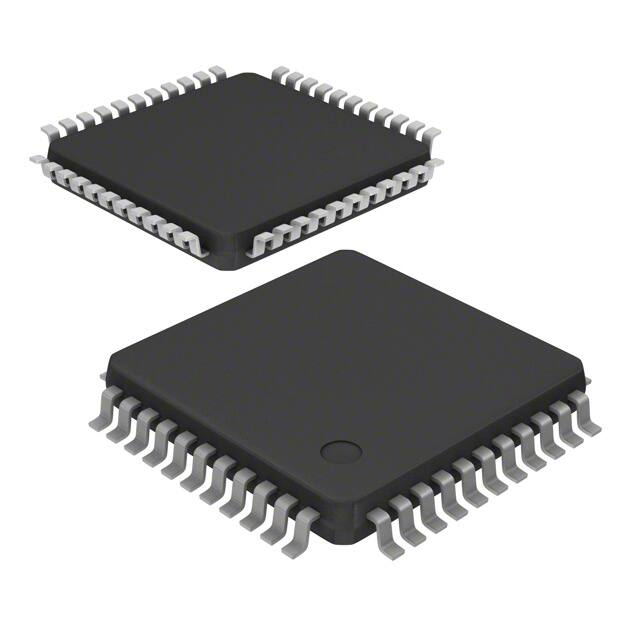


 工商网监
湘ICP备2023018690号
工商网监
湘ICP备2023018690号
