Product User Guide
ZAURA™ RF Wireless
Modules
PUG003003-1011
Introduction
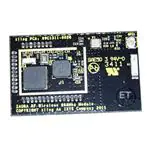
Zilog’s ZAURA RF Wireless Module is a cost-effective high-performance radio system
on a module designed for the wireless transmission of digital information. It is available in
both the 868 MHz and 915 MHz radio frequency bands.
The Module can be easily mounted on a two-layer PCB with minimal external connections.
It is a small-footprint (1.61" by 1.02") wireless modular system that can be designed into any
number of monitoring and control applications to enable wireless control. This Product User
Guide document discusses its specifications, lists schematics and software commands, and
provides a procedure for quickly getting started with development.
The Module, shown in Figure 1 mounted on a ZAURA RF Wireless Development Board
with its protective shield removed, delivers raw data at a rate of 50 kbits per second.
Figure 1. ZAURA RF Wireless Module and Development Board, shown without shield
PUG003003-1011
Page 1 of 19
�ZAURA™ RF Wireless Modules
Product User Guide
Module Features
The ZAURA RF Wireless Modules are shipped preloaded with a demo program which
includes a command line interpreter for control of the ZAURA RF Wireless Modules via the
UART. For details, see the ZAURA RF Wireless Module Shell User Manual (UM0235).
The ZAURA RF Wireless Module features many interface options, including:
•
2 four-wire UART ports (UART 0 is used by the ZAURA RF Shell Library if included
in the project)
•
I2C Controller
•
27 general-purpose port pins (21 available when using the ZAURA RF Shell Library,
25 available when the ZAURA RF Shell Library is not used)
•
8-channel 10-bit ADC
Top- and side-view dimensions of the Module are shown in Figures 2 and 3.
Figure 2. ZAURA RF Wireless Module Dimensions, Top View
Figure 3. ZAURA RF Wireless Module Dimensions, Side View
Note: Figures 2 and 3 refer to the 868 MHz Module but are identical for the 915 MHz
Module.
PUG003003-1011
Page 2 of 19
�ZAURA™ RF Wireless Modules
Product User Guide
The Module is shipped as a development kit which facilitates quick testing and development with the Module. This development system, with interfaces labeled in Figures 4 and
5, consists of a ZAURA RF Wireless Module mounted to a ZAURA RF Wireless Development Board that includes a USB Mini-B connector, user buttons and LEDs. The Development Board supports battery operation for portable testing, using two AA batteries.
USB Mini-B
Connector
SW2 CTS0–
LED D2
ZAURA RF
Wireless Module
SW1
SW4
LED D3
J3
J5
LED D1
Figure 4. ZAURA RF Wireless Module and Development Board, Top View
PUG003003-1011
Page 3 of 19
�ZAURA™ RF Wireless Modules
Product User Guide
AA Battery Holder
Figure 5. ZAURA RF Wireless Module and Development Board, Bottom View
Lastly, the ZAURA RF Wireless 868MHz Module is controlled by Zilog’s Z8F2480
MCU, which is based on the Z8 Encore! XP® CPU architecture. The Module’s RF transceiver is the Semtech SX1211, for which a full data sheet can be found at
www.semtech.com. For further details about the Z8F2480 MCU, please refer to the Z8
Encore! XP F1680 Series Product Specification (PS0250) on www.zilog.com.
Kit Contents
Each ZAURA RF Wireless Module Development Kit contains the following items:
•
Two (2) ZAURA RF Wireless Modules
•
Two (2) ZAURA RF Wireless Development Boards
•
Two (2) USB Mini-B to Type A cables
•
Four (4) AA batteries
All documentation and files can be downloaded from the Zilog website.
PUG003003-1011
Page 4 of 19
�ZAURA™ RF Wireless Modules
Product User Guide
Module Pin Description
Table 1 describes the functions of each of the ZAURA RF Wireless Module’s 41 pins.
Table 1. ZAURA RF Wireless Module Pin-Out
Pin #
Pin Name
Digital/
Analog
Details
I/O
1
PE6/T4CHD
D
Port Pin E6 or Timer 4 Channel D.
I/O
2
PE0/T4IN
D
Port Pin E0 or Timer 4 In.
I
3
VCC_3.3 V
A
Power, 3.3 V.
4
PA0/T0IN/T0OUT–/XIN
D
Port Pin A0 or XIN can be used to connect external
crystal Up to 20 MHz.
I/O
5
PA1/T0OUT/XOUT
D
Port Pin A1 or XOUT can be used to connect external
crystal, up to 20 MHz.
I/O
6
GND
A
Power, GND.
7
GND
A
Power, GND.
8
NC
9
PE1/SCL
D
Port Pin E1 or I2C Clock.
2
I/O
10
PE2/SDA
D
Port Pin E2 or I C Data.
I/O
11
PD7/COUT0
D
Port Pin D7 or Comparator out.
I/O
12
PE3/T4CHA/CTS0–
D
Port Pin E3 or Timer 4 Channel A or CTS0–.
I/O
13
PD6/DE1
D
Port Pin D6 or Driver Enable 1.
I/O
14
PA4/RXD0
D
Port Pin A4 or UART0 RXD0.
I/O
15
PA5/TXD0
D
Port Pin A5 or UART0 TXD0.
I/O
16
PD5/TXD1
D
Port Pin D5 or UART1 TXD1.
I/O
17
PA6/T1IN/T1OUT–
D
Port Pin A6 or Timer 1 In/Out.
I/O
18
PA7/T1OUT
D
Port Pin A7 or Timer 1 Out.
I/O
19
PD4/RXD1
D
Port Pin D4 or UART1 RXD1.
I/O
20
VCC_3.3 V
A
Power, 3.3 V.
21
PD0/RESET–
D
Port Pin D0 or Reset; input.
I/O
22
DBG
D
Debug input; connection for Zilog Debug Interface.
I/O
23
PD3/CTS1–
D
Port Pin D3 or UART1 CTS1.
I/O
24
GND
A
Power, GND.
25
PE4/T4CHB/RTS0–
D
Port Pin E4 or Timer 4 Channel D.
I/O
26
PD2/C1INP
D/A
Port Pin D2 or Comparator in P.
I/O
27
PD1/C1INN
D
Port Pin D1 or Comparator in N.
I/O
28
PB0/AMPOUT/ANA0
D
Port Pin B0.
I/O
29
PB1/AMPINN/ANA1
D/A
Port Pin B1 or Amp In N or Analog 1.
I/O
30
PB2/AMPINP/ANA2
D/A
Port Pin B2 or Amp In P or Analog 2.
I/O
PUG003003-1011
Page 5 of 19
�ZAURA™ RF Wireless Modules
Product User Guide
Table 1. ZAURA RF Wireless Module Pin-Out (Continued)
Pin #
Pin Name
Digital/
Analog
Details
I/O
31
PB4/ANA7
D/A
Port Pin B4 or Analog in 7.
I/O
32
PB5/VREF
D/A
Port Pin B5 or External Reference Voltage for ADC; not I/O
to exceed VCC.
33
PB3/CLKIN/ANA3
D/A
Port Pin B3 or Clock Input or Analog 3.
I/O
34
PE5/T4CHC
D
Port Pin E5 or Timer input.
I/O
PUG003003-1011
Page 6 of 19
�ZAURA™ RF Wireless Modules
Product User Guide
Module Specifications
The ZAURA RF Wireless Module operates within the frequency, current, voltage and
temperature specifications listed in Table 2.
Table 2. ZAURA RF Wireless Module Specifications
Frequency band:
Channel
0
1
2
3
Frequency band:
Channel
0
1
2
3
4
5
6
7
8
9
10
11
12
13
14
15
16
17
18
19
20
21
22
23
24
Receive current:
Transmit current:
Supply voltage:
Operating temperature range:
PUG003003-1011
868 MHz (range: 863–870 MHz)
Center Frequencies (MHz)
865.6
866.2
866.8
867.4
915 MHz (range: 902–928 MHz)
Center Frequencies (MHz)
903.0
904.0
905.0
906.0
907.0
908.0
909.0
910.0
911.0
912.0
913.0
914.0
915.0
916.0
917.0
918.0
919.0
920.0
921.0
922.0
923.0
924.0
925.0
926.0
927.0
6 mA @ 11 MHz and 3 V
30 mA @ 11 MHz and 3 V
2.1 V–3.6 V
0°C–70°C
Page 7 of 19
�ZAURA™ RF Wireless Modules
Product User Guide
The ZAURA RF Wireless Modules Development Kits ship with Zilog’s ad-hoc peer-topeer software loaded into the Z8F2480 microcontroller’s Flash memory. An example project, also included, allows users to investigate custom options. When combined with the
Zilog Developer Studio Integrated Development Environment (ZDS II IDE) and debug
tools, available from Zilog, developers can make changes to user source code which is
included with the software project.
Software Operation
Developing with the ZAURA RF Wireless Modules requires a PC running a serial terminal program; for purposes of demonstration, HyperTerminal is discussed in this document.
To get started, observe the following brief procedure.
1. Install two AA batteries on the reverse side of the development board and slide switch
SW3 to the BAT PWR ON position. Alternatively, when used with the USB interface,
power can be supplied from the USB port if SW3 is set to the USB PWR ON position.
2. Connect a USB Mini-B to Type A cable between the ZAURA RF Wireless Module
and a PC running Microsoft Windows (Zilog recommends Windows 7). The PC will
begin to enumerate the USB device and should automatically download the
appropriate PC software from the Internet. This software allows the ZAURA RF
Wireless Module’s USB interface to be used as a virtual COM (serial) port on the PC.
After this software has been installed, note the port number of the new (virtual) COM
port that has been added to the system.
3. To send commands to the Module, configure HyperTerminal for 57,600 bits per
second, 8 data bits, no parity, 1 stop bit and hardware flow control. It is necessary to
configure HyperTerminal to use the virtual COM port added to the system in the
previous step. By default, the ZAURA RF Shell Library does not echo typed
characters back to the console. To see typed characters, it is therefore necessary to
either configure HyperTerminal to enable Local Echo, to issue the uecho on console
command, or to rebuild the project with the ZAURA_RF_UartEcho configuration
variable set to TRUE in the ..\Conf\ZAURA_RF_Conf.c configuration file.
4. Apply power. A user prompt should appear on the terminal. If the prompt does not
appear, press the Enter key a few times in HyperTerminal. If the prompt still does not
appear, slide SW3 to the opposite position and then back to its original position.
Note: When the USB cable is disconnected and reconnected from the ZAURA RF Wireless Module, it is necessary to restart HyperTerminal so it recognizes that the virtual COM port is present.
Refer to the ZAURA RF Wireless Module Shell User Manual (UM0235) for command
details.
PUG003003-1011
Page 8 of 19
�ZAURA™ RF Wireless Modules
Product User Guide
Demonstration Project
The ZAURA RF Wireless Module demonstration project shows how to develop wireless
applications using the ZAURA RF and Shell libraries. These libraries contain the components indicated in Table 3.
Table 3. ZAURA RF Wireless Module Library Components
Library
Use
ZAURA_RF_866p5_MHz.lib
An RF library for the 863 to 870 MHz ISM band.
ZAURA_RF_915_MHz.lib
An RF library for the 902 to 928 MHz ISM band.
ZAURA_RF_Shell.lib
A command line interpreter and sample commands for use with either of
the above libraries. It is an interactive console used primarily to develop
new applications.
No_Shell.lib
A stub library to use in place of the Shell library for embedded
applications.
Set Up the Hardware
1. Connect the development board to a PC using a USB Mini-B to Type A cable.
2. Launch HyperTerminal on the PC.
3. Configure HyperTerminal for 57,600 bits per second, 8 data bits, no parity, 1 stop bit
and, optionally, with hardware flow control enabled. By default, the ZAURA RF Shell
Library does not echo typed characters back to the console. To see typed characters, it
is therefore necessary to either configure HyperTerminal to enable Local Echo, to
issue the uecho on console command, or to rebuild the project with the
ZAURA_RF_UartEcho configuration variable set to TRUE in the
..\Conf\ZAURA_RF_Conf.c configuration file.
4. Ensure the following settings:
a. SW3 is set to either USB PWR ON if not using batteries, or BAT PWR ON if two
AA batteries have been installed.
b. Jumpers J3 and J5 are in place.
Build the Project
1. The ZAURA RF Wireless Library is contained in a zip file labeled PUG0030SC01.zip; this file is downloadable free from the Zilog website. Extract the contents
of this zip file to an appropriate location on your hard drive.
2. Launch ZDS II, navigate to ..\ZAURA_RF_Wireless_vX.XXy\Demo and open the
ZAURA_RF_Demo.zdsproj project file, which is located inside the Demo folder.
PUG003003-1011
Page 9 of 19
�ZAURA™ RF Wireless Modules
Product User Guide
Note: vX.XXy refers to the version of the ZAURA RF software that was downloaded in
Step 1.
3. In the Build Configuration window, select either the 866p5_MHz build option or the
915_MHz build option based on the frequency band of the Module you are using.
4. Next, select the Build → Rebuild All menu option.
5. Download the project using the Tools → Flash Loader option or the Debug → Go
menu option.
Note: Some functions of the Demo project will place the Z8F2480 MCU into Stop
Mode, which will terminate the debug session.
Run the Demo without a Terminal
When power is initially applied to the ZAURA RF Wireless Module and its development
board, LED D1 and LED D2 will each illuminate. After initialization completes, LED D1
is extinguished and LED D2 remains illuminated.
Red LED D2 illuminates to indicate that the ZAURA_RF_Demo firmware is running and
the radio is in Receive Mode. When SW1 is pressed, the state of LED D1 on the (local)
ZAURA RF Wireless Development Board is toggled and a broadcast message is transmitted to other ZAURA RF Wireless modules. Modules within radio range of the transmitter
that receive the broadcast will configure LED D1 on their development boards to match
the state of LED D1 on the transmitter. Nodes that do not receive the broadcast will not
change the state of LED D1 on their development boards. For example, if LED D1 is initially OFF and SW1 is pressed, LED D1 is illuminated on that node and a broadcast message is transmitted, directing other ZAURA RF modules to illuminate LED D1 on their
development boards. Any modules that do not receive the broadcast will not alter the state
of LED D1 on their development boards.
If SW2 is pressed, both red LEDs D1 and D2 turn OFF, indicating that the ZAURA RF
Wireless Module is in a low power state and is unable to communicate with other nodes. If
SW1 is pressed while the Module is in the low power state, the unit is returned to Active
Mode, LED D2 illuminates, and the radio is placed into Receive Mode.
Run the Demo with a Terminal
When the ZAURA RF Wireless Module is used with a USB Mini-B to Type A cable connected to a PC running HyperTerminal, the operator can use the interactive console to
send and receive arbitrary packets in response to commands entered on the console.
For example, in the console display that follows, the operator sends the message, "Hello
world" to a specific Module, changes the Module’s station address and manipulates a
GPIO port pin on the remote station.
PUG003003-1011
Page 10 of 19
�ZAURA™ RF Wireless Modules
Product User Guide
ZAURA RF Wireless v1.10a Build 11081801
--------------------------------------FW checksum 7C57
>tx 56 "Hello world"
Transmit DA 56 Data: Hello world
Done transmit
>remote addr
local address: 56
>remote addr F7
>remote port e ^ 20
Port_E initially 20 now 00
For more information about developing an application using the ZAURA RF Wireless
Module libraries, please refer to the ZAURA RF Wireless Module Reference Manual
(RM0060), available on www.zilog.com.
PUG003003-1011
Page 11 of 19
�ZAURA™ RF Wireless Modules
Product User Guide
Appendix A. Schematic Diagrams
Figures 6 and 7 display schematic representations of the ZAURA RF Wireless Development Board.
FOOTPRINT FOR THE MODULE
P1
J12
1
2
3
4
5
6
7
8
1x8
PE6/T4CHD
PE0/T4IN
VCC_3v3_T
PA0/T0IN/T0OUT-/XIN
PA1/T0OUT/XOUT
GND
GND
1
2
3
4
5
6
7
8
ZAURA RF LEFT
J2
PE5/T4CHC
PB3/CLKIN/ANA3
PB5/VREF
PB4/ANA7
PB2/AMPINP/ANA2
PB1/AMPINN/ANA1
PB0/AMPOUT/ANA0
PD1/C1INN
PD2/C1INP
PE4/T4CHB
RTS0GND
PD3/CTS1DBG
PD0/RESETVCC_3v3_T
1
2
3
4
5
6
7
8
9
10
11
12
13
14
15
VCC_3v3_T
Test Points
J3
HDR/PIN 1x2
R1
10K
R2
10K
1
2
P3
34
33
32
31
30
29
28
27
26
25
24
23
22
21
20
1
PD2/C1INP
2
SW1
KSR211GLFS
HDR/PIN 1x15
ZAURA RF RIGHT
Test Points
ZAURA RF BOTTOM
9
10
11
12
13
14
15
16
17
18
19
2
1
2
SW2
KSR211GLFS
RTS-
HDR/PIN 1x2
J5
DBG
nRST
R3
D1
PE5/T4CHC 1
470
R4
RXD0
TXD0
D2
PE6/T4CHD 1
2
RED
RXD
VCC_3v3_T
2
RED
CTS0-
1
PD1/C1INN
PE1/SCL
PE2/SDA
PD7/COUT0
PE3/T4CHA
PD6/DE1
PA4/RXD0
PA5/TXD0
PD5/TXD1
PA6/T1IN/T1OUTPA7/T1OUT
PD4/RXD1
P2
470
TXD
1
2
3
4
5
6
7
8
9
10
11
CTS-
J7
HDR/PIN 1x11
Test Points
Figure 6. ZAURA RF Wireless Development Board, #1 of 2
PUG003003-1011
Zil
C fid ti l All Ri ht R
d
Page 12 of 19
�ZAURA™ RF Wireless Modules
Product User Guide
VCC_5V
U2
1
2
C4
C3
6
L1
FERRITE BEAD
4.7uF
R9
20K
0.1uF
R10
4.75K
Vin
Vout
GND
GND
EN
NC
3
5
4
C5
NCP582LXV33T2G
42 OHM
C6
4.7uF
0.1uF
GND
GND
P6
6
7
8
9
SH1
SH2
SH3
SH4
1
2
3
4
5
VBUS
DM
DP
ID
GND
U1
4
20
VCCIO
TXD
VCC
RXD
C1
USB-OTG, mini-AB
16
0.01uF
15
RTS
USBDM
CTS
USBDP
DTR
8
R8
19
100K 0.1W, 1%
24
27
GND
28
17
NC1
DSR
RESET
DCD
NC
RI
OSCI
CBUS0
OSCO
CBUS1
CBUS2
3v3 OUT
GND3
GND2
GND1
TEST
26
21
18
7
25
0.1uF
AGND
CBUS3
C2
CBUS4
1
RXD
5
BATT
TXD
3
CTS-
11
VCC_3v3_T
SW3
1
2
RTS-
3
2
POWER ON
EG1218
9
USB
10
6
23
U3
22
C7
1
C8
13
0.1uF
2
Holder 2xAA
3
VCC
FT232RL
DBG
GND
GND
2
IN
5
R11
20K
4.7uF
14
12
OUT
GND
OC
EN
4
TPS2051B
1
D3
nRST
R12
1
2
VCC_3v3
VCC_3v3_T
BH1
RED
100 ohm
GND
GND
R6
10K
R7
10K
Zilog Confidential All Rights Reserv
Zilog
P5
nRST
DBG
2
4
6
1
3
5
6800 Santa Teresa Blvd
San Jose, CA 95119
408-513-1500
Website: www.zilog.com
Title
ZAURA RF Wireless Module Evaluation Board
HDR/PIN 2x3
Page
GND
UNCONTROLLED WHEN PRINTED UNLESS STAMPED 'CONTROLLED COPY' IN RED BY DOCUMENT CONTROL
Size
B
Power and Interfaces
Document Number
96C1313-001G
Figure 7. ZAURA RF Wireless Development Board, #2 of 2
PUG003003-1011
Page 13 of 19
�ZAURA™ RF Wireless Modules
Product User Guide
Figures 8 and 9 display schematics of the ZAURA RF Wireless 868 MHz Module.
MOSI
MOSI
SCK
SCK
DATA
IRQ_0
CLKOUT
testpoint
IRQ_1
IRQ_1
VCC_3v3
RF INTERFACE
J1
1
IRQ_0
PLL_L
PLL_L
C18
RFIO
1
NC
TEST7
NSS_DAT-
14
NSS_CON-
MISO
NSS_DATNSS_CON-
3
12
4
13
11
Y1
12.8MHZ
10
9
2
18
17
SCK
CLKOUT
MOSI
20
19
21
DATA
IRQ_0
23
22
IRQ_1
PLL_LOCK
XTAL_P
MISO
1
32
L5
7.5nH
TEST4
TEST6
31
XTAL_M
LF_P
R28
1 ohm
TEST0
VR_PA
16
15
8
30
VR_DIG
7
29
TEST8
LF_M
47nF
VR_1V
6
28
VCO_P
L4
100nH
VCO_M
C25
5
0.22uF
NSS_CONFIG
4
1uF
27
VR_VCO
C20
MISO
VDD
TEST1
C28
U2
SX1211
NSS_DATA
3
26
TEST3
TEST5
25
01
2
01
TEST2
24
10uF
C23
C24
22PF
2.2PF
IN
2
C32
F1
B3717
680PF
C29
OUT
GND
GND2
GND3
GND4
5
1
3
4
6
10nF
R30
0 ohm
C26
R29
6.8K
C33
L1
8.2nH
0.1uF
L2
8.2nH
3.9PF
L6
18nH
DO NOT INSTALL
changed to
3.3pF
C34
DO NOT INSTALL
R31
RFC1
0.3PF
0 ohm
R32
0 ohm
3
2
1
A1
868MHZ/AT43B JOHANSON
2
NC
FP
1
ULTRA-MINI COAXIAL CONNECTOR
Zilog Con
Zilog
6800 Santa Te
San Jose, CA
408-513-1500
Website: www.
Title
ZAUR
Page
Size
SX12
D
Figure 8. ZAURA RF Wireless 868 MHz Module, #1 of 2
PUG003003-1011
Page 14 of 19
�VCC_3v3
PE0/T4IN
PE6/T4CHD
GND
PA1/T0OUT/XOUT
PA0/T0IN/T0OUT-/XIN
PD7/COUT0
PE2/SDA
PE1/SCL
ZAURA™ RF Wireless Modules
Product User Guide
Y2
32.768KHZ
C36
CTS0PD6/DE1
RXD0
PA4/RXD0
TXD0
PA5/TXD0
PD5/TXD1
PA6/T1IN/T1OUTPC4
PC5
PA7/T1OUT
1
2
3
4
5
6
7
8
9
10
11
PA2/DE0/X2IN
PA3/CTS0/X2OUT
PE3/T4CHA
PD6/DE1
PA4/RXD0/IRRX0
PA5/TXD0/IRTX0
PD5/TXD1/IRTX1
PA6/T1IN/T1OUT
PC4/MOSI/LED
PC5/SCK/LED
PA7/T1OUT
Z8F2480_44QFN
PC4
MOSI
PC5
SCK
PC2
NSS_DAT-
PC7
PE5/T4CHC
PB3/CLKIN/ANA3
PB5/VREF
PB4/ANA7
PB2/AMPINP/ANA2
PB1/AMPINN/ANA1
PB0/AMPOUT/ANA0
PD1/C1INN
PD2/C1INP
PC3/MISO/LED
PC2/SS/ANA6/LED
33
32
31
30
29
28
27
26
25
24
23
PE5/T4CHC
PB3/CLKIN/ANA3
PB5/VREF
PB4/ANA7
PB2/AMPINP/ANA2
PB1/AMPINN/ANA1
PB0/AMPOUT/ANA0
PD1/C1INN
PD2/C1INP
PC3
PC2
NSS_CON-
PC0
IRQ_0
PC1
IRQ_1
PC6
PLL_L
PC3
MISO
12
13
14
15
16
17
18
19
20
21
22
18pF
PA2
PA3
PE3/T4CHA
PD7/COUT0
PE2/SDA
PE1/SCL
AVSS
VSS
PA1/T0OUT/XOUT
PA0/T0IN/T0OUT/XIN
VDD
AVDD
PE0/T4IN
PE6/T4CHD
18pF
PD4/RXD1/IRRX1
PC6/T2IN/T2OUT/LED
PC7/T2OUT/LED
VDD
PD0/RESET
DBG
PD3/CTS1/COUT1
VSS
PE4/T4CHB
PC0/ANA4/C0INP/LED
PC1/ANA5/C0INN/LED
C35
44
43
42
41
40
39
38
37
36
35
34
RF INTERFACE
U14
PE6/T4CHD
PE0/T4IN
VCC_3v3
PA0/T0IN/T0OUT-/XIN
PA1/T0OUT/XOUT
GND
GND
ZAURA RF LEFT
0.1uF
PE1/SCL
PE2/SDA
PD7/COUT0
CTS0PD6/DE1
RXD0
TXD0
PD5/TXD1
PA6/T1IN/T1OUTPA7/T1OUT
PD4/RXD1
C30
1
2
3
4
5
6
7
8
1
2
3
4
5
6
7
8
9
10
11
GND
RTS0
PC6
PC7
VCC_3v3
PD0/RESETDBG
PD3/CTS1-
PD4/RXD1
VCC_3v3
PE4/T4CHB
PC0
PC1
P3
P1
P2
ZAURA RF BOTTOM
PE5/T4CHC
PB3/CLKIN/ANA3
PB5/VREF
PB4/ANA7
PB2/AMPINP/ANA2
PB1/AMPINN/ANA1
PB0/AMPOUT/ANA0
PD1/C1INN
PD2/C1INP
RTS0
GND
PD3/CTS1DBG
PD0/RESETVCC_3v3
1
2
3
4
5
6
7
8
9
10
11
12
13
14
15
ZAURA RF RIGHT
Figure 9. ZAURA RF Wireless 868 MHz Module, #2 of 2
PUG003003-1011
Page 15 of 19
�ZAURA™ RF Wireless Modules
Product User Guide
VCC_3v3
PE0/T4IN
PE6/T4CHD
GND
PA1/T0OUT/XOUT
PA0/T0IN/T0OUT-/XIN
PD7/COUT0
PE2/SDA
PE1/SCL
Figures 10 and 11 display schematics of the ZAURA RF Wireless 915 MHz Module.
PA2/DE0/X2IN
PA3/CTS0/X2OUT
PE3/T4CHA
PD6/DE1
PA4/RXD0/IRRX0
PA5/TXD0/IRTX0
PD5/TXD1/IRTX1
PA6/T1IN/T1OUT
PC4/MOSI/LED
PC5/SCK/LED
PA7/T1OUT
Z8F2480_44QFN
MOSI
PC5
SCK
PC2
NSS_DAT-
PC7
PE5/T4CHC
PB3/CLKIN/ANA3
PB5/VREF
PB4/ANA7
PB2/AMPINP/ANA2
PB1/AMPINN/ANA1
PB0/AMPOUT/ANA0
PD1/C1INN
PD2/C1INP
PC3/MISO/LED
PC2/SS/ANA6/LED
33
32
31
30
29
28
27
26
25
24
23
PE5/T4CHC
PB3/CLKIN/ANA3
PB5/VREF
PB4/ANA7
PB2/AMPINP/ANA2
PB1/AMPINN/ANA1
PB0/AMPOUT/ANA0
PD1/C1INN
PD2/C1INP
PC3
PC2
NSS_CON-
PC0
IRQ_0
PC1
IRQ_1
PC6
PLL_L
PC3
MISO
P3
P1
1
2
3
4
5
6
7
8
PE6/T4CHD
PE0/T4IN
VCC_3v3
PA0/T0IN/T0OUT-/XIN
PA1/T0OUT/XOUT
GND
GND
ZAURA RF Left
PE1/SCL
PE2/SDA
PD7/COUT0
CTS0PD6/DE1
RXD0
TXD0
PD5/TXD1
PA6/T1IN/T1OUTPA7/T1OUT
PD4/RXD1
GND
RTS0
PC6
PC7
VCC_3v3
PD0/RESETDBG
PD3/CTS1-
PD4/RXD1
VCC_3v3
PE4/T4CHB
PC0
PC1
12
13
14
15
16
17
18
19
20
21
22
18pF
CTS0PD6/DE1
RXD0
PA4/RXD0
TXD0
PA5/TXD0
PD5/TXD1
PA6/T1IN/T1OUTPC4
PC5
PA7/T1OUT
1
2
3
4
5
6
7
8
9
10
11
PC4
C30
0.1uF
P2
PE5/T4CHC
PB3/CLKIN/ANA3
PB5/VREF
PB4/ANA7
PB2/AMPINP/ANA2
PB1/AMPINN/ANA1
PB0/AMPOUT/ANA0
PD1/C1INN
PD2/C1INP
RTS0
GND
PD3/CTS1DBG
PD0/RESETVCC_3v3
1
2
3
4
5
6
7
8
9
10
11
12
13
14
15
ZAURA RF Right
1
2
3
4
5
6
7
8
9
10
11
Y2
32.768KHZ
C36
PA2
PA3
PE3/T4CHA
PD7/COUT0
PE2/SDA
PE1/SCL
AVSS
VSS
PA1/T0OUT/XOUT
PA0/T0IN/T0OUT/XIN
VDD
AVDD
PE0/T4IN
PE6/T4CHD
18pF
PD4/RXD1/IRRX1
PC6/T2IN/T2OUT/LED
PC7/T2OUT/LED
VDD
PD0/RESET
DBG
PD3/CTS1/COUT1
VSS
PE4/T4CHB
PC0/ANA4/C0INP/LED
PC1/ANA5/C0INN/LED
C35
44
43
42
41
40
39
38
37
36
35
34
RF INTERFACE
U14
ZAURA RF bottom
Figure 10. ZAURA RF Wireless 915 MHz Module, #1 of 2
PUG003003-1011
Page 16 of 19
�ZAURA™ RF Wireless Modules
Product User Guide
MOSI
SCK
IRQ_0
IRQ_1
RF INTERFACE
VCC_3v3
PLL_L
MOSI
SCK
DATA
J1
IRQ_0
1
CLKOUT
IRQ_1
Test Point place holder
PLL_L
C18
RFIO
1
NC
TEST7
NSS_DAT-
14
NSS_CON-
MISO
NSS_DATNSS_CON-
3
12
4
13
11
Y1
12.8MHZ
10
9
2
XTAL_P
MISO
1
18
17
SCK
MOSI
20
19
DATA
CLKOUT
23
21
IRQ_0
IRQ_1
PLL_LOCK
TEST4
TEST6
32
L5
7.5nH
XTAL_M
LF_P
31
1 ohm
TEST0
VR_PA
16
15
8
30
7
29
TEST8
VR_DIG
LF_M
100nH
R28
VR_1V
VCO_P
28
6
L4
VCO_M
47nF
NSS_CONFIG
5
0.22uF/220nF
MISO
VDD
4
1uF
27
VR_VCO
C25
U2
SX1211
NSS_DATA
3
C20
TEST2
24
C28
TEST3
TEST1
26
gnd
TEST5
25
2
01
22
10uF
C23
C24
22PF
C32
F1
B3588
680PF
OUT
GND
GND2
GND3
GND4
C29
R29
10nF
6.8K
5
1
3
4
6
IN
2
2.2PF
C33
R30
0 ohm
L7
0.1uF
L1
6.8nH
L2
6.8nH
4.7nH
DO NOT INSTALL
L6
10nH
changed to
3.3pF
C26
R31
0.5PF
0 ohm
DO NOT INSTALL
3
2
1
RFC1
A1
915Mhz JOHANSON
2
NC
FP
1
R32
0 ohm
ULTRA-MINI RECPT
Figure 11. ZAURA RF Wireless 915 MHz Module, #2 of 2
PUG003003-1011
Page 17 of 19
�ZAURA™ RF Wireless Modules
Product User Guide
Precharacterization Product
The product represented by this document is newly introduced and Zilog has not completed the full characterization of the product. The document states what Zilog knows
about this product at this time, but additional features or nonconformance with some
aspects of the document might be found, either by Zilog or its customers in the course of
further application and characterization work. In addition, Zilog cautions that delivery
might be uncertain at times, due to start-up yield issues.
Ordering Information
The ZAURA RF Wireless 868 MHz and 915 MHz Modules are each available as development kits, as listed in Table 4. Each kit includes two ZAURA RF Wireless Modules and
two ZAURA RF Wireless development boards. Both ZAURA RF Wireless Module
Development Kits can be ordered from the Zilog website using the part numbers listed in
Table 4. For more information about ordering, please consult your local Zilog Sales
Office. The Zilog website (www.zilog.com) lists all regional offices and provides additional information about ZAURA RF Wireless Technology products.
Table 4. ZAURA RF Wireless Module Ordering Information
Part Number
Description
ZAURA868100MODG
ZAURA RF Wireless 868 MHz Module
ZAURA915100MODG
ZAURA RF Wireless 915 MHz Module
ZAURA868100KITG
ZAURA RF Wireless 868 MHz Module Development Kit
ZAURA915100KITG
ZAURA RF Wireless 915 MHz Module Development Kit
Related Documentation
The documents associated with the ZAURA RF Wireless Modules are listed in Table 5
and can also be found on the Zilog website at www.zilog.com.
Table 5. ZAURA RF Wireless Module Documentation
Document
Number
Description
PUG0030
This ZAURA RF Wireless Module Reference Design document
PUG0030-SC01
ZAURA RF Wireless Library
UM0235
ZAURA RF Module Shell User Manual
RM0060
ZAURA RF Wireless Library Reference Manual
PUG003003-1011
Page 18 of 19
�ZAURA™ RF Wireless Modules
Product User Guide
Customer Support
To learn more about this product, find additional documentation, get your technical questions answered or report issues, please contact esales@zilog.com.
Warning:
DO NOT USE THIS PRODUCT IN LIFE SUPPORT SYSTEMS.
LIFE SUPPORT POLICY
ZILOG’S PRODUCTS ARE NOT AUTHORIZED FOR USE AS CRITICAL COMPONENTS IN LIFE
SUPPORT DEVICES OR SYSTEMS WITHOUT THE EXPRESS PRIOR WRITTEN APPROVAL OF
THE PRESIDENT AND GENERAL COUNSEL OF ZILOG CORPORATION.
As used herein
Life support devices or systems are devices which (a) are intended for surgical implant into the body, or (b)
support or sustain life and whose failure to perform when properly used in accordance with instructions for
use provided in the labeling can be reasonably expected to result in a significant injury to the user. A
critical component is any component in a life support device or system whose failure to perform can be
reasonably expected to cause the failure of the life support device or system or to affect its safety or
effectiveness.
Document Disclaimer
©2011 Zilog, Inc. All rights reserved. Information in this publication concerning the devices, applications,
or technology described is intended to suggest possible uses and may be superseded. ZILOG, INC. DOES
NOT ASSUME LIABILITY FOR OR PROVIDE A REPRESENTATION OF ACCURACY OF THE
INFORMATION, DEVICES, OR TECHNOLOGY DESCRIBED IN THIS DOCUMENT. ZILOG ALSO
DOES NOT ASSUME LIABILITY FOR INTELLECTUAL PROPERTY INFRINGEMENT RELATED
IN ANY MANNER TO USE OF INFORMATION, DEVICES, OR TECHNOLOGY DESCRIBED
HEREIN OR OTHERWISE. The information contained within this document has been verified according
to the general principles of electrical and mechanical engineering.
ZAURA and Z8 Encore! XP are trademarks or registered trademarks of Zilog, Inc. All other product or
service names are the property of their respective owners.
PUG003003-1011
Page 19 of 19
�


 工商网监
湘ICP备2023018690号
工商网监
湘ICP备2023018690号
