OB3332Bx
Single Winding, High PF Non-Isolated dimmable LED driver
GENERAL DESCRIPTION
FEATURES
OB3332Bx is a TRIAC dimmable high power factor,
highly integrated buck/buck-boost regulator with
advanced features to provide high efficiency
control and high precision constant current output
for dimmable LED lighting applications.
The proprietary CC control scheme is used to
provide features of insensitivity to inductance and
line voltage. Without external large compensation
capacitor, the system can achieve high power
factor with proprietary PFC control scheme.
OB3332Bx offers comprehensive protection
coverage with auto-recovery features including
LED open loop protection, LED short circuit
protection, cycle-by-cycle current limiting, built-in
leading edge blanking, VDD under voltage lockout
(UVLO), thermal foldback etc.
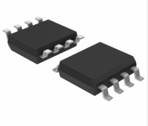
OB3332Bx is offered in SOP-8 package.
Excellent TRIAC dimming performance
Low system cost and high efficiency
High PF(PF>0.9)@175~264Vac input
Support buck/buck-boost topology
High precision constant current regulation at
universal AC input
Quasi-Resonant operation
Thermal foldback function for LED output
current control
Insensitivity to inductance and line voltage
variation
LED short circuit protection
LED open loop protection
Cycle-by-cycle current limiting
Built-in leading edge blanking (LEB)
VDD under voltage lockout with hysteresis
Over temperature protection (OTP)
APPLICATIONS
Dimmable LED lighting
TYPICAL APPLICATION
Figure 1 Buck Application circuit
Figure 2 Buck-Boost Application circuit
©On-Bright Electronics
Confidential
-1-
Datasheet
OB_DOC_DS_3332BxA4
�OB3332Bx
Single Winding, High PF Non-Isolated dimmable LED driver
GENERAL INFORMATION
Pin Configuration
The pin map is shown as below.
FB
1
8
DRAIN
GND
2
7
DRAIN
6
DRAIN
VDD
CS
3
4
5
Absolute Maximum Ratings
Parameter
VDD Voltage
CS Input Voltage
FB Input Voltage
OB3332BPCP-J
DRAIN
OB3332BMCP-H
Voltage
OB3332BNCP-H
OB3332BRCP-H
Min/Max Operating Junction
Temperature TJ
Operating
Ambient
Temperature TA
Min/Max Storage Temperature
Tstg
Lead Temperature (Soldering,
10secs)
DRAIN
Ordering Information
Part Number
Description
8 Pin SOP, Halogen-free in
OB3332BMCP-H
Tube
8 Pin SOP , Halogen-free in
OB3332BMCPA-H
T&R
8 Pin SOP, Halogen-free in
OB3332BNCP-H
Tube
8 Pin SOP , Halogen-free in
OB3332BNCPA-H
T&R
8 Pin SOP, Halogen-free in
OB3332BPCP-J
Tube
8 Pin SOP , Halogen-free in
OB3332BPCPA-J
T&R
8 Pin SOP, Halogen-free in
OB3332BRCP-H
Tube
8 Pin SOP , Halogen-free in
OB3332BRCPA-H
T&R
Note: All Devices are offered in Halogen-free Package if
Value
-0.3 to 20V
-0.3 to 7V
-0.3 to 7V
-0.3 to 500V
-0.3 to 650V
-40 to 150 ℃
-40 to 85 ℃
-55 to 150 ℃
260 ℃
Note: Stresses beyond those listed under “absolute maximum
ratings” may cause permanent damage to the device. These
are stress ratings only, functional operation of the device at
these or any other conditions beyond those indicated under
“recommended operating conditions” is not implied. Exposure
to absolute maximum-rated conditions for extended periods
may affect device reliability.
Output Power Table
not otherwise noted.
Product
Condition
175Vac~264Vac
Input
OB3332BMCP-H
Io≤80mA
10W
OB3332BNCP-H
Io≤105mA
12W
OB3332BPCP-J
Io≤180mA
17.6W
OB3332BRCP-H
Io≤220mA
18.5W
Note: Maximum practical continuous power in an open frame
design with sufficient drain pattern as a heat sink, at 50℃
ambient and 60℃ temperature rise. Higher output power is
possible with extra added heat sink 、 air circulation and
decrease output current to reduce thermal resistance.
Recommended Operating Condition
Symbol Parameter
Range
VDD
VDD Supply Voltage
8 to 16V
Package Dissipation Rating
Package
RθJA (℃/W)
SOP8
90
©On-Bright Electronics
Confidential
-2-
Datasheet
OB_DOC_DS_3332BxA4
�OB3332Bx
Single Winding, High PF Non-Isolated dimmable LED driver
Marking Information
YWWZZZ
OB3332MCP
YWWZZZ
OB3332NCP
B
B
s
s
Y: Year Code
Y: Year Code
WW: Week Code (01-52)
WW: Week Code (01-52)
ZZZ:Lot Code
ZZZ:Lot Code
C: SOP8
C: SOP8
P:Halogen-free Package
P:Halogen-free Package
B:Character Code
B:Character Code
S: Internal Code(Optional)
S: Internal Code(Optional)
YWWZZZ
OB3332PCP
YWWZZZ
OB3332RCP
B
B
s
s
Y: Year Code
Y: Year Code
WW: Week Code (01-52)
WW: Week Code (01-52)
ZZZ:Lot Code
ZZZ:Lot Code
C: SOP8
C: SOP8
P:Halogen-free Package
P:Halogen-free Package
B:Character Code
B:Character Code
S: Internal Code(Optional)
S: Internal Code(Optional)
TERMINAL ASSIGNMENTS
Pin Num
Pin Name
I/O
Description
1
FB
I/O
The voltage feedback from output. Connected to resistor divider from
output voltage.
2
GND
P
Power Ground.
3
VDD
P
Power supply input.
4
CS
I/O
Current sensing terminal.
5,6,7,8
DRAIN
I/O
Drain of power MOSFET.
©On-Bright Electronics
Confidential
-3-
Datasheet
OB_DOC_DS_3332BxA4
�
很抱歉,暂时无法提供与“OB3332BPCPA-J”相匹配的价格&库存,您可以联系我们找货
免费人工找货- 国内价格
- 1+1.96620
- 30+1.89840
- 100+1.76280
- 500+1.62720
- 1000+1.55940
