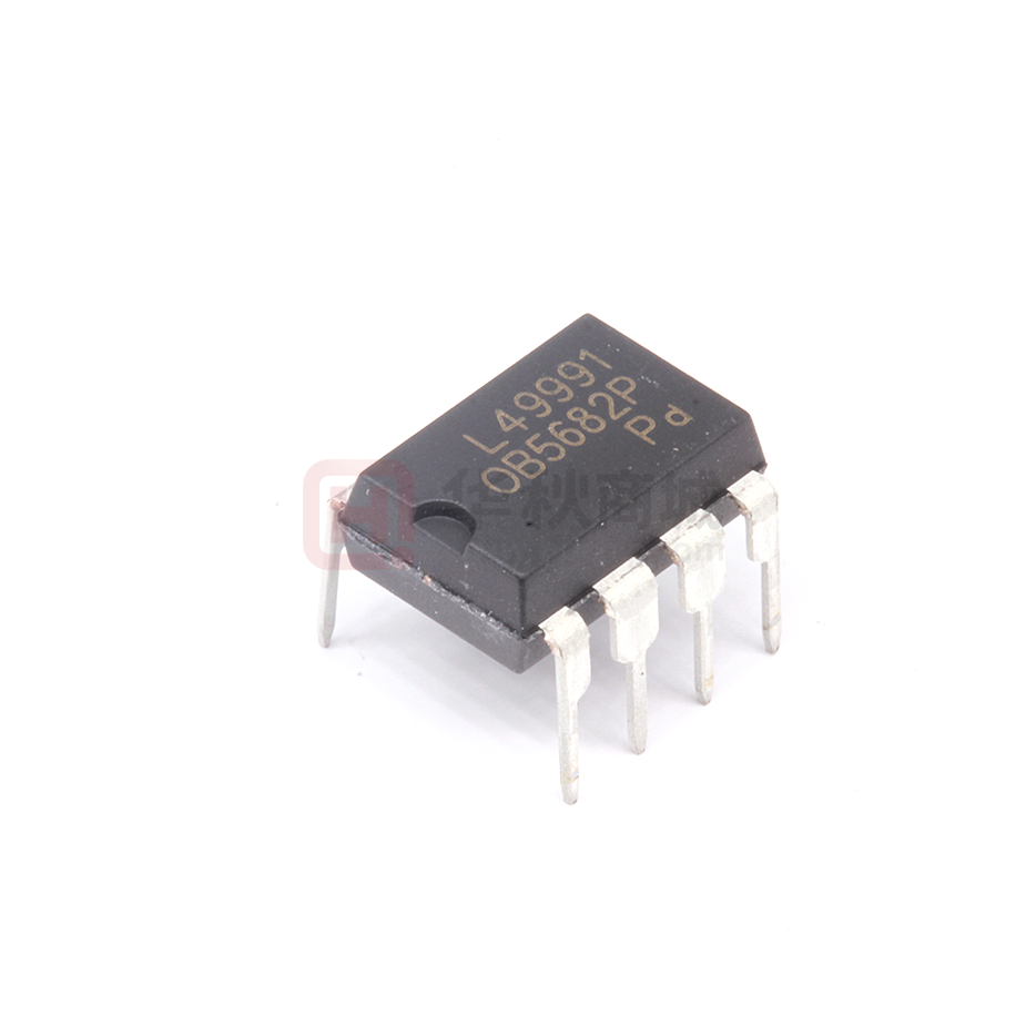
OB5682x
High Precision LED Off-line LED Power Switch
GENERAL DESCRIPTION
FEATURES
OB5682x is a primary side regulation off-line LED
lighting power switch which can achieve accurate
LED current. It significantly simplifies LED lighting
system design by eliminating the secondary side
feedback circuitry, HV startup resistor and power
supply capacitor.
LED current (CC control) can be adjusted by the
external sense resistor connected between CS pin
and ground.
OB5682x offers comprehensive protection
coverage with auto-recovery features including
LED open circuit protection, LED short circuit
protection, Cycle-by-Cycle current limiting, and
thermal foldback, etc.
HV startup without power supply capacitor
Low System Cost and High Efficiency
Low operation current
Primary-side Sensing and Regulation Without
TL431 and Opto-coupler
Cycle-by-Cycle Current Limiting
Built-in Leading Edge Blanking (LEB)
LED Short Circuit Protection
LED Open Circuit Protection
Thermal foldback
APPLICATIONS
OB5682x is offered in SOT33-5(A)/SOP7/DIP7
package.
LED lighting
TYPICAL APPLICATION
VLED
~
AC
NP
+
NS
+ CO
OB5682x
©On-Bright Electronics
HV
GND
OVP
CS
Drain
Confidential
-1-
Datasheet
OB_DOC_DS_5682xA2
�OB5682x
High Precision LED Off-line LED Power Switch
Power Switch
GENERAL INFORMATION
Pin Configuration
The pin map is shown as below for SOT33-5(A).
HV
1
GND
2
5
4
OVP
Package Dissipation Rating
Package
RθJA (℃/W)
SOT33-5(A)
145
SOP7
95
DIP7
77
CS
Absolute Maximum Ratings
Parameter
Drain Voltage
HV Voltage
CS Input Voltage
OVP Input Voltage
Min/Max Operating Junction
Temperature TJ
Operating
Ambient
Temperature TA
Min/Max Storage
Temperature Tstg
Lead Temperature
(Soldering, 10secs)
DRAIN
3
The pin map is shown as below for SOP7.
7
HV
1
NC
2
OVP
3
6
DRAIN
CS
4
5
DRAIN
GND
The pin map is shown as below for DIP7.
7
CS
3
6
DRAIN
4
5
DRAIN
HV
1
NC
2
GND
OVP
Value
-0.3 to BVdss
-0.3 to 650V
-0.3 to 8V
-0.3 to 8V
-40 to 150 ℃
-40 to 85 ℃
-55 to 150 ℃
260 ℃
Note: Stresses beyond those listed under “absolute maximum
ratings” may cause permanent damage to the device. These
are stress ratings only, functional operation of the device at
these or any other conditions beyond those indicated under
“recommended operating conditions” is not implied. Exposure
to absolute maximum-rated conditions for extended periods
may affect device reliability.
Ordering Information
Part Number
Description
SOT33-5(A), Halogen-free in
OB5682MMKP-H
T&R
OB5682NJP-H
SOP7, Halogen-free in Tube
OB5682NJPA-H
SOP7, Halogen-free in T&R
OB5682PJP
SOP7, Halogen-free in Tube
OB5682PJPA
SOP7, Halogen-free in T&R
OB5682PASP
DIP7, Halogen-free in Tube
OB5682TASP
DIP7, Halogen-free in Tube
Output Power Table
90~264Vac
Product
Input
OB5682MMKP-H 6W
OB5682NJP-H
9W
220Vac±20%
Input
10W
12W
OB5682PJP
12W
15W
OB5682PASP
14W
20W
OB5682TASP
16W
24W
Note: Maximum practical continuous power in an open frame
design with sufficient drain pattern as a heat sink, at 50℃
ambient and 60℃ temperature rise. Higher output power is
possible with extra added heat sink, air circulation and
decrease output current to reduce thermal resistance.
Marking Information
OB5682x
High Precision Off-line LED
Switch
X
Package
X
X
Package
Halogen-free
-
X
Packing
Bvdss
MK:SOT33-5(A) P:Halogen-free Blank:Tube Blank:600V
J:SOP7
H:650V
A:T&R
AS:DIP7
©On-Bright Electronics
Confidential
-2-
Datasheet
OB_DOC_DS_5682xA2
�OB5682x
High Precision LED Off-line LED Power Switch
Power Switch
YWWZZZ
OB5682N
Ps
682YWW
ZZZ s
Y: Year Code
WW: Week Code (01-52)
ZZZ:Lot Code
S: Internal Code(Optional)
YWWZZZ
OB5682P
Ps
Y: Year Code
Y: Year Code
WW: Week Code (01-52)
WW: Week Code (01-52)
ZZZ:Lot Code
ZZZ:Lot Code
P:Halogen-free Package
P:Halogen-free Package
S: Internal Code(Optional)
S: Internal Code(Optional)
YWWZZZ
OB5682T
Ps
YWWZZZ
OB5682P
Ps
Y: Year Code
Y: Year Code
WW: Week Code (01-52)
WW: Week Code (01-52)
ZZZ:Lot Code
ZZZ:Lot Code
P:Halogen-free Package
P:Halogen-free Package
s: Internal Code(Optional)
s: Internal Code(Optional)
TERMINAL ASSIGNMENTS for OB5682MMKP-H
Pin Num
1
2
3
4
5
Pin Name
HV
GND
OVP
Drain
CS
I/O
P
P
I
I
I
Description
High Voltage power supply
Ground
Over Voltage Protection configuration pin
Drain of internal MOSFET
Current sense pin
TERMINAL ASSIGNMENTS for OB5682NJP-H/ PJP
Pin Num
1
2
3
4
5,6
7
Pin Name
HV
NC
OVP
CS
Drain
GND
I/O
P
I
I
I
P
Description
High Voltage power supply
No connection
Over Voltage Protection configuration pin
Current sense pin
Drain of internal MOSFET
Ground
TERMINAL ASSIGNMENTS for OB5682PASP/ TASP
Pin Num
1
2
3
4
5,6
7
Pin Name
HV
NC
GND
OVP
Drain
CS
©On-Bright Electronics
I/O
P
P
I
I
I
Description
High Voltage power supply
No connection
Ground
Over Voltage Protection configuration pin
Drain of internal MOSFET
Current sense pin
Confidential
3
Datasheet
OB_DOC_DS_5682xA2
�OB5682x
High Precision LED Off-line LED Power Switch
Power Switch
BLOCK DIAGRAM
HV
UVLO
CC
Controller
OVP
LDO
Logic
Control
OVP
DRAIN
Gate
Driver
GND
©On-Bright Electronics
Thermal
foldback
OCP
Confidential
-4-
CS
Datasheet
OB_DOC_DS_5682xA2
�OB5682x
High Precision LED Off-line LED Power Switch
Power Switch
ELECTRICAL CHARACTERISTICS
(TA = 25℃if not otherwise noted)
Symbol
Parameter
Test Conditions
Min Typ.
Max Unit
Supply Voltage (VDD) Section
I_static
Static Current
HV=45V
200
uA
Current Sense Input Section
TLEB
Leading Edge Blanking time
0.4
us
Vth_ocp
Over current threshold
500
mV
Toff_max
Maximum off time
600
us
Ton_max
Maximum on time
50
us
Tdem_blk
Demag blanking time
2
us
Rovp=10Kohm
5
us
Rovp=floating
4.7
us
130
℃
OVP Section
Toff_min
Minimum off time
Thermal Section
Tthermal
Thermal regulation threshold
BVdss(V)
MOSFET Drain-Source Breakdown Voltage
Parameter
Product
OB5682MMKP-H
OB5682NJP-H
OB5682PJP
OB5682PASP
OB5682TASP
Min
650
650
600
600
600
Typ.
©On-Bright Electronics
Confidential
-5-
Max
Datasheet
OB_DOC_DS_5682xA2
�OB5682x
High Precision LED Off-line LED Power Switch
Power Switch
OPERATION DESCRIPTION
OB5682x is a cost effective PWM power switch
optimized for off-line LED lighting applications.
Based on flyback converter topology working in
DCM mode, it operates in primary side sensing
and regulation, It significantly simplifies the
LED lighting system design by eliminating the
secondary side feedback circuitry, HV startup
resistor
and power
supply capacitor.
Proprietary built-in CC control can achieve high
precision LED current meeting LED lighting
application requirements.
Where Vth_ocp is over current threshold, N is the
ratio of transformer between primary winding and
secondary winding.
Adjustable CC point and Output Power
In OB5682x, the CC point and maximum output
power can be externally adjusted by external
current sense resistor Rcs at CS pin as illustrated
in Typical Application Diagram. The output power
is adjusted through CC point change. The larger
Rcs, the smaller CC point is, and the smaller
output power becomes.
Start up Control
Operation switching frequency
The switching frequency of OB5682x is adaptively
controlled according to the load conditions and the
operation modes. No external frequency setting
components are required.
For flyback operating in DCM, The operation
frequency is given by
At work state, OB5682x gets power supply
directly from HV pin and regulates the supply
voltage by internal startup circuits.
Principle of CC Operation
To support OB5682x proprietary CC control,
system needs to be designed in DCM mode for
flyback system (Refer to Typical Application
Diagram on page1). The LED output current
ILED is given by:
1
𝐼𝐿𝐸𝐷 = 2 𝐿𝑃 . 𝐹𝑆𝑊 . 𝐼𝑃𝐾 2 /𝑉𝑂
𝐹𝑆𝑊 = 8 .
(1)
1
LED Short Circuit Protection
OB5682x detects the states of LED. When LED
string short circuit occurs, the switching frequency
is reduced to the minimum switching frequency
with maximum Toff time. OB5682x resumes
normal operation after the fault condition is
removed.
PWM Off
Programmable LED Open Circuit Protection /
OVP
The OB5682x provide programmable output over
voltage protection when LED string are open. The
threshold voltage of OVP is set by the minimum off
time (Toff_min), when the off time of OB5682x is
less then the Toff_min OB5682x stops switching
and re-detect the LED string status after 150ms
(typical). If the fault condition is removed,
OB5682x resumes normal operation. Otherwise,
the above operation is repeated. The minimum off
time (Toff_min) is given by
TDemag
TON
PWM On
Figure.1 Primary voltage waveform
Since Tdemag is direct proportional to the
inductance, as a result, the product of Lp and
Fsw is constant, thus output current will not
change as primary winding inductance
changes. The output LED current is
1
𝐼𝐿𝐸𝐷 = 4 𝑁
𝑉𝑡ℎ_𝑜𝑐𝑝
𝑅𝐶𝑆
©On-Bright Electronics
(4)
Current Sensing and Leading Edge Blanking
Cycle-by-Cycle current limiting is offered in
OB5682x. The switch current is detected by a
sense resistor into the CS pin. An internal leading
edge blanking circuit chops off the sensed voltage
spike at initial power MOSFET on state so that the
external RC filtering on sense input is no longer
needed.
(2)
𝑑𝑒𝑚𝑎𝑔
𝐿𝑝 . 𝐼𝐿𝐸𝐷
The switching frequency at maximum output
power is recommended 65kHz~75kHz, and the
minimum switching frequency at normal operation
should not below 30kHz.
Where Lp indicates the inductance of primary
winding, Ipk is the peak current of primary
winding.
Refer to the equation 1, the change of the
primary winding inductance results in the
change of the constant output current. To
compensate the change from variations of
primary winding inductance, the switching
frequency is locked by an internal loop such
that the switching frequency is
𝐹𝑆𝑊 = 2𝑇
𝑉𝑂 . 𝑁 2
𝑇𝑜𝑓𝑓_𝑚𝑖𝑛 =
(3)
Confidential
-6-
𝐿𝑃 .𝑉𝑡ℎ_𝑜𝑐𝑝
𝑁.𝑅𝐶𝑆 .𝑉𝑂𝑉𝑃
(5 )
Datasheet
OB_DOC_DS_5682xA2
�OB5682x
High Precision LED Off-line LED Power Switch
Power Switch
Where Vovp is threshold voltage of OVP.
A resistor Rovp is connected between the OVP
pin and ground. The minimum off time
(Toff_min) can be adjusting the resistance of
Rovp, the resistance is given by
𝑅𝑂𝑉𝑃 = 𝑇
0.05
𝑜𝑓𝑓_𝑚𝑖𝑛
Thermal foldback
OB5682x provides thermal foldback function to
control LED output current. The LED current will
reduce with the temperature rise up. When the
temperature is over 130 ℃ (typical), the output
current follows the thermal foldback function
scheme. When the temperature is below 130℃
(typical), the output current returns to the full level.
(6)
And the resistance range of Rovp should be
5K~16K for Toff_min setting.
When OVP pin floating, Toff_min is set to 4.7us
internally.
©On-Bright Electronics
Confidential
-7-
Datasheet
OB_DOC_DS_5682xA2
�OB5682x
High Precision LED Off-line LED Power Switch
Power Switch
PACKAGE MECHANICAL DATA
SOP7
Symbol
Dimensions In Millimeters
Dimensions In Inches
Min
Max
Min
Max
A
1.350
1.750
0.053
0.069
A1
0.050
0.250
0.002
0.010
A2
1.250
1.650
0.049
0.065
b
0.310
0.510
0.012
0.020
c
0.100
0.250
0.004
0.010
D
4.700
5.150
0.185
0.203
E
3.800
4.000
0.150
0.157
E1
5.800
6.200
0.228
0.244
e
1.270 (BSC)
0.050 (BSC)
L
0.400
1.270
0.016
0.050
θ
0º
8º
0º
8º
©On-Bright Electronics
Confidential
-8-
Datasheet
OB_DOC_DS_5682xA2
�OB5682x
High Precision LED Off-line LED Power Switch
Power Switch
SOT33-5(A)
Symbol
Dimensions In Millimeters
Dimensions In Inches
Min
Max
Min
Max
A
-
1.30
-
0.051
A1
0.05
0.15
0.002
0.006
A2
1.05
1.15
0.041
0.045
a
0.52
0.60
0.020
0.024
b
0.58
0.66
0.023
0.026
c
0.15
0.19
0.006
0.007
D
3.80
4.00
0.150
0.157
E1
2.50
2.70
0.098
0.106
E
3.80
4.20
0.150
0.165
e
0.90(BSC)
0.035(BSC)
e1
0.81(BSC)
0.032(BSC)
e2
1.25(BSC)
0.049(BSC)
L
0.40
0.60
0.016
0.024
θ
0º
8º
0º
8º
©On-Bright Electronics
Confidential
-9-
Datasheet
OB_DOC_DS_5682xA2
�OB5682x
High Precision LED Off-line LED Power Switch
Power Switch
DIP7
Symbol
A
A1
A2
B
B1
C
D
E
E1
e
L
E2
Dimensions In Millimeters
Min
Max
3.710
0.381
2.921
0.350
5.334
Dimensions In Inches
Min
Max
4.953
0.650
0.146
0.015
0.115
0.014
0.360
10.160
7.112
8.255
0.008
0.354
0.240
0.288
1.524 (BSC)
0.200
9.000
6.096
7.320
©On-Bright Electronics
0.195
0.026
0.06 (BSC)
2.540 (BSC)
2.921
7.620
0.210
0.014
0.400
0.280
0.325
0.1 (BSC)
3.810
10.920
Confidential
- 10 -
0.115
0.300
0.150
0.430
Datasheet
OB_DOC_DS_5682xA2
�OB5682x
High Precision LED Off-line LED Power Switch
Power Switch
IMPORTANT NOTICE
RIGHT TO MAKE CHANGES
On-Bright Electronics Corp. reserves the right to make corrections, modifications, enhancements,
improvements and other changes to its products and services at any time and to discontinue any product
or service without notice. Customers should obtain the latest relevant information before placing orders
and should verify that such information is current and complete.
WARRANTY INFORMATION
On-Bright Electronics Corp. warrants performance of its hardware products to the specifications applicable
at the time of sale in accordance with its standard warranty. Testing and other quality control techniques
are used to the extent it deems necessary to support this warranty. Except where mandated by
government requirements, testing of all parameters of each product is not necessarily performed.
On-Bright Electronics Corp. assumes no liability for application assistance or customer product design.
Customers are responsible for their products and applications using On-Bright’s components, data sheet
and application notes. To minimize the risks associated with customer products and applications,
customers should provide adequate design and operating safeguards.
LIFE SUPPORT
On-Bright Electronics Corp.’s products are not designed to be used as components in devices intended to
support or sustain human life. On-bright Electronics Corp. will not be held liable for any damages or claims
resulting from the use of its products in medical applications.
MILITARY
On-Bright Electronics Corp.’s products are not designed for use in military applications. On-Bright
Electronics Corp. will not be held liable for any damages or claims resulting from the use of its products in
military applications.
©On-Bright Electronics
Confidential
- 11 -
Datasheet
OB_DOC_DS_5682xA2
�


 工商网监
湘ICP备2023018690号
工商网监
湘ICP备2023018690号
