Plastic-Encapsulate Mosfets
AO3400
FEATURES
N-Channel MOSFET
The AO3400 is the N-Channel logic enhancement mode power
field effect transistor is produced using high cell density, DMOS
trench technology.
This high-density process is especially tailored to minimize on-state
resistance. These devices are particularly suited for low voltage application
such as cellular phone and notebook computer power management
and other batter powered circuits where high side switching.
D
1.Gate
2.Source
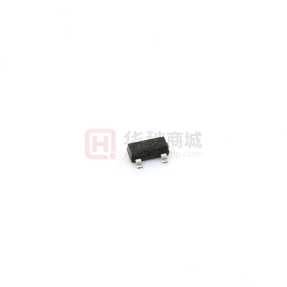
SOT-23
3.Drain
G
S
Maximum ratings ( Ta=25℃ unless otherwise noted)
Parameter
Symbol
Value
Unit
Drain-Source Voltage
VDS
30
V
Gate-Source Voltage
VGS
±12
V
Continuous Drain Current
ID
5.8
A
Drain Current-Pulsed (note 1)
IDM
30
A
Power Dissipation
PD
350
mW
RθJA
357
℃/W
Junction Temperature
TJ
150
℃
Storage Temperature
TSTG
-55~+150
℃
Thermal Resistance from Junction to Ambient (note 2)
GUANGDONG HOTTECH
INDUSTRIAL CO., LTD
Page:P4-P1
�Plastic-Encapsulate Mosfets
AO3400
Electrical Characteristics (TA=25°C, unless otherwise noted)
Parameter
Test Condition
Symbol
Min
Typ
Max
Unit
Off Characteristics
Drain-source breakdown voltage
V(BR) DSS
VGS = 0V, ID =250µA
Zero gate voltage drain current
IDSS
VDS =24V,VGS = 0V
Gate-source leakage current
IGSS
VGS =±12V, VDS = 0V
30
V
1
µA
±100
nA
VGS =10V, ID =5.8A
35
mΩ
VGS =4.5V, ID =5A
40
mΩ
VGS =2.5V,ID=4A
52
mΩ
On characteristics
Drain-source on-resistance
RDS(on)
(note 3)
Forward tranconductance
gFS
Gate threshold voltage
Dynamic Characteristics
VGS(th)
VDS =VGS, ID =250µA
8
S
0.7
1.4
V
1050
pF
(note 4,5)
Input capacitance
Ciss
Output capacitance
Coss
Reverse transfer capacitance
Crss
Gate resistance
Rg
Switching Characteristics
VDS =5V, ID =5A
VDS =15V,VGS =0V,f =1MHz
VDS =0V,VGS =0V,f =1MHz
99
pF
77
pF
3.6
Ω
5
ns
(note 4,5)
Turn-on delay time
Turn-on rise time
Turn-off delay time
Turn-off fall time
td(on)
tr
VGS=10V,VDS=15V,
7
ns
td(off)
RL=2.7Ω,RGEN=3Ω
40
ns
6
ns
1
V
tf
Drain-source diode characteristics and maximum ratings
Diode forward voltage (note 3)
VSD
IS=1A,VGS=0V
Note :
1.
Repetitive Rating : Pulse width limited by maximum junction temperature.
2.
Surface Mounted on FR4 Board, t < 5 sec.
3.
Pulse Test : Pulse Width≤300µs, Duty Cycle ≤ 2%.
4.
Guaranteed by design, not subject to production testing.
GUANGDONG HOTTECH
INDUSTRIAL CO., LTD
Page:P4-P2
�Plastic-Encapsulate Mosfets
AO3400
Typical
Characteristics
GUANGDONG HOTTECH
INDUSTRIAL CO., LTD
Page:P4-P3
�Plastic-Encapsulate Mosfets
AO3400
Typical Characteristics
600
5
VDS=15V
ID=4A
500
Capacitance (pF)
VGS (Volts)
4
3
2
1
Ciss
400
300
200
Coss
100
0
0
0
1
2
3
4
5
0
Qg (nC)
Figure 7: Gate-Charge Characteristics
15
1.0
1ms
1s
10ms
10s
DC
10
5
0.1s
0.1
1
10
100
VDS (Volts)
Figure 9: Maximum Forward Biased Safe
Operating Area (Note E)
Zθ JA Normalized Transient
Thermal Resistance
Power (W)
10µs
100µs
10
30
TJ(Max)=150°C
TA=25°C
RDS(ON)
limited
0.1
20
20
TJ(Max)=150°C
TA=25°C
10.0
10
VDS (Volts)
Figure 8: Capacitance Characteristics
100.0
ID (Amps)
Crss
D=Ton/T
TJ,PK=TA+PDM.ZθJA.RθJA
RθJA=90°C/W
0
0.001
0.01
0.1
1
10
100
1000
Pulse Width (s)
Figure 10: Single Pulse Power Rating Junction-toAmbient (Note E)
In descending order
D=0.5, 0.3, 0.1, 0.05, 0.02, 0.01, single pulse
1
PD
0.1
Ton
T
Single Pulse
0.01
0.00001
0.0001
0.001
0.01
0.1
1
10
Pulse Width (s)
Figure 11: Normalized Maximum Transient Thermal Impedance
GUANGDONG HOTTECH
INDUSTRIAL CO., LTD
100
1000
Page:P4-P4
�
很抱歉,暂时无法提供与“AO3400”相匹配的价格&库存,您可以联系我们找货
免费人工找货- 国内价格
- 20+0.13331
- 200+0.12471
- 500+0.11611
- 1000+0.10750
- 3000+0.10320
- 6000+0.09718


 工商网监
湘ICP备2023018690号
工商网监
湘ICP备2023018690号
