Plastic-Encapsulate Mosfets
AO3404
FEATURES
N-Channel MOSFET
The AO3404 uses advanced trench technology to provide
excellent RDS(ON)
and low gate charge. This device may
be used as a load switch or in PWM applications.
D
1.Gate
2.Source
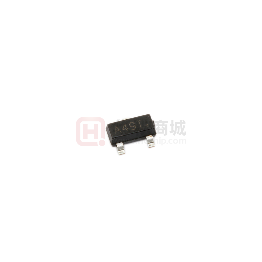
SOT-23
3.Drain
G
S
Absolute Maximum Ratings (TA=25oC, unless otherwise noted)
Parameter
Symbol
Value
Unit
Drain-source voltage
VDS
30
V
Gate-source voltage
VGS
±20
V
Continuous drain current (t ≤10s)
ID
5.8
A
Pulsed drain current *
IDM
30
A
Thermal resistance from junction to ambient
RθJA
357
℃/W
Junction temperature
TJ
150
℃
Storage temperature
Tstg
-55~ 150
℃
Repetitive rating : Pulse width limited by maximum junction temperature.
GUANGDONG HOTTECH
INDUSTRIAL CO., LTD
Page:P4-P1
�Plastic-Encapsulate Mosfets
AO3404
Electrical Characteristics (TA=25°C, unless otherwise noted)
Parameter
Symbol
Test Condition
Min
Typ
Max
Units
STATIC PARAMETERS
V (BR) DSS
VGS = 0V, ID =250µA
Zero gate voltage drain current
IDSS
VDS =30V,VGS = 0V
Gate-body leakage current
IGSS
VGS =±20V, VDS = 0V
Gate threshold voltage
VGS(th)
VDS =VGS, ID =250µA
Drain-source on-resistance (note 1)
RDS(on)
Drain-source breakdown voltage
30
V
1
µA
±100
nA
3
V
VGS =10V, ID =5.8A
30
mΩ
VGS =4.5V, ID =4.8A
42
mΩ
Forward tranconductance (note 1)
gFS
VDS =5V, ID =5.8A
Diode forward voltage
VSD
IS=1A
1
5
S
1
V
820
pF
DYNAMIC PARAMETERS (note 2)
Input capacitance
Ciss
Output capacitance
Coss
Reverse transfer capacitance
Crss
Gate resistance
Rg
VDS =15V,VGS =0V,f =1MHz
118
pF
85
pF
VDS =0V,VGS =0V,f =1MHz
1.5
Ω
6.5
ns
SWITCHING PARAMETERS(note 2)
Turn-on delay time
td(on)
tr
VGS=10V,VDS=15V,
3.1
ns
td(off)
RL=2.6Ω,RGEN=3Ω
15.1
ns
2.7
ns
Turn-on rise time
Turn-off delay time
Turn-off fall time
tf
Note :
1.
Pulse Test : Pulse width≤300µs, duty cycle≤0.5%.
2.
These parameters have no way to verify.
GUANGDONG HOTTECH
INDUSTRIAL CO., LTD
Page:P4-P2
�Plastic-Encapsulate Mosfets
AO3404
Typical
Characteristics
15
30
10V
VDS=5V
7V
25
4.5V
10
20
ID(A)
ID (A)
4V
15
3.5V
5
10
5
VGS=3V
0
0
0
1
2
3
4
VDS (Volts)
Fig 1: On-Region Characteristics (Note E)
1
5
1.5
2
2.5
3
3.5
4
4.5
VGS(Volts)
Figure 2: Transfer Characteristics (Note E)
2
Normalized On-Resistance
40
35
RDS(ON) (mΩ )
25°C
125°C
VGS=4.5V
30
25
VGS=10V
1.8
VGS=10V
ID=5A
1.6
17
5
2
VGS=4.5V10
1.4
1.2
ID=4A
1
0.8
20
0
3
6
9
12
0
15
ID (A)
Figure 3: On-Resistance vs. Drain Current and
Gate Voltage (Note E)
25
50
75
100
125
150
175
0
Temperature (°C)
Figure 4: On-Resistance vs. Junction Temperature
18
(Note E)
100
1.0E+02
ID=5A
1.0E+01
40
1.0E+00
60
IS (A)
RDS(ON) (mΩ )
80
125°C
1.0E-01
1.0E-02
125°C
25°C
1.0E-03
40
1.0E-04
25°C
1.0E-05
20
2
4
6
8
10
VGS (Volts)
Figure 5: On-Resistance vs. Gate-Source Voltage
(Note E)
GUANGDONG HOTTECH
0.0
0.2
0.4
0.6
0.8
1.0
1.2
VSD (Volts)
Figure 6: Body-Diode Characteristics (Note E)
INDUSTRIAL CO., LTD
Page:P4-P3
�Plastic-Encapsulate Mosfets
AO3404
Typical
Characteristics
400
10
VDS=15V
ID=5A
350
300
Capacitance (pF)
VGS (Volts)
8
6
4
Ciss
250
200
150
Coss
100
2
50
0
Crss
0
0
1
2
3
4
5
Qg (nC)
Figure 7: Gate-Charge Characteristics
6
0
100.0
5
10
15
20
25
VDS (Volts)
Figure 8: Capacitance Characteristics
30
10000
TA=25°C
1000
10µs
RDS(ON)
limited
Power (W)
ID (Amps)
10.0
100µs
1.0
1ms
10ms
TJ(Max)=150°C
TA=25°C
0.1
10
10s
DC
0.0
0.01
0.1
1
VDS (Volts)
10
100
1
100
0.00001
0.1
10
1000
Pulse Width (s)
Figure 11: Single Pulse Power Rating Junction-toAmbient (Note F)
Figure 10: Maximum Forward Biased Safe
Operating Area (Note F)
0.001
Zθ JA Normalized Transient
Thermal Resistance
10
D=Ton/T
TJ,PK=TA+PDM.ZθJA.RθJA
1
In descending order
D=0.5, 0.3, 0.1, 0.05, 0.02, 0.01, single pulse
RθJA=125°C/W
0.1
PD
0.01
Single Pulse
Ton
0.001
0.00001
0.0001
0.001
0.01
0.1
1
T
10
100
1000
Pulse Width (s)
Figure 12: Normalized Maximum Transient Thermal Impedance (Note F)
GUANGDONG HOTTECH
INDUSTRIAL CO., LTD
Page:P4-P4
�
很抱歉,暂时无法提供与“AO3404”相匹配的价格&库存,您可以联系我们找货
免费人工找货- 国内价格
- 5+0.21371
- 20+0.19486
- 100+0.17600
- 500+0.15714
- 1000+0.14834
- 2000+0.14206


 工商网监
湘ICP备2023018690号
工商网监
湘ICP备2023018690号
