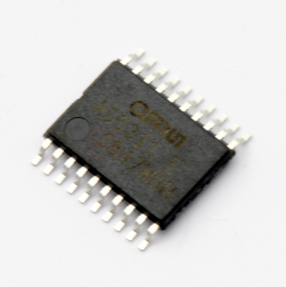
AS5311
Data Sheet
AS5311
Preliminary Data Sheet
High Resolution Magnetic Linear Encoder
1 General Description
The AS5311 is a contactless high resolution magnetic
linear encoder for accurate linear motion and off-axis
rotary sensing with a resolution down to 0
MHz
Clock frequency to read out serial data
www.austriamicrosystems.com
1
Revision 1.04
9 - 24
�AS5311
Data Sheet
6.6.2
Pulse Width Modulation Output
Operating conditions: Tamb = -40 to +125°C, VDD5V = 3.0~3.6V (3V operation) VD D5V = 4.5~5.5V (5V operation) unless
otherwise noted.
Parameter
PWM frequency
Symbol
f PWM
Min
Typ
Max
232
244
256
Unit
Hz
Note
Signal period = 4098µs ±5% at Tamb =
25°C
= 4098µs ±10% at Tamb = -40 to +125°C
220
244
268
Minimum pulse width
PW MIN
0.9
1
1.1
µs
Position 0d =0µm
Maximum pulse width
PW MAX
3892
4097
4301
µs
Position 4095d = 1999.5µm
7 Detailed Description
The different types of outputs relative to the magnet position are outlined in Figure 5 below.
The absolute serial output counts from 0….4095 within one pole pair and repeats with each subsequent pole
pair.
Likewise, the PWM output starts with a pulse width of 1µs, increases the pulse width with every step of 0.488µm
and reaches a maximum pulse width of 4097µs at the end of each pole pair.
An index pulse is generated once for every pole pair.
256 incremental pulses are generated at each output A and B for every pole pair. The outputs A and B are
phase shifted by 90 electrical degrees, which results in 1024 edges per pole pair. As the incremental outputs are
also repeated with every pole pair, a constant train of pulses is generated as the magnet moves over the chip.
Figure 5. AS5311 Outputs Relative to Magnet Position
www.austriamicrosystems.com
Revision 1.04
10 - 24
�AS5311
Data Sheet
7.1 Incremental Outputs
Figure 6 shows the two-channel quadrature output of the AS5311. Output A leads output B when the magnet is
moving from right to left and output B leads output A when the magnet is moving from left to right
(see Figure 14).
Figure 6. Incremental Outputs
M echanical
Z ero P osition
Increm en tal outputs
M ovem ent Direction
Change
M echanical
Zero Position
A
B
Index= 0
1 LSB
In d e x
Movem ent righ t to left
CS n
t
7.1.1
H y st =
2 LSB
Mo vem en t le ft to righ t
In cre m e n tal o u tp u ts va lid
Incremental Power-up Lock Option
After power-up, the incremental outputs can optionally be locked or unlocked, depending on the status of the
CSn pin:
CSn = low at power-up:
CSn has an internal pull-up resistor and must be externally pulled low (Rext ≤ 5kΩ). If Csn is low at
power-up, the incremental outputs A, B and Index will be high until the internal offset compensation is
finished.
This unique state may be used as an indicator for the external controller to shorten the waiting time at
power-up. Instead of waiting for the specified maximum power up-time (see 6.5), the controller can start
requesting data from the AS5311 as soon as the state (A=B=Index = high) is cleared.
CSn = high or open at power-up:
In this mode, the incremental outputs (A, B, Index) will remain at logic high state, until CSn goes low or
a low pulse is applied at CSn. This mode allows intentional disabling of the incremental outputs until for
example the system microcontroller is ready to receive data.
www.austriamicrosystems.com
Revision 1.04
11 - 24
�AS5311
Data Sheet
7.2 Incremental Output Hysteresis
Figure 7. Hysteresis Illustration
Incremental
Output
Indication
X +4
Hysteresis:
2 steps
X +3
X +2
X +1
X
X
Magnet Position
X +1 X +2 X +3 X +4 X +5
Movement left -> right
Movement right -> left
To avoid flickering incremental outputs at a stationary magnet position, a hysteresis is introduced.
In case of a movement direction change, the incremental outputs have a hysteresis of 2 LSB. For constant
movement directions, every magnet position change is indicated at the incremental outputs (see Figure 6). If for
example the magnet moves from position „x+3“ to „x+4“, the incremental output would also indicate this position
accordingly.
A change of the magnet’s movement direction back to position „x+3“ means, that the incremental output still
remains unchanged for the duration of 2 LSB, until position „x+2“ is reached. Following this movement, the
incremental outputs will again be updated with every change of the magnet position.
7.3 Synchronous Serial Interface (SSI)
The Serial interface allows data transmission of the 12-bit absolute linear position information (within one pole
pair = 2.0mm). Data bits D11:D0 represent the position information with a resolution of 488nm (2000µm / 4096)
per step.
CLK must be high at the falling edge of CSn.
Figure 8. Synchronous Serial Interface with Absolute Angular Position Data
tCLK FE
CSn
TCLK/2
tCLK FE
tCSn
1
CLK
DO
8
D11
tDO active
D10
D9
D8
D7
D6
D5
D4
18
D3
D2
D1
D0
OCF
COF
LIN
Mag
INC
tDO valid
Angular Position Data
Status Bits
Mag
DEC
1
Even
PAR
D11
tDO Tristate
If CLK is low at the falling edge of CSn, the first 12 bits represent the magnitude information, which is
proportional to the magnetic field strength. This information can be used to detect the presence and proper
distance of the magnetic strip by comparing it to a known good value (depends on the magnet material and
distance).
The automatic gain control (AGC) maintains a constant MAGnitude value of 3F hex (=”green” range). If the MAG
value is 3F hex, the AGC is out of the regulating range (“yellow” or “red” range). See Table 5 for more details.
www.austriamicrosystems.com
Revision 1.04
12 - 24
�AS5311
Data Sheet
A value of zero or close to zero indicates a missing magnet.
Figure 9. Synchronous Serial Interface with Magnetic Field Strength Data
tCLK FE
CSn
TCLK/2
tCSn
1
CLK
DO
8
M11
M10
M9
M8
M7
M6
M5
M4
18
M3
M2
M1
M0
OCF
COF
LIN
Mag
INC
Mag
DEC
1
Even
PAR
D11
tDO valid
tDO active
tDO Tristate
Magnetic field strength data
Status Bits
If CSn changes to logic low, Data Out (DO) will change from high impedance (tri-state) to logic high and the
read-out will be initiated.
�
After a minimum time t CLK FE, data is latched into the output shift register with the first falling edge of CLK.
�
Each subsequent rising CLK edge shifts out one bit of data.
�
The serial word contains 18 bits, if CLK is high at the falling edge of CSn (Figure 8), the first 12 bits are the
absolute distance information D[11:0], the subsequent 6 bits contain system information, about the validity
of data such as OCF, COF, LIN, Parity and Magnetic Field status (increase/decrease).
�
If CLK is low at the falling edge of CSn (Figure 9), the first 12 bits contain the magnitude information
(range = 00…7F hex) and the subsequent bits contain the status bits (see above)
�
A subsequent measurement is initiated by a “high” pulse at CSn with a minimum duration of t CSn.
7.3.1
Data Contents
D11:D0 absolute linear position data (MSB is clocked out first)
M11:M0 magnitude / magnetic field strength information (MSB is clocked out first)
OCF ( Offset Compensation Finished), logic high indicates the finished Offset Compensation Algorithm
COF (Cordic Over flow), logic high indicates an out of range error in the CORDIC part. When this bit is set,
the data at D11:D0 (likewise M11:M0) is invalid.
This alarm may be resolved by bringing the magnet within the X-Y-Z tolerance limits.
LIN (Linearity Alarm), logic high indicates that the input field generates a critical output linearity.
When this bit is set, the data at D11:D0 may still be used, but can contain invalid data. This warning can be
resolved by increasing the magnetic field strength.
Even Parity bit for transmission error detection of bits 1…17 (D11…D0, OCF, COF, LIN, MagINC, MagDEC)
Data D11:D0 is valid, when the status bits have the following configurations:
Table 4. Status Bit Outputs
OCF
1
COF
0
LIN
0
Mag
INC
Mag
DEC
0
0
0
1
1
0
1*)
1*)
Parity
even checksum of bits 1:17
*) MagInc=MagDec=1 is only recommended in YELLOW mode (see Table 5)
www.austriamicrosystems.com
Revision 1.04
13 - 24
�AS5311
Data Sheet
7.4 Absolute Output Jitter and Hysteresis
Note that there is no hysteresis or additional filtering at the absolute output. This allows a determination of the
magnet’s absolute position within one pole pair down to submicron range.
Due to the intentionally omitted hysteresis and due to noise (e.g. from weak magnetic fields), the absolute output
may jitter when the magnet is stationary over the chip.
In order to get a stable 12-bit absolute reading, two common methods may be implemented to reduce the jitter.
7.4.1
Adding a Digital Hysteresis
The hysteresis feature of the incremental outputs is described in 7.2. An equivalent function can be implemented
in the software of the external microcontroller. The hysteresis should be larger than the peak-to-peak noise
(=jitter) of the absolute output in order to mask it and create a stable output reading.
Remark: the 2-bit hysteresis on the incremental output (=3.9µm) is equivalent to a hysteresis of 8LSB on the
absolute output.
7.4.2
Implementing Digital Filtering
Another useful alternative or additional method to reduce jitter is digital filtering. This can be accomplished
simply by averaging, for example a moving average calculation in the external microcontroller. Averaging 4
readings results in 6dB (=50%) noise and jitter reduction. An average of 16 readings reduces the jitter by a
factor of 4.
Averaging causes additional latency of the processed data. Therefore it may be useful to adjust the depth of
averaging depending on speed of travel. For example using a larger depth when the magnet is stationary and
reducing the depth when the magnet is in motion.
7.5 Z-axis Range Indication (“Red/Yellow/Green” Indicator)
The AS5311 provides several options of detecting the magnet distance by indicating the strength of the
magnetic field. Signal indicators MagINCn and MagDECn are available both as hardware pins (pins 1 and 2) and
as status bits in the serial data stream (see Figure 8). Additionally the LIN status bit indicates the nonrecommended “red” range. The MAGnitude register provides additional information about the strength of the
magnetic field (see Figure 9).
The digital status bits MagINC, MagDec, LIN and the hardware pins MagINCn, MagDECn have the following
function:
Table 5. Magnetic Field Strength Red-Yellow-Green Indicators
Status Bits
MAG
Hardware Pins
Mag
INC
Mag
DEC
LIN
M11..
M0
Mag
INCn
Mag
DECn
0
0
0
3F hex
Off
Off
No distance change
Magnetic input field OK ( GREEN range, ~10…40mT peak
amplitude)
0
1
0
3F hex
Off
Off
Distance increase; this state is a dynamic state and only
active while the magnet is moving away from the chip.
Magnitude register may change but regulates back to 3F hex.
1
0
0
3F hex
Off
Off
Distance decrease; this state is a dynamic state and only
active while the magnet is moving towards the chip.
Magnitude register may change but regulates back to 3F hex.
1
1
0
20 hex5F hex
On
Off
YELLOW range: magnetic field is ~3.4….54.5mT.
The AS5311 may still be operated in this range, but with
slightly reduced accuracy.
1
5F hex
1
1
All other combinations
www.austriamicrosystems.com
On
On
n/a
n/a
Description
RED range: magnetic field is 5F).
It is still possible to operate the AS5311 in the red range, but
not recommended.
Not available
Revision 1.04
14 - 24
�AS5311
Data Sheet
8 Pulse Width Modulation (PWM) Output
The AS5311 provides a pulse width modulated output (PWM), whose duty cycle is proportional to the relative
linear position of the magnet within one pole pair (2.0mm). This cycle repeats after every subsequent pole pair:
Position =
t on ⋅ 4098
(t on + toff ) − 1
for digital position = 0 – 4094
Exception:
A linear position of 1999.5µm = digital position 4095
will generate a pulse width of t on = 4097µs and a pause toff = 1µs
The PWM frequency is internally trimmed to an accuracy of ±5% ( ±10% over full temperature range). This
tolerance can be cancelled by measuring the complete duty cycle as shown above.
Figure 10. PWM Output Signal
Position
PW MIN
0µm
(Pos 0)
1µs
4098µs
PW MA X
1999.5µm
(Pos 4095)
4097µs
1/fPWM
9 3.3V / 5V Operation
The AS5311 operates either at 3.3V ±10% or at 5V ±10%. This is made possible by an internal 3.3V LowDropout (LDO) Voltage regulator. The internal supply voltage is always taken from the output of the LDO,
meaning that the internal blocks are always operating at 3.3V.
For 3.3V operation, the LDO must be bypassed by connecting VDD3V3 with VDD5V (see Figure 11).
For 5V operation, the 5V supply is connected to pin VDD5V, while VDD3V3 (LDO output) must be buffered by a
2.2...10µF capacitor, which is supposed to be placed close to the supply pin.
The VDD3V3 output is intended for internal use only It must not be loaded with an external load.
The output voltage of the digital interface I/O’s corresponds to the voltage at pin VDD5V, as the I/O buffers are
supplied from this pin.
A buffer capacitor of 100nF is recommended in both cases close to pin VDD5V. Note that pin VDD3V3 must
always be buffered by a capacitor. It must not be left floating, as this may cause an instable internal 3.3V supply
voltage which may lead to larger than normal jitter of the measured angle.
www.austriamicrosystems.com
Revision 1.04
15 - 24
�AS5311
Data Sheet
Figure 11. Connections for 5V and 3.3V Supply Voltages
5V Operation
3.3V Operation
2.2...10µF
VDD3V3
VDD3V3
100n
100n
VDD5V
LDO
Internal
VDD
VDD5V
LDO
Internal
VDD
PWM
I
N
T
E
R
F
A
C
E
4.5 - 5.5V
Prog
PWM
DO
3.0 - 3.6V
CLK
CSn
A
B
Prog
Index
VSS
I
N
T
E
R
F
A
C
E
DO
CLK
CSn
A
B
Index
VSS
AS5311
AS5311
10 Magnet Specifications
10.1 Magnetization
The AS5311 accepts magnetic multi-pole strip or ring magnets with a pole length of 1.0mm. Recommended
magnet materials include plastic or rubber bonded ferrite or Neodymium magnets.
It is not recommended to use the AS5311 with other pole lengths as this will create additional nonlinearities.
Figure 12. Additional Error from Pole Length Mismatch
AS5311 Systematic Linearity Error Caused by Pole
Length Deviation
70.00
60.00
Error [µm]
Error 50.00
[µm] 40.00
30.00
20.00
10.00
0.00
750 800 850 900 950 1000 1050 1100 1150 1200 1250
Pole Length [µm]
Figure 12 shows the error caused by a mismatch of pole length. Note that this error is an additional error on top
of the chip-internal INL and DNL errors (see 6.5). For example, when using a multi-pole magnet with 1.2mm pole
length instead of 1.0mm, the AS5311 will provide 1024 incremental steps or 4096 absolute positions over
2.4mm, but with an additional linearity error of up to 50µm.
The curvature of ring magnets may cause linearity errors as well due to the fact that the Hall array on the chip is
a straight line while the poles on the multi-pole ring are curved. These errors decrease with increasing ring
diameter. It is therefore recommended to keep the ring diameter measured at the location of the Hall array at
20mm or higher.
www.austriamicrosystems.com
Revision 1.04
16 - 24
�AS5311
Data Sheet
10.2 Position of the Index Pulse
An index pulse is generated when the North and South poles are placed over the Hall array as shown in
Figure 14.
The incremental output count increases when the magnet is moving to the left, facing the chip with pin#1 at the
lower left corner (see Figure 14, top drawing). At the same time, the absolute position value increases.
Likewise, the position value decreases when the magnet is moved in the opposite direction.
10.3 Mounting the Magnet
10.3.1 Vertical Distance
As a rule of thumb, the gap between chip and magnet should be ½ of the pole length, that is Z=0.5mm for the
1.0mm pole length of the AS5311 magnets. However, the gap also depends on the strength of the magnet.
Typical gaps for AS5311 magnets range from 0.3 to 0.6mm (see 6.4).
The AS5311 automatically adjusts for fluctuating magnet strength by using an automatic gain control (AGC). The
vertical distance should be set such that the AS5311 is in the “green” range. See 7.5 for more details.
10.3.2 Alignment of Multi-pole Magnet and IC
When aligning the magnet strip or ring to the AS5311, the centerline of the magnet strip should be placed
exactly over the Hall array. A lateral displacement in Y-direction (across the width of the magnet) is acceptable
as long as it is within the active area of the magnet. See Figure 14 for the position of the Hall array relative to
Pin #1.
Note: the active area in width is the area in which the magnetic field strength across the width of the magnet is
constant with reference to the centerline of the magnet (see Figure 13 ).
10.3.3 Lateral stroke of Multi-pole Strip Magnets
The lateral movement range (stroke) is limited by the area at which all Hall sensors of the IC are covered by the
magnet in either direction. The Hall array on the AS5311 has a length of 2.0mm, hence the total stroke is
maximum lateral Stroke = Length of active area – length of Hall array
Note: active area in length is defined as the area containing poles with the specified 1.0mm pole length. Shorter
poles at either edge of the magnet must be excluded from the active area (see Figure 13).
Bpk Bpk
Figure 13. Active Area of Strip Magnet
Active Area
Active area (length)
Active area
(width)
B
N
S
2mm
www.austriamicrosystems.com
N
S
N
S
N
S
N
S
recommended
scanning path
strip length
Revision 1.04
17 - 24
�AS5311
Data Sheet
Figure 14. Alignment of Magnet Strip with AS5311 Sensor IC
position value
increases
leftmost magnet position
Die C/L
S
N
S
N
S
N
S
N
S
3.0475±0.235
N
AS5311
Package
Outline
1.00
position value
decreases
rightmost magnet position
S
2.576±0.235
3.200±0.235
Die C/L
N
S
N
S
N
S
N
S
N
1.00
3.0475±0.235
vertical airgap
magnet
strip
carrier
see text
1.00 ± 0.1
www.austriamicrosystems.com
Revision 1.04
Note: all dimensions are in mm
18 - 24
�AS5311
Data Sheet
11 Measurement Data Example
Figure 15 shows typical test results of the accuracy obtained by a commercially available multi-pole magnetic
strip.
The graph shows the accuracy over a stroke of 8mm at two different vertical gaps, 0.2mm and 0.4mm. As
displayed, the accuracy is virtually identical (about +/- 10µm) for both airgaps due to the automatic gain control
of the AS5311 which compensates for airgap changes.
The accuracy depends greatly on the length and strength of each pole and hence from the precision of the tool
used for magnetization as well as the homogeneity of the magnet material. As the error curve in the example
below does not show a repetitive pattern for each pole pair (each 2.0mm), this is most likely an indication that
the pole lengths of this particular sample do not exactly match. While the first pole pair (0...2mm) shows the
greatest nonlinearities, the second pole (2…4mm) is very precise, etc…
Error [µm]
Figure 15. Sample Test Results of INL at Different Airgaps
25
20
15
10
5
0
-5
-10
-15
-20
-25
INL MS10-10
z= 200µ
z= 400µ
0
1000
2000
3000
4000
5000
6000
7000
8000
X [µm]
Note: The magnet sample used in Figure 15 is a 10-pole plastic bonded ferrite magnet as shown in Figure 13.
The corresponding magnet datasheet (MS10-10) is available for download from the austriamicrosystems
website, magnet samples can be ordered from the austriamicrosystems online web shop.
www.austriamicrosystems.com
Revision 1.04
19 - 24
�AS5311
Data Sheet
12 AS5311 Off-axis Rotary Applications
The AS5311 can also be used as an off-axis rotary encoder, as shown in Figure 3. In such applications, the
multi-pole magnetic strip is replaced by a multi-pole magnetic ring. The ring can have radial or axial
magnetization.
Figure 16. Angular Resolution and Maximum Speed versus Ring Diameter
In off-axis rotary applications, very high
angular resolutions are possible with the
AS5311.
The number of steps per revolution
increases linearly with ring diameter.
Due to the increasing number of pulses per
revolution, the maximum speed decreases
with increasing ring diameter.
AS5311 off-axis rotary resolution & speed
160000
700
resolution
speed rpm
140000
600
500
100000
400
80000
300
60000
max. speed [rpm]
resolution [steps / rev]
120000
Example:
a magnetic ring with 41.7mm diameter has
a resolution of 65536 steps per revolution
(16-bit) and a maximum speed of 305 rpm
200
40000
100
20000
0
0
20
40
60
80
100
ring diameter [mm]
Res
[bit]
Steps /
Rev.
Ring
Diameter
[mm]
Max
Speed
[rpm]
15
32768
20.9
609
16
65536
41.7
305
17
131072
83.4
152
The number of incremental steps per revolution can be calculated as:
incremental _ steps = 1024 * nbr _ polepairs
incremental _ steps =
1024 * d * π
2
Note that the circumference (d*π) must be a multiple of one polepair = 2mm, hence the diameter of the magnet
ring may need to be adjusted accordingly:
d=
nbr _ polepairs * 2mm
π
The maximum rotational speed can be calculated as:
max_ rot _ speed =
max_ lin _ speed * 60 39000
=
d *π
d *π
where
nbr_polepairs
d
= the number of pole pairs at the magnet ring
= diameter of the ring in mm; the diameter is taken at the locus of the Hall elements
underneath the magnet
max_rot_speed = maximum rotational speed in revolutions per minute rpm :
max_lin_speed = maximum linear speed in mm/sec (=650 mm/s for AS5311)
Note:
further examples are shown in the “Magnet Selection Guide”, available for download from the
austriamicrosystems website
http://www.austriamicrosystems.com/eng/Products/Magnetic-Encoders/Linear-Encoders
www.austriamicrosystems.com
Revision 1.04
20 - 24
�AS5311
Data Sheet
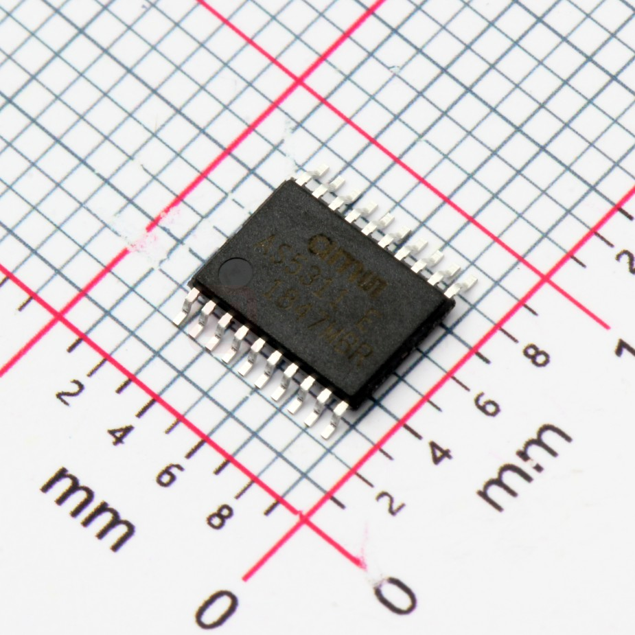
13 Package Drawings and Marking
20 Lead Thin Shrink Small Outline Package – TSSOP20
Figure 17. AS5311 Package Dimensions and Hall Array Location
0.2299±0.100
Die C/L
2.576±0.235
3.200±0.235
0.2341±0.100
Package
Outline
0.7701±0.150
3.0475±0.235
www.austriamicrosystems.com
Revision 1.04
21 - 24
�AS5311
Data Sheet
Dimensions
Marking: AYWWIZZ
mm
inch
Symbol
Min
Typ
Max
Min
Typ
Max
A
-
-
1.10
-
-
0.043
A1
0.05
-
0.15
0.002
-
0.006
A2
0.85
0.90
0.95
0.033
0.035
0.037
b
0.19
-
0.30
0.007
-
0.012
c
0.09
-
0.20
0.004
-
0.008
D
6.40
6.50
6.60
E
6.20
6.40
6.60
0.244
0.252
0.260
E1
4.30
4.40
4.50
0.169
0.173
0.177
e
0.65
.0256
K
0°
-
8°
L
0.50
0.60
0.75
0°
0.019
-
JEDEC Package Outline Standard:
MO – 153
Thermal Resistance R th(j-a) :
89 K/W in still air, soldered on PCB.
IC's marked with a white dot or the letters
"ES" denote Engineering Samples
8°
0.024
A: Pb-Free Identifier
Y: Last Digit of Manufacturing Year
WW: Manufacturing Week
I: Plant Identifier
ZZ: Traceability Code
0.030
14 Ordering Information
Delivery:
Tape and Reel: 1 reel = 1000 devices
1 reel = 4500 devices
Tubes: 1 box = 100 tubes à 74 devices
Order # AS5311ASSU
Order # AS5311ASST
for delivery in tubes
for delivery in tape and reel
15 Recommended PCB Footprint
Recommended Footprint Data
www.austriamicrosystems.com
A
mm
7.00
inch
0.276
B
5.00
0.197
C
0.38
0.015
D
0.65
0.026
E
6.23
0.245
Revision 1.04
22 - 24
�AS5311
Data Sheet
16 Revision History
Revision
Date
Owner
Description
1.01
26-Jun-09
jja, jlu
1.02
09-Apr-10
agt
Delivery information updated
1.03
24-Sep-10
agt
Fig.9 updated
1.04
14-March-11
mub
Table 4. Parity bit change 1…17
Recommended footprint data updated
IC Marking Fig. 17
17 Copyrights
Copyright © 2010, austriamicrosystems AG, Schloss Premstaetten, 8141 Unterpremstaetten, Austria – Europe.
Trademarks Registered ®. All rights reserved. The material herein may not be reproduced, adapted, merged,
translated, stored, or used without the prior written consent of the copyright owner.
All products and companies mentioned are trademarks or registered trademarks of their respective companies.
18 Disclaimer
Devices sold by austriamicrosystems AG are covered by the warranty and patent indemnification provisions
appearing in its Term of Sale. austriamicrosystems AG makes no warranty, express, statutory, implied, or by
description regarding the information set forth herein or regarding the freedom of the described devices from
patent infringement. austriamicrosystems AG reserves the right to change specifications and prices at any time
and without notice. Therefore, prior to designing this product into a system, it is necessary to check with
austriamicrosystems AG for current information. This product is intended for use in normal commercial
applications. Applications requiring extended temperature range, unusual environmental requirements, or high
reliability applications, such as military, medical life-support or lifesustaining equipment are specifically not
recommended without additional processing by austriamicrosystems AG for each application.
The information furnished here by austriamicrosystems AG is believed to be correct and accurate. However,
austriamicrosystems AG shall not be liable to recipient or any third party for any damages, including but not
limited to personal injury, property damage, loss of profits, loss of use, interruption of business or indirect,
special, incidental or consequential damages, of any kind, in connection with or arising out of the furnishing,
performance or use of the technical data herein. No obligation or liability to recipient or any third party shall arise
or flow out of austriamicrosystems AG rendering of technical or other services.
Contact Information
Headquarters
austriamicrosystems AG
A-8141 Schloss Premstaetten, Austria
Tel: +43 (0) 3136 500 0
Fax: +43 (0) 3136 525 01
www.austriamicrosystems.com
Revision 1.04
23 - 24
�AS5311
Data Sheet
For Sales Offices, Distributors and Representatives, please visit:
http://www.austriamicrosystems.com/contact
www.austriamicrosystems.com
Revision 1.04
24 - 24
�


 工商网监
湘ICP备2023018690号
工商网监
湘ICP备2023018690号

