29302
29152/29302/29502/29752
High-Current Low-Dropout Regulators
General Description
Features
The 29150/29300/29500/29750 are high current, high
accuracy, low-dropout voltage regulators. Using
proprietary Super β eta PNP® process with a PNP pass
element, these regulators feature 350mV to 425mV (full
load) typical dropout voltages and very low ground current.
Designed for high current loads, these devices also find
applications in lower current, extremely low dropout-critical
systems, where their tiny dropout voltage and ground
current values are important attributes.
The 29150/29300/29500/29750 are fully protected
against overcurrent faults, reversed input polarity, reversed
lead insertion, overtemperature operation, and positive
and negative transient voltage spikes. Five pin fixed
voltage versions feature logic level ON/OFF control and an
error flag which signals whenever the output falls out of
regulation. Flagged states include low input voltage
(dropout), output current limit, overtemperature shutdown,
and extremely high voltage spikes on the input.
On the 29xx1 and 29xx2, the ENABLE pin may be
tied to VIN if it is not required for ON/OFF control. The
29150/29300/29500 are available in 3-pin and 5-pin
TO-220 and surface mount TO-263 (D2Pak) packages.
The 29750 7.5A regulators are available in 3-pin and
5-pin TO-247 packages. The 1.5A, adjustable output
29152 is available in a 5-pin power D-Pak (TO-252)
package.
For applications with input voltage 6V or below, see
HG37xxx LDOs.
• High current capability
29150/29151/29152/29153.................................1.5A
29300/29301/29302/29303.................................... 3A
29500/29501/29502/29503.................................... 5A
29750/29751/29752............................................7.5A
• Low-dropout voltage
• Low ground current
• Accurate 1% guaranteed tolerance
• Extremely fast transient response
• Reverse-battery and “Load Dump” protection
• Zero-current shutdown mode (5-pin versions)
• Error flag signals output out-of-regulation (5-pin
versions)
• Also characterized for smaller loads with industryleading performance specifications
• Fixed voltage and adjustable versions
Applications
•
•
•
•
•
Battery powered equipment
High-efficiency “Green” computer systems
Automotive electronics
High-efficiency linear lower supplies
High-efficiency lost-regulator for switching supply
_________________________________________________________________________________________________________________________
Typical Application**
Adjustable Output Voltage
Fixed Output Voltage
(*See Minimum Load Current Section)
HTTP://WWW.HGSEMI.NET
1
2014 JUN
�29302
Pin Configuration
3-Pin TO-220 (T)
29150/29300/29500
5-Pin TO-220 Fixed Voltage (T)
29151/29301/29501/29751
5-Pin TO-220 Adjustable Voltage (T)
29152/29302/29502
5-Pin TO-220 Adjustable with Flag (T)
29153/29303/29503
3-Pin TO-247 (WT)
29750
5-Pin TO-247 Fixed Voltage (WT)
29751
5-Pin TO-247 Adjustable Voltage (WT)
29752
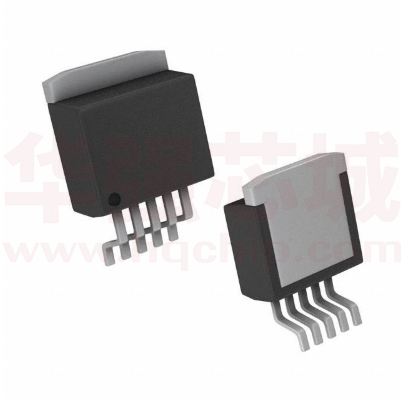
3-Pin TO-263 (D2Pak) (UT)
29150/29300
HTTP://WWW.HGSEMI.NET
2
2014 JUN
�29302
5-Pin TO-263 (D2Pak) Fixed Voltage (U)
29151/29301/29501
5-Pin TO-263 (D2Pak) Adjustable Voltage (U)
29302/29502
5-Pin TO-263 (D2Pak) Adjustable with Flag (U)
29153/29303/29503
5-Pin TO-252 (D-Pak) Adjustable Voltage (D)
29152
Pin Description
Pin Number
TO-220
TO-247
TO-263
Pin Name
1
INPUT: Supplies the current to the output power device
2
GND: TAB is also connected internally to the IC’s ground on D-PAK.
3
OUTPUT: The regulator output voltage
Pin Description
Pin Number
Fixed
TO-220
TO-247
TO-263
Pin Number
Adjustable
TO-220
TO-247
TO-252
TO-263
Pin Number
Adj. with Flag
TO-220
TO-247
TO-263
1
1
—
ENABLE: CMOS compatible control input.
Logic high = enable, logic low = shutdown.
2
2
2
INPUT: Supplies the current to the output power device
3, TAB
3, TAB
3, TAB
Pin Name
GND: TAB is also connected internally to the IC’s ground on D-PAK.
4
4
4
OUTPUT: The regulator output voltage
—
5
5
ADJUST: Adjustable regulator feedback input that connects to the resistor
voltage divider that is placed from OUTPUT to GND in order to set the
output voltage.
5
—
1
FLAG: Active low error flag output signal that indicates an output fault
condition
HTTP://WWW.HGSEMI.NET
3
2014 JUN
�29302
Absolute Maximum Ratings(1)
Operating Ratings(2)
Input Supply Voltage (VIN)(1) ........................... –20V to +60V
Enable Input Voltage (VEN)................................ –0.3V to VIN
Lead Temperature (soldering, 5sec.)......................... 260°C
Power Dissipation .....................................Internally Limited
Storage Temperature Range ....................–65°C to +150°C
ESD Rating................................................................ Note 3
Operating Junction Temperature .............. –40°C to +125°C
Maximum Operating Input Voltage ................................26V
Package Thermal Resistance
TO-220 (θJC).........................................................2°C/W
TO-263 (θJC).........................................................2°C/W
TO-247 (θJC) .....................................................1.5°C/W
TO-252 (θJC).........................................................3°C/W
TO-252 (θJA) ......................................................56°C/W
Electrical Characteristics(4,13)
VIN = VOUT + 1V; IOUT = 10mA; TJ = 25°C, bold values indicate –40°C≤ TJ ≤ +125°C, unless noted.
Parameter
Condition
Output Voltage
IOUT = 10mA
Min
Max
Units
–1
1
%
–2
2
%
0.06
0.5
%
0.2
1
%
20
100
ppm/°C
IOUT = 100mA
IOUT = 750mA
IOUT = 1.5A
IOUT = 100mA
IOUT = 1.5A
IOUT = 3A
IOUT = 250mA
IOUT = 2.5A
IOUT = 5A
IOUT = 250mA
IOUT = 4A
IOUT = 7.5A
80
220
350
80
250
370
125
250
370
80
270
425
200
mV
IOUT = 750mA, VIN = VOUT + 1V
IOUT = 1.5A
IOUT = 1.5A, VIN = VOUT + 1V
IOUT = 3A
IOUT = 2.5A, VIN = VOUT + 1V
IOUT = 5A
IOUT = 4A, VIN = VOUT + 1V
IOUT = 7.5A
8
22
10
37
15
70
35
120
20
mA
35
mA
50
mA
75
mA
IGRNDDOGround Pin
Current at Droupout
VIN = 0.5V less than specified VOUT × IOUT = 10mA
29150
29300
29500
29750
0.9
1.7
2.1
3.1
Current Limit
29150
29300
29500
29750
10mA ≤ IOUT ≤ IFL, (VOUT + 1V) ≤ VIN ≤26V
Line Regulation
Load Regulation
IOUT = 10mA, (VOUT + 1V) ≤ VIN ≤26V
VIN = VOUT + 5V, 10mA ≤ IOUT ≤ 1.5A
(5,9)
(9)
∆VO
∆T
Output Voltage
Temperature Coefficient.
Dropout Voltage
∆VOUT = -1% (6)
29150
29300
29500
29750
Ground Current
(5)
29150
29300
29500
29750
Note 8
HTTP://WWW.HGSEMI.NET
VOUT = 0V (7)
VOUT = 0V (7)
VOUT = 0V (7)
VOUT = 0V (7)
Typ
2.1
4.5
7.5
9.5
4
600
175
600
250
600
200
750
mA
mA
mA
mA
3.5
5.0
10.0
15
2014 JUN
A
A
A
A
�29302
Parameter
Condition
Min
en, Output Noise
Voltage
(10Hz to 100kHz)
IL = 100mA
CL = 10µF
400
CL = 33µF
260
Ground Current in
Shutdown
29150/1/2/3 only V
Reference
29xx2/29xx3
EN
= 0.4V
Reference Voltage
1.228
1.215
Reference Voltage
1.203
Adjust Pin
Bias Current
Reference Voltage
Temperature
Coefficient
Typ
Adjust Pin Bias
Current
Temperature
Coefficient
Units
µV
(rms)
2
10
30
µA
µA
1.240
1.252
1.265
V
V
1.277
V
80
120
nA
40
(10)
Max
20
ppm/°C
0.1
nA/°C
Flag Output (Error Comparator) 29xx1/29xx3
Output Leakage
Current
VOH = 26V
0.01
1.00
2.00
µA
Output Low Voltage
Device set for 5V, VIN = 4.5V
IOL = 250µA
220
300
400
mV
Upper Threshold
Voltage
Device set for 5V (11)
Lower Threshold
Voltage
Device set for 5V (11)
75
Hysteresis
Device set for 5V (11)
15
ENABLE Input
40
25
mV
95
140
mV
mV
29xx1/29xx2
Input Logic Voltage
Low (OFF)
High (ON)
Enable Pin
60
V
0.8
2.4
VEN = 26V
Input Current
VEN = 0.8V
Regulator Output
Current in Shutdown
(12)
HTTP://WWW.HGSEMI.NET
100
0.7
10
5
600
750
µA
2
4
µA
500
µA
2014 JUN
�29302
Notes:
1.
Maximum positive supply voltage of 60V must be of limited duration (
很抱歉,暂时无法提供与“LM29302S/TR”相匹配的价格&库存,您可以联系我们找货
免费人工找货- 国内价格
- 1+3.62502
- 30+3.50002
- 100+3.25002
- 500+3.00001
- 1000+2.87501


 工商网监
湘ICP备2023018690号
工商网监
湘ICP备2023018690号
