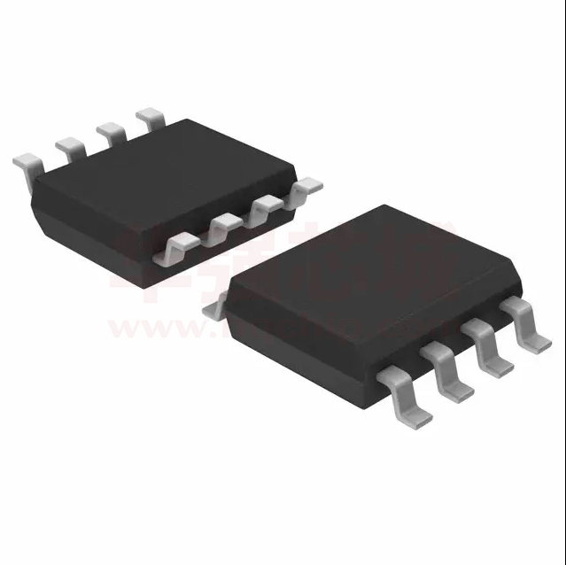
LM358
LM358 Dual Operational Amplifiers
1 Features
2 Applications
•
•
•
•
•
•
•
•
1
•
•
•
•
•
•
•
•
Wide Supply Ranges
– Single Supply: 3 V to 32 V
(26 V for LM2904)
– Dual Supplies: ±1.5 V to ±16 V
(±13 V for LM2904)
Low Supply-Current Drain, Independent of Supply
Voltage: 0.7 mA Typical
Wide Unity Gain Bandwidth: 0.7 MHz
Common-Mode Input Voltage Range Includes
Ground, Allowing Direct Sensing Near Ground
Low Input Bias and Offset Parameters
– Input Offset Voltage: 3 mV Typical
A Versions: 2 mV Typical
– Input Offset Current: 2 nA Typical
– Input Bias Current: 20 nA Typical
A Versions: 15 nA Typical
Differential Input Voltage Range Equal to
Maximum-Rated Supply Voltage: 32 V
(26 V for LM2904)
Open-Loop Differential Voltage Gain:
100 dB Typical
Internal Frequency Compensation
On Products Compliant to MIL-PRF-38535,
All Parameters are Tested Unless Otherwise
Noted. On All Other Products, Production
Processing Does Not Necessarily Include Testing
of All Parameters.
•
•
•
•
Blu-ray Players and Home Theaters
Chemical and Gas Sensors
DVD Recorder and Players
Digital Multimeter: Bench and Systems
Digital Multimeter: Handhelds
Field Transmitter: Temperature Sensors
Motor Control: AC Induction, Brushed DC,
Brushless DC, High-Voltage, Low-Voltage,
Permanent Magnet, and Stepper Motor
Oscilloscopes
TV: LCD and Digital
Temperature Sensors or Controllers Using
Modbus
Weigh Scales
3 Description
These devices consist of two independent, high-gain
frequency-compensated
operational
amplifiers
designed to operate from a single supply or split
supply over a wide range of voltages.
Device Information(1)
PART NUMBER
LMx58, LMx58x,
LM2904, LM2904V
LMx58, LMx58x,
LM2904V
PACKAGE
BODY SIZE (NOM)
VSSOP (8)
3.00 mm × 3.00 mm
SOIC (8)
4.90 mm × 3.90 mm
SO (8)
5.20 mm × 5.30 mm
TSSOP (8)
3.00 mm × 4.40 mm
PDIP (8)
9.81 mm × 6.35 mm
CDIP (8)
9.60 mm × 6.67 mm
LCCC (20)
8.89 mm × 8.89 mm
(1) For all available packages, see the orderable addendum at
the end of the data sheet.
Symbol (Each Amplifier)
IN+
IN−
http://www.hgsemi.com.cn
+
−
1
OUT
2018 AUG
�LM358
5 Pin Configuration and Functions
D, DGK, P, PS, PW and JG Package
8-Pin SOIC, VSSOP, PDIP, SO, TSSOP and CDIP
(Top View)
8
2
7
3
6
4
5
NC
1OUT
NC
V CC+
NC
1
VCC
2OUT
2IN−
2IN+
NC
1IN−
NC
1IN+
NC
4
3 2 1 20 19
18
5
17
6
16
7
15
8
14
9 10 11 12 13
NC
2OUT
NC
2IN−
NC
NC
GND
NC
2IN+
NC
1OUT
1IN−
1IN+
GND
FK Package
20-Pin LCCC
(Top View)
NC - No internal connection
Pin Functions
PIN
LCCC NO.
SOIC, SSOP,
CDIP, PDIP
SO, TSSOP,
CFP NO.
1IN–
5
2
1IN+
7
1OUT
2
2IN–
NAME
I/O
DESCRIPTION
I
Negative input
3
I
Positive input
1
O
Output
15
6
I
Negative input
2IN+
12
5
I
Positive input
2OUT
17
7
O
Output
GND
10
4
—
Ground
—
—
Do not connect
1
3
4
6
8
NC
9
11
13
14
16
18
19
VCC
—
8
—
Power supply
VCC+
20
—
—
Power supply
http://www.hgsemi.com.cn
2
2018 AUG
�LM358
6 Specifications
6.1 Absolute Maximum Ratings
over operating free-air temperature range (unless otherwise noted) (1)
LMx58, LMx58x,
LM2904V
LM2904
UNIT
MIN
MAX
MIN
MAX
VCC
Supply voltage (2)
–0.3
±16 or 32
–0.3
±13 or 26
V
VID
Differential input voltage (3)
–32
32
–26
26
V
Input voltage
–0.3
32
–0.3
26
V
Unlimited
s
either
input
VI
Duration of output short circuit (one amplifier) to ground at
(or below) TA = 25°C,
VCC ≤ 15 V (4)
Unlimited
LM158, LM158A
–55
125
LM258, LM258A
–25
85
LM358, LM358A
0
70
TA
Operating free air temperature
TJ
Operating virtual junction temperature
150
Case temperature for 60
seconds
FK package
260
Lead temperature 1.6 mm (1/16
inch) from case for 60 seconds
JG package
300
LM2904
Tstg
(1)
(2)
(3)
(4)
–40
Storage temperature
–65
°C
125
–40
125
150
°C
°C
150
–65
300
°C
150
°C
Stresses beyond those listed under Absolute Maximum Ratings may cause permanent damage to the device. These are stress ratings
only, and functional operation of the device at these or any other conditions beyond those indicated under Recommended Operating
Conditions is not implied. Exposure to absolute-maximum-rated conditions for extended periods may affect device reliability.
All voltage values (except differential voltages and VCC specified for the measurement of IOS) are with respect to the network GND.
Differential voltages are at IN+, with respect to IN−.
Short circuits from outputs to VCC can cause excessive heating and eventual destruction.
6.2 ESD Ratings
VALUE
V(ESD)
(1)
Electrostatic discharge
Human-body model (HBM), per ANSI/ESDA/JEDEC JS-001 (1)
±500
Charged-device model (CDM), per JEDEC specification JESD22-C101
±1000
UNIT
V
JEDEC document JEP155 states that 500-V HBM allows safe manufacturing with a standard ESD control process.
6.3 Recommended Operating Conditions
over operating free-air temperature range (unless otherwise noted)
LMx58, LMx58x,
LM2904V
VCC
Supply voltage
VCM
Common-mode voltage
TA
Operating free air temperature
http://www.hgsemi.com.cn
LM2904
MAX
MIN
MAX
3
30
3
26
V
0 VCC – 2
V
0
VCC – 2
LM158
–55
125
LM2904
–40
125
LM358
0
70
LM258
–25
85
3
UNIT
MIN
–40
125
°C
2018 AUG
�LM358
6.4 Thermal Information
LMx58, LMx58x, LM2904V, LM2904
THERMAL METRIC (1)
RθJA
LMx58,
LMx58x,
LM2904
V
D (SOIC)
DGK
(VSSOP)
P (PDIP)
PS (SO)
PW
(TSSOP)
FK
(LCCC)
JG
(CDIP)
8 PINS
8 PINS
8 PINS
8 PINS
8 PINS
20 PINS
8 PINS
97
172
85
95
149
—
—
72.2
—
—
—
—
5.61
14.5
Junction-to-ambient
thermal resistance
RθJC(top) Junction-to-case
(top) thermal
resistance
(1)
LMx58,
LMx58x,
LM2904
V
UNIT
°C/W
For more information about traditional and new thermal metrics, see the IC Package Thermal Metrics application report, SPRA953.
6.5 Electrical Characteristics for LMx58
at specified free-air temperature, VCC = 5 V (unless otherwise noted)
PARAMETER
LM158
LM258
TA (2)
TEST CONDITIONS (1)
MIN
VIO
Input offset voltage
αVIO
Average temperature coefficient of
input offset voltage
IIO
Input offset current
αIIO
Average temperature coefficient of
input offset current
IIB
Input bias current
VICR
Common-mode input voltage range
VCC = 5 V to MAX,
VIC = VICR(min),
VO = 1.4 V
25°C
VO = 1.4 V
7
25°C
2
10
25°C
–20
25°C
Large-signal differential
voltage amplification
CMRR
Common-mode rejection ratio
7
9
7
30
2
µV/°C
50
150
10
–150
–20
pA/°C
–250
nA
Full range
25°C
AVD
3
100
Full range
RL ≥ 10 kΩ
VCC = 15 V
VO = 1 V to 11 V,
RL ≥ 2 kΩ
MAX
nA
RL ≥ 2 kΩ
RL ≤ 10 kΩ
TYP (3)
7
Full range
VCC = 5 V to MAX
Low-level output voltage
VOL
5
Full range
VO = 1.4 V
VCC = MAX
3
MIN
mV
Full range
High-level output voltage
UNIT
MAX
Full range
25°C
VOH
TYP
LM358
(3)
–300
–500
0 to
VCC – 1.5
0 to
VCC – 1.5
0 to
VCC – 2
0 to
VCC – 2
VCC – 1.5
VCC – 1.5
26
V
V
RL = 2 kΩ
Full range
26
RL ≥ 10 kΩ
Full range
27
Full range
28
5
27
28
25
100
20
20
mV
50
Full range
25
VCC= 5 V to MAX,
VIC = VICR(min)
25°C
70
80
65
80
dB
kSVR
Supply-voltage rejection ratio
(ΔVDD /ΔVIO)
VCC = 5 V to MAX
25°C
65
100
65
100
dB
VO1/ VO2
Crosstalk attenuation
f = 1 kHz to 20 kHz
25°C
120
dB
VCC = 15 V,
VID = 1 V,
VO = 0
25°C
–20
–30
–20
–30
Full range
–10
25°C
10
Full range
5
VID = –1 V, VO = 200 mV
25°C
12
VCC at 5 V, GND at –5 V,
VO = 0
25°C
±40
±60
±40
±60
VO = 2.5 V, No load
Full range
0.7
1.2
0.7
1.2
VCC = MAX, VO = 0.5 VCC,
No load
Full range
1
2
1
2
IO
Output current
IOS
Short-circuit output current
ICC
Supply current
(two amplifiers)
(1)
(2)
(3)
VCC = 15 V,
VID = –1 V,
VO = 15 V
100
5
25°C
V/mV
15
120
Source
–10
mA
20
10
20
Sink
5
30
12
μA
30
mA
mA
All characteristics are measured under open-loop conditions, with zero common-mode input voltage, unless otherwise specified. MAX
VCC for testing purposes is 26 V for LM2902 and 30 V for the others.
Full range is –55°C to 125°C for LM158, –25°C to 85°C for LM258, and 0°C to 70°C for LM358, and –40°C to 125°C for LM2904.
All typical values are at TA = 25°C
http://www.hgsemi.com.cn
4
2018 AUG
�LM358
6.6 Electrical Characteristics for LM2904
at specified free-air temperature, VCC = 5 V (unless otherwise noted)
TEST CONDITIONS (1)
PARAMETER
VIO
Input offset voltage
MIN
UNIT
TYP (3)
25°C
Non-A-suffix
devices
VCC = 5 V to MAX,
VIC = VICR(min),
VO = 1.4 V
LM2904
TA (2)
MAX
3
7
Full range
10
mV
25°C
1
2
A-suffix devices
Full range
Average temperature coefficient
of input offset voltage
αVIO
4
Full range
7
25°C
2
μV/°C
50
Non-V device
Full range
IIO
Input offset current
VO = 1.4 V
300
nA
25°C
2
50
V-suffix device
Full range
Average temperature coefficient
of input offset current
αIIO
IIB
Input bias current
VICR
Common-mode input
voltage range
VO = 1.4 V
150
Full range
10
25°C
–20
nA
Full range
–500
0 to
VCC – 1.5
25°C
VCC = 5 V to MAX
RL ≥ 10 kΩ
25°C
VCC = MAX,
Non-V device
High-level output voltage
VCC = MAX
V-suffix device
Low-level output voltage
RL ≤ 10 kΩ
AVD
Large-signal differential
voltage amplification
VCC = 15 V,
VO = 1 V to 11 V,
RL ≥ 2 kΩ
CMRR
Common-mode rejection ratio
VCC = 5V to MAX,
VIC = VICR(min)
VOL
VCC – 1.5
RL = 2 kΩ
Full range
22
RL ≥ 10 kΩ
Full range
23
RL = 2 kΩ
Full range
26
Full range
27
28
25°C
25
100
Full range
15
Non-V device
25°C
50
80
V-suffix device
25°C
65
80
65
100
dB
120
dB
–30
RL ≥ 10 kΩ
V
5
20
dB
VCC = 5 V to MAX
25°C
VO1/ VO2
Crosstalk attenuation
f = 1 kHz to 20 kHz
25°C
VCC = 15 V,
VID = 1 V,
VO = 0
25°C
–20
Full range
–10
25°C
10
Full range
5
Source
mA
VCC = 15 V,
VID = –1 V,
VO = 15 V
20
Sink
VID = –1 V, VO = 200 mV
Non-V device
25°C
V-suffix device
25°C
30
12
μA
40
IOS
Short-circuit output current
VCC at 5 V, VO = 0, GND at −5 V
25°C
±40
±60
VO = 2.5 V, No load
Full range
0.7
1.2
ICC
Supply current
(four amplifiers)
VCC = MAX, VO = 0.5 VCC, No load
Full range
1
2
(1)
(2)
(3)
mV
V/mV
Supply-voltage rejection ratio
(ΔVCC /ΔVIO)
Output current
24
Full range
kSVR
IO
V
0 to
VCC – 2
Full range
VOH
pA/°C
–250
mA
mA
All characteristics are measured under open-loop conditions, with zero common-mode input voltage, unless otherwise specified. MAX
VCC for testing purposes is 26 V for LM2902 and 32 V for LM2902V.
Full range is –55°C to 125°C for LM158, –25°C to 85°C for LM258, 0°C to 70°C for LM358, and –40°C to 125°C for LM2904.
All typical values are at TA = 25°C.
6.7 Electrical Characteristics for LM158A and LM258A
at specified free-air temperature, VCC = 5 V (unless otherwise noted)
TEST CONDITIONS (1)
PARAMETER
VIO
(1)
(2)
Input offset voltage
VCC = 5 V to 30 V,
VIC = VICR(min),
VO = 1.4 V
LM158A
TA (1)
MIN
TYP (2)
LM258A
MAX
25°C
2
Full range
4
MIN
TYP (2)
2
UNIT
MAX
3
mV
4
All characteristics are measured under open-loop conditions, with zero common-mode input voltage, unless otherwise specified. MAX
VCC for testing purposes is 26 V for LM2904 and 30 V for others.
All typical values are at TA = 25°C.
http://www.hgsemi.com.cn
5
2018 AUG
�LM358
Electrical Characteristics for LM158A and LM258A (continued)
at specified free-air temperature, VCC = 5 V (unless otherwise noted)
TEST CONDITIONS (1)
PARAMETER
αVIO
Average temperature
coefficient of input
offset voltage
IIO
Input offset current
αIIO
Average temperature
coefficient of input
offset current
IIB
Input bias current
VICR
Common-mode input
voltage range
VO = 1.4 V
LM158A
TA (1)
MAX
Full range
7
25°C
2
VO = 1.4 V
Full range
10
25°C
–15
15 (3)
7
15
10
2
µA/°C
15
30
200
10
–50
–15
200
pA/°C
–80
nA
Full range
–100
VCC = 30 V
RL ≥ 2 kΩ
VCC = 30 V
MAX
30
25°C
–100
0 to
VCC – 1.5
0 to
VCC – 1.5
0 to
VCC – 2
0 to
VCC – 2
VCC – 1.5
VCC – 1.5
Full range
High-level output
voltage
UNIT
TYP (2)
MIN
nA
Full range
25°C
VOH
LM258A
TYP (2)
MIN
RL= 2kΩ
Full range
26
RL≥ 10kΩ
Full range
27
V
26
28
V
27
28
VOL
Low-level output
voltage
RL ≤ 10 kΩ
Full range
Large-signal
differential voltage
amplification
VCC = 15 V, VO = 1 V to 11 V,
RL ≥ 2 kΩ
25°C
50
AVD
Full range
25
CMRR
Common-mode
rejection ratio
25°C
70
80
70
80
dB
kSVR
Supply-voltage
rejection ratio
(ΔVD /ΔVIO)
25°C
65
100
65
100
dB
VO1/ VO2
Crosstalk
attenuation
120
dB
f = 1 kHz to 20 kHz
VCC = 15 V,
VID = 1 V,
VO = 0
IO
Output current
IOS
Short-circuit
output current
ICC
Supply current
(four amplifiers)
(3)
VCC = 15 V,
VID = –1 V,
VO = 15 V
5
20
100
5
50
20
mV
100
V/mV
25°C
25
120
25°C
–20
Full range
–10
25°C
10
–30
–60
–20
−60
–30
Source
–10
mA
20
10
30
12
20
Sink
Full range
5
VID = −1 V, VO = 200 mV
25°C
12
5
VCC at 5 V, GND at –5 V,
VO = 0
25°C
±40
±60
±40
±60
VO = 2.5 V, No load
Full range
0.7
1.2
0.7
1.2
VCC = MAX V, VO = 0.5 V,
No load
Full range
1
2
1
2
μA
30
mA
mA
On products compliant to MIL-PRF-38535, this parameter is not production tested.
6.8 Electrical Characteristics for LM358A
at specified free-air temperature, VCC = 5 V (unless otherwise noted)
PARAMETER
VIO
Input offset voltage
αVIO
Average temperature coefficient
of input offset voltage
IIO
Input offset current
αIIO
Average temperature coefficient
of input offset current
(1)
(2)
(3)
TA (2)
TEST CONDITIONS (1)
VCC = 5 V to 30 V,
VIC = VICR(min),
VO = 1.4 V
25°C
LM358A
MIN
UNIT
TYP (3)
MAX
2
3
mV
Full range
VO = 1.4 V
5
Full range
7
20
25°C
2
30
µA/°C
nA
Full range
Full range
75
10
300
pA/°C
All characteristics are measured under open-loop conditions, with zero common-mode input voltage, unless otherwise specified. MAX
VCC for testing purposes is 26 V for LM2904 and 30 V for others.
All characteristics are measured under open-loop conditions, with zero common-mode input voltage, unless otherwise specified. MAX
VCC for testing purposes is 26 V for LM2904 and 30 V for others.
All typical values are at TA = 25°C.
http://www.hgsemi.com.cn
6
2018 AUG
�LM358
Electrical Characteristics for LM358A (continued)
at specified free-air temperature, VCC = 5 V (unless otherwise noted)
PARAMETER
TEST CONDITIONS (1)
LM358A
TA (2)
MIN
25°C
IIB
Input bias current
VICR
Common-mode input
voltage range
VO = 1.4 V
–15
VCC = 30 V
RL ≥ 2 kΩ
VCC = 30 V
–100
–200
0 to
VCC – 1.5
25°C
V
0 to
VCC – 2
Full range
High-level output voltage
UNIT
MAX
nA
Full range
25°C
VOH
TYP (3)
VCC – 1.5
RL= 2kΩ
Full range
26
RL≥ 10kΩ
Full range
27
28
25°C
25
100
Full range
15
VOL
Low-level output voltage
RL ≤ 10 kΩ
AVD
Large-signal differential
voltage amplification
VCC = 15 V, VO = 1 V to 11 V,
RL ≥ 2 kΩ
Full range
V
5
20
mV
V/mV
CMRR
Common-mode rejection ratio
25°C
65
80
dB
kSVR
Supply-voltage rejection ratio
(ΔVDD /ΔVIO)
25°C
65
100
dB
VO1/ VO2
Crosstalk attenuation
–30
IO
Output current
IOS
Short-circuit output current
ICC
Supply current
(four amplifiers)
f = 1 kHz to 20 kHz
25°C
VCC = 15 V,
VID = 1 V,
VO = 0
25°C
–20
Full range
–10
25°C
10
Full range
5
VCC = 15 V,
VID = –1 V,
VO = 15 V
120
dB
−60
Source
mA
20
Sink
μA
VID = –1 V, VO = 200 mV
25°C
30
VCC at 5 V, GND at –5 V,
VO = 0
25°C
±40
±60
VO = 2.5 V, No load
Full range
0.7
1.2
VCC = MAX V, VO = 0.5 V,
No load
Full range
1
2
mA
mA
6.9 Operating Conditions
VCC = ±15 V, TA = 25°C
TYP
UNIT
SR
Slew rate at unity gain
PARAMETER
RL = 1 MΩ, CL = 30 pF, VI = ±10 V (see Figure 11)
0.3
V/μs
B1
Unity-gain bandwidth
RL = 1 MΩ, CL = 20 pF (see Figure 11)
0.7
MHz
Vn
Equivalent input noise voltage
RS = 100 Ω, VI = 0 V, f = 1 kHz (see Figure 12)
40
nV/√Hz
http://www.hgsemi.com.cn
TEST CONDITIONS
7
2018 AUG
�LM358
6.10 Typical Characteristics
20
0.36
18
0.34
–55C
0C
125C
14
12
10
8
5Vdc
15Vdc
30Vdc
6
4
0.32
Supply Current (mA)
Input Current (nAdc)
16
0.3
0.28
0.26
0.24
0.22
2
0
–55
–35
–15
5
45
25
65
Temperature (°C)
85
105
0.2
125
0
Figure 1. Input Current vs. Temperature
10
15
20
Supply Voltage (Vdc)
25
30
Figure 2. Supply Current vs. Supply Voltage
160
100
CMRR
90
RL=20K
RL=2K
140
80
120
70
100
CMRR (dB)
Avol Voltage Gain (dB)
5
80
60
60
50
40
30
40
20
20
10
0
0
0
5
10
15
20
25
30
V+ Supply Voltage (Vdc)
35
0.1
40
10
100
1000
Frequency (kHz)
C001
Figure 4. Common-mode Rejection Ratio vs. Frequency
Figure 3. Voltage Gain vs. Supply Voltage
0.50
3.5
VOUT
3.0
0.45
2.5
0.40
Voltage (V)
Voltage (V)
1
2.0
1.5
0.35
0.30
1.0
0.25
0.5
VOUT
0.20
0.0
0
4
8
12
16
20
24
Time (�s)
28
32
36
0
40
4
6
Time (�s)
C001
Figure 5. Voltage Follower Large Signal Response (50 pF)
http://www.hgsemi.com.cn
2
8
8
10
C001
Figure 6. Voltage Follower Small Signal Response (50 pF)
2018 AUG
�LM358
Typical Characteristics (continued)
8
Output Voltage (Vdc) relative to Vcc
20
17.5
Output Swing (Vp-p)
15
12.5
10
7.5
5
2.5
0
1
10
100
Frequency (kHz)
7
6
5
4
3
2
1
0.001
1k
Figure 7. Maximum Output Swing vs. Frequency
(VCC = 15 V)
0.1
1
Output Sink Current (mAdc)
10
100
Figure 8. Output Sourcing Characteristics
90
10
5Vdc
15Vdc
30Vdc
80
Output Current (mAdc)
Output Voltage (Vdc)
0.01
1
0.1
70
60
50
40
30
20
10
0.01
0.001
0
0.01
0.1
1
10
Output Sink Current (mAdc)
–55
100
Figure 9. Output Sinking Characteristics
http://www.hgsemi.com.cn
–35
–15
5
45
25
65
Temperature (°C)
85
105
125
Figure 10. Source Current Limiting
9
2018 AUG
�LM358
7 Parameter Measurement Information
900 Ω
VCC+
VCC+
−
VI
100 Ω
VO
+
−
VI = 0 V
RS
VCC−
CL
RL
VO
+
VCC−
Figure 11. Unity-Gain Amplifier
http://www.hgsemi.com.cn
Figure 12. Noise-Test Circuit
10
2018 AUG
�LM358
8 Detailed Description
8.1 Overview
These devices consist of two independent, high-gain frequency-compensated operational amplifiers designed to
operate from a single supply over a wide range of voltages. Operation from split supplies also is possible if the
difference between the two supplies is 3 V to 32 V (3 V to 26 V for the LM2904 device), and VCC is at least 1.5 V
more positive than the input common-mode voltage. The low supply-current drain is independent of the
magnitude of the supply voltage.
Applications include transducer amplifiers, DC amplification blocks, and all the conventional operational amplifier
circuits that now can be implemented more easily in single-supply-voltage systems. For example, these devices
can be operated directly from the standard 5-V supply used in digital systems and easily can provide the required
interface electronics without additional ±5-V supplies.
8.2 Functional Block Diagram
VCC+
≈6-µA
Current
Regulator
≈100-µA
Current
Regulator
≈6-µA
Current
Regulator
OUT
IN−
≈50-µA
Current
Regulator
IN+
GND (or VCC−)
To Other Amplifier
COMPONENT COUNT
Epi-FET
Diodes
Resistors
Transistors
Capacitors
http://www.hgsemi.com.cn
11
1
2
7
51
2
2018 AUG
�LM358
8.3 Feature Description
8.3.1 Unity-Gain Bandwidth
The unity-gain bandwidth is the frequency up to which an amplifier with a unity gain may be operated without
greatly distorting the signal. These devices have a 0.7-MHz unity-gain bandwidth.
8.3.2 Slew Rate
The slew rate is the rate at which an operational amplifier can change its output when there is a change on the
input. These devices have a 0.3-V/μs slew rate.
8.3.3 Input Common Mode Range
The valid common mode range is from device ground to VCC - 1.5 V (VCC - 2 V across temperature). Inputs may
exceed VCC up to the maximum VCC without device damage. At least one input must be in the valid input
common mode range for output to be correct phase. If both inputs exceed valid range then output phase is
undefined. If either input is less than -0.3 V then input current should be limited to 1mA and output phase is
undefined.
8.4 Device Functional Modes
These devices are powered on when the supply is connected. This device can be operated as a single supply
operational amplifier or dual supply amplifier depending on the application.
http://www.hgsemi.com.cn
12
2018 AUG
�LM358
9 Application and Implementation
NOTE
Information in the following applications sections is not part of the TI component
specification, and TI does not warrant its accuracy or completeness. TI’s customers are
responsible for determining suitability of components for their purposes. Customers should
validate and test their design implementation to confirm system functionality.
9.1 Application Information
The LMx58 and LM2904 operational amplifiers are useful in a wide range of signal conditioning applications.
Inputs can be powered before VCC for flexibility in multiple supply circuits.
9.2 Typical Application
A typical application for an operational amplifier in an inverting amplifier. This amplifier takes a positive voltage
on the input, and makes it a negative voltage of the same magnitude. In the same manner, it also makes
negative voltages positive.
RF
Vsup+
RI
VOUT
+
VIN
Vsup-
Figure 13. Application Schematic
9.2.1 Design Requirements
The supply voltage must be chosen such that it is larger than the input voltage range and output range. For
instance, this application will scale a signal of ±0.5 V to ±1.8 V. Setting the supply at ±12 V is sufficient to
accommodate this application.
9.2.2 Detailed Design Procedure
Determine the gain required by the inverting amplifier using Equation 1 and Equation 2:
(1)
(2)
Once the desired gain is determined, choose a value for RI or RF. Choosing a value in the kilohm range is
desirable because the amplifier circuit will use currents in the milliamp range. This ensures the part will not draw
too much current. This example will choose 10 kΩ for RI which means 36 kΩ will be used for RF. This was
determined by Equation 3.
(3)
http://www.hgsemi.com.cn
13
2018 AUG
�LM358
Typical Application (continued)
9.2.3 Application Curve
2
VIN
1.5
VOUT
1
Volts
0.5
0
-0.5
-1
-1.5
-2
0
0.5
1
Time (ms)
1.5
2
Figure 14. Input and Output Voltages of the Inverting Amplifier
10 Power Supply Recommendations
CAUTION
Supply voltages larger than 32 V for a single supply (26 V for the LM2904), or outside
the range of ±16 V for a dual supply (±13 V for the LM2904) can permanently damage
the device (see the Absolute Maximum Ratings).
Place 0.1-μF bypass capacitors close to the power-supply pins to reduce errors coupling in from noisy or high
impedance power supplies. For more detailed information on bypass capacitor placement, refer to the Layout.
11 Layout
11.1 Layout Guidelines
For best operational performance of the device, use good PCB layout practices, including:
• Noise can propagate into analog circuitry through the power pins of the circuit as a whole, as well as the
operational amplifier. Bypass capacitors are used to reduce the coupled noise by providing low impedance
power sources local to the analog circuitry.
– Connect low-ESR, 0.1-μF ceramic bypass capacitors between each supply pin and ground, placed as
close to the device as possible. A single bypass capacitor from V+ to ground is applicable for single
supply applications.
• Separate grounding for analog and digital portions of circuitry is one of the simplest and most-effective
methods of noise suppression. One or more layers on multilayer PCBs are usually devoted to ground planes.
A ground plane helps distribute heat and reduces EMI noise pickup. Make sure to physically separate digital
and analog grounds, paying attention to the flow of the ground current.
• To reduce parasitic coupling, run the input traces as far away from the supply or output traces as possible. If
it is not possible to keep them separate, it is much better to cross the sensitive trace perpendicular as
opposed to in parallel with the noisy trace.
• Place the external components as close to the device as possible. Keeping RF and RG close to the inverting
input minimizes parasitic capacitance, as shown in Layout Examples.
• Keep the length of input traces as short as possible. Always remember that the input traces are the most
sensitive part of the circuit.
• Consider a driven, low-impedance guard ring around the critical traces. A guard ring can significantly reduce
leakage currents from nearby traces that are at different potentials.
http://www.hgsemi.com.cn
14
2018 AUG
�LM358
11.2 Layout Examples
Place components close to
device and to each other to
reduce parasitic errors
Run the input traces as far
away from the supply lines
as possible
RF
NC
NC
GND
IN1í
VCC+
VIN
IN1+
OUT
VCCí
NC
VS+
Use low-ESR, ceramic
bypass capacitor
RG
RIN
GND
Only needed for
dual-supply
operation
GND
VS(or GND for single supply)
VOUT
Ground (GND) plane on another layer
Figure 15. Operational Amplifier Board Layout for Noninverting Configuration
VIN
RIN
+
RG
VOUT
RF
Figure 16. Operational Amplifier Schematic for Noninverting Configuration
http://www.hgsemi.com.cn
15
2018 AUG
�


 工商网监
湘ICP备2023018690号
工商网监
湘ICP备2023018690号

