LMV932
1 MHz Bandwidth Low Power Op Amp
Features
Description
•
•
•
•
•
•
1 MHz Gain Bandwidth Product (typ.)
Rail-to-Rail Input/Output
Supply Voltage: 1.8V to 5.5V
Supply Current: IQ = 100 µA (typ.)
90° Phase Margin (typ.)
Temperature Range:
- Industrial: -40°C to +85°C
- Extended: -40°C to +125°C
• Available in Single, Dual and Quad Packages
LMV932 operational amplifiers (op amps) is specifically
designed for general-purpose applications. This family
has a 1 MHz gain bandwidth product and 90° phase
margin (typ.). It also maintains 45° phase margin (typ.)
with 500 pF capacitive load. This family operates from
a single supply voltage as low as 1.8V, while drawing
100 µA (typ.) quiescent current. Additionally, the
LM932 supports rail-to-rail input and output swing
with a common mode input voltage range of
VDD + 300 mV to V SS - 300 mV. This family of operational amplifiers is designed with Microchip’s
advanced CMOS process.
Applications
The LMV932 family is available in the industrial
and extended temperature ranges. It also has a power
supply range of 1.8V to 5.5V.
•
•
•
•
•
•
Automotive
Portable Equipment
Photodiode Pre-amps
Analog Filters
Notebooks and PDAs
Battery-Powered Systems
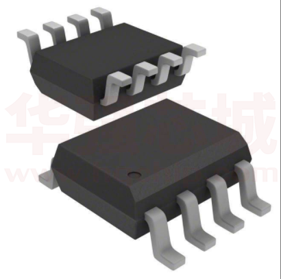
Package Types
LMV932
Typical Application
PDIP, SOIC, MSOP
VDD
VIN
VOUTA 1
VINA– 2
+
VINA+ 3
VOUT
LMV932
-
VSS 4
8 VDD
A
- +
7 VOUTB
B
+ -
6 V
5 V
VSS
R1
R2
VREF
R1
Gain = 1 + -----R2
Non-Inverting Amplifier
1
2016 APR
�LMV932
1.0
ELECTRICAL
CHARACTERISTICS
PIN FUNCTION TABLE
Name
Absolute Maximum Ratings †
VDD - VSS .........................................................................7.0V
All Inputs and Outputs ...................... VSS -0.3V to V DD +0.3V
Difference Input Voltage ....................................... |VDD - VSS|
Output Short Circuit Current ..................................continuous
Current at Input Pins ....................................................±2 mA
Current at Output and Supply Pins ............................±30 mA
Function
V INA+, VINB
Non-inverting Inputs
V INA–, VINB
Inverting Inputs
VDD
Positive Power Supply
VSS
Negative Power Supply
V OUTA, V OUTB
Outputs
Storage Temperature ....................................-65°C to +150°C
Maximum Junction Temperature (TJ) .......................... +150°C
ESD Protection On All Pins (HBM;MM) ............... ≥ 4 kV; 200V
† Notice: Stresses above those listed under “Maximum Ratings” may cause permanent damage to the device. This is a
stress rating only and functional operation of the device at
those or any other conditions above those indicated in the
operational listings of this specification is not implied. Exposure to maximum rating conditions for extended periods may
affect device reliability.
DC ELECTRICAL SPECIFICATIONS
Electrical Characteristics: Unless otherwise indicated, TA = +25°C, VDD = +1.8V to +5.5V, VSS = GND, VCM = VDD /2, RL = 10 kΩ
to VDD /2, and VOUT ~ V DD/2.
Parameters
Sym
Min
Typ
Max
Units
VOS
-7.0
—
+7.0
mV
∆VOS/∆TA
—
±2.0
—
µV/°C
PSRR
—
86
—
dB
Conditions
Input Offset
Input Offset Voltage
Input Offset Drift with Temperature
Power Supply Rejection
VCM = VSS
TA= -40°C to +125°C,
VCM = VSS
VCM = VSS
Input Bias Current and Impedance
Input Bias Current:
IB
—
±1.0
—
pA
Industrial Temperature
IB
—
19
—
pA
TA = +85°C
Extended Temperature
IB
—
1100
—
pA
TA = +125°C
Input Offset Current
IOS
—
±1.0
—
pA
Common Mode Input Impedance
ZCM
—
1013||6
—
Ω||pF
Differential Input Impedance
ZDIFF
—
1013||3
—
Ω||pF
Common Mode Input Range
V CMR
VSS − 0.3
—
VDD + 0.3
V
Common Mode Rejection Ratio
CMRR
60
76
—
dB
VCM = -0.3V to 5.3V, VDD = 5V
AOL
88
112
—
dB
VOUT = 0.3V to VDD - 0.3V,
VCM = VSS
VOL, VOH
VSS + 25
—
V DD − 25
mV
VDD = 5.5V
ISC
—
±6
—
mA
VDD = 1.8V
—
±23
—
mA
VDD = 5.5V
VDD
1.8
—
5.5
V
IQ
50
100
170
µA
Common Mode
Open-Loop Gain
DC Open-Loop Gain (large signal)
Output
Maximum Output Voltage Swing
Output Short-Circuit Current
Power Supply
Supply Voltage
Quiescent Current per Amplifier
http://www.hgsemi.com.cn
2
IO = 0, VDD = 5.5V, VCM = 5V
2016 APR
�LMV932
AC ELECTRICAL SPECIFICATIONS
Electrical Characteristics: Unless otherwise indicated, TA = +25°C, VDD = +1.8 to 5.5V, VSS = GND, VCM = VDD/2,
VOUT ≈ VDD/2, RL = 10 kΩ to VDD/2, and CL = 60 pF.
Parameters
Sym
Min
Typ
Max
Units
GBWP
—
1.0
—
MHz
Conditions
AC Response
Gain Bandwidth Product
Phase Margin
PM
—
90
—
°
Slew Rate
SR
—
0.6
—
V/µs
G = +1
Input Noise Voltage
Eni
—
6.1
—
µVp-p
Input Noise Voltage Density
eni
—
28
—
nV/√Hz
f = 1 kHz
Input Noise Current Density
ini
—
0.6
—
fA/√Hz
f = 1 kHz
Noise
http://www.hgsemi.com.cn
3
f = 0.1 Hz to 10 Hz
2016 APR
�LMV932
2.0
TYPICAL PERFORMANCE CURVES
Note:
The graphs and tables provided following this note are a statistical summary based on a limited number of
samples and are provided for informational purposes only. The performance characteristics listed herein
are not tested or guaranteed. In some graphs or tables, the data presented may be outside the specified
operating range (e.g., outside specified power supply range) and therefore outside the warranted range.
Note: Unless otherwise indicated, TA = +25°C, VDD = +1.8V to +5.5V, VSS = GND, VCM = VDD/2, VOUT ≈ VDD/2,
RL = 10 kΩ to VDD/2, and CL = 60 pF.
100
1225 Samples
VCM = VSS
20%
18%
PSRR, CMRR (dB)
16%
14%
12%
10%
8%
6%
90
PSRR (VCM = VSS)
80
CMRR (VCM = -0.3V to +5.3V)
4%
2%
70
7
6
5
4
-50
-25
0
Input Offset Voltage (mV)
Input Offset Voltage
100
FIGURE 2-4:
Temperature.
VCM = VSS
Open Loop Gain (dB)
PSRR-
70
PSRR+
CMRR
40
-30
80
-60
Phase
60
-90
40
-120
20
30
1.E+04
-20
0.1
1.E+05
10k
1.E-01
100k
1.E+00
1.E+01
1
10
Frequency (Hz)
2%
55%
50%
45%
40%
35%
605 Samples
V DD = 5.5 V
V CM = VDD
TA = +125°C
30%
25%
20%
15%
10%
5%
0%
30
28
26
24
22
20
18
16
14
12
10
8
6
0
0%
4
1.E+07
Input Bias Current (pA)
Input Bias Current at +85°C
1500
4%
2
-210
10M
1400
6%
0
1.E+06
1M
1300
8%
http://www.hgsemi.com.cn
1.E+05
100k
1200
1230 Samples
V DD = 5.5 V
V CM = VDD
TA = +85°C
FIGURE 2-3:
Histogram.
1.E+04
10k
Open-Loop Gain, Phase vs.
300
10%
FIGURE 2-5:
Frequency.
200
12%
PSRR, CMRR vs.
Percentage of Occurrences
Percentage of Occurrences
14%
1.E+03
1k
Frequency (Hz)
100
FIGURE 2-2:
Frequency.
1.E+02
100
1100
1.E+03
1k
900
1.E+02
100
-180
VCM = VSS
1000
1.E+01
10
-150
Gain
0
20
125
100
800
50
100
0
700
60
75
120
600
PSRR, CMRR (dB)
90
80
50
CMRR, PSRR vs. Ambient
500
FIGURE 2-1:
Histogram.
25
Ambient Temperature (°C)
Open Loop Phase (°)
3
2
1
0
-1
-2
-3
-4
-5
-6
-7
0%
400
Percentage of Occurrences
22%
Input Bias Current (pA)
FIGURE 2-6:
Histogram.
4
Input Bias Current at +125°C
2016 APR
�LMV932
Note: Unless otherwise indicated, TA = +25°C, VDD = +1.8V to +5.5V, VSS = GND, VCM = VDD/2, VOUT ≈ VDD/2,
RL = 10 kΩ to VDD/2, and CL = 60 pF.
18%
Percentage of Occurrences
100
2%
Frequency (Hz)
FIGURE 2-7:
vs. Frequency.
FIGURE 2-10:
Histogram.
Input Noise Voltage Density
Input Offset Voltage (µV)
Input Offset Voltage (µV)
12
Input Offset Voltage Drift
200
VDD = 1.8V
-200
-300
-400
TA = -40°C
TA = +25°C
TA = +85°C
TA = +125°C
-500
-600
150
100
50
VDD = 5.5V
0
VDD = 1.8V
-50
-100
-150
V CM = VSS
-200
2.2
2.0
1.8
1.6
1.4
1.2
1.0
0.8
0.6
0.4
0.2
0.0
-0.2
-0.4
-700
0.0
0.5
1.0
1.5
Common Mode Input Voltage (V)
FIGURE 2-11:
Output Voltage.
Output Short Circuit Current
(mA)
VDD = 5.5V
-100
-200
-300
TA = -40°C
TA = +25°C
TA = +85°C
TA = +125°C
-400
-500
-600
-700
-0.5 0.0 0.5 1.0 1.5 2.0 2.5 3.0 3.5 4.0 4.5 5.0 5.5 6.0
2.5
3.0
3.5
4.0
4.5
5.0
5.5
Input Offset Voltage vs.
35
30
+ISC, V DD = 5.5V
25
20
-ISC, V DD = 5.5V
15
-ISC, VDD = 1.8V
10
5
+ISC, VDD = 1.8V
0
-50
Common Mode Input Voltage (V)
-25
0
25
50
75
100
125
Ambient Temperature (°C)
FIGURE 2-9:
Input Offset Voltage vs.
Common Mode Input Voltage at VDD = 5.5V.
http://www.hgsemi.com.cn
2.0
Output Voltage (V)
FIGURE 2-8:
Input Offset Voltage vs.
Common Mode Input Voltage at VDD = 1.8V.
Input Offset Voltage (µV)
8
Input Offset Voltage Drift (µV/°C)
0
-100
0
10
1.E+05
100k
6
1.E+04
10k
4
0%
1.E+03
1k
2
1.E+02
100
4%
0
10
6%
-2
1.E+01
1
8%
-4
1.E+00
10%
-6
1.E-01
0.1
12%
-8
10
f = 0.1 to 10 Hz
14%
-10
Eni = 6.1 µVP-P,
1225 Samples
VCM = VSS
TA = -40°C to +125°C
16%
-12
Input Noise Voltage Density
(nV/Hz)
1,000
FIGURE 2-12:
Output Short-Circuit Current
vs. Ambient Temperature.
5
2016 APR
�LMV932
Note: Unless otherwise indicated, TA = +25°C, VDD = +1.8V to +5.5V, VSS = GND, VCM = VDD/2, VOUT ≈ VDD/2,
RL = 10 kΩ to VDD/2, and CL = 60 pF.
1.0
0.08
0.8
Output Voltage (20 mV/div)
Slew Rate (V/µs)
G = +1 V/V
Falling Edge, VDD = 5.5V
Falling Edge, VDD = 1.8V
0.9
0.7
0.6
0.5
Rising Edge, VDD = 5.5V
Rising Edge, VDD = 1.8V
0.4
0.3
0.2
0.1
0.0
-50
-25
0
25
50
75
100
0.02
0.00
-0. 02
-0. 04
-0. 06
-0. 08
0.E+00
Slew Rate vs. Ambient
1.E-06
2.E-06
3.E-06
4.E-06
1,000
6.E-06
7.E-06
8.E-06
VDD - V OH
VOL - VSS
10
1.E-05
G = +1 V/V
V DD = 5.0V
4.5
100
9.E-06
Small Signal Non-Inverting
5.0
4.0
3.5
3.0
2.5
2.0
1.5
1.0
1
10µ
1.E-05
1.E-04
1.E-03
100µ
1m
0.5
1.E-02
10m
0.0
0.E+00
1.E-05
2.E-05
3.E-05
4.E-05
Output Current Magnitude (A)
5.E-05
6.E-05
7.E-05
8.E-05
9.E-05
1.E-04
Time (10 µs/div)
FIGURE 2-14:
Output Voltage Headroom
vs. Output Current Magnitude.
FIGURE 2-17:
Pulse Response.
Large Signal Non-Inverting
160
10
TA = +125°C
140
VDD = 5.5V
Quiescent Current
per amplifier (mA)
Output Voltage Swing (VP-P)
5.E-06
Time (1 µs/div)
FIGURE 2-16:
Pulse Response.
Output Voltage (V)
Output Voltage Headroom (mV)
0.04
125
Ambient Temperature (°C)
FIGURE 2-13:
Temperature.
0.06
VDD = 1.8V
1
120
TA = 85°C
100
TA = 25°C
80
TA = -40°C
60
40
20
0.1
1.E+03
1k
1.E+04
1.E+05
10k
100k
0.0
1M
Frequency (Hz)
FIGURE 2-15:
Frequency.
Output Voltage Swing vs.
http://www.hgsemi.com.cn
VCM = VDD - 0.5V
0
1.E+06
0.5
1.0
1.5
2.0
2.5
3.0
3.5
4.0
4.5
5.0
5.5
Power Supply Voltage (V)
FIGURE 2-18:
Quiescent Current vs.
Power Supply Voltage.
6
2016 APR
�


 工商网监
湘ICP备2023018690号
工商网监
湘ICP备2023018690号
