HX3415
P-Channel Enhancement Mode MOSFET
Schematic diagram
Description
The HX3415 uses advanced trench technology
to provide excellent RDS(ON), low gate charge and
operation with gate voltages as low as 1.8V. This
device is suitable for use as a load switch or in PWM
applications.
General Features
VDS =-20V,ID =-4A
RDS(ON)(Typ.)=42mΩ @VGS=-2.5V
RDS(ON)(Typ.)=38.3mΩ @VGS=-4.5V
High power and current handing capability
Lead free product is acquired
Surface mount package
ESD Rating: 2500V HBM
Marking and pin assignment
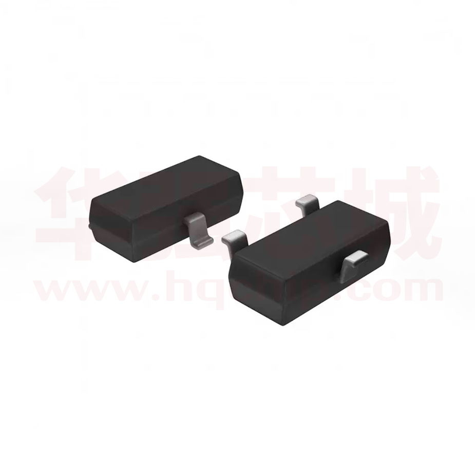
SOT23-3
(TOP VIEW)
Application
D
PWM applications
Load switch
3
Package
SOT-23
1
G
2
S
Ordering Information
Part Number
HX3415
Storage Temperature
Package
Devices Per Reel
-55°C to +150°C
SOT-23
3000
Absolute Maximum Ratings (TA=25℃ unless otherwise noted)
parameter
symbol
limit
unit
Drain-source voltage
VDS
-20
V
Gate-source voltage
VGS
±8
V
Drain current-continuousa@Tj=125℃
-pulse db
ID
-4
A
IDM
-30
A
TA=25℃
Maximum power dissipation
TA=70℃
Operating junction Temperature range
1
PD
Tj
1
1.4
-55—150
W
℃
�HX3415
Electrical Characteristics (TA=25℃ unless otherwise noted)
Parameter
Symbol
Condition
Min
Typ
Max
Unit
OFF Characteristics
Drain-source breakdown voltage
BVDSS
VGS=0V, ID=-250µA
-20
-
-
V
Zero gate voltage drain current
IDSS
VDS=-20V, VGS=0V
-
-
-1
µA
Gate-body leakage
IGSS
VDS=0V, VGS=±8V
-
-
±10
µA
-0.4
-0.59
-0.9
V
VGS=-4.5V, ID=-4A
-
38.3
45
VGS=-2.5V, ID=-4A
-
46.4
60
VGS=-5V, ID=-4A
8
-
-
-
751
-
-
115
-
-
80
-
-
13
-
-
9
-
-
19
-
-
29
-
-
9.3
-
-
1
-
-
2.2
-
-
-0.81
-1.2
ON Characteristics
Gate threshold voltage
VGS(th)
Drain-source on-state resistance
RDS(ON)
Forward transconductance
VDS=VGS, ID=-250µA
gfs
mΩ
S
Dynamic Characteristics
Input capacitance
CISS
Output capacitance
COSS
Reverse transfer capacitance
CRSS
VDS=-10V ,VGS=0V
f=1.0MHz
pF
Switching Characteristics
Turn-on delay time
tD(ON)
Rise time
VDD=-10V
ID=-2.8A
VGEN=-4.5V
RL=10ohm
RGEN=-60ohm
tr
Turn-off delay time
tD(OFF)
Fall time
tf
Total gate charge
Qg
Gate-source charge
Qgs
Gate-drain charge
Qgd
VDS=-10V,ID=-3A
VGS=-4.5V
ns
nC
DRAIN-SOURCE DIODE CHARACTERISTICS
Diode forward voltage
VSD
VGS=0V,Is=-1.25A
Notes:
a. surface mounted on FR4 board,t≤10sec
b. pulse test: pulse width≤300μs,duty≤2%
c. guaranteed by design, not subject to production testing
Thermal Characteristics
Thermal Resistance junction-to ambient
Rth JA
2
100
℃/W
V
�HX3415
Typical Performance Characteristics
3
�HX3415
4
�HX3415
5
�HX3415
Package Information
SOT-23
6
�
HX3415(4A) (SOT-23) 价格&库存
很抱歉,暂时无法提供与“HX3415(4A) (SOT-23)”相匹配的价格&库存,您可以联系我们找货
免费人工找货


 工商网监
湘ICP备2023018690号
工商网监
湘ICP备2023018690号