74AHC1G00; 74AHCT1G00
2-input NAND gate
Rev. 7 — 5 November 2014
Product data sheet
1. General description
74AHC1G00 and 74AHCT1G00 are high-speed Si-gate CMOS devices. They provide a
2-input NAND function.
The AHC device has CMOS input switching levels and supply voltage range 2 V to 5.5 V.
The AHCT device has TTL input switching levels and supply voltage range 4.5 V to 5.5 V.
2. Features and benefits
Symmetrical output impedance
High noise immunity
Low power dissipation
Balanced propagation delays
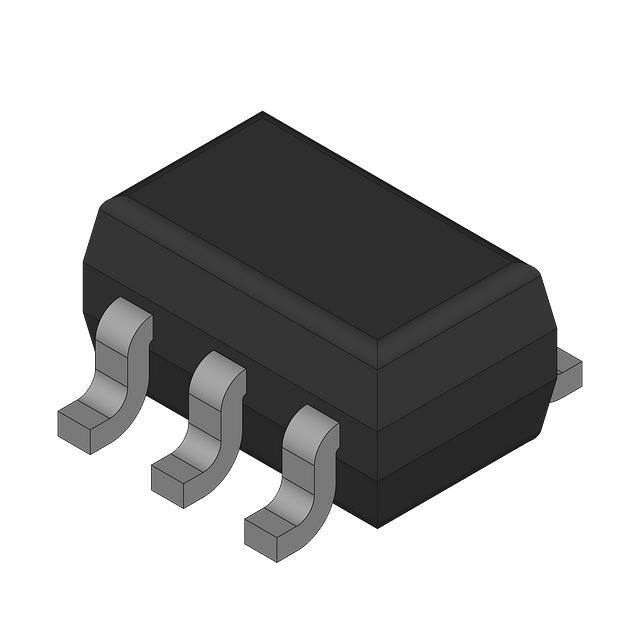
SOT353-1 and SOT753 package options
ESD protection:
HBM JESD22-A114E: exceeds 2000 V
MM JESD22-A115-A: exceeds 200 V
CDM JESD22-C101C: exceeds 1000 V
Specified from 40 C to +125 C
3. Ordering information
Table 1.
Ordering information
Type number
74AHC1G00GW
Package
Temperature range
Name
Description
Version
40 C to +125 C
TSSOP5
plastic thin shrink small outline package;
5 leads; body width 1.25 mm
SOT353-1
40 C to +125 C
SC-74A
plastic surface-mounted package; 5 leads
SOT753
74AHCT1G00GW
74AHC1G00GV
74AHCT1G00GV
�74AHC1G00; 74AHCT1G00
Nexperia
2-input NAND gate
4. Marking
Table 2.
Marking codes
Type number
Marking[1]
74AHC1G00GW
AA
74AHC1G00GV
A00
74AHCT1G00GW
CA
74AHCT1G00GV
C00
[1]
The pin 1 indicator is located on the lower left corner of the device, below the marking code.
5. Functional diagram
�
%
�
$
<
%
�
�
<
�
Logic symbol
$
PQD���
PQD���
Fig 1.
�
Fig 2.
IEC logic symbol
Fig 3.
PQD���
Logic diagram
6. Pinning information
6.1 Pinning
��$+&�*���
��$+&7�*��
%
�
$
�
*1'
�
�
9&&
�
<
���DDI���
Fig 4.
Pin configuration
6.2 Pin description
Table 3.
Pin description
Symbol
Pin
Description
B
1
data input
A
2
data input
GND
3
ground (0 V)
Y
4
data output
VCC
5
supply voltage
74AHC_AHCT1G00
Product data sheet
All information provided in this document is subject to legal disclaimers.
Rev. 7 — 5 November 2014
©
Nexperia B.V. 2017. All rights reserved
2 of 12
�74AHC1G00; 74AHCT1G00
Nexperia
2-input NAND gate
7. Functional description
Table 4.
Function table
H = HIGH voltage level; L = LOW voltage level
Inputs
Output
A
B
Y
L
L
H
L
H
H
H
L
H
H
H
L
8. Limiting values
Table 5.
Limiting values
In accordance with the Absolute Maximum Rating System (IEC 60134).
Symbol
Parameter
Min
Max
Unit
VCC
supply voltage
Conditions
0.5
+7.0
V
VI
input voltage
0.5
+7.0
V
IIK
input clamping current
VI < 0.5 V
20
-
mA
IOK
output clamping current
VO < 0.5 V or VO > VCC + 0.5 V
IO
output current
0.5 V < VO < VCC + 0.5 V
-
20
mA
-
25
mA
ICC
supply current
-
75
mA
IGND
ground current
75
-
mA
Tstg
storage temperature
65
+150
C
Ptot
total power dissipation
-
250
mW
[1]
Tamb = 40 C to +125 C
[2]
[1]
The input and output voltage ratings may be exceeded if the input and output current ratings are observed.
[2]
For both TSSOP5 and SC-74A packages: above 87.5 C the value of Ptot derates linearly with 4.0 mW/K.
9. Recommended operating conditions
Table 6.
Recommended operating conditions
Voltages are referenced to GND (ground = 0 V).
Symbol Parameter
VCC
supply voltage
VI
input voltage
VO
output voltage
Tamb
ambient temperature
t/V
input transition rise
and fall rate
74AHC_AHCT1G00
Product data sheet
Conditions
74AHC1G00
74AHCT1G00
Unit
Min
Typ
Max
Min
Typ
Max
2.0
5.0
5.5
4.5
5.0
5.5
V
0
-
5.5
0
-
5.5
V
0
-
VCC
0
-
VCC
V
40
+25
+125
40
+25
+125
C
VCC = 3.3 V 0.3 V
-
-
100
-
-
-
ns/V
VCC = 5.0 V 0.5 V
-
-
20
-
-
20
ns/V
All information provided in this document is subject to legal disclaimers.
Rev. 7 — 5 November 2014
©
Nexperia B.V. 2017. All rights reserved
3 of 12
�74AHC1G00; 74AHCT1G00
Nexperia
2-input NAND gate
10. Static characteristics
Table 7.
Static characteristics
Voltages are referenced to GND (ground = 0 V).
Symbol Parameter
25 C
Conditions
40 C to +85 C 40 C to +125 C Unit
Min
Typ
Max
Min
Max
Min
Max
VCC = 2.0 V
1.5
-
-
1.5
-
1.5
-
V
VCC = 3.0 V
2.1
-
-
2.1
-
2.1
-
V
VCC = 5.5 V
3.85
-
-
3.85
-
3.85
-
V
VCC = 2.0 V
-
-
0.5
-
0.5
-
0.5
V
VCC = 3.0 V
-
-
0.9
-
0.9
-
0.9
V
VCC = 5.5 V
-
-
1.65
-
1.65
-
1.65
V
HIGH-level
VI = VIH or VIL
output voltage
IO = 50 A; VCC = 2.0 V
1.9
2.0
-
1.9
-
1.9
-
V
IO = 50 A; VCC = 3.0 V
2.9
3.0
-
2.9
-
2.9
-
V
IO = 50 A; VCC = 4.5 V
4.4
4.5
-
4.4
-
4.4
-
V
IO = 4.0 mA; VCC = 3.0 V
2.58
-
-
2.48
-
2.40
-
V
IO = 8.0 mA; VCC = 4.5 V
For type 74AHC1G00
VIH
VIL
VOH
VOL
HIGH-level
input voltage
LOW-level
input voltage
3.94
-
-
3.8
-
3.70
-
V
LOW-level
VI = VIH or VIL
output voltage
IO = 50 A; VCC = 2.0 V
-
0
0.1
-
0.1
-
0.1
V
IO = 50 A; VCC = 3.0 V
-
0
0.1
-
0.1
-
0.1
V
IO = 50 A; VCC = 4.5 V
-
0
0.1
-
0.1
-
0.1
V
IO = 4.0 mA; VCC = 3.0 V
-
-
0.36
-
0.44
-
0.55
V
IO = 8.0 mA; VCC = 4.5 V
-
-
0.36
-
0.44
-
0.55
V
-
-
0.1
-
1.0
-
2.0
A
II
input leakage
current
VI = 5.5 V or GND;
VCC = 0 V to 5.5 V
ICC
supply current VI = VCC or GND; IO = 0 A;
VCC = 5.5 V
-
-
1.0
-
10
-
40
A
CI
input
capacitance
-
1.5
10
-
10
-
10
pF
For type 74AHCT1G00
VIH
HIGH-level
input voltage
VCC = 4.5 V to 5.5 V
2.0
-
-
2.0
-
2.0
-
V
VIL
LOW-level
input voltage
VCC = 4.5 V to 5.5 V
-
-
0.8
-
0.8
-
0.8
V
VOH
HIGH-level
VI = VIH or VIL; VCC = 4.5 V
output voltage
IO = 50 A
4.4
4.5
-
4.4
-
4.4
-
V
3.94
-
-
3.8
-
3.70
-
V
-
0
0.1
-
0.1
-
0.1
V
-
-
0.36
-
0.44
-
0.55
V
-
-
0.1
-
1.0
-
2.0
A
IO = 8.0 mA
VOL
LOW-level
VI = VIH or VIL; VCC = 4.5 V
output voltage
IO = 50 A
IO = 8.0 mA
II
input leakage
current
74AHC_AHCT1G00
Product data sheet
VI = 5.5 V or GND;
VCC = 0 V to 5.5 V
All information provided in this document is subject to legal disclaimers.
Rev. 7 — 5 November 2014
©
Nexperia B.V. 2017. All rights reserved
4 of 12
�74AHC1G00; 74AHCT1G00
Nexperia
2-input NAND gate
Table 7.
Static characteristics …continued
Voltages are referenced to GND (ground = 0 V).
Symbol Parameter
25 C
Conditions
40 C to +85 C 40 C to +125 C Unit
Min
Typ
Max
Min
Max
Min
Max
ICC
supply current VI = VCC or GND; IO = 0 A;
VCC = 5.5 V
-
-
1.0
-
10
-
40
A
ICC
additional
per input pin; VI = 3.4 V;
supply current other inputs at VCC or GND;
IO = 0 A; VCC = 5.5 V
-
-
1.35
-
1.5
-
1.5
mA
CI
input
capacitance
-
1.5
10
-
10
-
10
pF
11. Dynamic characteristics
Table 8.
Dynamic characteristics
GND = 0 V; tr = tf = 3.0 ns. For test circuit see Figure 6.
Symbol Parameter
25 C
Conditions
40 C to +85 C 40 C to +125 C Unit
Min
Typ
Max
Min
Max
Min
Max
-
4.5
7.9
1.0
9.5
1.0
10.5
ns
-
6.5
11.4
1.0
13.0
1.0
14.5
ns
-
3.5
5.5
1.0
6.5
1.0
7.0
ns
-
4.9
7.5
1.0
8.5
1.0
9.5
ns
-
17
-
-
-
-
-
pF
-
3.6
6.2
1.0
7.1
1.0
8.0
ns
-
5.0
7.9
1.0
9.0
1.0
10.0
ns
-
18
-
-
-
-
-
pF
For type 74AHC1G00
tpd
propagation
delay
A and B to Y; see Figure 5
[1]
[2]
VCC = 3.0 V to 3.6 V
CL = 15 pF
CL = 50 pF
[3]
VCC = 4.5 V to 5.5 V
CL = 15 pF
CL = 50 pF
CPD
power
dissipation
capacitance
per buffer;
CL = 50 pF; f = 1 MHz;
VI = GND to VCC
[4]
A and B to Y; see Figure 5
[1]
For type 74AHCT1G00
tpd
propagation
delay
VCC = 4.5 V to 5.5 V
[3]
CL = 15 pF
CL = 50 pF
CPD
power
dissipation
capacitance
[4]
per buffer;
VI = GND to VCC
[1]
tpd is the same as tPLH and tPHL.
[2]
Typical values are measured at VCC = 3.3 V.
[3]
Typical values are measured at VCC = 5.0 V.
[4]
CPD is used to determine the dynamic power dissipation PD (W).
PD = CPD VCC2 fi + (CL VCC2 fo) where:
fi = input frequency in MHz;
fo = output frequency in MHz;
CL = output load capacitance in pF;
VCC = supply voltage in Volts.
74AHC_AHCT1G00
Product data sheet
All information provided in this document is subject to legal disclaimers.
Rev. 7 — 5 November 2014
©
Nexperia B.V. 2017. All rights reserved
5 of 12
�74AHC1G00; 74AHCT1G00
Nexperia
2-input NAND gate
12. Waveforms
90
$��%�LQSXW
W3+/
W3/+
90
很抱歉,暂时无法提供与“74AHC1G00GW,125”相匹配的价格&库存,您可以联系我们找货
免费人工找货- 国内价格 香港价格
- 3000+0.220133000+0.02664
- 12000+0.2191012000+0.02652
- 30000+0.2190930000+0.02652
- 75000+0.2190975000+0.02652
- 120000+0.21908120000+0.02652
- 国内价格 香港价格
- 1+3.370011+0.40787
- 10+2.7312610+0.33056
- 25+2.2895325+0.27710
- 100+1.44994100+0.17549
- 250+1.11918250+0.13545
- 500+0.95379500+0.11544
- 1000+0.648531000+0.07849


 工商网监
湘ICP备2023018690号
工商网监
湘ICP备2023018690号

