Important notice
Dear Customer,
On 7 February 2017 the former NXP Standard Product business became a new company with the
tradename Nexperia. Nexperia is an industry leading supplier of Discrete, Logic and PowerMOS
semiconductors with its focus on the automotive, industrial, computing, consumer and wearable
application markets
In data sheets and application notes which still contain NXP or Philips Semiconductors references, use
the references to Nexperia, as shown below.
Instead of http://www.nxp.com, http://www.philips.com/ or http://www.semiconductors.philips.com/,
use http://www.nexperia.com
Instead of sales.addresses@www.nxp.com or sales.addresses@www.semiconductors.philips.com, use
salesaddresses@nexperia.com (email)
Replace the copyright notice at the bottom of each page or elsewhere in the document, depending on
the version, as shown below:
- © NXP N.V. (year). All rights reserved or © Koninklijke Philips Electronics N.V. (year). All rights
reserved
Should be replaced with:
- © Nexperia B.V. (year). All rights reserved.
If you have any questions related to the data sheet, please contact our nearest sales office via e-mail
or telephone (details via salesaddresses@nexperia.com). Thank you for your cooperation and
understanding,
Kind regards,
Team Nexperia
�PESD5V0U1BA;
PESD5V0U1BB; PESD5V0U1BL
Ultra low capacitance bidirectional ESD protection diodes
Rev. 01 — 25 April 2007
Product data sheet
1. Product profile
1.1 General description
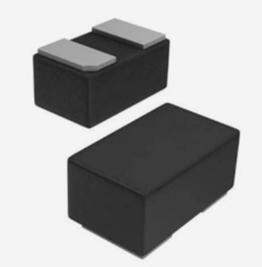
Ultra low capacitance bidirectional ElectroStatic Discharge (ESD) protection diodes in
small Surface-Mounted Device (SMD) plastic packages designed to protect one data line
from the damage caused by ESD.
Table 1.
Product overview
Type number
Package
NXP
JEITA
Package
configuration
PESD5V0U1BA
SOD323
SC-76
very small
PESD5V0U1BB
SOD523
SC-79
flat lead ultra small
PESD5V0U1BL
SOD882
-
leadless ultra small
1.2 Features
n Bidirectional ESD protection of one line n Ultra low leakage current: IRM = 5 nA
n Ultra low diode capacitance: Cd = 2.9 pF n ESD protection of up to 10 kV
n IEC 61000-4-2; level 4 (ESD)
1.3 Applications
n Computers and peripherals
n Audio and video equipment
n Cellular handsets and accessories
n 10/100/1000 Ethernet
n Local Area Network (LAN) equipment
n Communication systems
n Portable electronics
n Subscriber Identity Module (SIM) card
protection
n FireWire
n High-speed data lines
1.4 Quick reference data
Table 2.
Quick reference data
Tamb = 25 °C unless otherwise specified.
Symbol
Parameter
Conditions
Min
Typ
Max
Unit
-
-
5
V
-
2.9
3.5
pF
Per diode
VRWM
reverse standoff voltage
Cd
diode capacitance
f = 1 MHz; VR = 0 V
�PESD5V0U1BA/BB/BL
NXP Semiconductors
Ultra low capacitance bidirectional ESD protection diodes
2. Pinning information
Table 3.
Pinning
Pin
Description
Simplified outline
Symbol
SOD323; SOD523
1
cathode 1
2
cathode 2
[1]
1
2
1
2
sym045
001aab540
SOD882
1
cathode 1
2
cathode 2
[1]
1
2
1
2
sym045
Transparent
top view
[1]
The marking bar indicates the cathode.
3. Ordering information
Table 4.
Ordering information
Type number
Package
Name
Description
Version
PESD5V0U1BA
SC-76
plastic surface-mounted package; 2 leads
SOD323
PESD5V0U1BB
SC-79
plastic surface-mounted package; 2 leads
SOD523
PESD5V0U1BL
-
leadless ultra small plastic package; 2 terminals;
body 1.0 × 0.6 × 0.5 mm
SOD882
4. Marking
Table 5.
Marking codes
Type number
Marking code
PESD5V0U1BA
AA
PESD5V0U1BB
B3
PESD5V0U1BL
AN
PESD5V0U1BA_BB_BL_1
Product data sheet
© NXP B.V. 2007. All rights reserved.
Rev. 01 — 25 April 2007
2 of 12
�PESD5V0U1BA/BB/BL
NXP Semiconductors
Ultra low capacitance bidirectional ESD protection diodes
5. Limiting values
Table 6.
Limiting values
In accordance with the Absolute Maximum Rating System (IEC 60134).
Symbol
Parameter
Conditions
Min
Max
Unit
Per device
Tj
junction temperature
-
150
°C
Tamb
ambient temperature
−65
+150
°C
Tstg
storage temperature
−65
+150
°C
Min
Max
Unit
-
10
kV
-
8
kV
Table 7.
Symbol
ESD maximum ratings
Parameter
Conditions
electrostatic discharge
voltage
IEC 61000-4-2
(contact discharge)
Per diode
VESD
[1][2]
MIL-STD-883 (human
body model)
[1]
Device stressed with ten non-repetitive ESD pulses.
[2]
Measured from pin 1 to pin 2.
Table 8.
ESD standards compliance
Standard
Conditions
Per diode
IEC 61000-4-2; level 4 (ESD)
> 15 kV (air); > 8 kV (contact)
MIL-STD-883; class 3 (human body model)
> 4 kV
001aaa631
IPP
100 %
90 %
10 %
tr = 0.7 ns to 1 ns
t
30 ns
60 ns
Fig 1. ESD pulse waveform according to IEC 61000-4-2
PESD5V0U1BA_BB_BL_1
Product data sheet
© NXP B.V. 2007. All rights reserved.
Rev. 01 — 25 April 2007
3 of 12
�PESD5V0U1BA/BB/BL
NXP Semiconductors
Ultra low capacitance bidirectional ESD protection diodes
6. Characteristics
Table 9.
Characteristics
Tamb = 25 °C unless otherwise specified.
Symbol
Parameter
Conditions
Min
Typ
Max
Unit
Per diode
VRWM
reverse standoff voltage
-
-
5
V
IRM
reverse leakage current
VRWM = 5 V
-
5
100
nA
VBR
breakdown voltage
IR = 5 mA
5.5
7
9.5
V
Cd
diode capacitance
f = 1 MHz
VR = 0 V
-
2.9
3.5
pF
VR = 5 V
-
1.9
-
pF
-
-
100
Ω
differential resistance
rdif
IR = 1 mA
006aab036
3.0
IPP
Cd
(pF)
2.6
−VCL −VBR −VRWM
IR
IRM
−IRM
−IR
VRWM VBR VCL
2.2
−
1.8
0
1
2
3
4
+
−IPP
5
VR (V)
006aaa676
f = 1 MHz; Tamb = 25 °C
Fig 2. Diode capacitance as a function of reverse
voltage; typical values
Fig 3. V-I characteristics for a bidirectional ESD
protection diode
PESD5V0U1BA_BB_BL_1
Product data sheet
© NXP B.V. 2007. All rights reserved.
Rev. 01 — 25 April 2007
4 of 12
�PESD5V0U1BA/BB/BL
NXP Semiconductors
Ultra low capacitance bidirectional ESD protection diodes
ESD TESTER
450 Ω
RZ
RG 223/U
50 Ω coax
4 GHz DIGITAL
OSCILLOSCOPE
10×
ATTENUATOR
50 Ω
CZ
IEC 61000-4-2 network
CZ = 150 pF; RZ = 330 Ω
DUT
(DEVICE
UNDER
TEST)
vertical scale = 10 A/div
horizontal scale = 15 ns/div
vertical scale = 10 V/div
horizontal scale = 100 ns/div
GND
GND
unclamped +8 kV ESD pulse waveform
(IEC 61000-4-2 network)
clamped +8 kV ESD pulse waveform
(IEC 61000-4-2 network) pin 1 to 2
vertical scale = 10 A/div
horizontal scale = 15 ns/div
GND
GND
vertical scale = 10 V/div
horizontal scale = 100 ns/div
unclamped −8 kV ESD pulse waveform
(IEC 61000-4-2 network)
clamped −8 kV ESD pulse waveform
(IEC 61000-4-2 network) pin 1 to 2
006aab037
Fig 4. ESD clamping test setup and waveforms
PESD5V0U1BA_BB_BL_1
Product data sheet
© NXP B.V. 2007. All rights reserved.
Rev. 01 — 25 April 2007
5 of 12
�PESD5V0U1BA/BB/BL
NXP Semiconductors
Ultra low capacitance bidirectional ESD protection diodes
7. Application information
The PESD5V0U1Bx series is designed for the bidirectional protection of one signal line
from the damage caused by ESD pulses. The PESD5V0U1Bx series may be used on
lines where the signal polarities are either positive or negative with respect to ground.
signal line
PESD5V0U1Bx
GND
006aab038
Fig 5. Bidirectional protection of one line
Circuit board layout and protection device placement
Circuit board layout is critical for the suppression of ESD, Electrical Fast Transient (EFT)
and surge transients. The following guidelines are recommended:
1. Place the PESD5V0U1Bx as close to the input terminal or connector as possible.
2. The path length between the PESD5V0U1Bx and the protected line should be
minimized.
3. Keep parallel signal paths to a minimum.
4. Avoid running protected conductors in parallel with unprotected conductors.
5. Minimize all Printed-Circuit Board (PCB) conductive loops including power and
ground loops.
6. Minimize the length of the transient return path to ground.
7. Avoid using shared transient return paths to a common ground point.
8. Ground planes should be used whenever possible. For multilayer PCBs, use ground
vias.
PESD5V0U1BA_BB_BL_1
Product data sheet
© NXP B.V. 2007. All rights reserved.
Rev. 01 — 25 April 2007
6 of 12
�PESD5V0U1BA/BB/BL
NXP Semiconductors
Ultra low capacitance bidirectional ESD protection diodes
8. Package outline
1.35
1.15
0.45
0.15
1
2.7
2.3
0.85
0.75
1.1
0.8
0.65
0.58
1
1.65 1.25
1.55 1.15
1.8
1.6
2
2
0.40
0.25
0.25
0.10
0.34
0.26
Dimensions in mm
03-12-17
Fig 6. Package outline SOD323 (SC-76)
0.17
0.11
Dimensions in mm
02-12-13
Fig 7. Package outline SOD523 (SC-79)
0.50
0.46
0.62
0.55
2
0.30
0.22
0.65
0.30
0.22
1.02
0.95
1
0.55
0.47
cathode marking on top side
Dimensions in mm
03-04-17
Fig 8. Package outline SOD882
PESD5V0U1BA_BB_BL_1
Product data sheet
© NXP B.V. 2007. All rights reserved.
Rev. 01 — 25 April 2007
7 of 12
�PESD5V0U1BA/BB/BL
NXP Semiconductors
Ultra low capacitance bidirectional ESD protection diodes
9. Packing information
Table 10. Packing methods
The indicated -xxx are the last three digits of the 12NC ordering code.[1]
Type number
Package
Description
Packing quantity
3000
8000
10000
PESD5V0U1BA
SOD323
4 mm pitch, 8 mm tape and reel
-115
-
-135
PESD5V0U1BB
SOD523
2 mm pitch, 8 mm tape and reel
-
-315
-
4 mm pitch, 8 mm tape and reel
-115
-
-135
2 mm pitch, 8 mm tape and reel
-
-
-315
PESD5V0U1BL
[1]
SOD882
For further information and the availability of packing methods, see Section 13.
10. Soldering
3.05
2.80
2.10
1.60
solder lands
solder resist
1.65
0.95
0.50
0.60
occupied area
solder paste
0.50
(2×)
msa433
Dimensions in mm
Fig 9. Reflow soldering footprint SOD323 (SC-76)
5.00
4.40
1.40
solder lands
solder resist
occupied area
2.75 1.20
msa415
preferred transport direction during soldering
Dimensions in mm
Fig 10. Wave soldering footprint SOD323 (SC-76)
PESD5V0U1BA_BB_BL_1
Product data sheet
© NXP B.V. 2007. All rights reserved.
Rev. 01 — 25 April 2007
8 of 12
�PESD5V0U1BA/BB/BL
NXP Semiconductors
Ultra low capacitance bidirectional ESD protection diodes
2.15
0.50 0.60
1.20
solder lands
solder paste
0.30
0.40
solder resist
1.80
1.90
occupied area
mgs343
Reflow soldering is the only recommended soldering method.
Dimensions in mm
Fig 11. Reflow soldering footprint SOD523 (SC-79)
1.30
R = 0.05 (8×)
0.30
0.60 0.70 0.80
(2×) (2×) (2×)
0.90
solder lands
solder paste
solder resist
R = 0.05 (8×)
0.30
(2×)
0.40
(2×)
0.50
(2×)
occupied area
mbl872
Reflow soldering is the only recommended soldering method.
Dimensions in mm
Fig 12. Reflow soldering footprint SOD882
PESD5V0U1BA_BB_BL_1
Product data sheet
© NXP B.V. 2007. All rights reserved.
Rev. 01 — 25 April 2007
9 of 12
�PESD5V0U1BA/BB/BL
NXP Semiconductors
Ultra low capacitance bidirectional ESD protection diodes
11. Revision history
Table 11.
Revision history
Document ID
Release date
Data sheet status
Change notice
Supersedes
PESD5V0U1BA_BB_BL_1
20070425
Product data sheet
-
-
PESD5V0U1BA_BB_BL_1
Product data sheet
© NXP B.V. 2007. All rights reserved.
Rev. 01 — 25 April 2007
10 of 12
�PESD5V0U1BA/BB/BL
NXP Semiconductors
Ultra low capacitance bidirectional ESD protection diodes
12. Legal information
12.1 Data sheet status
Document status[1][2]
Product status[3]
Definition
Objective [short] data sheet
Development
This document contains data from the objective specification for product development.
Preliminary [short] data sheet
Qualification
This document contains data from the preliminary specification.
Product [short] data sheet
Production
This document contains the product specification.
[1]
Please consult the most recently issued document before initiating or completing a design.
[2]
The term ‘short data sheet’ is explained in section “Definitions”.
[3]
The product status of device(s) described in this document may have changed since this document was published and may differ in case of multiple devices. The latest product status
information is available on the Internet at URL http://www.nxp.com.
12.2 Definitions
Draft — The document is a draft version only. The content is still under
internal review and subject to formal approval, which may result in
modifications or additions. NXP Semiconductors does not give any
representations or warranties as to the accuracy or completeness of
information included herein and shall have no liability for the consequences of
use of such information.
Short data sheet — A short data sheet is an extract from a full data sheet
with the same product type number(s) and title. A short data sheet is intended
for quick reference only and should not be relied upon to contain detailed and
full information. For detailed and full information see the relevant full data
sheet, which is available on request via the local NXP Semiconductors sales
office. In case of any inconsistency or conflict with the short data sheet, the
full data sheet shall prevail.
12.3 Disclaimers
General — Information in this document is believed to be accurate and
reliable. However, NXP Semiconductors does not give any representations or
warranties, expressed or implied, as to the accuracy or completeness of such
information and shall have no liability for the consequences of use of such
information.
Right to make changes — NXP Semiconductors reserves the right to make
changes to information published in this document, including without
limitation specifications and product descriptions, at any time and without
notice. This document supersedes and replaces all information supplied prior
to the publication hereof.
Suitability for use — NXP Semiconductors products are not designed,
authorized or warranted to be suitable for use in medical, military, aircraft,
space or life support equipment, nor in applications where failure or
malfunction of a NXP Semiconductors product can reasonably be expected to
result in personal injury, death or severe property or environmental damage.
NXP Semiconductors accepts no liability for inclusion and/or use of NXP
Semiconductors products in such equipment or applications and therefore
such inclusion and/or use is at the customer’s own risk.
Applications — Applications that are described herein for any of these
products are for illustrative purposes only. NXP Semiconductors makes no
representation or warranty that such applications will be suitable for the
specified use without further testing or modification.
Limiting values — Stress above one or more limiting values (as defined in
the Absolute Maximum Ratings System of IEC 60134) may cause permanent
damage to the device. Limiting values are stress ratings only and operation of
the device at these or any other conditions above those given in the
Characteristics sections of this document is not implied. Exposure to limiting
values for extended periods may affect device reliability.
Terms and conditions of sale — NXP Semiconductors products are sold
subject to the general terms and conditions of commercial sale, as published
at http://www.nxp.com/profile/terms, including those pertaining to warranty,
intellectual property rights infringement and limitation of liability, unless
explicitly otherwise agreed to in writing by NXP Semiconductors. In case of
any inconsistency or conflict between information in this document and such
terms and conditions, the latter will prevail.
No offer to sell or license — Nothing in this document may be interpreted
or construed as an offer to sell products that is open for acceptance or the
grant, conveyance or implication of any license under any copyrights, patents
or other industrial or intellectual property rights.
12.4 Trademarks
Notice: All referenced brands, product names, service names and trademarks
are the property of their respective owners.
13. Contact information
For additional information, please visit: http://www.nxp.com
For sales office addresses, send an email to: salesaddresses@nxp.com
PESD5V0U1BA_BB_BL_1
Product data sheet
© NXP B.V. 2007. All rights reserved.
Rev. 01 — 25 April 2007
11 of 12
�PESD5V0U1BA/BB/BL
NXP Semiconductors
Ultra low capacitance bidirectional ESD protection diodes
14. Contents
1
1.1
1.2
1.3
1.4
2
3
4
5
6
7
8
9
10
11
12
12.1
12.2
12.3
12.4
13
14
Product profile . . . . . . . . . . . . . . . . . . . . . . . . . . 1
General description. . . . . . . . . . . . . . . . . . . . . . 1
Features . . . . . . . . . . . . . . . . . . . . . . . . . . . . . . 1
Applications . . . . . . . . . . . . . . . . . . . . . . . . . . . 1
Quick reference data. . . . . . . . . . . . . . . . . . . . . 1
Pinning information . . . . . . . . . . . . . . . . . . . . . . 2
Ordering information . . . . . . . . . . . . . . . . . . . . . 2
Marking . . . . . . . . . . . . . . . . . . . . . . . . . . . . . . . . 2
Limiting values. . . . . . . . . . . . . . . . . . . . . . . . . . 3
Characteristics . . . . . . . . . . . . . . . . . . . . . . . . . . 4
Application information. . . . . . . . . . . . . . . . . . . 6
Package outline . . . . . . . . . . . . . . . . . . . . . . . . . 7
Packing information. . . . . . . . . . . . . . . . . . . . . . 8
Soldering . . . . . . . . . . . . . . . . . . . . . . . . . . . . . . 8
Revision history . . . . . . . . . . . . . . . . . . . . . . . . 10
Legal information. . . . . . . . . . . . . . . . . . . . . . . 11
Data sheet status . . . . . . . . . . . . . . . . . . . . . . 11
Definitions . . . . . . . . . . . . . . . . . . . . . . . . . . . . 11
Disclaimers . . . . . . . . . . . . . . . . . . . . . . . . . . . 11
Trademarks . . . . . . . . . . . . . . . . . . . . . . . . . . . 11
Contact information. . . . . . . . . . . . . . . . . . . . . 11
Contents . . . . . . . . . . . . . . . . . . . . . . . . . . . . . . 12
Please be aware that important notices concerning this document and the product(s)
described herein, have been included in section ‘Legal information’.
© NXP B.V. 2007.
All rights reserved.
For more information, please visit: http://www.nxp.com
For sales office addresses, please send an email to: salesaddresses@nxp.com
Date of release: 25 April 2007
Document identifier: PESD5V0U1BA_BB_BL_1
�


 工商网监
湘ICP备2023018690号
工商网监
湘ICP备2023018690号
