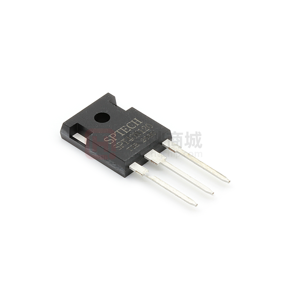
SPT40N120T1B
1200V /40A Trench Field Stop IGBT
FEATURES
High breakdown voltage to 1200V for
VCE
1200
V
IC
40
A
VCE(SAT) IC=40A
1.7
V
improved reliability
Trench-Stop Technology offering :
very tight parameter distribution
high ruggedness, temperature stable
behavior
Short circuit withstand time – 10s
High ruggedness, temperature stable
Low VCE(SAT)
Easy parallel switching capability due
to positive temperature coefficient in
VCE(SAT)
Enhanced avalanche capability
APPLICATION
Frequency Converters
Motor Drive
http://www.superic-tech.com
1
2018.06 / Rev3.3
�SPT40N120T1B
Maximum Ratings
Parameter
Symbol
Value
Unit
Collector-Emitter Breakdown Voltage
VCE
1200
V
DC collector current, limited by Tjmax
TC = 25°C
TC = 100°C
IC
80
40
A
Diode Forward current, limited by Tjmax
TC = 25°C
TC = 100°C
IF
80
40
A
Pulsed Collector Current, limited by Tjmax
ICpuls
160
A
Turn off safe operating area VCE ≤1200V,
Tj ≤ 150°C
-
160
A
Diode Pulsed Current, limited by Tjmax
IFpuls
160
A
Short Circuit Withstand Time, VGE= 15V,
VCE≤ 600V
Tsc
10
μs
Power dissipation , Tj=25℃
Ptot
416
W
Operating junction temperature
Tj
-40...+150
°C
Storage temperature
Ts
-55...+150
°C
Soldering temperature, wave soldering 1.6mm
(0.063in.) from case for 10s
-
260
°C
Thermal Resistance
Parameter
Symbol
Max. Value
Unit
IGBT thermal resistance,
junction - case
Rθ(j-c)
0.3
K/W
Diode thermal resistance,
junction - case
Rθ(j-c)
0.6
K/W
Thermal resistance,
junction - ambient
Rθ(j-a)
40
K/W
http://www.superic-tech.com
2
2018.06 / Rev3.3
�SPT40N120T1B
Electrical Characteristics of the IGBT(Tj= 25℃ unless otherwise specified):
Parameter
Symbol
Conditions
Min.
Typ.
Max.
Unit
Static
Collector-Emitter
breakdown voltage
BVCES
VGE=0V , IC=250μA
1200
1300
-
V
Gate threshold voltage
VGE(th)
VGE=VCE, IC=250μA
5.1
5.8
6.4
V
Collector-Emitter
Saturation voltage
VCE(sat)
VGE=15V, IC=40A
Tj = 25°C
Tj = 150°C
-
1.7
2.1
2.1
-
V
Zero gate voltage
collector current
ICES
VCE = 1200V, VGE = 0V
Tj = 25°C
Tj = 150°C
-
-
10
2500
μA
Gate-emitter
leakage current
IGES
VCE = 0V, VGE = 20V
-
-
100
nA
Transconductance
gfs
VCE=20V, IC=15A
-
15
-
S
Parameter
Symbol
Conditions
Min.
Typ.
Max.
Unit
Dynamic
Input capacitance
Cies
Output capacitance
Coes
Reverse transfer
capacitance
Cres
Gate charge
QG
Short circuit collector
current
IC(SC)
http://www.superic-tech.com
-
4400
-
-
180
-
-
100
-
VCC = 960V, IC = 40A,
VGE = 15V
-
270
-
nC
VGE=15V,tSC≤10us
VCC=600V,
Tj,start=25°C
-
240
-
A
VCE = 25V, VGE = 0V,
f = 1MHz
3
2018.06 / Rev3.3
pF
�SPT40N120T1B
Switching Characteristic, Inductive Load
Parameter
Symbol
Conditions
Min.
Typ.
Max.
Unit
Dynamic , at Tj = 25°C
Turn-on delay time
td(on)
-
55
-
ns
tr
-
20
-
ns
-
2.4
-
mJ
-
230
-
ns
tf
-
160
-
ns
Eoff
-
1.5
-
mJ
Rise time
Turn-on energy
Turn-off delay time
Eon
td(off)
Fall time
Turn-off energy
VCC = 600V, IC = 40A,
VGE = 0/15V,
Rg=12Ω
Electrical Characteristics of the DIODE(Tj= 25℃ unless otherwise specified)
Parameter
Symbol
Conditions
Min.
Typ.
Max.
Unit
Dynamic
Diode Forward Voltage
VFM
Reverse Recovery Time
Trr
Reverse Recovery Current
Irr
Reverse Recovery Charge
Qrr
http://www.superic-tech.com
IF = 40A
IF= 40A,
VR = 600V,
di/dt= 400A/μs,
4
-
3.5
-
V
-
190
-
ns
-
6
-
A
-
530
-
nC
2018.06 / Rev3.3
�SPT40N120T1B
Fig. 1 FBSOA characteristics
Fig. 2 Load Current vs. Frequency
160
140
100
110℃
120
tP = 10μs
100
50μs
10
IC(A)
IC(A)
100μs
500μs
1ms
80
60
DC
1
80℃
40
20
Ta=25℃, Tj ≤150℃ , VGE=15V
0.1
D=0.5, VCE=600V,
VGE=0/15V, Rg=12Ω,Tj ≤150℃
0
1
10
100
1000
1
10
VCE(V)
100
f (KHz)
Fig. 3 Power dissipation as a function of TC
Fig. 4 Short circuit time and current vs.VGE
450
260
400
240
350
220
300
200
250
180
TSC(us)
70
Isc
Tsc
ISC (A)
Ptot(W)
60
200
50
40
160
150
140
100
120
50
100
30
20
Tj ≤150C
Ta=25°
C,Vcc=600V
80
0
25
50
75
100
125
150
9
TC(℃)
http://www.superic-tech.com
10
11
12
13
14
15
10
16
VGE(V)
5
2018.06 / Rev3.3
�SPT40N120T1B
Fig. 5 Output characteristics
Fig. 6 Saturation voltage characteristics
90
90
VGE = 20V
80
80
150℃
17V
70
25℃
70
15V
13V
60
60
11V
9V
50
IC(A)
IC(A)
50
7V
40
40
30
30
20
20
10
10
0
0
VGE = 15V
0
1
2
3
4
5
0
1
2
VCE(V)
3
4
5
6
VCE(V)
Fig. 7 Switching times vs. gate resistor
Fig. 8 Switching times vs. collector current
1000
1000
t, SWITCHING TIMES [ns]
t, SWITCHING TIMES [ns]
td(off)
tf
td(on)
tr
100
100
10
td(off)
tf
td(on)
tr
Common Emitter
VCC = 600V, VGE = 15V, IC=40A
Ta=25℃
Common Emitter
VCC = 600V, VGE = 15V, RG=12Ω
Ta=25℃
1
10
0
5
10
15
20
25
30
35
40
45
10
20
30
40
50
60
70
80
90
IC(A)
Rg (Ω)
http://www.superic-tech.com
0
6
2018.06 / Rev3.3
�SPT40N120T1B
Fig. 9 Switching loss vs. gate resistor
Fig. 10 Switching loss vs. collector current
4.5
12
Eoff
Eon
Eoff
Eon
4
Common Emitter
VCC = 600V, VGE = 15V,
RG=12Ω Ta=25℃
10
3
Switching loss (mJ)
Switching loss (mJ)
3.5
2.5
2
1.5
8
6
4
1
2
Common Emitter
VCC = 600V, VGE = 15V,
IC=40A Ta=25℃
0.5
0
0
0
5
10
15
20
25
30
35
40
45
0
10
20
30
Rg (Ω)
40
50
60
70
80
90
Ic (A)
Fig. 11 Gate charge characteristics
Fig. 12 Capacitance characteristics
10000
15
240V
600V
960V
12
Ciss(pF)
Coss(pF)
1000
Crss(pF)
Capacitance
VGE (V)
9
6
100
3
Common Emitter
VGE = 0V, f = 1MHz
Ta=25℃
Common Emitter
IC= 40A ,Ta=25℃
0
10
0
50
100
150
200
250
300
10
20
VCE(V)
Qg (nC)
http://www.superic-tech.com
0
7
2018.06 / Rev3.3
30
�SPT40N120T1B
http://www.superic-tech.com
8
2018.06 / Rev3.3
�


 工商网监
湘ICP备2023018690号
工商网监
湘ICP备2023018690号

