XZ298N
..
..
.
nectionof an externalsensing resistor. Anadditional
supply input is provided so that the logic works at a
lower voltage.
OPERATING SUPPLY VOLTAGE UP TO 46 V
TOTAL DC CURRENT UP TO 4 A
LOW SATURATION VOLTAGE
OVERTEMPERATURE PROTECTION
LOGICAL ”0” INPUT VOLTAGE UP TO 1.5 V
(HIGH NOISE IMMUNITY)
DESCRIPTION
The XZ298N is an integrated monolithic circuit in a
15-lead Multiwatt and PowerZIP15 packages. It
is ahigh voltage, high current dual full-bridge driver
de-signed to accept standardTTL logic levels and
driveinductive loads such as relays, solenoids,
DC andstepping motors. Two enableinputs are
provided toenableor disable the
deviceindependentlyof the in-put signals. The
emitters of the lower transistors ofeach bridge are
connected together and the corre-sponding
external terminal can be used for the conBLOCK DIAGRAM
1
�XZ298N
ZIP15
2
�XZ298N
PIN FUNCTIONS (refer to the block diagram)
MW.15
Po werSO
Name
1;15
2;19
Sense A; Sense B
Between this pin and ground is connected the sense resistor to
control the current of the load.
Fun ction
2;3
4;5
Out 1; Out 2
Outputs of the Bridge A; the current that flows through the load
connected between these two pins is monitored at pin 1.
4
6
VS
Supply Voltage for the Power Output Stages.
A non-inductive 100nF capacitor must be connected between this
pin and ground.
5;7
7;9
Input 1; Input 2
6;11
8;14
Enable A; Enable B
TTL Compatible Inputs of the Bridge A.
8
1,10,11,20
GND
Ground.
9
12
VSS
Supply Voltage for the Logic Blocks. A100nF capacitor must be
connected between this pin and ground.
10; 12
13;15
Input 3; Input 4
13; 14
16;17
Out 3; Out 4
–
3;18
N.C.
TTL Compatible Enable Input: the L state disables the bridge A
(enable A) and/or the bridge B (enable B).
TTL Compatible Inputs of the Bridge B.
Outputs of the Bridge B. The current that flows through the load
connected between these two pins is monitored at pin 15.
Not Connected
ELECTRICAL CHARACTERISTICS (VS = 42V; VSS = 5V, Tj = 25°C; unless otherwise specified)
Symbol
Parameter
VS
Supply Voltage (pin 4)
VSS
Logic Supply Voltage (pin 9)
Test Co nditions
Operative Condition
Min .
4.5
Ven = H; IL = 0
Typ .
VIH +2.5
Unit
46
V
5
7
V
13
50
22
70
mA
mA
4
mA
24
7
36
12
mA
mA
6
mA
1.5
V
IS
Quiescent Supply Current (pin 4)
ISS
Quiescent Current from VSS (pin 9) Ven = H; IL = 0
V iL
Input Low Voltage
(pins 5, 7, 10, 12)
–0.3
ViH
Input High Voltage
(pins 5, 7, 10, 12)
2.3
VSS
V
IiL
Low Voltage Input Current
(pins 5, 7, 10, 12)
Vi = L
–10
µA
IiH
High Voltage Input Current
(pins 5, 7, 10, 12)
Vi = H ≤ VSS –0.6V
100
µA
Ven = L
Vi = L
Vi = H
Max.
Vi = X
Ven = L
Vi = L
Vi = H
Vi = X
30
Ven = L
Enable Low Voltage (pins 6, 11)
–0.3
1.5
V
Ven = H
Enable High Voltage (pins 6, 11)
2.3
VSS
V
Ien = L
Low Voltage Enable Current
(pins 6, 11)
Ven = L
–10
µA
Ien = H
High Voltage Enable Current
(pins 6, 11)
Ven = H ≤ VSS –0.6V
30
100
µA
0.95
1.35
2
1.7
2.7
V
V
1.2
1.7
1.6
2.3
V
V
VCEsat (H) Source Saturation Voltage
IL = 1A
IL = 2A
VCEsat (L) Sink Saturation Voltage
IL = 1A
IL = 2A
(5)
(5)
0.85
IL = 1A
IL = 2A
(5)
(5)
1.80
3.2
4.9
V
V
–1 (1)
2
V
VCEsat
Total Drop
Vsens
Sensing Voltage (pins 1, 15)
3
�XZ298N
ELECTRICAL CHARACTERISTICS (continued)
Symbol
Parameter
Test Co nditions
Min .
Typ .
Max.
Unit
T1 (Vi)
Source Current Turn-off Delay
0.5 V i to 0.9 I L
(2); (4)
1.5
µs
T2 (Vi)
Source Current Fall Time
0.9 IL to 0.1 IL
(2); (4)
0.2
µs
T3 (Vi)
Source Current Turn-on Delay
0.5 V i to 0.1 I L
(2); (4)
2
µs
T4 (Vi)
Source Current Rise Time
0.1 IL to 0.9 IL
(2); (4)
0.7
µs
T5 (Vi)
Sink Current Turn-off Delay
0.5 V i to 0.9 I L
(3); (4)
0.7
µs
T6 (Vi)
Sink Current Fall Time
0.9 IL to 0.1 IL
(3); (4)
0.25
µs
T7 (Vi)
Sink Current Turn-on Delay
0.5 V i to 0.9 I L
(3); (4)
1.6
µs
T8 (Vi)
Sink Current Rise Time
0.1 IL to 0.9 IL
(3); (4)
0.2
µs
fc (Vi)
Commutation Frequency
IL = 2A
T1 (Ven)
Source Current Turn-off Delay
0.5 V en to 0.9 IL
25
T2 (Ven)
Source Current Fall Time
0.9 IL to 0.1 IL
T3 (Ven)
Source Current Turn-on Delay
0.5 V en to 0.1 IL
T4 (Ven)
Source Current Rise Time
0.1 IL to 0.9 IL
T5 (Ven)
Sink Current Turn-off Delay
0.5 V en to 0.9 IL
(2); (4)
(2); (4)
(2); (4)
(2); (4)
T6 (Ven)
Sink Current Fall Time
0.9 IL to 0.1 IL
T7 (Ven)
Sink Current Turn-on Delay
0.5 V en to 0.9 IL
T8 (Ven)
Sink Current Rise Time
0.1 IL to 0.9 IL
(3); (4)
(3); (4)
(3); (4)
(3); (4)
40
µs
1
µs
0.3
µs
0.4
µs
2.2
µs
0.35
µs
0.25
µs
0.1
µs
1) 1)Sensing voltage can be –1 V for t ≤ 50 µsec; in steady state V sens min ≥ – 0.5 V.
2) See fig. 2.
3) See fig. 4.
4) The load must be a pure resistor.
Figure 1 : Typical Saturation Voltage vs. Output
Current.
Figure 2 : Switching Times Test Circuits.
XZ298N
Note : For INPUT Switching, set EN = H
For ENABLESwitching, set IN = H
4
KHz
3
�XZ298N
Figure 3 : Source Current Delay Times vs. Input or Enable Switching.
Figure 4 : Switching Times Test Circuits.
XZ298N
Note : For INPUT Switching, set EN = H
For ENABLE Switching, set IN = L
5
�XZ298N
Figure 5 : Sink Current Delay Times vs. Input 0 V Enable Switching.
Figure 6 : Bidirectional DC Motor Control.
In pu ts
Ven = H
Ven = L
L = Low
XZ298N
6
Fu nctio n
C=H;D=L
Forward
C =L; D= H
Reverse
C=D
Fast Motor Stop
C=X;D=X
Free Running
Motor Stop
H = High
X = Don’t care
�XZ298N
Figure 7 : For higher currents, outputs can be paralleled. Take care to parallel channel 1 with channel 4
and channel 2 with channel 3.
XZ298N
APPLICATION INFORMATION (Refer to the block diagram)
1.1. POWER OUTPUT STAGE
Each input must be connected to the source of the
driving signals by means of a very short path.
The XZ298N integratestwo poweroutputstages
(A ;B).The power output stage is a bridge
Turn-On and Turn-Off : Before to Turn-ON the Supconfigurationand its outputs can drive an
ply Voltageand beforeto Turnit OFF, the Enableininductive load in com-mon or differenzialmode,
put must be driven to the Low state.
dependingon the state ofthe inputs. The current
3. APPLICATIONS
that flows through the loadcomes out from the
bridge at the sense output : anexternal resistor
Fig 6 shows a bidirectional DC motor control Sche(RSA ; RSB.) allows to detect the in-tensity of this
matic Diagram for which only one bridge is needed.
The external bridge of diodes D1 to D4 is made by
current.
four fast recovery elements (trr ≤ 200 nsec) that
1.2. INPUT STAGE
must be chosen of a VF as low as possible at the
Each bridge is driven by means of four gates the inworst case of the load current.
put of which are In1 ; In2 ; EnA and In3 ; In4 ; EnB.
The sense outputvoltage can be used to control the
The In inputs set the bridge state when The En input
current amplitude by chopping the inputs, or to prois high ; a lowstate of the En inputinhibitsthe bridge.
vide overcurrent protection by switching low the enAll the inputs are TTL compatible.
able input.
2. SUGGESTIONS
The brake function (Fast motor stop) requires that
the Absolute Maximum Rating of 2 Amps must
A non inductive capacitor, usually of 100 nF, must
never be overcome.
be foreseen between both Vs and Vss, to ground,
as near as possible to GND pin. When the large caWhen the repetitive peak current needed from the
pacitor of the power supply is too far from the IC, a
load is higher than 2 Amps, a paralleled configurasecond smaller one must be foreseen near the
tion can be chosen (See Fig.7).
XZ298N.
An external bridge of diodes are required when inThe sense resistor, not of a wire wound type, must
ductive loads are driven and when the inputs of the
be grounded near the negative pole of Vs that must
IC are chopped; Shottkydiodeswould bepreferred.
be near the GND pin of the I.C.
7
�XZ298N
This solution can drive until 3 Amps In DC operation
and until 3.5 Amps of a repetitive peak current.
OnFig 8 it is shownthe driving ofa twophasebipolar
stepper motor ; the needed signals to drive the inputs of the XZ298N are generated, in this
example,from the IC XD297.
Fig 9 shows an example of P.C.B. designed for the
application of Fig 8.
Fig 10 shows a second two phase bipolar stepper
motor control circuit where the current is controlled
by the I.C. L6506.
Figure 8 : Two Phase Bipolar Stepper Motor Circuit.
This circuit drives bipolar stepper motors with winding currents up to 2 A. The diodes are fast 2 A types.
XD297
XZ298N
RS1 = RS2 = 0.5 Ω
D1 to D8 = 2 A Fast diodes
{
VF ≤ 1.2 V @ I = 2 A
trr ≤ 200 ns
8
�XZ298N
mm
DIM.
MIN.
TYP.
inch
MAX.
MIN.
TYP.
A
5
0.197
B
2.65
0.104
C
1.6
D
OUTLINE AND
MECHANICAL DATA
MAX.
0.063
1
0.039
E
0.49
0.55
0.019
F
0.66
0.75
0.026
0.022
G
1.02
1.27
1.52
0.040
0.050
0.060
G1
17.53
17.78
18.03
0.690
0.700
0.710
H1
19.6
0.030
0.772
H2
20.2
0.795
L
21.9
22.2
22.5
0.862
0.874
0.886
L1
21.7
22.1
22.5
0.854
0.870
0.886
L2
17.65
18.1
0.695
L3
17.25
17.5
17.75
0.679
0.689
0.699
L4
10.3
10.7
10.9
0.406
0.421
0.429
L7
2.65
2.9
0.104
0.713
0.114
M
4.25
4.55
4.85
0.167
0.179
0.191
M1
4.63
5.08
5.53
0.182
0.200
0.218
S
1.9
2.6
0.075
S1
1.9
2.6
0.075
0.102
0.102
Dia1
3.65
3.85
0.144
0.152
Multiwatt15 V
9
�
很抱歉,暂时无法提供与“XZ298N”相匹配的价格&库存,您可以联系我们找货
免费人工找货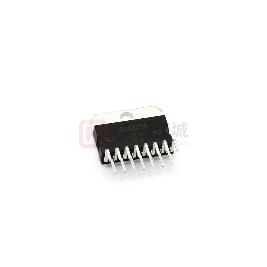


 工商网监
湘ICP备2023018690号
工商网监
湘ICP备2023018690号

