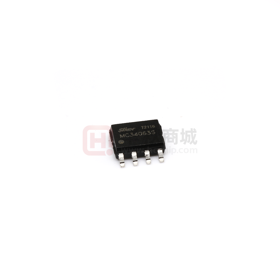
MC34063
DC TO DC CONVERTER CONTROLLER
DESCRIPTION
The MC34063 is a monolithic regulator subsystem,
intended for use as DC to DC converter. This device contains a
temperature compensated band gap reference, a duty-cycle
control oscillator, driver and high current output switch. It can be
used for step down, step-up or inverting switching regulators as
well as for series pass regulators.
MC34063D DIP-8
FEATURES
* Operation from 3.0V to 40V.
* Short circuit current limiting.
* Low standby current.
* Output switch current of 1.5A without external transistors.
* Frequency of operation from 100Hz to 100kHz.
* Step-up, step-down or inverting switch regulators.
PIN CONFIGURATION
PIN DESCRIPTION
PIN NO
1
2
3
4
6
PIN NAME
Switch Collector
Switch Emitter
Timing Capacitor
GND
Comparator Inverting
Input
VCC
7
IPEAK Sense
I
8
Driver Collector
I
5
www.slkormicro.com
I/O
I
O
I
MC34063S SOP-8
DESCRIPTION
Internal Darlington pairs TI collector
Internal Darlington pairs TI emitter
The value of selected capacitor controls the internal oscillator run rate
Inverting input of comparator which can set & initiate the Darlington pairs
output switch
Current sense input to monitor the voltage drop across an external
resistor placed in series with VCC
Internal Darlington pairs TI collector
1
�MC34063
BLOCK DIAGRAM
E
Switch Collector
T2
1
S
Q
R
T1
Switch Emitter
8
Drive Collector
7
IPEAK Sense
6
Vcc
5
Comparator Inverting
Input
D
C
2
A
Is
CT
OSCILLATOR
Timing Capacitor
3
COMP.
GND
4
1.25VREF
B
ABSOLUTE MAXIMUM RATINGS (Ta=25°C )
PARAMETER
Supply Voltage
Comparator Input Voltage Range
Switch Collector Voltage
Switch Emitter Voltage
Switch Collector to Emitter Voltage
Driver Collector Voltage
Switch Current
RATINGS
UNIT
40
V
-0.3 ~ +40
V
40
V
40
V
40
V
40
V
1.5
A
DIP-8
1250
Power Dissipation (Ta=25°C)
PD
mW
SOP-8
625
Junction Temperature
TJ
+150
°C
Operating Temperature
TOPR
0 ~ +70
°C
Storage Temperature
TSTG
-65 ~ +150
°C
Note: Absolute maximum ratings are those values beyond which the device which the device could be permanently
damaged. Absolute maximum ratings are stress ratings only and functional device operation is not implied.
SYMBOL
VCC
VIN(COMP)
VC(SW)
VE(SW)
VCE(SW)
VC(DR)
ISW
THERMAL DATA
PARAMETER
Junction-to-Ambient
www.slkormicro.com
SYMBOL
DIP-8
SOP-8
2
θJA
RATINGS
100
160
UNIT
℃/W
�MC34063
ELECTRICAL CHARACTERISTICS (VCC=5.0V, Ta=0~+70°C, unless otherwise specified.)
PARAMETER
Oscillator
Charging Current
Discharging Current
Oscillator Amplitude
Discharge to Charge Current Ratio
Current limit Sense Voltage
Output Switch
Saturation Voltage 1(Note)
Saturation Voltage 2(Note)
DC Current Gain(Note)
Collector Off State Current(Note)
Comparator
Threshold Voltage
Threshold Voltage Line Regulation
Input Bias Current
Total Device
SYMBOL
ICHG
IDISCHG
VOSC
K
VSENSE
VCE(SAT)1
VCE(SAT)2
GI (DC)
IC(OFF)
VTHD
VTHD
II(BIAS)
TEST CONDITIONS
VCC=5 to 40V, Ta=25°C
VCC=5 to 40V, Ta=25°C
Ta=25°C
V7=VCC, Ta=25°C
ICHG=IDISCHG, Ta=25°C
MIN
TYP MAX UNIT
22
140
31
190
0.5
6.1
300
42
260
7.5
350
mV
0.95
0.45
180
0.01
1.3
0.7
V
V
100
μA
1.21 1.24 1.29
2.0
5.0
50
400
V
mV
nA
5.2
250
ISW=1.0A, VC(DRIVER)=VC(SW)
ISW=1.0A, VC(DRIVER)=50mA
ISW=1.0A, VCE=5.0V, Ta=25°C
VCE=40.0V, Ta=25°C
VCC=3 ~ 40V
VIN=0V
50
VCC=5~40V, CT=0.001
V7=VCC, VC>VTHD, Pin2=GND
Note: Output switch tests are performed under pulsed conditions to minimize power dissipation.
Supply Current
ICC
2.7
4.0
μA
μA
V
mA
STEP-UP CONVERTER(Cont.)
170μH
L
1
8
180
S Q
Q2
R
Q1
7
2
1N5819
IPK
RSC 0.22
VIN12V
OSC
6
+
100
CT
3
CT
VCC
+
- Comp.
1.25V
REF REG
5
1500pF
4
1.0μH
R2
R1
2.2k
47k
330
+
CO
VOUT
28V/175mA
VOUT
+
100
Optional Filter
www.slkormicro.com
3
�MC34063
STEP-DOWN CONVERTER(Cont.)
VOLTAGE INVERTING CONVERTER
www.slkormicro.com
4
�MC34063
DESIGN FORMULA TABLE
CALCULATION
tON
tOFF
STEP-DOWN
STEP-UP
VOLTAGE-INVERTING
VOUT + VF
VIN - VCE(SAT)
(tON+tOFF)MAX
CT
4x10⁻⁵ tON
ISW
2IOUT(MAX)
RS
0.3/ISW
4x10⁻⁵ tON
4x10⁻⁵ tON
0.3/ISW
0.3/ISW
L(MIN)
IOUT tON
VRIPPLE(P-P)
CO
VCE(SAT)
- Saturation voltage of the output switch.
VF
- Forward voltage drop of the ringback rectifier.
The following power supply characteristics must be chosen:
- Nominal input voltage.
VIN
VOUT
- Desired output voltage, VOUT =1.25(1+R2/R1)
IOUT
- Desired output current.
FMIN
- Minimum desired output switching frequency at the selected values for VIN and IOUT.
VRIPPLE(P-P) - Desired peak-to-peak output ripple voltage. In practice, the calculated value will need to be increased
due to the capacitor equivalent series resistance and board layout. The ripple voltage should be kept
to a low value since it will directly effect the line and load regulation.
www.slkormicro.com
5
�MC34063
TYPICAL CHARACTERISTICS
www.slkormicro.com
6
�
很抱歉,暂时无法提供与“MC34063S”相匹配的价格&库存,您可以联系我们找货
免费人工找货- 国内价格
- 5+0.61041
- 20+0.59921
- 100+0.57681


 工商网监
湘ICP备2023018690号
工商网监
湘ICP备2023018690号
