Si1553CDL-T1-GE3
www.VBsemi.com
N- and P- Channel 20 V (D-S) MOSFET
FEATURES
PRODUCT SUMMARY
VDS (V)
N-Channel
P-Channel
20
- 20
RDS(on) (Ω)
ID (A)
0.090 at VGS = 4.5 V
3.28
0.110 at VGS = 2.5 V
2.13
0.130 at VGS = 1.8 V
1.50
0.155 at VGS = - 4.5 V
- 2.80
0.190 at VGS = - 2.5 V
- 1.81
0.220 at VGS = - 1.8 V
• Halogen-free According to IEC 61249-2-21
Definition
• TrenchFET® Power MOSFETs: 1.8 V Rated
• Thermally Enhanced SC-70 Package
• Fast Switching
• Compliant to RoHS Directive 2002/95/EC
APPLICATIONS
- 1.15
• Load Switch for Portable Devices
D1
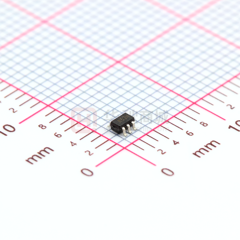
SOT-363
SC-70 (6-LEADS)
S1
1
6
S2
D1
G2
G1
2
5
G2
D2
3
4
S2
G1
Top View
S1
D2
N-Channel
P-Channel
ABSOLUTE MAXIMUM RATINGS TA = 25 °C, unless otherwise noted
N-Channel
Parameter
Symbol
5s
P-Channel
Steady State
5s
Steady State
Drain-Source Voltage
VDS
20
- 20
Gate-Source Voltage
VGS
± 20
± 20
Continuous Drain Current (TJ = 150 °C)a
TA = 25 °C
TA = 85 °C
Pulsed Drain Current
IS
TA = 25 °C
TA = 85 °C
Operating Junction and Storage Temperature Range
PD
V
3.28
3.03
- 2.80
- 2.58
2.12
1.81
- 1.72
- 1.53
9.5
IDM
Continuous Source Current (Diode Conduction)a
Maximum Power Dissipationa
ID
- 8.5
2.61
2.48
- 1.61
-1.48
1.24
1.17
1.10
0.97
0.88
0.75
0.66
0.5
TJ, Tstg
Unit
- 55 to 150
A
W
°C
THERMAL RESISTANCE RATINGS
Parameter
Maximum Junction-to-Ambienta
Maximum Junction-to-Foot (Drain)
Symbol
t≤5s
Steady State
Steady State
RthJA
RthJF
Typical
Maximum
130
170
170
220
80
100
Unit
°C/W
Notes:
a. Surface mounted on 1" x 1" FR4 board.
服务热线:400-655-8788
1
�Si1553CDL-T1-GE3
www.VBsemi.com
SPECIFICATIONS TJ = 25 °C, unless otherwise noted
Parameter
Symbol
Test Conditions
Min.
Typ.
Max.
Unit
Static
Gate Threshold Voltage
Gate-Body Leakage
VGS(th)
VDS = VGS, ID = 100 µA
N-Ch
0.45
1
VDS = VGS, ID = - 100 µA
P-Ch
- 0.45
1
N-Ch
± 100
P-Ch
± 100
N-Ch
1
VDS = - 16 V, VGS = 0 V
P-Ch
-1
VDS = 16 V, VGS = 0 V, TJ = 85 °C
N-Ch
5
IGSS
VDS = 0 V, VGS = ± 8 V
VDS = 16 V, VGS = 0 V
Zero Gate Voltage Drain Current
On-State Drain Currenta
Drain-Source On-State Resistancea
Forward Transconductancea
Diode Forward Voltagea
IDSS
P-Ch
VDS ≥ 5 V, VGS = 4.5 V
N-Ch
2
VDS ≤ - 5 V, VGS = - 4.5 V
P-Ch
-2
RDS(on)
gfs
VSD
nA
µA
-5
VDS = - 16 V, VGS = 0 V, TJ = 85 °C
ID(on)
V
A
VGS = 4.5 V, ID = 2.55 A
N-Ch
0.090
VGS = - 4.5 V, ID = - 1.85 A
P-Ch
0.155
VGS = 2.5 V, ID = 1.55 A
N-Ch
0.110
VGS = - 2.5 V, ID = - 1.35 A
P-Ch
0.19+0
VGS = 1.8 V, ID = 0.50 A
N-Ch
0.130
VGS = - 1.8 V, ID = - 0.50 A
P-Ch
0.220
VDS = 10 V, ID = 1.13 A
N-Ch
2.6
VDS = - 10 V, ID = - 0.88 A
P-Ch
1.5
IS = 0.48 A, VGS = 0 V
N-Ch
0.8
1.2
IS = - 0.48 A, VGS = 0 V
P-Ch
- 0.8
- 1.2
N-Ch
1.25
2
1.8
Ω
S
V
Dynamicb
Total Gate Charge
Qg
Gate-Source Charge
Qgs
Gate-Drain Charge
Qgd
Turn-On Delay Time
td(on)
Rise Time
Turn-Off Delay Time
tr
td(off)
Fall Time
tf
Reverse Recovery Time
trr
N-Channel
VDS = 10 V, VGS = 4.5 V, ID = 2.55 A
P-Channel
VDS = - 10 V, VGS = - 4.5 V, ID = - 0.88
A
N-Channel
VDD = 10 V, RL = 20 Ω
ID ≅ 0.5 A, VGEN = 4.5 V, Rg = 6 Ω
P-Channel
VDD = - 10 V, RL = 20 Ω
ID ≅ - 0.5 A, VGEN = - 4.5 V, Rg = 6 Ω
IF = 0.48 A, dI/dt = 100 A/µs
P-Ch
1.2
N-Ch
0.21
P-Ch
0.3
N-Ch
0.3
P-Ch
0.21
nC
N-Ch
15
25
P-Ch
18
30
N-Ch
22
35
P-Ch
25
40
N-Ch
25
40
P-Ch
15
25
N-Ch
12
20
P-Ch
12
20
N-Ch
30
60
P-Ch
30
60
ns
Notes:
a. Pulse test; pulse width ≤ 300 µs, duty cycle ≤ 2 %.
b. Guaranteed by design, not subject to production testing.
Stresses beyond those listed under “Absolute Maximum Ratings” may cause permanent damage to the device. These are stress ratings only, and functional operation
of the device at these or any other conditions beyond those indicated in the operational sections of the specifications is not implied. Exposure to absolute maximum
rating conditions for extended periods may affect device reliability.
2
服务热线:400-655-8788
�Si1553CDL-T1-GE3
www.VBsemi.com
N-CHANNEL TYPICAL CHARACTERISTICS 25 °C, unless otherwise noted
10
10
VGS = 5 V thru3 V
TC = - 55 °C
I D - Drain Current (A)
I D - Drain Current (A)
25 °C
7.5
1.5 V
5.0
2.5
7.5
125 °C
5.0
2.5
1V
0.0
0
1
2
3
0.0
0.0
4
0.5
1.0
2.0
1.5
VGS - Gate-to-Source Voltage (V)
VDS - Drain-to-Source Voltage (V)
Output Characteristics
Transfer Characteristics
0.6
160
120
C - Capacitance (pF)
RDS(on) - On-Resistance (Ω)
0.5
0.4
0.3
VGS = 1.8 V
0.2
VGS = 2.5 V
Ciss
80
40
Coss
0.1
VGS = 4.5 V
0.0
0.0
Crss
0
0.5
1.0
1.5
2.0
0
4
ID - Drain Current (A)
8
20
VDS - Drain-to-Source Voltage (V)
On-Resistance vs. Drain Current
Capacitance
5
1.6
VDS = 10 V
ID = 1.28 A
VGS = 4.5 V
ID = 1.13 A
4
1.4
R DS(on) - On-Resistance
(Normalized)
VGS - Gate-to-Source Voltage (V)
16
12
3
2
1
0
0.0
1.2
1.0
0.8
0.3
0.6
0.9
Qg - Total Gate Charge (nC)
Gate Charge
1.2
1.5
0.6
- 50
- 25
0
25
50
75
100
125
150
TJ - Junction Temperature (°C)
On-Resistance vs. Junction Temperature
服务热线:400-655-8788
3
�Si1553CDL-T1-GE3
www.VBsemi.com
N-CHANNEL TYPICAL CHARACTERISTICS 25 °C, unless otherwise noted
0.6
2
TJ = 150 °C
R DS(on) - On-Resistance (Ω)
0.5
I S - Source Current (A)
1
TJ = 25 °C
0.4
ID = 1.13 A
0.3
0.2
0.1
0.0
0.1
0
0.4
0.2
0.6
0.8
1.0
0
1.2
1
3
4
5
VGS - Gate-to-Source Voltage (V)
VSD - Source-to-Drain Voltage (V)
On-Resistance vs. Gate-to-Source Voltage
Source-Drain Diode Forward Voltage
0.2
5
ID = 100 µA
0.1
4
0.0
3
Power (W)
VGS(th) Variance (V)
2
- 0.1
2
- 0.2
1
- 0.3
- 0.4
- 50
- 25
0
25
50
75
100
125
0
0.01
150
0.1
1
10
100
600
TJ - Temperature (°C)
Time (s)
Threshold Voltage
Single Pulse Power, Junction-to-Ambient
10
IDM Limited
P(t) = 0.0001
I D - Drain Current (A)
Limited by RDS(on)*
1
P(t) = 0.001
ID(on)
Limited
P(t) = 0.01
0.1
P(t) = 0.1
TA = 25 °C
Single Pulse
P(t) = 1
P(t) = 10, DC
BVDSS Limited
0.01
0.1
1
10
100
V DS - Drain-to-Source Voltage (V)
* V GS > minimum VGS at which RDS(on) is specified
Safe Operating Area, Junction-to-Ambient
4
服务热线:400-655-8788
�Si1553CDL-T1-GE3
www.VBsemi.com
N-CHANNEL TYPICAL CHARACTERISTICS 25 °C, unless otherwise noted
2
Normalized Effective Transient
Thermal Impedance
1
Duty Cycle = 0.5
0.2
Notes:
0.1
PDM
0.1
0.05
t1
t2
1. Duty Cycle, D =
0.02
t1
t2
2. Per Unit Base = R thJA = 170 °C/W
3. T JM - TA = PDMZthJA(t)
Single Pulse
0.01
10-4
4. Surface Mounted
10-3
10-2
10-1
1
10
100
600
Square Wave Pulse Duration (s)
Normalized Thermal Transient Impedance, Junction-to-Ambient
2
Normalized Effective Transient
Thermal Impedance
1
Duty Cycle = 0.5
0.2
0.1
0.1
0.05
0.02
Single Pulse
0.01
10-4
10-3
10-2
10-1
1
10
Square Wave Pulse Duration (s)
Normalized Thermal Transient Impedance, Junction-to-Foot
服务热线:400-655-8788
5
�Si1553CDL-T1-GE3
www.VBsemi.com
P-CHANNEL TYPICAL CHARACTERISTICS 25 °C, unless otherwise noted
3.0
3.0
TC = - 55 °C
2.5
I D - Drain Current (A)
I D - Drain Current (A)
2.5
3V
VGS = 5 V
thru 3.5 V
2.5 V
2.0
1.5
2V
1.0
1.5 V
0.5
25 °C
2.0
125 °C
1.5
1.0
0.5
1V
0.0
0.0
0.0
0
1
2
3
4
0.5
1.0
1.5
3.0
3.5
VGS - Gate-to-Source Voltage (V)
VDS - Drain-to-Source Voltage (V)
Output Characteristics
Transfer Characteristics
160
0.64
VGS = 1.8 V
Ciss
120
0.48
C - Capacitance (pF)
R DS(on) - On-Resistance (Ω)
2.5
2.0
VGS = 2.5 V
0.32
VGS = 4.5 V
80
Coss
40
0.16
Crss
0.0
0.0
0
0.5
1.0
1.5
2.0
2.5
0
3.0
8
10
VDS - Drain-to-Source Voltage (V)
Capacitance
12
1.6
VGS = 4.5 V
ID = 0.88 A
1.4
3
2
(Normalized)
4
R DS(on) - On-Resistance
VGS - Gate-to-Source Voltage (V)
6
ID - Drain Current (A)
VDS = 10 V
ID = 0.9 A
6
4
On-Resistance vs. Drain Current
5
1.2
1.0
0.8
1
0
0.0
2
0.3
0.6
0.9
1.2
1.5
0.6
- 50
- 25
0
25
50
75
100
125
Qg - Total Gate Charge (nC)
TJ - Junction Temperature (°C)
Gate Charge
On-Resistance vs. Junction Temperature
150
服务热线:400-655-8788
�Si1553CDL-T1-GE3
www.VBsemi.com
P-CHANNEL TYPICAL CHARACTERISTICS 25 °C, unless otherwise noted
1.6
2
I S - Source Current (A)
ID = 0.88 A
R DS(on) - On-Resistance (Ω)
TJ = 150 °C
1
TJ = 25 °C
1.2
0.8
0.4
0.0
0.1
0
0.4
0.2
0.6
0.8
1.0
0
1.2
1
2
3
4
5
VGS - Gate-to-Source Voltage (V)
VSD - Source-to-Drain Voltage (V)
On-Resistance vs. Gate-to-Source Voltage
Source-Drain Diode Forward Voltage
0.30
5
0.25
ID = 100 µA
4
0.15
3
Power (W)
V GS(th) Variance (V)
0.20
0.10
0.05
2
0.00
- 0.05
1
- 0.10
- 0.15
- 50
- 25
0
25
50
75
100
125
0
0.01
150
0.1
1
10
100
TJ - Temperature (°C)
Time (s)
Threshold Voltage
Single Pulse Power, Junction-to-Ambient
600
10
IDM Limited
I D - Drain Current (A)
P(t) = 0.0001
Limited by RDS(on)*
1
P(t) = 0.001
ID(on)
Limited
P(t) = 0.01
0.1
P(t) = 0.1
TA = 25 °C
Single Pulse
BVDSS Limited
0.01
0.1
1
P(t) = 1
P(t) = 10
DC
10
100
VDS - Drain-to-Source Voltage (V)
* VGS > minimum VGS at which R DS(on) is specified
Safe Operating Area, Junction-to-Ambient
服务热线:400-655-8788
7
�Si1553CDL-T1-GE3
www.VBsemi.com
P-CHANNEL TYPICAL CHARACTERISTICS 25 °C, unless otherwise noted
2
Normalized Effective Transient
Thermal Impedance
1
Duty Cycle = 0.5
0.2
Notes:
0.1
PDM
0.1
0.05
t1
t2
1. Duty Cycle, D =
2. Per Unit Base = R thJA = 170 °C/W
0.02
3. T JM - TA = PDMZthJA(t)
Single Pulse
0.01
10-4
t1
t2
4. Surface Mounted
10-3
10-2
10-1
1
10
100
600
Square Wave Pulse Duration (s)
Normalized Thermal Transient Impedance, Junction-to-Ambient
Normalized Effective Transient
Thermal Impedance
2
1
Duty Cycle = 0.5
0.2
0.1
0.1
0.05
0.02
Single Pulse
0.01
10-4
10-3
10-2
10-1
1
10
Square Wave Pulse Duration (s)
Normalized Thermal Transient Impedance, Junction-to-Foot
8
服务热线:400-655-8788
�Si1553CDL-T1-GE3
SCĆ70:
www.VBsemi.com
6ĆLEADS
MILLIMETERS
6
5
Dim
A
A1
A2
b
c
D
E
E1
e
e1
L
4
E1 E
1
2
3
-B-
e
b
e1
D
-Ac
A2 A
L
INCHES
Min
Nom
Max
Min
Nom
Max
0.90
–
1.10
0.035
–
0.043
–
–
0.10
–
–
0.004
0.80
–
1.00
0.031
–
0.039
0.15
–
0.30
0.006
–
0.012
0.10
–
0.25
0.004
–
0.010
1.80
2.00
2.20
0.071
0.079
0.087
1.80
2.10
2.40
0.071
0.083
0.094
1.15
1.25
1.35
0.045
0.049
0.053
0.65BSC
0.026BSC
1.20
1.30
1.40
0.047
0.051
0.055
0.10
0.20
0.30
0.004
0.008
0.012
7_Nom
7_Nom
A1
服务热线:400-655-8788
9
�Si1553CDL-T1-GE3
www.VBsemi.com
Disclaimer
All products due to improve reliability, function or design or for other reasons, product specifications and
data are subject to change without notice.
Taiwan VBsemi Electronics Co., Ltd., branches, agents, employees, and all persons acting on its or their
representatives (collectively, the "Taiwan VBsemi"), assumes no responsibility for any errors, inaccuracies or
incomplete data contained in the table or any other any disclosure of any information related to the
product.(www.VBsemi.com)
Taiwan VBsemi makes no guarantee, representation or warranty on the product for any particular purpose of
any goods or continuous production. To the maximum extent permitted by applicable law on Taiwan VBsemi
relinquished: (1) any application and all liability arising out of or use of any products; (2) any and all liability,
including but not limited to special, consequential damages or incidental ; (3) any and all implied warranties,
including a particular purpose, non-infringement and merchantability guarantee.
Statement on certain types of applications are based on knowledge of the product is often used in a typical
application of the general product VBsemi Taiwan demand that the Taiwan VBsemi of. Statement on whether the
product is suitable for a particular application is non-binding. It is the customer's responsibility to verify specific
product features in the products described in the specification is appropriate for use in a particular application.
Parameter data sheets and technical specifications can be provided may vary depending on the application and
performance over time. All operating parameters, including typical parameters must be made by customer's
technical experts validated for each customer application. Product specifications do not expand or modify Taiwan
VBsemi purchasing terms and conditions, including but not limited to warranty herein.
Unless expressly stated in writing, Taiwan VBsemi products are not intended for use in medical, life saving,
or life sustaining applications or any other application. Wherein VBsemi product failure could lead to personal
injury or death, use or sale of products used in Taiwan VBsemi such applications using client did not express their
own risk. Contact your authorized Taiwan VBsemi people who are related to product design applications and
other terms and conditions in writing.
The information provided in this document and the company's products without a license, express or implied,
by estoppel or otherwise, to any intellectual property rights granted to the VBsemi act or document. Product
names and trademarks referred to herein are trademarks of their respective representatives will be all.
Material Category Policy
Taiwan VBsemi Electronics Co., Ltd., hereby certify that all of the products are determined to be
oHS compliant and meets the definition of restrictions under Directive of the European Parliament
2011/65 / EU, 2011 Nian. 6. 8 Ri Yue restrict the use of certain hazardous substances in electrical and
electronic equipment (EEE) - modification, unless otherwise specified as inconsistent.(www.VBsemi.com)
Please note that some documents may still refer to Taiwan VBsemi RoHS Directive 2002/95 / EC. We
confirm that all products identified as consistent with the Directive 2002/95 / EC European Directive
2011/65 /.
Taiwan VBsemi Electronics Co., Ltd. hereby certify that all of its products comply identified as
halogen-free halogen-free standards required by the JEDEC JS709A. Please note that some Taiwanese
VBsemi documents still refer to the definition of IEC 61249-2-21, and we are sure that all products
conform to confirm compliance with IEC 61249-2-21 standard level JS709A.
�


 工商网监
湘ICP备2023018690号
工商网监
湘ICP备2023018690号
