NSi8120/NSi8121/NSi8122: High Reliability
Dual-Channel Digital Isolators
Datasheet (EN) 1.8
Safety Regulatory Approvals
EN
TI
The NSi812x devices are high reliability dual-channel
digital isolator. The NSi812x device is safety certified by
UL1577 support several insulation withstand voltages
(3.75kVrms, 5kVrms), while providing high electromagnetic
immunity and low emissions at low power consumption.
The data rate of the NSi812x is up to 150Mbps, and the
common-mode transient immunity (CMTI) is up to
150kV/us. The NSi812x device provides digital channel
direction configuration and the default output level
configuration when the input power is lost. Wide supply
voltage of the NSi812x device support to connect with
most digital interface directly, easy to do the level shift.
High system level EMC performance enhance reliability
and stability of use. AEC-Q100 (Grade 1) option is
provided for all devices.
AL
Product Overview
Key Features
UL recognition: up to 5000Vrms for 1 minute per UL1577
CQC certification per GB4943.1-2011
CSA component notice 5A
DIN VDE V 0884-11:2017-01
ID
Applications
Up to 5000Vrms Insulation voltage
Date rate: DC to 150Mbps
NF
Power supply voltage: 2.5V to 5.5V
All devices are AEC-Q100 qualified
High CMTI: 150kV/us
Chip level ESD: HBM: ±6kV
Industrial automation system
Isolated SPI, RS232, RS485
General-purpose multichannel isolation
Motor control
Functional Block Diagrams
CO
High system level EMC performance:
Enhanced system level ESD, EFT, Surge immunity
Default output high level or low level option
VDD1 1
8 VDD2
VDD1 1
8 VDD2
INA 2
7 OUTA
OUTA 2
7 INA
INB 3
6 OUTB
INB 3
5 GND2
GND1 4
GND1 4
NSi8120
Isolation barrier life: >60 years
Low power consumption: 1.5mA/ch (1 Mbps)
Low propagation delay: 400
um
Distance through insulation
V
DIN EN 60112 (VDE 0303-11);
IEC 60112
EN
TI
Minimum internal gap
AL
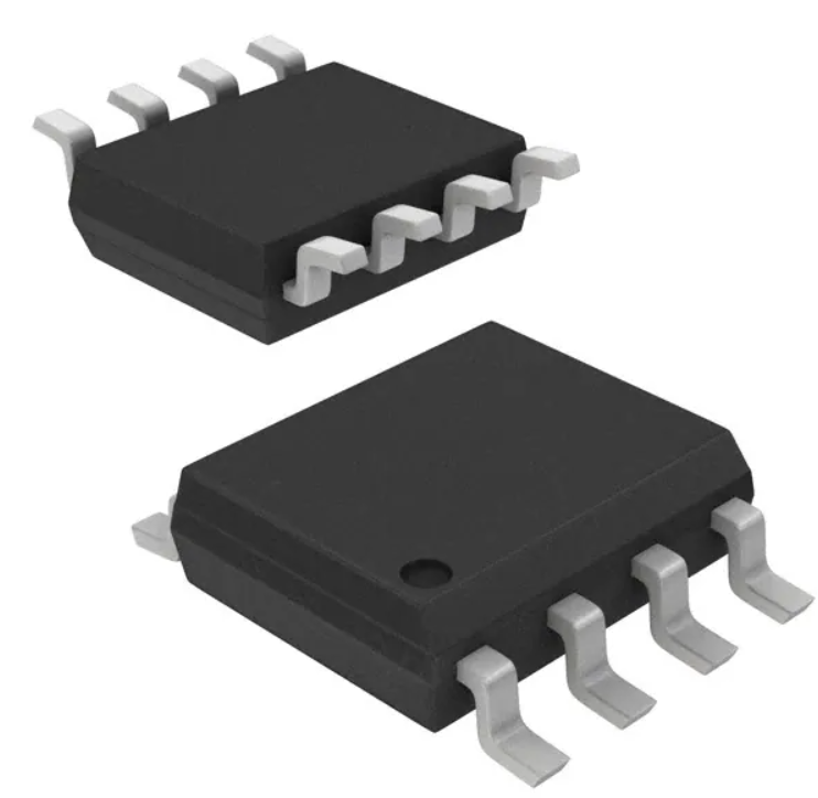
SOIC-8
Material Group
Ⅱ
3.2. DIN VDE V 0884-11(VDE V 0884-11):2017-01 INSULATION CHARATERISTICS
Description
Test Condition
Symbol
Value
SOIC-16
For Rated Mains Voltage ≤ 150Vrms
Ⅰto Ⅳ
Ⅰto Ⅳ
Ⅰto Ⅲ
Ⅰto Ⅳ
For Rated Mains Voltage ≤ 400Vrms
Ⅰto Ⅲ
Ⅰto Ⅳ
ID
SOIC-8
Unit
NF
Installation Classification per DIN VDE
0110
For Rated Mains Voltage ≤ 300Vrms
CO
Climatic Classification
10/105/21
Pollution Degree per DIN VDE 0110,
2
10/105/2
1
2
Table 1
Maximum repetitive isolation voltage
Input to Output Test Voltage, Method
B1
V IORM × 1.5 = V pd (m) , 100%
production test,
VIORM
565
849
Vpeak
V pd (m)
847
1273
Vpeak
V pd (m)
678
1018
Vpeak
t ini = t m = 1 sec, partial
discharge < 5 pC
Input to Output Test Voltage, Method A
After Environmental Tests Subgroup 1
Copyright © 2019, NOVOSENSE
V IORM × 1.2= V pd (m) , t ini = 60
sec, t m = 10 sec, partial
discharge < 5 pC
Page 9
�NSi8120/NSi8121/NSi8122
Test
V IORM × 1.2= V pd (m) , t ini = 60
sec, t m = 10 sec, partial
discharge < 5 pC
V pd (m)
678
1018
Vpeak
t = 60 sec
VIOTM
5300
7000
Vpeak
Test method per
IEC60065,1.2/50us
waveform,
VTEST=VIOSM×1.3
VIOSM
5384
5384
Vpeak
VIO =500V
RIO
>109
>109
Ω
Maximum transient isolation voltage
Maximum Surge Isolation Voltage
Isolation resistance
Isolation capacitance
AL
After Input and /or Safety
Subgroup 2 and Subgroup 3
f = 1MHz
Input capacitance
CIO
0.6
CI
2
Ps
EN
TI
Total Power Dissipation at 25℃
θJA = 140 °C/W, V I = 5.5 V,
T J = 150 °C, T A = 25 °C
Safety input, output, or supply current
Is
2
pF
1499
mW
150
mA
237
mA
150
℃
CO
NF
ID
Saftey Limiting Current (mA)
Ts
180
160
140
120
100
80
60
40
20
0
pF
160
θJA = 84 °C/W, V I = 5.5 V, T
J = 150 °C, T A = 25 °C
Case Temperature
0.6
0
50
100
150
200
Case Temperature (℃)
Figure 3.1 NSi8120N/NSi8121N/NSi8122N Thermal Derating Curve, Dependence of Safety Limiting Values with Case Temperature per DIN VDE V 0884-11
Saftey Limiting Current
(mA)
250
200
150
100
50
0
0
50
100
150
200
Case Temperature (℃)
Figure 3.2 NSi8120W/NSi8121W/NSi8122W Thermal Derating Curve, Dependence of Safety Limiting Values with Case Temperature per DIN VDE V 0884-11
Copyright © 2019, NOVOSENSE
Page 10
�NSi8120/NSi8121/NSi8122
3.3. REGULATORY INFORMATION
The NSi8120N/NSi8121N/NSi8122N are approved by the organizations listed in table.
CUL
UL 1577 Component
Recognition Program1
VDE
Approved under CSA Component
Acceptance Notice 5A
DIN VDE V 088411:2017-012
CQC
Certified by CQC11471543-2012
GB4943.1-2011
Single Protection, 3750Vrms Isolation
voltage
File (E500602)
1
File (E500602)
Basic Insulation
565Vpeak,
VIOSM=5384Vpeak
Basic insulation at
400Vrms (565Vpeak)
AL
Single Protection, 3750Vrms
Isolation voltage
File (5024579-48800001)
File (pending)
In accordance with UL 1577, each NSi8120N/NSi8121N/NSi8122N is proof tested by applying an insulation test voltage ≥ 4500 V rms for 1 sec.
2
EN
TI
In accordance with DIN VDE V 0884-11, each NSi8120N/NSi8121N/NSi8122N is proof tested by applying an insulation test voltage ≥ 847 V peak for 1 sec
(partial discharge detection limit = 5 pC). The * marking branded on the component designates DIN VDE V 0884-11 approval.
The NSi8120W/NSi8121W/NSi8122W are approved by the organizations listed in table.
CUL
UL 1577 Component Recognition
Program1
DIN VDE V 088411(VDE V 088411):2017-012
Certified by CQC11471543-2012
Single Protection, 5000Vrms
Isolation voltage
Basic Insulation
849Vpeak,
VIOSM=5384Vpeak
Basic insulation at
800Vrms (1131Vpeak)
File (E500602)
NF
File (E500602)
1
CQC
Approved under CSA
Component Acceptance Notice
5A
ID
Single Protection, 5000Vrms Isolation
voltage
VDE
File (5024579-48800001)
GB4943.1-2011
Reinforced insulation at
400Vrms (565Vpeak)
File (pending)
In accordance with UL 1577, each NSi8120W/NSi8121W/NSi8122W is proof tested by applying an insulation test voltage ≥ 6000 V rms for 1 sec.
2
CO
In accordance with DIN VDE V 0884-11, each NSi8120W/NSi8121W/NSi8122W is proof tested by applying an insulation test voltage ≥ 1273 V peak for 1 sec
(partial discharge detection limit = 5 pC). The * marking branded on the component designates DIN VDE V 0884-11 approval.
4.0
FUNCTION DESCRIPTION
The NSi812x is a Dual-channel digital isolator based on a capacitive isolation barrier technique. The digital signal is modulated with RF
carrier generated by the internal oscillator at the Transmitter side. Then it is transferred through the capacitive isolation barrier and
demodulated at the Receiver side.
The NSi812x devices are high reliability dual-channel digital isolator with AEC-Q100 qualified. The NSi812x device is safety certified by
UL1577 support several insulation withstand voltages (3.75kVrms, 5kVrms), while providing high electromagnetic immunity and low
emissions at low power consumption. The data rate of the NSi812x is up to 150Mbps, and the common-mode transient immunity
(CMTI) is up to 150kV/us. The NSi812x device provides digital channel direction configuration and the default output level
configuration when the input power is lost. Wide supply voltage of the NSi812x device support to connect with most digital interface
directly, easy to do the level shift. High system level EMC performance enhance reliability and stability of use.
The NSi812x has a default output status when VDDIN is unready and VDDOUT is ready as shown in Table 4.1, which helps for diagnosis
when power is missing at the transmitter side. The output B follows the same status with the input A within 1us after powering up.
Copyright © 2019, NOVOSENSE
Page 11
�NSi8120/NSi8121/NSi8122
Table 4.1 Output status vs. power status
Input
VDD1
status
VDD2
status
Output
Comment
H
Ready
Ready
H
Normal operation.
L
Ready
Ready
L
X
Unready
Ready
L
The output follows the same status with the input within 60us after
input side VDD1 is powered on.
H
Unready
X
The output follows the same status with the input within 60us after
output side VDD2 is powered on.
AL
5.0
Ready
APPLICATION NOTE
EN
TI
X
5.1. PCB LAYOUT
The NSi812x requires a 0.1 µF bypass capacitor between VDD1 and GND1, VDD2 and GND2. The capacitor should be
placed as close as possible to the package. Figure 5.1 to Figure 5.4 show the recommended PCB layout, make sure the space under the
chip should keep free from planes, traces, pads and via. To enhance the robustness of a design, the user may also include resistors
(50–300 Ω ) in series with the inputs and outputs if the system is excessively noisy. The series resistors also improve the system
reliability such as latch-up immunity.
NF
ID
The typical output impedance of an isolator driver channel is approximately 50 Ω, ±40%. When driving loads where transmission line
effects will be a factor, output pins should be appropriately terminated with controlled impedance PCB traces.
Figure5.2 Recommended PCB Layout — Bottom Layer
CO
Figure5.1 Recommended PCB Layout — Top Layer
Figure5.3 Recommended PCB Layout — Top Layer
Figure5.4 Recommended PCB Layout — Bottom Layer
5.2. HIGH SPEED PERFORMANCE
Figure 5.5 shows the eye diagram of NSi812x at 200Mbps data rate output. The result shows a typical measurement on the NSi812x
with 350ps p-p jitter.
Copyright © 2019, NOVOSENSE
Page 12
�EN
TI
AL
NSi8120/NSi8121/NSi8122
Figure5.5 NSi812x Eye Diagram
5.3. TYPICAL SUPPLY CURRENT EQUATIONS
The typical supply current of NSi812x can be calculated using below equations. IDD1 and IDD2 are typical supply currents measured in
mA, f is data rate measured in Mbps, CL is the capacitive load measured in pF
NSi8120:
ID
IDD1 = 0.19 *a1+1.45*b1+0.82*c1.
IDD2 = 1.36+ VDD1*f* CL *c1*10-9
When a1 is the channel number of low input at side 1, b1 is the channel number of high input at side 1, c1 is the channel number of
switch signal input at side 1.
NF
NSi8121/ NSi8122:
IDD1 = 0.87 +1.26*b1+0.63*c1+ VDD1*f* CL *c2*10-9
IDD2 = 0.87 +1.26*b2+0.63*c2+ VDD1*f* CL *c1*10-9
When b1 is the channel number of high input at side 1, c1 is the channel number of switch signal input at side 1, b2 is the channel
number of high input at side 2, c2 is the channel number of switch signal input at side 2.
PACKAGE INFORMATION
CO
6.0
VDD1 1
8 VDD2
VDD1 1
8 VDD2
INA 2
7 OUTA
OUTA 2
7 INA
INB 3
6 OUTB
INB 3
5 GND2
GND1 4
GND1 4
NSi8120
Figure 6.1 NSi8120N Package
Copyright © 2019, NOVOSENSE
6 OUTB
NSi8121
5 GND2
Figure 6.2 NSi8121N Package
Page 13
�NSi8120/NSi8121/NSi8122
VDD1 1
8 VDD2
INA 2
7 OUTA
OUTB 3
GND1 4
6 INB
NSi8122
5 GND2
ID
EN
TI
AL
Figure 6.3 NSi8122N Package
Figure 6.4 SOIC8 Package Shape and Dimension in millimeters (inches)
Table6.1 NSi8120N/ NSi8121N/ NSi8122N Pin Configuration and Description
NSi8121N
PIN NO.
NSi8122N
PIN NO.
SYMBOL
FUNCTION
1
1
1
VDD1
Power Supply for Isolator Side 1
7
2
INA
Logic Input A
3
6
INB
Logic Input B
4
4
4
GND1
Ground 1, the ground reference for Isolator Side 1
5
5
5
GND2
Ground 2, the ground reference for Isolator Side 2
6
6
3
OUTB
Logic Output B
7
2
7
OUTA
Logic Output A
8
8
8
VDD2
Power Supply for Isolator Side 2
2
CO
3
NF
NSi8120N
PIN NO.
Copyright © 2019, NOVOSENSE
Page 14
�NSi8120/NSi8121/NSi8122
GND1 1
16 GND2
NC 2
15 NC
GND1 1
16 GND2
NC 2
15 NC
VDD1 3
14 VDD2
VDD1 3
14 VDD2
INA 4
13 OUTA
OUTA 4
13 INA
INB 5
12 OUTB
INB 5
NC 6
11 NC
NC 6
11 NC
GND1 7
10 NC
GND1 7
10 NC
NSi8120
9 GND2
NC 8
NSi8121
9
GND2
Figure 6.6 NSi8121W Package
EN
TI
Figure 6.5 NSi8120W Package
AL
NC 8
12 OUTB
GND1 1
16 GND2
NC 2
15 NC
VDD1 3
14 VDD2
INA 4
13 OUTA
12 INB
NC 6
11 NC
GND1 7
10 NC
ID
OUTB 5
NSi8122
9 GND2
NF
NC 8
CO
Figure 6.7 NSi8122W Package
Figure 6.8 WB SOIC16 Package Shape and Dimension in millimeters and (inches)
Copyright © 2019, NOVOSENSE
Page 15
�NSi8120/NSi8121/NSi8122
Table 6.2 NSi8120W/ NSi8121W/ NSi8122W Pin Configuration and Description
NSi8121W
PIN NO.
NSi8122W
PIN NO.
SYMBOL
FUNCTION
1
1
1
GND1
Ground 1, the ground reference for Isolator Side 1
2
2
2
NC
No Connection.
3
3
3
VDD1
Power Supply for Isolator Side 1
4
13
4
INA
Logic Input A
5
5
12
INB
6
6
6
NC
7
7
7
GND1
8
8
8
9
9
9
10
10
10
11
11
11
12
12
5
13
4
13
14
14
15
15
16
16
AL
NSi8120W
PIN NO.
Logic Input B
No Connection.
EN
TI
Ground 1, the ground reference for Isolator Side 1
No Connection.
GND2
Ground 2, the ground reference for Isolator Side 2
NC
No Connection.
NC
No Connection.
OUTB
Logic Output A
OUTA
Logic Output B
ID
NC
VDD2
Power Supply for Isolator Side 2
15
NC
No Connection.
16
GND2
Ground 2, the ground reference for Isolator Side 2
CO
NF
14
Copyright © 2019, NOVOSENSE
Page 16
�NSi8120/NSi8121/NSi8122
TAPE AND REEL INFORMATION
CO
NF
ID
EN
TI
AL
7.0
Copyright © 2019, NOVOSENSE
Page 17
�EN
TI
AL
NSi8120/NSi8121/NSi8122
CO
NF
ID
Figure 7.1 Tape and Reel Information of SOIC8
Copyright © 2019, NOVOSENSE
Page 18
�CO
NF
ID
EN
TI
AL
NSi8120/NSi8121/NSi8122
Figure 7.2 Tape and Reel Information of WB SOIC16
Copyright © 2019, NOVOSENSE
Page 19
�NSi8120/NSi8121/NSi8122
8.0
ORDER INFORMATION
Part No.
Isolation
Rating(kV)
Number
of side 1
inputs
Number
of side 2
inputs
Max Data
Rate
(Mbps)
Default
Output
State
Temperature
Automotive
Package
NF
ID
EN
TI
AL
NSi8120N0
3.75
2
0
150
Low
NO
SOIC8
-40 to 125℃
NSi8120N1
3.75
2
0
150
High
NO
SOIC8
-40 to 125℃
NSi8121N0
3.75
1
1
150
Low
NO
SOIC8
-40 to 125℃
NSi8121N1
3.75
1
1
150
High
NO
SOIC8
-40 to 125℃
NSi8122N0
3.75
1
1
150
Low
NO
SOIC8
-40 to 125℃
NSi8122N1
3.75
1
1
150
High
NO
SOIC8
-40 to 125℃
NSi8120W0
5
2
0
150
Low
NO
WB SOIC16
-40 to 125℃
NSi8120W1
5
2
0
150
High
NO
WB SOIC16
-40 to 125℃
NSi8121W0
5
1
1
150
Low
NO
WB SOIC16
-40 to 125℃
NSi8121W1
5
1
1
150
High
NO
WB SOIC16
-40 to 125℃
NSi8122W0
5
1
1
150
Low
NO
WB SOIC16
-40 to 125℃
NSi8122W1
5
1
1
150
High
NO
WB SOIC16
-40 to 125℃
NSi8120N0Q
3.75
2
0
150
Low
YES
SOIC8
-40 to 125℃
NSi8120N1Q
3.75
2
0
150
High
YES
SOIC8
-40 to 125℃
NSi8121N0Q
3.75
1
1
150
Low
YES
SOIC8
-40 to 125℃
NSi8121N1Q
3.75
1
1
150
High
YES
SOIC8
-40 to 125℃
NSi8122N0Q
3.75
1
1
150
Low
YES
SOIC8
-40 to 125℃
NSi8122N1Q
3.75
1
1
150
High
YES
SOIC8
-40 to 125℃
NSi8120W0Q 5
2
0
150
Low
YES
WB SOIC16
-40 to 125℃
NSi8120W1Q 5
2
0
150
High
YES
WB SOIC16
-40 to 125℃
NSi8121W0Q 5
1
1
150
Low
YES
WB SOIC16
-40 to 125℃
NSi8121W1Q 5
1
1
150
High
YES
WB SOIC16
-40 to 125℃
NSi8122W0Q 5
1
1
150
Low
YES
WB SOIC16
-40 to 125℃
NSi8122W1Q 5
1
1
150
High
YES
WB SOIC16
-40 to 125℃
NOTE: All packages are RoHS-compliant with peak reflow temperatures of 260 °C according to the JEDEC industry standard
classifications and peak solder temperatures.
All devices are AEC-Q100 qualified.
CO
Part Number Rule:
NSi(81)(2)(1)(N)(1)(Q)
Series Number
Total Channel Amount:
N=N Channels N=1,2,4…
N=0: I2C Part
Reverse Channel Amount:
N=N Channels N=0,1,2…
Copyright © 2019, NOVOSENSE
Q = Automotive version
Fail-Safe Output State:
0 = Logic Low
1 = Logic High
Package Type:
N= NB SOIC8
W= WB SOIC16
Page 20
�NSi8120/NSi8121/NSi8122
9.0
REVISION HISTORY
Description
Original
Change to Ordering information
Add maximum operation current specification.
Change block diagram
Correct Table 6.2 Pin No.
Add specification “Input Pull high or low Current”
Date
2017/11/15
2018/3/26
2018/6/20
2018/7/28
2018/8/20
2018/9/10
1.6
Add “Maximum Input/Output Pulse Voltage”
2018/10/9
1.7
1.8
Change to Ordering information
Change Certification Information
AL
Revision
1.0
1.1
1.2
1.3
1.4
1.5
CO
NF
ID
EN
TI
2018/12/20
2019/06/17
Copyright © 2019, NOVOSENSE
Page 21
�


 工商网监
湘ICP备2023018690号
工商网监
湘ICP备2023018690号
