LS7290
July 2011
STEPPER MOTOR CONTROLLER
FEATURES:
•
•
•
•
•
•
•
•
•
•
•
•
•
Controls Bipolar and Unipolar motors
Cost-effective replacement for L297
Full, ½ step mode selected with mode input
Direction control
Reset input
Step control input
Enable input
PWM chopper circuit for current control
Two peak-current comparators with external reference input
Step control frequency and duty cycle controlled by an external frequency source
or by an internal crystal controlled oscillator (typically 8 MHz)
All inputs and outputs TTL/CMOS compatible (TTL for 5V operation)
3V to 5.5V Operation (VDD – VSS)
LS7290 (DIP), LS7290-S (SOIC), LS7290-TS (TSSOP) – See Figure 1.
PIN ASSIGNMENT
TOP VIEW
DESCRIPTION:
The LS7290 generates Phase Drive outputs and PWM outputs for controlling twophase Bipolar Motors or four-phase Unipolar Motors, respectively. The LS7290
contains a mode controlled look-up table for generating the motor duty cycle drive
sequences. There are four outputs which are used to drive two H-Bridges for the two
motor windings in the Bipolar motor or the four driver transistors for the two centertapped windings in the Unipolar motor (Refer to Table 2). The LS7290 can step a
motor in full steps and half steps. The refresh rate is set using an internal oscillator
controlled by a crystal or by use of an external input clock. Typical refresh rate is equal
to 31.25kHz with the clock frequency set at 8MHz. Peak-current feedback control using
pulse-width modulation is used in full-step or half-step modes. The chopper consists of
a voltage comparator, flip-flop and external sense resistor. The internal oscillator sets
the flip-flop and enables the INH1 and INH2 outputs at the beginning of each PWM
cycle. Once the peak motor current causes the voltage across the sense resistors to
reach the voltage set by VREF, the outputs are disabled until the next oscillator pulse.
The VREF voltage sets the peak current in each motor winding.
INPUT/OUTPUT DESCRIPTION
RESET Input
Active low. Resets the PWM table pointer to HOME position per Table 2 and brings
INH1 and INH2 low. Upon power-up, a POR circuit also resets the PWM table pointer.
ENABLE Input
Active low. When high (inactive), brings PHA, PHB, PHC, PHD, INH1 and INH2 outputs
low.
STEP Input
Active low. A low-going pulse on this input causes the motor to advance one step.
7290-072011-1
FIGURE 1.
NOTE: Pins 2 and 3 are used for factory test
and must be tied to ground.
FRD/RVRS Input
A low input causes the motor to move in
incremental steps in reverse direction per Table 2.
A high input causes the motor to move in
incremental steps in forward direction per Table 2.
Switching directions can occur at any time.
MODE Input
Defines the stepping modes as follows:
MODE
full step mode
0
½ step mode
1
Stepping mode can be changed at any time.
SENSE1 / SENSE2 Inputs
Inputs for motor winding current sense. A
fractional-Ohm resistor connected in series with
each of the H-Bridge drivers produce SENSE1 and
SENSE2 voltages. These voltages are compared
with VREF voltage input, for generating the PWM
inhibit outputs.
�VREF Input
External voltage reference for chopper circuit which determines the
maximum motor winding current by regulating the PWM duty cycle. The
SENSE resistors should satisfy the equations RS1 = RS2 = VREF / IMAX
where IMAX is the maximum motor winding current.
RX, CX, CLK
These three pins can be configured in one of three ways to obtain the
primary clock. A crystal connected between RX and CLK pins or a
resistor-capacitor pair connected among all three pins (see Figure 4) can
make use of the internal oscillator. Alternatively, the CLK pin can be
driven from an external clock source.
DS0/DS1 Inputs
The phase drive is blanked out between steps by switching outputs INH1
and INH2 low in order to reduce audible noise and power consumption.
The duration of the blanking is selected by DS0 and DS1 according to
Table 1.
PHA / PHB / PHC / PHD Outputs
The state of these phase outputs are determined by the look-up
table and are used to control either the left or right half of each
of the H-Bridge drivers. A low on a phase output enables the
bottom driver while a high on the output enables the top driver.
HOME Output
Indicates Step0 state per Table 2 with a logic low.
INH1 / INH2 Outputs
These outputs are used to provide PWM control to each of the
two H-Bridge drivers.
The information included herein is believed to be accurate and reliable.
However, LSI Computer Systems, Inc. assumes no responsibilities for
inaccuracies, or for any infringements of patent rights of others which may
result from its use.
Table 1
DS1
0
0
1
1
DS0
0
1
0
1
Blanking Time, IPB, at fc = 8Mz
1.25μs
2.50μs
3.75μs
5.00μs
FIGURE 2. LS7290 BLOCK DIAGRAM
7290-072011-2
�ABSOLUTE MAXIMUM RATINGS:
PARAMETER
DC Supply Voltage
Any Input Voltage
Operating Temperature
Storage Temperature
SYMBOL
VDD - VSS
VIN
TA
TSTG
VALUE
+7
VSS – 0.3 to VDD + 0.3
-20 to +85
-85 to +150
ELECTRICAL SPECIFICATIONS (-25°C < TA < +85°C)
PARAMETER
Supply Voltage
Supply Current
CLK frequency
Enable Propagation Delay
FRD/RVRS Setup Time
(before step pulse)
Step Pulse Width
Interstep Pulse Delay
Interstep Phase Blanking
Reset Pulse Width
Reset to Step Pulse Delay
Hi-Level Input Voltage
Low-Level Input Voltage
High-Level Input Current
Low-Level Input Current
Output Sink Current
Output Source Current
Comparator Offset Voltage
Input Reference Voltage
SYMBOL
VDD
IDD
fc
tepd
MIN
3.0
-
UNIT
V
V
°C
°C
100
TYP
8.0
-
MAX
5.5
2.0
-
UNIT
V
mA
MHz
ns
CONDITIONS
Outputs floating, Inputs high
-
tds
0
-
-
μs
-
SPW
ISD
IPB
RPW
trs
VIH
VIL
IH
IL
IO
IO
IO
IO
VOS
VREF
VREF
1.0
32
1.25
1.0
0
2
-10
-5
5
2.5
0.5
0.5
5
-
5.0
0.8
50
50
15
3.0
1.5
μs
μs
μs
μs
μs
V
V
nA
nA
mA
mA
mA
mA
mV
V
V
at fc = 8 MHz
at fc = 8 MHz
at fc = 8 MHz
at fc = 8 MHz
VDD = 5 ± 0.25V
VDD = 5 ± 0.25V
Leakage Current
Leakage Current
VO = 0.4V, VDD = 5V
VO = 0.4V, VDD = 3.3V
VO = 4V, VDD = 5V
VO = 2.5V, VDD = 3.3V
VREF = 1V
VDD = 5V
VDD = 3.3V
fc ~ 1/5RC
At VDD = 5V and R = 2.2 kΩ, C = 12pF,
oscillator frequency is 8 MHz (typical).
FIGURE 3. RC OSCILLATOR FOR CLOCK GENERATOR
7290-072011-3
�FIGURE 4. PARTIAL SEQUENCE IN FORWARD HALF- STEP MODE
7290-072011-4
�FIGURE 5. TYPICAL APPLICATION SCHEMATIC FOR A TWO PHASE
BIPOLAR MOTOR USING A SINGLE MOTOR IC
7290-072011-5
�FIGURE 6. TYPICAL APPLICATION SCHEMATIC FOR A TWO PHASE
BIPOLAR MOTOR USING TWO SEPARATE MOTOR DRIVER ICs
7290-072011-6
�NOTE: Q1, Q2, Q3, Q4 are MOSFET Power Transistors suitable for 5V Gate Drive
Typical P/Ns = IRLZ44N and IRF3708
FIGURE 7. TYPICAL APPLICATION SCHEMATIC FOR A FOUR PHASE
UNIPOLAR MOTOR USING DISCRETE MOSFET TRANSISTORS
7290-072011-7
�STEP NUMBER
FULL
1/2
0
0
1
1
2
3
2
4
5
3
6
7
0
0
TABLE 2
% DUTY CYCLE
INH1
INH2
PHA
100
0
1
70.7
70.7
1
0
100
0
-70.7
70.7
0
-100
0
0
-70.7
-70.7
0
0
-100
1
70.7
-70.7
1
100
0
1
PHASES
PHB PHC
0
1
0
1
1
1
1
1
1
0
1
0
0
0
0
0
0
1
PHD
0
0
0
0
1
1
1
1
0
STEP ANGLE
HOME
45
90
135
180
225
270
315
HOME
FIGURE 8. Selecting Between Fast and Slow Decay for One Stepper Motor Winding
(Use identical circuit for the other stepper motor winding)
NOTE:
In fast decay mode, inhibit windings are chopped.
In slow decay mode, phase windings are chopped.
NOR Gates: CD4001
7290-072011-8
OR Gates: CD4071
�Z = 10V
Inverters = 74HC04
Gates = 74HC08
Q1 = Q3 = IRF6215 (Typical)
Q2 = Q4 = IRLI3615 (Typical)
FIGURE 9. 120V Motor Discrete Component Driver
7290-072011-9
�
很抱歉,暂时无法提供与“LS7290”相匹配的价格&库存,您可以联系我们找货
免费人工找货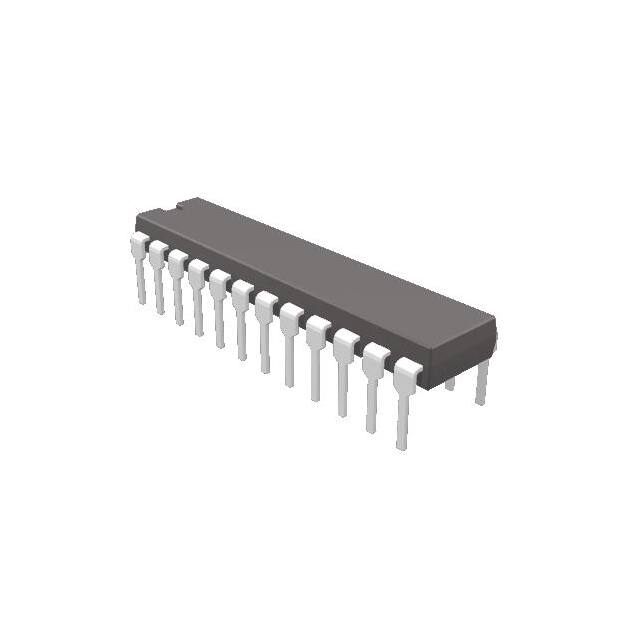


 工商网监
湘ICP备2023018690号
工商网监
湘ICP备2023018690号
