UM4684
0.5Ω Low-Voltage Dual SPDT Analog Switch
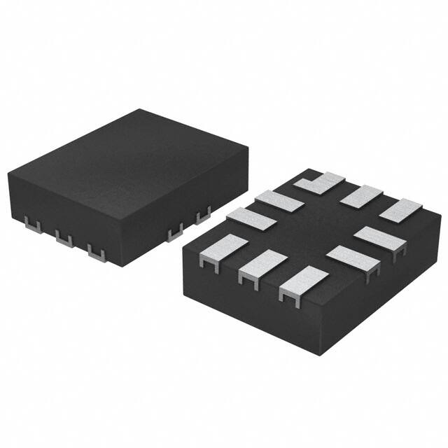
UM4684H CSP10 2.0×1.5
UM4684EEUE MSOP10
General Description
The UM4684 is a sub 1Ω (0.5Ω at 2.7V) dual SPDT analog switch designed for low voltage
applications.
The UM4684 has on-resistance matching(less than 0.05Ω at 2.7V) and flatness (less than 0.2Ω at
2.7V) that are guaranteed over the entire voltage range. Additionally, low logic thresholds make
the UM4684 an ideal interface to low voltage DSP control signals.
The UM4684 has fast switching speed with break-before-make guaranteed. In the ON condition,
all switching elements conduct equally in both directions. OFF-isolation and crosstalk is -69dB at
100kHz.
The UM4684 is built on high-density low voltage CMOS process, and contains the additional
benefit of 2000V ESD protection.
As a committed partner to the community and the environment, Union manufactures this product
with lead (Pb)-free device terminations.
Applications
Features
Cellular Phones
Speaker Headset Switching
Audio and Video Signal Routing
PCMCIA Cards
Battery Operated Systems
Relay Replacement
Power Routing
Communication Circuits
CSP10 & MSOP10 Packages
ESD Protection >2000V
+1.8V to +5.5V Single Supply Operation
NC Switch RON: 0.5Ω (+2.7V Supply)
NO Switch RON: 0.6Ω (+2.7V Supply)
RON Match between Channels: 0.05Ω Max
(+2.7V Supply)
RON Flatness over Signal Range: 0.2Ω Max
(+2.7V Supply)
1.8V Logic Compatibility
Low Crosstalk: -69dB (100kHz)
High Off-Isolation: -69dB (100kHz)
Ordering Information
Part Number
Temp. Range
Packaging Type
Marking Code
UM4684H
-40°C to 85°C
CSP10 2.0×1.5
A
UM4684EEUE
-40°C to 85°C
MSOP10
UM4684EEUE
Shipping Qty
3000pcs/7 Inch
Tape & Reel
4000pcs/13 Inch
Tape & Reel
_______________________________________________________________________
http://www.union-ic.com Rev.11 May.2020
1/12
�UM4684
Pin Configurations
Top View
A
M
(Top View)
M: Month Code
UM4684H
CSP10 2.0×1.5
(Top View)
UM4684
EEUE
XX
XX: Week Code
UM4684EEUE
MSOP10
Ball Mapping for UM4684H
Transparent Top View
_______________________________________________________________________
http://www.union-ic.com Rev.11 May.2020
2/12
�UM4684
Pin Description
Pin
Name
Pin Number
CSP10
MSOP10
2.0×1.5
Function
NC_
A1, C1
5, 7
Analog Switch—Normally Closed Terminal
IN_
A2, C2
4, 8
Digital Control Input
COM_
A3, C3
3, 9
Analog Switch—Common Terminal
NO_
A4, C4
2, 10
Analog Switch—Normally Open Terminal
V+
B4
1
Positive Supply Voltage Input
GND
B1
6
Ground
Function Table
IN_
0
1
NO_
OFF
ON
NC_
ON
OFF
Absolute Maximum Ratings (Note 1)
Parameter
Voltage on V+ Pin (Reference to GND)
Voltage on IN_, COM_, NC_, NO_ Pins (Note 2)
(Reference to GND)
Continuous Current (NO_, NC_, COM_)
Peak Current (Pulsed at 1 ms, 10% Duty Cycle)
Storage Temperature
Package Solder Reflow Conditions IR/Convection
(Note 3)
ESD per Method 3015.7
Power Dissipation (Packages) (Note 4) CSP10 (Note 5)
Value
-0.3 to +6
Unit
V
-0.3 to (V++0.3)
V
±300
±500
-65 to 150
250
>2
457
mA
mA
°C
°C
kV
mW
Note 1: Stresses beyond those listed under “Absolute Maximum Ratings” may cause permanent
damage to the device. These are stress ratings only and functional operation of the device
at these or any other conditions beyond those indicated in the operational sections of the
specifications are not implied. Exposure to absolute maximum rating conditions for
extended periods may affect device reliability.
Note 2: Signals on NC_, NO_, or COM_ or IN_ exceeding V+ will be clamped by internal diodes.
Limit forward diode current to maximum current ratings.
Note 3: Refer to IPC/JEDEC (J-STD-020B).
Note 4: All bumps welded or soldered to PC Board.
Note 5: Derate 5.7mW/°C above 70°C.
_______________________________________________________________________
http://www.union-ic.com Rev.11 May.2020
3/12
�UM4684
Electrical Characteristics (V+=3V, ±10% deviation, VIN=0.5 or 1.4V (Note 6))
Parameter
Symbol
Test Conditions
Otherwise Unless
Specified
Temp
(Note 7)
Limits
(-40°C to 85°C)
Min
Typ
Max
(Note 9) (Note 8) (Note 9)
Unit
Analog Switch
Analog Signal
Range (Note 10)
VNO
VNC
VCOM
Full
On-Resistance
(Note 10)
Ron
Room
Full
RON Flatness
(Note 10)
Ron
Flatness
On-Resistance
Match Between
Channels (Note 10)
ΔRDS(on)
Switch Off Leakage
Current
Channel-On
Leakage Current
INO(off),
INC(off)
ICOM(off)
ICOM(on)
V+=2.7V,
VCOM=0.6/1.5V,
INO, INC=100mA
V+=3.3V,
VNO,VNC=0.3V/3V,
VCOM=3V/0.3V
V+=3.3V,
VNO, VNC=VCOM
=0.3V/3V
0
V+
0.5
V
0.8
1.0
Room
0.15
Room
0.05
Room
Full
-2
-20
2
20
Room
Full
-2
-20
2
20
Room
Full
-2
-20
2
20
1.4
Ω
nA
Digital Control
Input High Voltage
(Note 10)
VINH
Full
Input Low Voltage
VINL
Full
Input Capacitance
CIN
Full
Input Current
IINL
or IINH
VIN=0 or V+
Full
V
0.5
10
-1
pF
1
μA
Dynamic Characteristics
Turn-On Time
tON
VNO or VNC=2.0V,
RL=50Ω, CL=35pF
Room
Full
Room
Full
Turn-Off Time
tOFF
Break-Before-Make
Time
td
VNO or VNC=2.0V,
RL=50Ω, CL=35pF
Full
Charge Injection
(Note 10)
QINJ
CL=1nF,
VGEN=1.5V,
RGEN=0Ω
Off-Isolation
(Note 10)
OIRR
Crosstalk (Note 10)
XTALK
-3dB Bandwidth
BW
1
52
82
90
43
73
78
ns
6
ns
Room
21
pC
RL=50Ω, CL=5pF,
f=100kHz
Room
-69
Room
-69
RL=50Ω, CL=5pF
Room
20
dB
MHz
_______________________________________________________________________
http://www.union-ic.com Rev.11 May.2020
4/12
�UM4684
NO NC Off
Capacitance
(Note 10)
Channel On
Capacitance
(Note 10)
CNO(off)
CNC(off)
CNO(on)
CNC(on)
VIN=0 or V+ ,
f=1MHz
Room
Room
145
145
Room
Room
406
406
pF
Power Supply
Power Supply
Range
V+
Power Supply
Current
I+
Full
VIN=0 or V+
Room
Full
1.8
0.001
5.5
V
1.0
1.0
μA
Note 6. VIN=input voltage to perform proper function.
Note 7. Room=25°C, Full=as determined by the operating suffix.
Note 8. Typical values are for design aid only, not guaranteed nor subjected to production testing.
Note 9. The algebraic convention whereby the most negative value is a minimum and the most
positive a maximum,is used in this datasheet.
Note 10. Guaranteed by design, nor subjected to production testing.
_______________________________________________________________________
http://www.union-ic.com Rev.11 May.2020
5/12
�UM4684
Typical Operating Characteristics
Ron vs.Vcom and Supply Voltage
V+=1.8V
V+=2.5V
V+=3.3V
V+=5.5V
V+=2.0V
4.00
3.50
3.00
2.50
2.00
1.50
1.00
0.50
0.60
Ron - On resistance (Ohm)
Ron - On resistance (Ohm)
4.50
Ron vs.Vcom and Temperature (NC1)
0.00
0.50
0.40
0.30
0.20
- 40C
-40°C
25C
25°C
85C
85°C
0.10
0.00
0.5 1.0 1.5 2.0 2.5 3.0 3.5 4.0 4.5 5.0 5.5
0.5
Vcom - Analog Voltage (V)
1.5
2.0
2.5
3.0
Vcom - Analog Voltage (V)
Supply Current vs. Input Switching Frequency
Switching Threshold vs. Supply Voltage (V)
3.50
V+=3.0V
10000
1000
100
10
1
0
Vt - Switching Threshold (V)
100000
I+ - Supply Current (uA)
1.0
VINH
VINL
3.00
2.50
2.00
1.50
1.00
0.50
0.00
10
100
1000
10000 100000 1E+06 1E+07
Input Switching Frequency (Hz)
1.5
2
2.5
3
3.5
4
4.5
5
V+ - Supply Voltage (V)
_______________________________________________________________________
http://www.union-ic.com Rev.11 May.2020
6/12
5.5
�UM4684
Typical Operating Characteristics (Continued)
Bandwidth vs. Frequency
Off-Isolation vs. Frequency
_______________________________________________________________________
http://www.union-ic.com Rev.11 May.2020
7/12
�UM4684
Test Circuits/Timing Diagrams
_______________________________________________________________________
http://www.union-ic.com Rev.11 May.2020
8/12
�UM4684
Applications Information
Digital Control Inputs
The UM4684 logic inputs accept up to +5.5V regardless of supply voltage. For example, with a
+3.3V supply, IN_ may be driven low to GND and high to 5.5V. Driving IN_ rail-to-rail
minimizes power consumption. Logic levels for a +1.8V supply are 0.5V (low) and 1.4V (high).
Analog Signal Levels
Analog signals that range over the entire supply voltage (V+ to GND) is passed with very little
change in on-resistance (see Typical Operating Characteristics). The switches are bidirectional, so
the NO_, NC_, and COM_ pins can be either inputs or outputs.
Caution
Do not exceed the absolute maximum ratings because stresses beyond the listed ratings may cause
permanent damage to devices.
Proper power-supply sequencing is recommended for all CMOS devices. Always apply V+ before
applying analog signals, especially if the analog signal is not current limited. If this sequencing is
not possible, and if the analog inputs are not current limited to


 工商网监
湘ICP备2023018690号
工商网监
湘ICP备2023018690号
