IS32LT3181
RCL DUAL INTENSITY, SIX CHANNEL LED DRIVER WITH FAULT DETECTION
April 2017
GENERAL DESCRIPTION
FEATURES
The IS32LT3181 is a six channel linear current
regulator for automotive rear tail light applications such
as RCL (Rear Combination Lamps) and CHMSL
(Center High Mounted Stop Lamps). It is fully
programmable with two LED brightness levels for the
different intensity requirements of “stop” bright (DC
mode) and “tail” dim (PWM mode).
A logic level at the PWM pin is used to select between
the tail and stop output conditions. The stop condition
provides the highest intensity output, while the tail
condition utilizes an internally generated PWM signal
to reduce the intensity of the LEDs’ light output.
An active low fault output signal reports a device error
condition. The FAULTB pin of several devices can be
tied together to disable all the output stages when a
fault is detected by any one of the devices.
The sink current at the OUTx pins is easily set with a
single resistor at the STOP pin. The constant-current
sink outputs can be combined in parallel to create
higher current-driving capability on a single string. A
second resistor at the TAIL pin sets the duty cycle of
the internal PWM oscillator for dimming the LED output
when operating in the tail condition.
An external FET (optional) can be implemented for
operation with wide varying supply voltages to
minimize device thermal dissipation.
Operating voltage from 6V to 42VDC
- Withstand 50V load dump
6 constant-current channel sinks
- Adjustable from 10mA to 75mA per channel
- Channel paralleling for higher current
- Low dropout voltage of 0.8V@35mA
- Slew rate control on each output for better EMI
performance
Integrated PWM dimming engine provides two
LED brightness levels without external logic
- Tail duty cycle programmable from 1% to 95%
- PWM logic level input selects between full
brightness and PWM dimming levels
Support for optional FET to minimize device power
consumption
Open Drain FAULTB reporting pin
- Programmable FAULTB delay time
- Programmable UVLO threshold
- LED open circuit detection
- STOP pin over current protection
- Over temperature protection
Device disable upon fault detection
- Parallel connection to other devices
AEC-Q100 qualification
APPLICATIONS
The IS32LT3181 is offered in an eTSSOP-16 package.
Rear Combinational Lamp (RCL)
Center High Mount Stop Light (CHMSL)
Daytime running lamp
Fog lamps
Turn signal
TYPICAL APPLICATION CIRCUIT
1k
Q1
VSTRING
TAIL
0.1 F
50
3
STOP
220nF
CVCC
1 F
R1
10k
2
1
6
R2
5
7
10nF
8
RSTOP RTAIL
3.09k 7.72k
CDELAY 9
ERC
VCC
UVLO
OUT1
16
FAULTB
IS32LT3181
PWM
STOP
TAIL
DELAY
OUT6
FB
GND
10
RFB1
4
13
RFB2
1k
Figure 1 Typical Application Circuit
Lumissil Microsystems – www.lumissil.com
Rev. B, 04/20/2017
1
�IS32LT3181
TYPICAL APPLICATION CIRCUIT (CONTINUE)
TAIL
CVCC
1 F
STOP
R1
2
3
1
VCC
ERC
UVLO
10k
R2
5
10nF
6
7
RSTOP RTAIL
3.09k 7.72k
8
CDELAY 9
OUT1
PWM
16
IS32LT3181
FAULTB
STOP
TAIL
DELAY
OUT6
FB
GND
10
RFB1
10k
4
13
Figure 2 Typical Application Circuit (Without External FET)
Figure 3 Several Devices Connect FAULTB Pin In Parallel
Lumissil Microsystems – www.lumissil.com
Rev. B, 04/20/2017
2
�IS32LT3181
PIN CONFIGURATION
Package
Pin Configuration (Top view)
eTSSOP-16
PIN DESCRIPTION
No.
Pin
Description
1
UVLO
A resistive voltage divider from VCC to GND sets the under
voltage lockout to prevent false triggering during power up.
2
VCC
Power input for the IC.
3
ERC
External regulator control output. Drive the gate of an
external PMOS FET to operate it in linear voltage regulator
mode.
4
FB
Reference input voltage for the external resistor divider
(1.05V typical) for voltage regulation. If no external PMOS
FET is used then connect to VCC with a 10k ohm resistor.
5
PWM
Digital logic input. Logic high to select full intensity (DC
output current) and logic low (or floating) to select lower
intensity (PWM output current).
6
FAULTB
Active low open drain fault flag to indicate error condition.
This pin can be connected to other device FAULTB pins to
disable LED array under a fault condition.
7
STOP
Resistor to GND on this pin globally sets the maximum sink
current for each LED channel.
8
TAIL
Resistor to GND on this pin sets the duty cycle of the
internally generated PWM signal which determines the lower
LED intensity TAIL condition.
9
DELAY
Capacitor to GND on this pin sets a delay time before fault
reporting. The minimum capacitor value is 10pF. This pin
CANNOT be left floating.
10~12
OUT6 ~OUT4
Output current sink channel 6~4.
13
GND
Ground connection for the IC.
14~16
OUT3 ~ OUT1
Output current sink channel 3~1.
Thermal Pad
Connect to GND.
Lumissil Microsystems – www.lumissil.com
Rev. B, 04/20/2017
3
�IS32LT3181
ORDERING INFORMATION
Automotive Range: -40°C To +125°C
Order Part No.
Package
QTY
IS32LT3181-ZLA3-TR
IS32LT3181-ZLA3
eTSSOP-16, Lead-free
2500/Reel
96/Tube
Copyright © 2017 Lumissil Microsystems. All rights reserved. Lumissil Microsystems reserves the right to make changes to this specification and its
products at any time without notice. Lumissil Microsystems assumes no liability arising out of the application or use of any information, products or
services described herein. Customers are advised to obtain the latest version of this device specification before relying on any published information and
before placing orders for products.
Lumissil Microsystems does not recommend the use of any of its products in life support applications where the failure or malfunction of the product can
reasonably be expected to cause failure of the life support system or to significantly affect its safety or effectiveness. Products are not authorized for use in
such applications unless Lumissil Microsystems receives written assurance to its satisfaction, that:
a.) the risk of injury or damage has been minimized;
b.) the user assume all such risks; and
c.) potential liability of Lumissil Microsystems is adequately protected under the circumstances
Lumissil Microsystems – www.lumissil.com
Rev. B, 04/20/2017
4
�IS32LT3181
ABSOLUTE MAXIMUM RATINGS
UVLO, VCC, ERC, PWM, FAULTB, OUTx, FB, DELAY
TAIL, STOP
OUTx current
Operating junction temperature, TJ
Storage temperature range, TSTG
Operating ambient temperature range, TJ = TA
Package thermal resistance (Junction to ambient), θJA
Power dissipation, PD(MAX) (Note 2)
ESD (HBM)
ESD (CDM)
-0.3 to 50V
-0.3 to 5.5V
100mA
150°C
-55°C ~ +150°C
-40°C ~ +150°C
39.9°C/W
3.1W
±2kV
±750V
Note 1: Stresses beyond those listed under “Absolute Maximum Ratings” may cause permanent damage to the device. These are stress
ratings only and functional operation of the device at these or any other condition beyond those indicated in the operational sections of the
specifications is not implied. Exposure to absolute maximum rating conditions for extended periods may affect device reliability.
Note 2: Refer to Figure 29, package power derating curve on Page 15.
ELECTRICAL CHARACTERISTICS
Valid are at TJ = -40°C ~+150°C, VCC = 6V~16V, RSTOP =3.09kΩ, RTAIL =7.72kΩ, unless otherwise noted (Note 3)
Symbol
VCC
ICC
IOUT_MAX
IOUTACC
∆IOUT
Parameter
Condition
Supply voltage
Input current
Typ.
6
IOUTx =35mA, VCC =16V, 6 channels
TJ = -40°C ~+125°C
6.0
TJ = +150°C (Note 5)
6.0
Max.
Unit
42
V
8.0
Maximum sink current
VOUTx =1.2V
75
Sink current accuracy
IOUTx = 35mA = (IOUT_MAX+IOUT_MIN)/2
VOUTx = 0.8V, TJ = -40°C ~+125°C
(Note 4)
-10
0
10
TJ = +150°C
-12
0
12
1-2×IOUT/(IOUT_MAX+IOUT_MIN)
IOUTx =35mA, TJ = -40°C ~+125°C
-5
0
5
TJ = +150°C
-7
0
7
Current matching
IL
Current leakage
VOUTx =42V
LR
Line regulation
6V< VCC
很抱歉,暂时无法提供与“IS32LT3181-ZLA3”相匹配的价格&库存,您可以联系我们找货
免费人工找货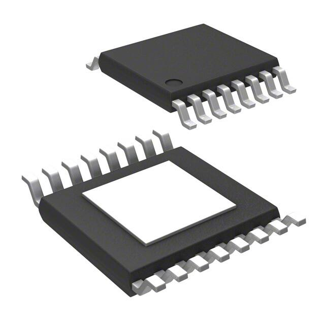


 工商网监
湘ICP备2023018690号
工商网监
湘ICP备2023018690号
