PO
itle
G30
,
301
303
bt
TLmti,
OS
a-
DG300A, DG301A, DG303A
T
CT
DUC
P R O P R OD U
E
T
OL E
UTE
OBS UBSTIT
S
303 Data Sheet
LE
HI-0
SSIB
May 2001
TTL-Compatible, CMOS Analog Switches
Features
The DG300A through DG303A family of monolithic CMOS
switches are truly compatible second source of the original
manufacturer. The switches are latch-proof and are
designed to block signals up to 30V P-P when OFF. Featuring
low leakage and low power consumption, these switches are
ideally suited for precision application in instrumentation,
communication, data acquisition and battery powered
applications. Other key features include Break-Before-Make
switching, TTL and CMOS compatibility, and low ON
resistance. Single supply operation (for positive switch
voltages) is possible by connecting V- to 0V.
• Low Power Consumption
rpoion,
inctor,
itch
OS
PST,
DT,
ST,
DT,
eo,
ET,
alog
3119.3
• Break-Before-Make Switching
- tON . . . . . . . . . . . . . . . . . . . . . . . . . . . . . . . . . . . . 150ns
- tOFF . . . . . . . . . . . . . . . . . . . . . . . . . . . . . . . . . . . 130ns
• TTL, CMOS Compatible
• Low rDS(ON) (Max). . . . . . . . . . . . . . . . . . . . . . . . . . . 50Ω
• Single Supply Operation
• True Second Source
Part Number Information
PART NUMBER
itch
utho
)
eyrds
ter-
File Number
TEMP.
RANGE ( oC)
DG300ABK
-25 to 85
DG301ACJ
0 to 70
DG303AAK
PKG.
NO.
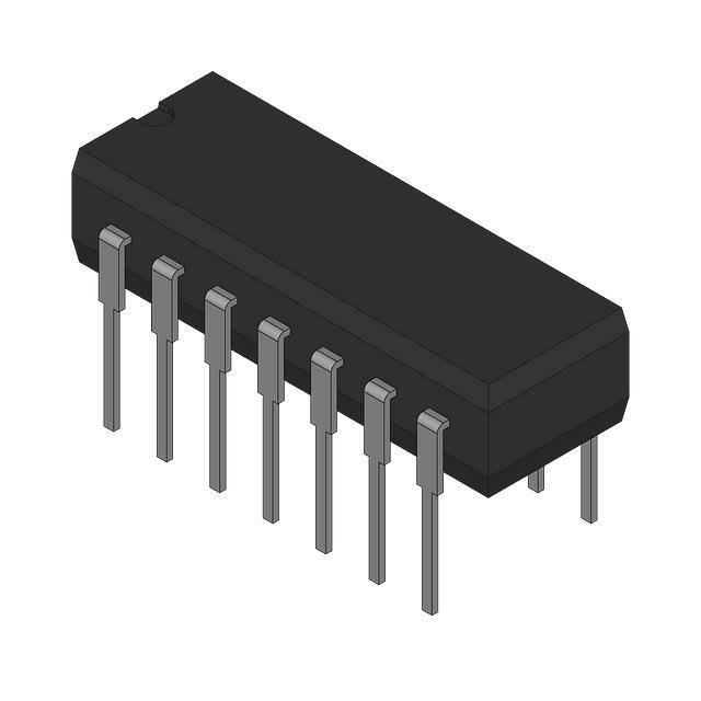
PACKAGE
14 Ld CERDIP
F14.3
14 Ld PDIP
E14.3
-55 to 125
14 Ld CERDIP
F14.3
DG303ABK
-25 to 85
14 Ld CERDIP
F14.3
DG303ACJ
0 to 70
14 Ld PDIP
E14.3
DG303ACY
0 to 70
16 Ld SOIC
M16.3
Functional Diagrams and Pinouts (Switches shown for a logic “1” input)
DG300A
(SPST)
DG300A TRUTH TABLE
S1
LOGIC
SWITCH
0
OFF
NC 1
14 V+
1
ON
D1 2
13 D2
NC 3
12 NC
S1 4
11 S2
NC 5
10 NC
IN 1 6
9 IN2
D1
Logic “0” ≤ 0.8V, Logic “1” ≥ 4.0V.
IN1
IN2
S2
DG300A (CERDIP)
TOP VIEW
D2
GND 7
DG301A
(SPDT)
DG301A (PDIP)
TOP VIEW
DG301A TRUTH TABLE
S1
D1
LOGIC
SWITCH 1
SWITCH 2
0
OFF
ON
NC 1
14 V+
1
ON
OFF
D1 2
13 D2
NC 3
12 NC
Logic “0” ≤ 0.8V, Logic “1” ≥ 4.0V.
S2
D2
IN
S1 4
11 S2
NC 5
10 NC
IN 6
9 NC
GND 7
1
8 V-
8 V-
CAUTION: These devices are sensitive to electrostatic discharge; follow proper IC Handling Procedures.
1-888-INTERSIL or 321-724-7143 | Intersil and Design is a trademark of Intersil Americas Inc. | Copyright © Intersil Americas Inc. 2001
�DG300A, DG301A, DG303A
Functional Diagrams and Pinouts (Switches shown for a logic “1” input)
DG303A
(SPDT)
(Continued)
DG303A (CERDIP, PDIP)
TOP VIEW
NC 1
S1
D1
S3
D3
IN1
D2
S4
D4
14 V+
NC
1
16 V+
15 S4
S3 2
13 S4
S3 2
D3 3
12 D4
D3 3
14 D4
D1 4
13 D2
S1 5
12 S2
IN 1 6
11 IN2
D1 4
11 D2
S1 5
10 S2
IN1 6
9 IN2
IN2
S2
DG303ACY (SOIC)
TOP VIEW
10 V-
GND 7
8 V-
GND 7
NC
8
9 NC
DG303A TRUTH TABLE
LOGIC
SWITCH 1 AND 2
SWITCH 3 AND 4
0
OFF
ON
1
ON
OFF
Logic “0” ≤ 0.8V, Logic “1” ≥ 4.0V.
Pin Descriptions
PIN
SYMBOL
DESCRIPTION
DG300A
PIN
SYMBOL
DESCRIPTION
8
NC
No Connection
9
NC
No Connection
1
NC
No Connection
2
D1
Drain (Output) Terminal for Switch 1
10
S2
Source (Input) Terminal for Switch 2
NC
No Connection
3
NC
No Connection
11
4
S1
Source (Input) Terminal for Switch 1
12
D2
Drain (Output) Terminal for Switch 2
5
NC
No Connection
13
NC
No Connection
6
IN1
Logic Control for Switch 1
14
V+
Positive Power Supply Terminal
Ground Terminal (Logic Common)
DG303A
7
GND
8
V-
Negative Power Supply Terminal
1
NC
No Connection
9
IN2
Logic Control for Switch 2
2
S3
Source (Input) Terminal for Switch 3
10
NC
No Connection
3
D3
Drain (Output) Terminal for Switch 3
D1
Drain (Output) Terminal for Switch 1
11
NC
No Connection
4
12
S2
Source (Input) Terminal for Switch 2
5
S1
Source (Input) Terminal for Switch 1
13
D2
Drain (Output) Terminal for Switch 2
6
IN1
Logic Control for Switch 1
14
V+
Positive Power Supply Terminal
7
GND
8
V-
Negative Power Supply Terminal
9
IN2
Logic Control for Switch 2
S2
Source (Input) Terminal for Switch 2
DG301A
Ground Terminal (Logic Common)
1
NC
No Connection
2
D1
Drain (Output) Terminal for Switch 1
10
3
NC
No Connection
11
D2
Drain (Output) Terminal for Switch 2
D4
Drain (Output) Terminal for Switch 4
4
S1
Source (Input) Terminal for Switch 1
12
5
IN
Logic Control for Switches
13
S4
Source (Input) Terminal for Switch 4
6
GND
Ground Terminal (Logic Common)
14
V+
Positive Power Supply Terminal
7
V-
Negative Power Supply Terminal
2
�DG300A, DG301A, DG303A
Absolute Maximum Ratings
Thermal Information
V+ to V- . . . . . . . . . . . . . . . . . . . . . . . . . . . . . . . . . . . . . . . . . . 44.0V
V- to GND. . . . . . . . . . . . . . . . . . . . . . . . . . . . . . . . . . . . . . . . . . 25V
Digital Inputs, VS, VD (Note 1). . . . . . . . . . . . . (V-) - 2V to (V+) + 2V
or 30mA, Whichever Occurs First
Continuous Current, (Any Terminal). . . . . . . . . . . . . . . . . . . . . 30mA
Peak Current, S or D (Pulsed 1ms, 10% Duty Cycle Max) . . 100mA
Thermal Resistance (Typical, Note 2)
θJA ( oC/W)
θJC (oC/W)
SOIC Package . . . . . . . . . . . . . . . . . . .
100
N/A
PDIP Package . . . . . . . . . . . . . . . . . . .
100
N/A
CERDIP Package. . . . . . . . . . . . . . . . .
75
20
Maximum Junction Temperature
Hermetic Packages . . . . . . . . . . . . . . . . . . . . . . . . . . . . . . 175oC
Plastic Packages . . . . . . . . . . . . . . . . . . . . . . . . . . . . . . . . 150oC
Maximum Storage Temperature Range . . . . . . . . . . -65oC to 150oC
Maximum Lead Temperature (Soldering, 10s). . . . . . . . . . . . 300oC
(SOIC - Lead Tips Only)
Operating Conditions
Voltage Range . . . . . . . . . . . . . . . . . . . . . . . . . . . . . . . . . . . . . ±15V
Temperature Range
“A” Suffix. . . . . . . . . . . . . . . . . . . . . . . . . . . . . . . . -55oC to 125oC
“B” Suffix. . . . . . . . . . . . . . . . . . . . . . . . . . . . . . . . . -25oC to 85oC
“C” Suffix . . . . . . . . . . . . . . . . . . . . . . . . . . . . . . . . . 0oC to 70oC
Input Low Voltage . . . . . . . . . . . . . . . . . . . . . . . . . . . . . 0.8V (Max)
Input High Voltage . . . . . . . . . . . . . . . . . . . . . . . . . . . . . . 4.0V (Min)
Input Rise and Fall Time . . . . . . . . . . . . . . . . . . . . . . . . . . . . ≤20ns
CAUTION: Stresses above those listed in “Absolute Maximum Ratings” may cause permanent damage to the device. This is a stress only rating and operation of the
device at these or any other conditions above those indicated in the operational sections of this specification is not implied.
NOTES:
1. Signals on SX , D X or INX exceeding V+ or V- will be clamped by internal diodes. Limit diode forward current to maximum current ratings.
2. θJA is measured with the component mounted on an evaluation PC board in free air.
V+ = +15V, V- = -15V, GND = 0V, TA = 25oC
Electrical Specifications
“A” SUFFIX
PARAMETER
TEST CONDITIONS
“B” AND “C” SUFFIX
MIN
(NOTE 3)
TYP
MAX
MIN
(NOTE 3)
TYP
MAX
UNITS
DYNAMIC CHARACTERISTICS
Turn-ON Time, tON
See Figure 3
-
150
300
-
150
-
ns
Turn-OFF Time, tOFF
See Figure 3
-
130
250
-
130
-
ns
Break-Before-Make
Interval, tD
See Figure 2, DG301A/DG303A
-
50
-
-
50
-
ns
Charge Injection, Q
CL = 10nF, RS = 0, VS = 0
-
3
-
-
3
-
mV
OFF Isolation (Note 4)
VIN = 0, RL = 1kΩ, VS = 1VRMS ,
f = 500kHz
-
62
-
-
62
-
dB
-
-74
-
-
-74
-
dB
VS = 0
-
14
-
-
14
-
pF
VD = 0
-
14
-
-
14
-
pF
VS = VD = 0
-
40
-
-
40
-
pF
VIN = 0
-
6
-
-
6
-
pF
VIN = 15V
-
7
-
-
7
-
pF
VIN = 5.0V
-1
-0.001
-
-1
-0.001
-
µA
VIN = 15.0V
-
0.001
1
-
0.001
1
µA
VIN = 0V
-1
-0.001
-
-1
-0.001
-
µA
Crosstalk
(Channel-to-Channel)
Source OFF Capacitance,
C S(OFF)
Drain OFF Capacitance,
C D(OFF)
f = 1MHz,
VIN = 0.8V or
VIN = 4.0V
Channel ON Capacitance,
C D(ON) + CS(ON)
Input Capacitance, C IN
f = 1MHz
DIGITAL INPUT CHARACTERISTICS
Input Current with Voltage
High, IIH
Input Current with Voltage
Low, IIL
3
�DG300A, DG301A, DG303A
V+ = +15V, V- = -15V, GND = 0V, TA = 25oC (Continued)
Electrical Specifications
“A” SUFFIX
PARAMETER
“B” AND “C” SUFFIX
MIN
(NOTE 3)
TYP
MAX
MIN
(NOTE 3)
TYP
MAX
UNITS
-15
-
15
-15
-
15
V
IS = -10mA,
VD = 10V
-
30
50
-
30
50
Ω
IS = 10mA,
VD = -10V
-
30
50
-
30
50
Ω
VS = 14V,
VD = -14V
-
0.1
1
-
0.1
5
nA
VS = -14V,
VD = 14V
-1
-0.1
-
-5
-0.1
-
nA
VS = -14V,
VD = 14V
-
0.1
1
-
0.1
5
nA
VS = 14V,
VD = -14V
-1
-0.1
-
-5
-0.1
-
nA
VD = VS = 14V
-
0.1
1
-
0.1
5
nA
VD = VS = -14V
-2
-0.1
-
-5
-0.1
-
nA
-
0.23
0.5
-
0.23
0.5
mA
-10
-0.001
-
-10
-0.001
-
µA
-
0.001
10
-
0.001
10
µA
-10
-0.001
-
-10
-0.001
-
µA
TEST CONDITIONS
ANALOG SWITCH CHARACTERISTICS
Analog Signal Range,
VANALOG
IS = 10mA, VIN = 0.8V or 4V
Drain-Source ON
Resistance, rDS(ON)
VIN = 0.8V or
VIN = 4.0V
Source OFF Leakage
Current, IS(OFF)
Drain OFF Leakage
Current, ID(OFF)
Channel ON Leakage
Current, ID(ON)
VIN = 0.8V or
VIN = 4.0V
VIN = 0.8V or
VIN = 4.0V
VIN = 0.8V or
VIN = 4.0V
POWER SUPPLY CHARACTERISTICS
Positive Supply Current, I+
Negative Supply Current, IPositive Supply Current, I+
VIN = 4V (One Input)
(All Others = 0)
VIN = 0.8V (All Inputs)
Negative Supply Current, I-
Electrical Specifications
V+ = +15V, V- = -15V, GND = 0V, TA = Full Temperature Range
“A” SUFFIX
“B” AND “C” SUFFIX
MIN
(NOTE 3)
TYP
MAX
MIN
(NOTE 3)
TYP
MAX
UNITS
VIN = 5.0V
-1
-
-
-
-
-
µA
VIN = 15.0V
-
-
1
-
-
-
µA
VIN = 0V
-1
-
-
-
-
-
µA
-15
-
15
-
-
-
V
IS = -10mA,
VD = 10V
-
-
75
-
-
-
Ω
IS = 10mA,
VD = -10V
-
-
75
-
-
-
Ω
VS = 14V,
VD = -14V
-
-
100
-
-
-
nA
VS = -14V,
VD = 14V
-100
-
-
-
-
-
nA
PARAMETER
TEST CONDITION
DIGITAL INPUT CHARACTERISTICS
Input Current with Voltage
High, IIH
Input Current with Voltage
Low, IIL
ANALOG SWITCH CHARACTERISTICS
Analog Signal Range,
VANALOG
IS = 10mA, VIN = 0.8V or 4V
Drain-Source ON
Resistance, rDS(ON)
VIN = 0.8V or
VIN = 4.0V
Source OFF Leakage
Current, IS(OFF)
VIN = 0.8V or
VIN = 4.0V
4
�DG300A, DG301A, DG303A
Electrical Specifications
V+ = +15V, V- = -15V, GND = 0V, TA = Full Temperature Range (Continued)
“A” SUFFIX
PARAMETER
MIN
(NOTE 3)
TYP
MAX
MIN
(NOTE 3)
TYP
MAX
UNITS
VS = -14V,
VD = 14V
-
-
100
-
-
-
nA
VS = 14V,
VD = -14V
-100
-
-
-
-
VD = VS = 14V
-
-
100
-
-
-
nA
VD = VS = -14V
-200
-
-
-
-
-
nA
-
-
1
-
-
-
mA
-100
-
-
-
-
-
µA
-
-
100
-
-
-
µA
-100
-
-
-
-
-
µA
TEST CONDITION
Drain OFF Leakage
Current, ID(OFF)
VIN = 0.8V or
VIN = 4.0V
Channel ON Leakage
Current, ID(ON)
VIN = 0.8V or
VIN = 4.0V
“B” AND “C” SUFFIX
nA
POWER SUPPLY CHARACTERISTICS
Positive Supply Current, I+
Negative Supply Current, IPositive Supply Current, I+
VIN = 4V (One Input)
(All Others = 0)
VIN = 0.8V (All Inputs)
Negative Supply Current, INOTES:
3. For design only, not 100% tested.
4. OFF isolation = 20 Log VS /V D, where VS = input to OFF switch, and VD = output.
Test Circuits and Waveforms
∆VO
RS
SX
DX
VD
VD
INX
VS
CL = 10nF
INX
ON
ON
OFF
FIGURE 1. CHARGE INJECTION TEST CIRCUIT AND MEASUREMENT POINTS
LOGIC “1” = SWITCH ON
5V
LOGIC
INPUT
V+ 15V
VS1 = 3V
S1
D1
VS2 = 3V
S2
D2
LOGIC
INPUT
GND
V-15V
VS1
SWITCH
OUTPUT
VO1
RL2
300
Ω
IN
RL1
300
Ω
CL2
VO2
CL1
33pF
33pF
0V
SWITCH
OUTPUT
(VO1)
50%
0V
tD
VS2
SWITCH
OUTPUT
(VO2)
0V
50%
0V
FIGURE 2. BREAK-BEFORE MAKE TEST CIRCUIT AND MEASUREMENT POINTS (DG301A, DG303A)
5
�DG300A, DG301A, DG303A
Test Circuits and Waveforms
(Continued)
LOGIC “1” = SWITCH ON
V+ +15V
VS = 3V
S
SWITCH
OUTPUT
VO
D
LOGIC
INPUT
SWITCH
INPUT
LOGIC
INPUT
IN
RL
300
kΩ
GND
V-15V
tr < 20ns
tf < 20ns
5V
50%
0V
VS
CL
33pF
90%
SWITCH
OUTPUT
10%
0V
tON
FIGURE 3. t ON and tOFF TEST CIRCUIT AND MEASUREMENT POINTS
Die Characteristics
DIE DIMENSIONS:
89 mils x 99 mils x 12 mils
METALLIZATION:
Type: Al
Thickness: 10kÅ ±1kÅ
PASSIVATION:
Type: PSG Over Nitride
PSG Thickness: 7kÅ ±1.4kÅ
Nitride Thickness: 8kÅ ±1.2kÅ
WORST CASE CURRENT DENSITY:
1 x 10⁵ A/cm2
6
tOFF
�DG300A, DG301A, DG303A
Metallization Mask Layouts
DG300A
DG301A
PIN 14
V+
PIN 14
V+
PIN 2
D1
PIN 13
D2
PIN 2
D1
PIN 13
D2
PIN 4
S1
PIN 11
S2
PIN 4
S1
PIN 11
S2
PIN 6
IN 1
NC
PIN 7
GND
PIN 6
IN 1
PIN 9
IN 2
PIN 8
V-
NC
PIN 7
GND
PIN 8
V-
DG303A
PIN 14
V+
PIN 2
S3
PIN 13
S4
PIN 3
D3
PIN 4
D1
PIN 12
D4
PIN 11
D2
PIN 5
S1
PIN 10
S2
PIN 6
IN 1
NC
PIN 7
GND
PIN 8
V-
PIN 9
IN 2
All Intersil products are manufactured, assembled and tested utilizing ISO9000 quality systems.
Intersil Corporation’s quality certifications can be viewed at website www.intersil.com/design/quality/iso.asp
Intersil products are sold by description only. Intersil Corporation reserves the right to make changes in circuit design and/or specifications at any time without notice.
Accordingly, the reader is cautioned to verify that data sheets are current before placing orders. Information furnished by Intersil is believed to be accurate and reliable. However, no responsibility is assumed by Intersil or its subsidiaries for its use; nor for any infringements of patents or other rights of third parties which may result from its use.
No license is granted by implication or otherwise under any patent or patent rights of Intersil or its subsidiaries.
For information regarding Intersil Corporation and its products, see web site www.intersil.com
Sales Office Headquarters
EUROPE
Intersil SA
Mercure Center
100, Rue de la Fusee
1130 Brussels, Belgium
TEL: (32) 2.724.2111
FAX: (32) 2.724.22.05
NORTH AMERICA
Intersil Corporation
2401 Palm Bay Rd.
Palm Bay, FL 32905
TEL: (321) 724-7000
FAX: (321) 724-7240
7
ASIA
Intersil Ltd.
8F-2, 96, Sec. 1, Chien-kuo North,
Taipei, Taiwan 104
Republic of China
TEL: 886-2-2515-8508
FAX: 886-2-2515-8369
�


 工商网监
湘ICP备2023018690号
工商网监
湘ICP备2023018690号
