INDUSTRIAL EMBEDDED MULTIMEDIA CARD (EMMC)
401-0410-00 Rev F
G530 Series
Embedded Multimedia Card
e•MMC™ 5.0 HS400
Engineering Specification
Document Number: 401-0410-00
Revision: F
___________________________________________________________________________________________________________________
© 2020 | Delkin Devices Inc.
1
�INDUSTRIAL EMBEDDED MULTIMEDIA CARD (EMMC)
401-0410-00 Rev F
TABLE OF CONTENTS
1. Introduction ............................................................................................................................ 5
2. Specification ........................................................................................................................... 5
2.1. System Performance ............................................................................................................. 5
2.2. Power Consumption .............................................................................................................. 6
2.3. Capacity by Partition ............................................................................................................. 6
2.4. User Density .......................................................................................................................... 6
3. e•MMC™ Device and System ................................................................................................. 7
3.1. e•MMC™ System Overview ................................................................................................... 7
3.2. Memory Addressing .............................................................................................................. 7
3.3. e•MMC™ Device Overview .................................................................................................... 8
3.3.1 Clock (CLK) .................................................................................................................... 8
3.3.2 Data Strobe (DS) ............................................................................................................ 8
3.3.3 Command (CMD) ........................................................................................................... 8
3.3.4 Input/Outputs (DAT0-DAT7) ........................................................................................... 8
3.4. Bus Protocol ........................................................................................................................ 10
3.5. Bus Speed Modes ............................................................................................................... 10
3.5.1 HS200 Bus Speed Mode .............................................................................................. 10
3.5.2 HS200 System Block Diagram ..................................................................................... 11
3.5.3 HS400 Bus Speed mode .............................................................................................. 12
3.5.4 HS400 System Block Diagram ..................................................................................... 12
4. e•MMC™ Functional Description ......................................................................................... 13
4.1 e•MMC™ Overview .............................................................................................................. 13
4.2 Boot Operation Mode .......................................................................................................... 13
4.3 Device Identification Mode .................................................................................................. 13
4.4 Interrupt Mode ..................................................................................................................... 13
4.5 Data Transfer Mode ............................................................................................................ 13
4.6 Inactive Mode ...................................................................................................................... 14
4.7 H/W Reset Operation .......................................................................................................... 14
4.8 Noise Filtering Timing for H/W Reset .................................................................................. 15
4.9 Field Firmware Update(FFU) ............................................................................................... 16
4.10 Power off Notification for sleep ............................................................................................ 17
5. Register Settings .................................................................................................................. 19
5.1. OCR Register ...................................................................................................................... 19
5.2. CID Register ........................................................................................................................ 19
5.3. CSD Register ...................................................................................................................... 19
5.4. Extended CSD Register ...................................................................................................... 19
5.5. RCA Register ...................................................................................................................... 19
5.6. DSR Register ...................................................................................................................... 19
6. The e•MMC™ bus .................................................................................................................. 20
6.1 Power-up ............................................................................................................................. 21
6.1.1 e•MMC™ power-up ....................................................................................................... 21
6.1.2 e•MMC™ Power Cycling ............................................................................................... 22
6.2 Bus Operating Conditions.................................................................................................... 23
6.2.1 Power supply: e•MMC™................................................................................................ 23
___________________________________________________________________________________________________________________
© 2020 | Delkin Devices Inc.
2
�INDUSTRIAL EMBEDDED MULTIMEDIA CARD (EMMC)
401-0410-00 Rev F
6.2.2 e•MMC™ Power Supply Voltage ................................................................................... 24
6.2.3 Bus Signal Line Load ................................................................................................... 25
6.2.4 HS400 reference load .................................................................................................. 26
6.3 Bus Signal Levels ................................................................................................................ 27
6.3.1 Open-drain Mode Bus Signal Level .............................................................................. 27
6.3.2 Push-pull mode bus signal level— e•MMC™ ................................................................ 27
6.3.3 Bus Operating Conditions for HS200 & HS400 ............................................................ 28
6.3.4 Device Output Driver Requirements for HS200 & HS400 ............................................ 28
6.4 Bus Timing .......................................................................................................................... 28
6.4.1 Device Interface Timing................................................................................................ 29
6.5 Bus Timing for DAT Signals During Dual Data Rate Operation ........................................... 30
6.6 Bus Timing Specification in HS200 Mode............................................................................ 31
6.7 Bus Timing Specification in HS400 mode............................................................................ 35
6.7.1 HS400 Device Input Timing.......................................................................................... 35
6.7.2 HS400 Device Output Timing ....................................................................................... 36
7. Package Connections .......................................................................................................... 38
7.1. Package Mechanical .......................................................................................................... 38
7.1.1. 11.5 x 13.0 x 1mm 153 Ball Package ........................................................................... 38
8. Ball Assignments ................................................................................................................. 40
8.1. 153 Ball Package ............................................................................................................... 40
9. Temperature.......................................................................................................................... 41
10. Ordering Information ........................................................................................................... 41
___________________________________________________________________________________________________________________
© 2020 | Delkin Devices Inc.
3
�INDUSTRIAL EMBEDDED MULTIMEDIA CARD (EMMC)
401-0410-00 Rev F
Product Features:
•
•
•
•
•
•
•
•
•
•
•
•
•
•
•
Packaged NAND flash memory with e•MMC™ 5.0 interface
Compliant with e•MMC™ Specification Ver.4.4, 4.41,4.5 and 5.0
Bus mode
High-speed e•MMC™ protocol
Clock frequency: 0-200MHz.
Ten-wire bus (clock, 1 bit command, 8 bit data bus) and a hardware reset.
Supports three different data bus widths : 1 bit(default), 4 bits, 8 bits
Data transfer rate: up to 52Mbyte/s (using 8 parallel data lines at 52 MHz)
Single data rate : up to 200Mbyte/s @ 200MHz
Dual data rate : up to 400Mbytes/s @200MHz
Operating voltage range :
VCCQ = 1.8 V/3.3 V
VCC = 3.3 V
Error free memory access
Internal error correction code (ECC) to protect data communication
Internal enhanced data management algorithm
Solid protection of sudden power failure safe-update operations for data content
Security
Supports secure bad block erase commands
Enhanced Write Protection with permanent and partial protection options
Quality
RoHS compliant (for detailed RoHS declaration, please contact your Delkin representative.)
Supports Field Firmware Update (FFU)
Enhanced Device Life Time
Supports pre EOL information
Supports Production State Awareness
Supports Power Off Notification for Sleep
Supports HS400
Temperature Range:
Operating: -40 to +85°C
Storage: -40 to +85°C
___________________________________________________________________________________________________________________
© 2020 | Delkin Devices Inc.
4
�INDUSTRIAL EMBEDDED MULTIMEDIA CARD (EMMC)
401-0410-00 Rev F
1. Introduction
Delkin Devices e•MMC™ products comply with the JEDEC e•MMC™ 5.0 standard and are an ideal
universal storage solution for many embedded devices. E•MMC™ combines MLC NAND and an
e•MMC™ controller inside one JEDEC standard package, providing a standard interface to the host.
Delkin offers the 153 ball (11.5 x 13 x 1.0mm package), in MLC and pSLC configurations. The e•MMC™
controller directly manages NAND flash, including ECC, wear-leveling, IOPS optimization and read
sensing.
Table 1 – Device Summary
Flash Configuration Available Capacities
Package
FBGA153
MLC
4GB – 8GB
11.5 x 13 x 1.0mm
pSLC
FBGA153
2GB – 4GB
(single user partition)
11.5 x 13 x 1.0mm
Refer to part number table in Section 10.
Operating Voltage
VCC=3.3V,
VCCQ=1.8V/3.3V
2. Specification
2.1. System Performance
Product Configuration
4GB MLC
Table 2- Read/Write Performance
Typical Value
Read Sequential
Write Sequential
(MB/s)
(MB/s)
14
8GB MLC
25
250
2GB pSLC
30
4GB pSLC
80
Note 1: Values given for an 8-bit bus width, running HS400 mode from proprietary tool, VCC=3.3V,VCCQ=1.8V.
Note 2: For performance numbers under other test conditions, please contact Delkin.
Note 3: Performance numbers might be subject to change without notice.
___________________________________________________________________________________________________________________
© 2020 | Delkin Devices Inc.
5
�INDUSTRIAL EMBEDDED MULTIMEDIA CARD (EMMC)
401-0410-00 Rev F
2.2. Power Consumption
Products
4GB MLC or 2GB pSLC
Table 3–Device Power Consumption
Read (mA)
Write mA)
VCCQ (1.8V)
Vcc(3.3V)
VCCQ (1.8V)
Vcc(3.3V)
100
80
50
30
8GB MLC or 4GB pSLC
160
50
100
40
Standby (mA)
Typ
0.12
0.16
Note 1; Values given for an 8-bit bus width, a clock frequency of 200MHz DDR mode, VCC= 3.3V±5%, VCCQ=1.8V±5%.
Note 2: Standby current is measured at Vcc = 3.3V ±5%, 8-bit bus width without clock frequency
Note 2: Current numbers might be subject to change without notice.
2.3. Capacity by Partition
Device
Boot Partition 1
4GB MLC or 2GB pSLC
8GB MLC or 4GB pSLC
2048 KB
4096 KB
Boot Partition 2
2048 KB
4096 KB
RPMB
512KB
4096 KB
2.4. User Density
Device
4GB MLC
User Density
3,901,415,424 Bytes
8GB MLC
7,802,871,808 Bytes
2GB pSLC
4GB pSLC
1,954,217,984 Bytes
3,901,415,424 Bytes
___________________________________________________________________________________________________________________
© 2020 | Delkin Devices Inc.
6
�INDUSTRIAL EMBEDDED MULTIMEDIA CARD (EMMC)
401-0410-00 Rev F
3. e•MMC™ Device and System
3.1. e•MMC™ System Overview
The e•MMC™ specification covers the behavior of the interface and the Device controller. As part
of this specification, the existence of a host controller and a memory storage array are implied but
the operation of these pieces is not fully specified.
Delkin’s NAND device consists of a single chip MMC controller and NAND flash memory module.
The micro-controller interfaces with a host system allowing data to be written to and read from the
NAND flash memory module. The controller allows the host to be independent from details of
erasing and programming the flash memory.
Figure 1– e•MMC™ System Overview
3.2. Memory Addressing
Previous implementations of the e•MMC™ specification follow byte addressing with 32 bit field. This
addressing mechanism is permitted for e•MMC™ densities up to and including 2 GB.
To support larger densities the addressing mechanism was updated to support sector addresses
(512 B sectors). The sector addresses shall be used for all devices with capacity larger than 2 GB.
To determine the addressing mode use the host should read bit [30:29] in the OCR register.
___________________________________________________________________________________________________________________
© 2020 | Delkin Devices Inc.
7
�INDUSTRIAL EMBEDDED MULTIMEDIA CARD (EMMC)
401-0410-00 Rev F
3.3. e•MMC™ Device Overview
The e•MMC™ device transfers data via a configurable number of data bus signals. The
communication signals are:
3.3.1 Clock (CLK)
Each cycle of this signal directs a one bit transfer on the command and either a one bit (1x) or
two bit transfer (2x) on all the data lines. The frequency may vary between zero and the
maximum clock frequency.
3.3.2 Data Strobe (DS)
This signal is generated by the device and used for output in HS400 mode. The frequency of
this signal follows the frequency of CLK. For data output each cycle of this signal directs two
bits transfer (2x) on the data - one bit for positive edge and the other bit for negative edge. For
CRC status response output and CMD response output (enabled only HS400 enhanced strobe
mode), the CRC status is latched on the positive edge only, and ignores the negative edge.
3.3.3 Command (CMD)
This signal is a bidirectional command channel used for Device initialization and transfer of
commands. The CMD signal has two operation modes: open-drain for initialization mode, and
push-pull for fast command transfer. Commands are sent from the e•MMC™ host controller to
the e•MMC™ Device and responses are sent from the Device to the host.
3.3.4 Input/Outputs (DAT0-DAT7)
These are bidirectional data channels. The DAT signals operate in push-pull mode. Either the
Device or the host is driving these signals at any given time. By default, after power up or reset,
only DAT0 is used for data transfer. A wider data bus can be configured for data transfer, using
either DAT0-DAT3 or DAT0-DAT7, by the e•MMC™ host controller. The e•MMC™ Device
includes internal pull-ups for data lines DAT1-DAT7. Immediately after entering 4-bit mode, the
Device disconnects the internal pull ups of lines DAT1, DAT2, and DAT3. Correspondingly,
immediately after entering 8-bit mode, the Device disconnects the internal pull-ups of lines
DAT1–DAT7.
___________________________________________________________________________________________________________________
© 2020 | Delkin Devices Inc.
8
�INDUSTRIAL EMBEDDED MULTIMEDIA CARD (EMMC)
401-0410-00 Rev F
Table 4– Communication Interface
Type1
I
I/O/PP
Name
CLK
DAT0
DAT1
DAT2
DAT3
DAT4
DAT5
DAT6
DAT7
CMD
RST_n
VCC
VCCQ
VSS
VSSQ
DS
Description
Clock
Data
Data
Data
Data
Data
Data
Data
Data
Command/Response
Hardware reset
Supply voltage for Core
Supply voltage for I/O
Supply voltage ground for Core
Supply voltage ground for I/O
Data strobe
I/O/PP
I/O/PP
I/O/PP
I/O/PP
I/O/PP
I/O/PP
I/O/PP
I/O/PP/OD
I
S
S
S
S
O/PP
Note1:I: input; O: output; PP: push-pull; OD: open-drain; NC: Not connected (or logical high); S: power supply.
Table 5– e•MMC™ Registers
Name
Width
(Bytes)
CID
16
RCA
2
DSR
2
CSD
16
OCR
4
EXT_CSD
512
Description
Device Identification number, an individual number for
identification.
Relative Device Address is the Device system address,
dynamically assigned by the host during initialization.
Driver Stage Register, to configure the Device’s output drivers.
Device Specific Data, information about the Device operation
conditions.
Operation Conditions Register. Used by a special broadcast
command to identify the voltage type of the Device.
Extended Device Specific Data. Contains information about the
Device capabilities and selected modes. Introduced in standard
v4.0
Implementation
Mandatory
Mandatory
Optional
Mandatory
Mandatory
Mandatory
The host may reset the device by:
•
•
•
Switching the power supply off and back on. The device shall have its own power-on detection
circuitry which puts the device into a defined state after the power-on Device.
A reset signal
By sending a special command
___________________________________________________________________________________________________________________
© 2020 | Delkin Devices Inc.
9
�INDUSTRIAL EMBEDDED MULTIMEDIA CARD (EMMC)
401-0410-00 Rev F
3.4. Bus Protocol
After a power-on reset, the host must initialize the device by a special message-based e•MMC™
bus protocol. For more details, refer to section 5.3.1 of the JEDEC Standard Specification
No.JESD84-B51.
3.5. Bus Speed Modes
e•MMC™ defines several bus speed modes as shown in Table 6.
Table 6— Bus Speed Mode
Data Rate
IO Voltage
Bus Width
Frequency
Max Data Transfer
(implies x8 bus width)
Single
3.3/1.8V
1, 4, 8
0-26MHz
26MB/s
Single
3.3/1.8V
4, 8
0-52MHz
52MB/s
Dual
3.3/1.8V
4, 8
0-52MHz
104MB/s
HS200
Single
1.8V
4, 8
0-200MHz
200MB/s
HS400
Dual
1.8V
8
0-200MHz
400MB/s
Mode Name
Backwards
Compatibility with
legacy MMC card
High Speed SDR
High Speed DDR
3.5.1 HS200 Bus Speed Mode
The HS200 mode offers the following features:
•
•
•
•
•
•
SDR Data sampling method
CLK frequency up to 200MHz Data rate – up to 200MB/s
8-bits bus width supported
Single ended signaling with 4 selectable Drive Strength
Signaling levels of 1.8V
Tuning concept for Read Operations
___________________________________________________________________________________________________________________
© 2020 | Delkin Devices Inc.
10
�INDUSTRIAL EMBEDDED MULTIMEDIA CARD (EMMC)
401-0410-00 Rev F
3.5.2 HS200 System Block Diagram
Figure 2 shows a typical HS200 Host and Device system. The host has a clock generator,
which supplies CLK to the Device. For write operations, clock and data direction are the
same, write data can be transferred synchronous with CLK, regardless of transmission line
delay. For read operations, clock and data direction are opposite; the read data received by
Host is delayed by round-trip delay, output delay and latency of Host and Device. For reads,
the Host needs to have an adjustable sampling point to reliably receive the incoming data
Figure 2— System Block Diagram
___________________________________________________________________________________________________________________
© 2020 | Delkin Devices Inc.
11
�INDUSTRIAL EMBEDDED MULTIMEDIA CARD (EMMC)
401-0410-00 Rev F
3.5.3 HS400 Bus Speed mode
The HS400 mode has the following features
•
DDR Data sampling method
•
CLK frequency up to 200MHz, Data rate is – up to 400MB/s
•
Only 8-bit bus width supported
•
Signaling levels of 1.8V
•
Support up to 5 selective Drive Strength
• Data strobe signal is toggled only for Data out and CRC response
3.5.4 HS400 System Block Diagram
Figure 3 shows a typical HS400 Host and Device system. The host has a clock generator, which
supplies CLK to the Device. For read operations, Data Strobe is generated by device output
circuit. Host receives the data which is aligned to the edge of Data Strobe.
Figure 3- HS400 Host and Device block diagram
___________________________________________________________________________________________________________________
© 2020 | Delkin Devices Inc.
12
�INDUSTRIAL EMBEDDED MULTIMEDIA CARD (EMMC)
401-0410-00 Rev F
4. e•MMC™ Functional Description
4.1 e•MMC™ Overview
All communication between the host and device are controlled by the host (main chip). The host
sends a command, which results in a device response. For more details, refer to section 6.1 of
the JEDEC Standard Specification No.JESD84-B50.
Five operation modes are defined for the e•MMC™ system:
•
•
•
•
•
Boot operation mode
Device identification mode
Interrupt mode
Data transfer mode
Inactive mode
4.2 Boot Operation Mode
In boot operation mode, the master (e•MMC™ host) can read boot data from the slave (e•MMC™
device) by keeping CMD line low or sending CMD0 with argument + 0xFFFFFFFA, before issuing
CMD1. The data can be read from either boot area or user area depending on register setting. For
more details, refer to section 6.3 of the JEDEC Standard Specification No.JESD84-B50.
4.3 Device Identification Mode
While in device identification mode the host resets the device, validates operation voltage range
and access mode, identifies the device and assigns a Relative device Address (RCA) to the device
on the bus. All data communication in the Device Identification Mode uses the command line (CMD)
only. For more details, refer to section 6.4 of the JEDEC Standard Specification No.JESD84-B50.
4.4 Interrupt Mode
The interrupt mode on the e•MMC™ system enables the master (e•MMC™ host) to grant the
transmission allowance to the slaves (Device) simultaneously. This mode reduces the polling load
for the host and hence, the power consumption of the system, while maintaining adequate
responsiveness of the host to a Device request for service. Supporting e•MMC™ interrupt mode is
an option, both for the host and the Device. For more details, refer to section 6.5 of the JEDEC
Standard Specification No.JESD84-B50.
4.5 Data Transfer Mode
When the Device is in Stand-by State, communication over the CMD and DAT lines will be
performed in push-pull mode. For more details, refer to section 6.6 of the JEDEC Standard
Specification No.JESD84-B50.
___________________________________________________________________________________________________________________
© 2020 | Delkin Devices Inc.
13
�INDUSTRIAL EMBEDDED MULTIMEDIA CARD (EMMC)
401-0410-00 Rev F
4.6 Inactive Mode
The device will enter inactive mode if either the device operating voltage range or access mode is
not valid. The device can also enter inactive mode with GO_INACTIVE_STATE command
(CMD15). The device will reset to Pre-idle state with power cycle. For more details, refer to section
6.1 of the JEDEC Standard Specification No.JESD84-B50.
4.7
H/W Reset Operation
Figure 4– H/W Reset Waveform
Note1: Device will detect the rising edge of RST_n signal to trigger internal reset sequence
Table 7– H/W Reset Timing Parameters
Symbol
Comment
tRSTW
RST_n pulse width
tRSCA
RST_n to Command time
tRSTH
RST_n high period (interval time)
Min
Max
Unit
1
[us]
2001
[us]
1
[us]
Note1:74 cycles of clock signal required before issuing CMD1 or CMD0 with argument 0xFFFFFFFA
___________________________________________________________________________________________________________________
© 2020 | Delkin Devices Inc.
14
�INDUSTRIAL EMBEDDED MULTIMEDIA CARD (EMMC)
4.8
401-0410-00 Rev F
Noise Filtering Timing for H/W Reset
Device must filter out 5ns or less pulse width for noise immunity
Figure 5– Noise Filtering Timing for H/W Reset
Device must not detect the rising edge.
Device must not detect 5ns or less of positive or negative RST_n pulse.
Device must detect more than or equal to 1us of positive or negative RST_n pulse width.
___________________________________________________________________________________________________________________
© 2020 | Delkin Devices Inc.
15
�INDUSTRIAL EMBEDDED MULTIMEDIA CARD (EMMC)
4.9
401-0410-00 Rev F
Field Firmware Update(FFU)
Field Firmware Updates (FFU) enables features enhancement in the field. Using this
mechanism the host downloads a new version of the firmware to the e.MMC device and, following
a successful download, instructs the e.MMC device to install the new downloaded firmware into
the device.
In order to start the FFU process the host first checks if the e.MMC device supports FFU
capabilities by reading SUPPPORTED_MODES and FW_CONFIG fields in the EXT_CSD. If the
e.MMC device supports the FFU feature the host may start the FFU process. The FFU process
starts by switching to FFU Mode in MODE_CONFIG field in the EXT_CSD. In FFU Mode host
should use closed-ended or open ended commands for downloading the new firmware and
reading vendor proprietary data. In this mode, the host should set the argument of these
commands to be as defined in FFU_ARG field. In case these commands have a different
argument the device behavior is not defined and the FFU process may fail. The host should set
Block Length to be DATA_SECTOR_SIZE. Downloaded firmware bundle must be
DATA_SECTOR_SIZE size aligned (internal padding of the bundle might be required).Once in
FFU Mode the host may send the new firmware bundle to the device using one or more write
commands.
The host could regain regular functionality of write and read commands by setting
MODE_CONFIG field in the EXT_CSD back to Normal state. Switching out of FFU Mode may
abort the firmware download operation. When host switched back to FFU Mode, the host should
check the FFU Status to get indication about the number of sectors which were downloaded
successfully by reading the NUMBER_OF_FW_SECTORS_CORRECTLY_PROGRAMMED in
the extended CSD. In case the number of sectors downloaded successfully is zero, the host
should re-start downloading the new firmware bundle from its first sector. In case the number of
sectors which were downloaded successfully is positive, the host should continue the download
from the next sector, which would resume the firmware download operation.
In case MODE_OPERATION_CODES field is not supported by the device, the host sets to
NORMAL state and initiates a CMD0/HW_Reset/Power cycle to install the new firmware. In such
case the device doesn’t need to use NUMBER_OF_FW_SECTORS_CORRECTLY_PROGRAMMED.
In both cases, occurrence of a CMD0/HW_Reset/Power before the host successfully downloaded
the new firmware bundle to the device may cause the firmware download process to be aborted.
___________________________________________________________________________________________________________________
© 2020 | Delkin Devices Inc.
16
�INDUSTRIAL EMBEDDED MULTIMEDIA CARD (EMMC)
401-0410-00 Rev F
4.10 Power off Notification for sleep
The host should notify the device before it powers the device off – by turning off all of its power
supplies. This allows the device to better prepare itself for power down. In particular, the host
should issue a power off notification (POWER_OFF_LONG, POWER_OFF_SHORT ) if it intends
to turn off both VCC and VCCQ power I or it may use a power off notification
(SLEEP_NOTIFICATION ) if it intends to turn-off VCC after moving the device to Sleep state.
To indicate to the device that power off notification is supported by the host, a supporting host
shall first set the POWER_OFF_NOTIFICATION byte in EXT_CSD [34] to POWERED_ON
(0x01). To execute a power off, before powering the device down, the host will change the value
to either POWER_OFF_SHORT (0x02) or POWER_OFF_LONG (0x03). The host should wait for
the busy line to be de-asserted. Once the setting has changed to either 0x02 or 0x03, host may
safely power off the device.
The host may issue SLEEP_AWAKE (CMD5) to enter or to exit from Sleep state if
POWER_OFF_NOTIFICATION byte is set to POWERED_ON. Before moving to Standby state
and then to Sleep state, the host sets POWER_OFF_NOTIFICATION to SLEEP_NOTIFICATION
and waits for the DAT0 line de-assertion. While in Sleep (slp) state, VCC (Memory supply) may
be turned off as defined in 4.1.6. Removing power supplies other than VCC while the device is in
the Sleep (slp) state may result in undefined device behavior. Before removing all power supplies,
the host should transition the device out of Sleep (slp) state back to Transfer state using CMD5
and CMD7 and then execute a power off notification setting POWER_OFF_NOTIFICATION byte
to either POWER_OFF_SHORT or POWER_OFF_LONG.
If host continues to send commands to the device after switching to the power off setting (PO
WER_OFF_LONG, POWER_OFF_SHORT or SLEEP_NOTIFICATION) or performs HPI during t
he busy condition, the device shall restore the POWER_OFF_NOTIFICATION byte to POWERED
_ON.
If the host tries to change POWER_OFF_NOTIFICATION to 0x00 after writing another value ther
e, a SWITCH_ERROR is generated.
The difference between the two power-off modes is the urgency with which the host wants to
turn power off. The device should respond to POWER_OFF_SHORT quickly under the generic
CMD6 timeout. If more time is acceptable, POWER_OFF_LONG may be used and the device
shall respond to it within the POWER_OFF_LONG_TIME timeout.
While POWER_OFF_NOTIFICATION is set to POWERED_ON, the device expects the host to
host shall:
•Keep the device power supplies alive (both VCC and VCCQ) and in their active mode
•Not power off the device intentionally before changing POWER_OFF_NOTIFICATION to
either POWER_OFF_LONG or POWER_OFF_SHORT
___________________________________________________________________________________________________________________
© 2020 | Delkin Devices Inc.
17
�INDUSTRIAL EMBEDDED MULTIMEDIA CARD (EMMC)
401-0410-00 Rev F
•Not power off VCC intentionally before changing POWER_OFF_NOTIFICATION to
SLEEP_NOTIFICATION and before moving the device to Sleep state
Before moving to Sleep state, hosts may set the POWER_OFF_NOTIFICATION byte to
SLEEP_NOTIFICATION (0x04) if aware that the device is capable of autonomously initiating
background operations for possible performance improvements. Host should wait for the busy
line to be de-asserted. Busy line may be asserted up the period defined in
SLEEP_NOTIFICATION_TIME byte in EXT_CSD [216]. Once the setting has changed to 0x04
host may set the device into Sleep mode (CMD7+CMD5). After exiting from Sleep, the
POWER_OFF_NOTIFICATION byte will restore its value to POWERED_ON. HPI may interrupt
the SLEEP_NOTIFICATION operation. In that case POWER_OFF_NOTIFICATION byte will
restore to POWERED_ON.
___________________________________________________________________________________________________________________
© 2020 | Delkin Devices Inc.
18
�INDUSTRIAL EMBEDDED MULTIMEDIA CARD (EMMC)
401-0410-00 Rev F
5. Register Settings
Within the Device interface six registers are defined: OCR, CID, CSD, EXT_CSD, RCA and
DSR. These can be accessed only by corresponding commands (see Section 6.10 of JESD84B50).
5.1. OCR Register
The 32-bit operation conditions register (OCR) stores the VDD voltage profile of the Device and the
access mode indication. In addition, this register includes a status information bit. This status bit is
set if the Device power up procedure has been finished. The OCR register shall be implemented
by all Devices.
5.2. CID Register
The Card Identification (CID) register is 128 bits wide. It contains the Device identification
information used during the Device identification phase (e•MMC™ protocol). For details, refer to
JEDEC Standard Specification No.JESD84-B50.
5.3. CSD Register
The Card-Specific Data (CSD) register provides information on how to access the contents stored
in e•MMC™. The CSD registers are used to define the error correction type, maximum data access
time, data transfer speed, data format…etc. For details, refer to section 7.3 of the JEDEC Standard
Specification No.JESD84-B50.
5.4. Extended CSD Register
The Extended CSD register defines the Device properties and selected modes. It is 512 bytes long.
The most significant 320 bytes are the Properties segment, which defines the Device capabilities
and cannot be modified by the host. The lower 192 bytes are the Modes segment, which defines
the configuration the Device is working in. These modes can be changed by the host by means of
the SWITCH command. For details, refer to section 7.4 of the JEDEC Standard Specification
No.JESD84-B50.
5.5. RCA Register
The writable 16-bit Relative Device Address (RCA) register carries the Device address assigned
by the host during the Device identification. This address is used for the addressed host-Device
communication after the Device identification procedure. The default value of the RCA register is
0x0001. The value 0x0000 is reserved to set all Devices into the Stand-by State with CMD7. For
detailed register setting value, please refer to appendix or contact Delkin.
5.6. DSR Register
The 16-bit driver stage register (DSR) is described in detail in Section 7.6 of the JEDEC Standard
Specification No.JESD84-B50. It can be optionally used to improve the bus performance for
extended operating conditions (depending on parameters like bus length, transfer rate or number
of Devices). The CSD register carries the information about the DSR register usage. For detailed
register setting value, please refer to appendix or contact Delkin.
___________________________________________________________________________________________________________________
© 2020 | Delkin Devices Inc.
19
�INDUSTRIAL EMBEDDED MULTIMEDIA CARD (EMMC)
401-0410-00 Rev F
6. The e•MMC™ bus
The e•MMC™ bus has ten communication lines and three supply lines:
• CMD: Command is a bidirectional signal. The host and Device drivers are operating in
two modes, open drain and push/pull.
• DAT0-7: Data lines are bidirectional signals. Host and Device drivers are operating in
push-pull mode
• CLK: Clock is a host to Device signal. CLK operates in push-pull mode
• Data Strobe: Data Strobe is a Device to host signal. Data Strobe operates in push-pull
mode.
Figure 6– Bus Circuitry Diagram
The ROD is switched on and off by the host synchronously to the open-drain and push-pull mode
transitions. The host does not have to have open drain drivers, but must recognize this mode to
switch on the ROD. RDAT and RCMD are pull-up resistors protecting the CMD and the DAT lines
against bus floating device when all device drivers are in a high-impedance mode.
A constant current source can replace the ROD by achieving a better performance (constant
slopes for the signal rising and falling edges). If the host does not allow the switchable ROD
implementation, a fixed RCMD can be used). Consequently, the maximum operating frequency in
the open drain mode has to be reduced if the used RCMD value is higher than the minimal one
given.
RData strobe is pull-down resistor used in HS400 device .
___________________________________________________________________________________________________________________
© 2020 | Delkin Devices Inc.
20
�INDUSTRIAL EMBEDDED MULTIMEDIA CARD (EMMC)
401-0410-00 Rev F
6.1 Power-up
6.1.1 e•MMC™ power-up
An e•MMC™ bus power-up is handled locally in each device and in the bus master. Figure7
shows the power-up sequence and is followed by specific instructions regarding the powerup sequence. Refer to section 10.1 of the JEDEC Standard Specification No.JESD84-B50 for
specific instructions regarding the power-up sequence.
Figure 7 – e•MMC™ Power-up Diagram
___________________________________________________________________________________________________________________
© 2020 | Delkin Devices Inc.
21
�INDUSTRIAL EMBEDDED MULTIMEDIA CARD (EMMC)
401-0410-00 Rev F
6.1.2 e•MMC™ Power Cycling
The master can execute any sequence of VCC and VCCQ power-up/power-down. However, the
master must not issue any commands until VCC and VCCQ are stable within each operating
voltage range. After the slave enters sleep mode, the master can power-down VCC to reduce
power consumption. It is necessary for the slave to be ramped up to VCC before the host
issues CMD5 (SLEEP_AWAKE) to wake the slave unit. For more information about power
cycling see Section 10.1.3 of the JEDEC Standard Specification No.JESD84-B50.
Figure 8– The e•MMC™ Power Cycle
___________________________________________________________________________________________________________________
© 2020 | Delkin Devices Inc.
22
�INDUSTRIAL EMBEDDED MULTIMEDIA CARD (EMMC)
6.2
401-0410-00 Rev F
Bus Operating Conditions
Table 8– General Operating Conditions
Parameter
Symbol Min
Peak voltage on all lines
All Inputs
Input Leakage Current (before initialization sequence and/or the
internal pull up resistors connected)
Input Leakage Current (after initialization sequence and the
internal pull up resistors disconnected)
All Outputs
Output Leakage Current (before initialization sequence)
Output Leakage Current (after initialization sequence)
Note1:Initialization sequence is defined in section 10.1
Max.
Unit
-0.5
VCCQ +
0.5
V
-100
100
μA
-2
2
μA
-100
-2
100
2
μA
μA
Remark
6.2.1 Power supply: e•MMC™
In the e•MMC™, VCC is used for the NAND flash device and its interface voltage; V CCQ is for
the controller and the MMC interface voltage as shown in Figure 9. The core regulator is
optional and only required when internal core logic voltage is regulated from V CCQ. A CReg
capacitor must be connected to the VDDi terminal to stabilize regulator output on the system.
Figure 9– e•MMC™ Internal Power Diagram
___________________________________________________________________________________________________________________
© 2020 | Delkin Devices Inc.
23
�INDUSTRIAL EMBEDDED MULTIMEDIA CARD (EMMC)
401-0410-00 Rev F
6.2.2 e•MMC™ Power Supply Voltage
The e•MMC™ supports one or more combinations of VCC and VCCQ as shown in Table9. The
VCCQ must be defined at equal to or less than VCC.
Table 9– e•MMC™ Operating Voltage
Symbol
MIN
MAX
VCC
2.7
3.6
2.7
3.6
VCCQ
1.7
1.95
tPRUH
35
tPRUL
25
Parameter
Supply voltage (NAND)
Supply voltage (I/O)
Supply power-up for 3.3V
Supply power-up for 1.8V
Unit
V
V
V
ms
ms
Remarks
The e•MMC™ must support at least one of the valid voltage configurations, and can
optionally support all valid voltage configurations (see Table ).
Table 10 – e•MMC™ Voltage Combinations
VCCQ
Vcc
2.7V-3.6V
1.7V–1.95V
Valid
2.7V–3.6V1
Valid
Note1:VCCQ (I/O) 3.3 volt range is not supported in HS200 /HS400 devices
___________________________________________________________________________________________________________________
© 2020 | Delkin Devices Inc.
24
�INDUSTRIAL EMBEDDED MULTIMEDIA CARD (EMMC)
401-0410-00 Rev F
6.2.3 Bus Signal Line Load
The total capacitance CL of each line of the e•MMC™ bus is the sum of the bus master
capacitance CHOST, the bus capacitance CBUS itself and the capacitance CDEVICE of e•MMC™
connected to this line:
CL = CHOST + CBUS + CDEVICE
The sum of the host and bus capacitances must be under 20pF.
Table 11– Signal Line Load
Parameter
Pull-up resistance for
CMD
Pull-up resistance for
DAT0–7
Pull-up resistance for
RST_n
Bus signal line
capacitance
Single Device
capacitance
Maximum signal line
inductance
Impedance on CLK /
CMD / DAT0~7
Serial’s resistance on
CLK line
Serial’s resistance on
CMD / DAT0~7 line
Symbol
Min
Max
RCMD
4.7
50
Kohm to prevent bus floating
RDAT
10
50
Kohm to prevent bus floating
50
It is not necessary to put pull-up resistance on
RST_n (H/W rest) line
Kohm
if host does not use H/W reset. (Extended
CSD register [162] = 0 b )
RRST_n
4.7
CL
30
pF
CBGA
12
pF
16
nH
Remark
Single Device
45
55
ohm Impedance match
SRCLK
0
47
ohm
SRCMD
SRDAT0~7
0
47
ohm
2.2+0.1
4.7+0.22
VCCQ decoupling
capacitor
μF
CH1
VCC capacitor value
VDDi capacitor value
Unit
CREG
1
2.2
1+0.1
4.7+0.22
μF
1
4.7+0.1
μF
It should be located as close as possible to the
balls defined in order to minimize connection
parasitics
CH1 is only for HS200. It should be placed
adjacent to VCCQ-VSSQ balls (#K6 and #K4
accordingly, next to DAT [7..0] balls). It should
be located as close as possible to the balls
defined in order to minimize connection
parasitic.
It should be located as close as possible to the
balls defined in order to minimize connection
parasitic
To stabilize regulator output to controller core
logics. It should be located as close as
possible to the balls defined in order to
minimize connection parasitic
___________________________________________________________________________________________________________________
© 2020 | Delkin Devices Inc.
25
�INDUSTRIAL EMBEDDED MULTIMEDIA CARD (EMMC)
401-0410-00 Rev F
6.2.4 HS400 reference load
The circuit in Figure 10 shows the reference load used to define the HS400 Device Output
Timings and overshoot / undershoot parameters.
The reference load is made up by the transmission line and the CREFERENCE capacitance.
The reference load is not intended to be a precise representation of the typical system
environment nor a depiction of the actual load presented by a production tester.
System designers should use IBIS or other simulation tools to correlate the reference load to
system environment. Manufacturers should correlate to their production test conditions.
Delay time (td) of the transmission line has been introduced to make the reference load
independent from the PCB technology and trace length.
Figure 10 – HS400 reference load
___________________________________________________________________________________________________________________
© 2020 | Delkin Devices Inc.
26
�INDUSTRIAL EMBEDDED MULTIMEDIA CARD (EMMC)
6.3
401-0410-00 Rev F
Bus Signal Levels
As the bus can be supplied with a variable supply voltage, all signal levels are related to the
supply voltage.
Figure 11 – Bus Signal Levels
6.3.1
Open-drain Mode Bus Signal Level
Parameter
Output HIGH voltage
Output LOW voltage
Table 12– Open-drain Bus Signal Level
Symbol
Min
Max.
Unit
VOH
VDD – 0.2
V
VOL
0.3
V
Conditions
IOH = -100 μA
IOL = 2 mA
The input levels are identical with the push-pull mode bus signal levels.
6.3.2 Push-pull mode bus signal level— e•MMC™
The device input and output voltages shall be within the following specified ranges for any
VDD of the allowed voltage range
For 2.7V-3.6V VCCQ range (compatible with JESD8C.01)
Parameter
Output HIGH voltage
Output LOW voltage
Input HIGH voltage
Input LOW voltage
Table 13– Push-pull Signal Level—High-voltage e•MMC™
Symbol
Min
Max.
Unit
Conditions
VOH
0.75 * VCCQ
V
IOH = -100 μA @ VCCQ min
VOL
0.125 * VCCQ
V
IOL = 100 μA @ VCCQ min
VIH
0.625 * VCCQ
VCCQ + 0.3
V
VIL
VSS – 0.3
0.25 * VCCQ
V
For 1.70V – 1.95V VCCQ range (: Compatible with EIA/JEDEC Standard “EIA/JESD8-7
Normal Range” as defined in the following table.
___________________________________________________________________________________________________________________
© 2020 | Delkin Devices Inc.
27
�INDUSTRIAL EMBEDDED MULTIMEDIA CARD (EMMC)
401-0410-00 Rev F
Table 14– Push-pull Signal Level—1.70 -1.95 VCCQ Voltage Range
Parameter
Symbol
Min
Output HIGH voltage
VOH
VCCQ – 0.45V
Output LOW voltage
VOL
Input HIGH voltage
VIH
Input LOW voltage
VIL
Max.
Unit
Conditions
V
IOH = -2mA
0.45V
V
IOL = 2mA
0.65 * VCCQ 1
VCCQ + 0.3
V
VSS – 0.3
0.35 * VDD2
V
Note1:0.7 * VDD for MMC™4.3 and older revisions.
Note2:0.3 * VDD for MMC™4.3 and older revisions.
6.3.3 Bus Operating Conditions for HS200 & HS400
The bus operating conditions for HS200 devices is the same as specified in sections 10.5.0
of JESD84-B51through 10.5.2 of JESD84-B50. The only exception is that VCCQ=3.3v is not
supported.
6.3.4 Device Output Driver Requirements for HS200 & HS400
Refer to section 10.5.4 of the JEDEC Standard Specification No.JESD84-B50.
6.4 Bus Timing
Figure 12– Timing Diagram
___________________________________________________________________________________________________________________
© 2020 | Delkin Devices Inc.
28
�INDUSTRIAL EMBEDDED MULTIMEDIA CARD (EMMC)
401-0410-00 Rev F
6.4.1 Device Interface Timing
Parameter
Table 15– High-speed Device Interface Timing
Symbol
Min
Max.
Unit
Clock CLK1
Clock frequency Data Transfer Mode
fPP
(PP)2
Clock frequency Identification Mode
fOD
(OD)
Clock high time
tWH
Clock low time
tWL
Clock rise time4
tTLH
Clock fall time
tTHL
Inputs CMD, DAT (referenced to CLK)
Input set-up time
tISU
Input hold time
tIH
Outputs CMD, DAT (referenced to CLK)
Output delay time during data transfer tODLY
Output hold time
tOH
Signal rise time5
tRISE
Signal fall time
tFALL
Remark
0
523
MHz
CL ≤ 30 pF
Tolerance:+100KHz
0
400
kHz
Tolerance: +20KHz
3
3
ns
ns
ns
ns
CL ≤ 30 pF
CL ≤ 30 pF
CL ≤ 30 pF
CL ≤ 30 pF
ns
ns
CL ≤ 30 pF
CL ≤ 30 pF
ns
ns
ns
ns
CL ≤ 30 pF
CL ≤ 30 pF
CL ≤ 30 pF
CL ≤ 30 pF
6.5
6.5
3
3
13.7
2.5
3
3
Note1:CLK timing is measured at 50% of VDD.
Note2: eMMC™ shall support the full frequency range from 0-26Mhz or 0-52MHz
Note3:Device can operate as high-speed Device interface timing at 26 MHz clock frequency.
Note4:CLK rise and fall times are measured by min (VIH) and max (VIL).
Note5:Inputs CMD DAT rise and fall times are measured by min (VIH) and max (VIL) and outputs CMD DAT rise and fall times are measured by min (VOH) and
max (VOL). “
Parameter
Table16– Backward-compatible Device Interface Timing
Symbol
Min
Max.
Unit
Clock CLK2
Clock frequency Data Transfer Mode (PP)3
Clock frequency Identification Mode (OD)
Clock high time
Clock low time
Clock rise time4
Clock fall time
Inputs CMD, DAT (referenced to CLK)
Input set-up time
Input hold time
Outputs CMD, DAT (referenced to CLK)
Output set-up time5
Output hold time5
fPP
fOD
tWH
tWL
tTLH
tTHL
0
0
10
10
tISU
tIH
tOSU
tOH
Remark1
CL ≤ 30 pF
26
400
MHz
kHz
10
10
ns
ns
ns
CL ≤ 30 pF
CL ≤ 30 pF
CL ≤ 30 pF
CL ≤ 30 pF
3
3
ns
ns
CL ≤ 30 pF
CL ≤ 30 pF
11.7
8.3
ns
ns
CL ≤ 30 pF
CL ≤ 30 pF
Note1:The Device must always start with the backward-compatible interface timing. The timing mode can be switched to high-speed interface timing by the host
sending the SWITCH command (CMD6) with the argument for high-speed interface select.
Note2:CLK timing is measured at 50% of VDD.
Note3:For compatibility with Devices that support the v4.2 standard or earlier, host should not use > 26 MHz before switching to high-speed interface timing.
Note4:CLK rise and fall times are measured by min (VIH) and max (VIL).
Note5:tOSU and tOH are defined as values from clock rising edge. However, there may be Devices or devices which utilize clock falling edge to output data in
backward compatibility mode. Therefore, it is recommended for hosts either to settWL value as long as possible within the range which will not go over tCKtOH(min) in the system or to use slow clock frequency, so that host could have data set up margin for those devices. In this case, each device which utilizes
clock falling edge might show the correlation either between tWL and tOSU or between tCK and tOSU for the device in its own datasheet as a note or its
application notes.
___________________________________________________________________________________________________________________
© 2020 | Delkin Devices Inc.
29
�INDUSTRIAL EMBEDDED MULTIMEDIA CARD (EMMC)
6.5
401-0410-00 Rev F
Bus Timing for DAT Signals During Dual Data Rate Operation
This timing applies to the DAT[7:0] signals only when the device is configured for dual data mode
operation. In this dual data mode, the DAT signals operate synchronously from both the rising
and the falling edges of CLK. The CMD signal still operates synchronously of the rising edge of
CLK and therefore complies with the bus timing specified in section 10.5, therefore there is no
timing change for the CMD signal.
Figure13– Timing Diagram: Data Input/Output in Dual Data Rate Mode
___________________________________________________________________________________________________________________
© 2020 | Delkin Devices Inc.
30
�INDUSTRIAL EMBEDDED MULTIMEDIA CARD (EMMC)
401-0410-00 Rev F
6.5.1 Dual Data Rate Interface Timing
Parameter
Table 17– High-speed Dual Data Rate Interface Timing
Symbol
Min
Max.
Unit
Remark
Input CLK1
Clock duty cycle
45
Input DAT (referenced to CLK-DDR
mode)
Input set-up time
Input hold time
Output DAT (referenced to CLK-DDR
mode)
Output delay time during data transfer
Signal rise time (all signals)2
Signal fall time (all signals)
tISUddr
tIHddr
2.5
2.5
tODLYddr
tRISE
tFALL
1.5
55
7
2
2
%
Includes jitter, phase
noise
ns
ns
CL ≤ 20 pF
CL ≤ 20 pF
ns
ns
ns
CL ≤ 20 pF
CL ≤ 20 pF
CL ≤ 20 pF
Note1:CLK timing is measured at 50% of VDD.
Note2:Inputs CMD, DAT rise and fall times are measured by min (VIH) and max (VIL), and outputs CMD, DAT rise and fall times are measured
by min (VOH) and max (VOL)
6.6 Bus Timing Specification in HS200 Mode
6.6.1 HS200 Clock Timing
Host CLK Timing in HS200 mode shall conform to the timing specified in Figure and Table18.
CLK input shall satisfy the clock timing over all possible operation and environment conditions.
CLK input parameters should be measured while CMD and DAT lines are stable high or low,
as close as possible to the Device.
The maximum frequency of HS200 is 200MHz. Hosts can use any frequency up to the
maximum that HS200 mode allows.
Figure 14– HS200 Clock Signal Timing
Note1:VIH denote VIH(min.) and VIL denotes VIL(max.).
Note2:VT=0.975V – Clock Threshold, indicates clock reference point for timing measurements.
___________________________________________________________________________________________________________________
© 2020 | Delkin Devices Inc.
31
�INDUSTRIAL EMBEDDED MULTIMEDIA CARD (EMMC)
Symbol
tPERIOD
Min.
5
tTLH, tTHL
-
Duty Cycle
30
401-0410-00 Rev F
Table18– HS200 Clock Signal Timing
Unit
Remark
ns
200MHz (Max.), between rising edges
tTLH, tTHL < 1ns (max.) at 200MHz, CBGA=12pF, The
0.2*
ns
absolute maximum value of tTLH, tTHL is 10ns regardless of
tPERIOD
clock frequency.
70
%
Max.
-
6.6.2 HS200 Device Input Timing
Figure 15– HS200 Device Input Timing
Note1: tISU and tIH are measured at VIL(max.) and VIH(min.).
Note2: VIH denote VIH(min.) and VIL denotes VIL(max.).
Table 19 – HS200 Device Input Timing
Symbol
tISU
tIH
Min.
1.4
0.8
Max.
-
Unit
ns
ns
Remark
CBGA ≤ 6pF
CBGA ≤ 6pF
___________________________________________________________________________________________________________________
© 2020 | Delkin Devices Inc.
32
�INDUSTRIAL EMBEDDED MULTIMEDIA CARD (EMMC)
401-0410-00 Rev F
6.6.3 HS200 Device Output Timing
tPH parameter is defined to allow device output delay to be longer than t PERIOD. After
initialization, the tPH may have random phase relation to the clock. The Host is responsible to
find the optimal sampling point for the Device outputs, while switching to the HS200 mode.
Figure 16 and Table 20 define Device output timing.
While setting the sampling point of data, a long term drift, which mainly depends on
temperature drift, should be considered. The temperature drift is expressed by ΔT PH. Output
valid data window (tVW) is available regardless of the drift (ΔTPH) but position of data window
varies by the drift, as described in Figure 17.
Figure 16 – HS200 Device Output Timing
Note: VOH denotes VOH(min.) and VOL denotes VOL(max.).
Table 20– Output Timing
Symbol
Min.
Max.
Unit
tPH
0
2
UI
ΔTPH
TVW
-350
+1550
(ΔT=-20°C) (ΔT=90°C)
0.575
-
ps
UI
Remark
Device output momentary phase from CLK input to CMD or DAT lines output.
Does not include a long term temperature drift.
Delay variation due to temperature change after tuning. Total allowable shift of
output valid window (TVW) from last system Tuning procedure ΔTPH is 2600ps
for ΔT from -25°C to 125°C during operation.
tVW=2.88ns at 200MHz Using test circuit in Figure 15 including skew among
CMD and DAT lines created by the Device. Host path may add Signal Integrity
induced noise, skews, etc. Expected TVW at Host input is larger than 0.475UI.
Note:Unit Interval (UI) is one bit nominal time. For example, UI=5ns at 200MHz.
___________________________________________________________________________________________________________________
© 2020 | Delkin Devices Inc.
33
�INDUSTRIAL EMBEDDED MULTIMEDIA CARD (EMMC)
401-0410-00 Rev F
Figure 17– ΔTPH consideration
Implementation Guide: Host should design to avoid sampling errors that may be caused by the Δ TPH
drift. It is recommended to perform tuning procedure while Device wakes up, after sleep. One simple
way to overcome the ΔTPH drift is by reduction of operating frequency.
___________________________________________________________________________________________________________________
© 2020 | Delkin Devices Inc.
34
�INDUSTRIAL EMBEDDED MULTIMEDIA CARD (EMMC)
6.7
401-0410-00 Rev F
Bus Timing Specification in HS400 mode
6.7.1
HS400 Device Input Timing
The CMD input timing for HS400 mode is the same as CMD input timing for HS200
mode.
Figure 18 and Table 21 show Device input timing
Figure 18 - HS400 Device Data input timing
Table 21- HS400 Device input timing
Parameter
Symbol
Min
Max
Unit
Remark
Input CLK
Cycle time data
transfer mode
Slew rate
tPERIOD
5
SR
1.125
Duty cycle
tCKDCD
0.0
distortion
Minimum pulse
width
tCKMPW
2.2
200MHz(Max), between rising edges with respect to VT.
0.3
V/ns
With respect to VIH/VIL.
ns
Allowable deviation from an ideal 50% duty cycle with
respect to VT. Includes jitter, phase noise
ns
With respect to VT.
Input DAT (referenced to CLK)
Input set-up time
tISUddr
0.4
ns
CDevice ≤ 6pF with respect to VIH/VIL
Input hold time
tIHddr
0.4
ns
CDevice ≤ 6pF with respect to VIH/VIL
Slew rate
SR
1.125
V/ns
With respect to VIH/VIL
___________________________________________________________________________________________________________________
© 2020 | Delkin Devices Inc.
35
�INDUSTRIAL EMBEDDED MULTIMEDIA CARD (EMMC)
6.7.2
401-0410-00 Rev F
HS400 Device Output Timing
The Data Strobe is used to read data in HS400 mode. The Data Strobe is toggled only during
data read or CRC status response.
Figure 19- HS400 Device output timing
Table 22 – HS400 Device Output timing
Parameter
Symbol
Min
Max
Unit
Remark
Data Strobe
Cycle time data transfer
mode
Slew rate
tPERIOD
5
SR
1.125
Duty cycle distortion
tDSDCD
0.0
V/ns
0.2
ns
200MHz(Max), between rising edges With respect to
VT
With respect to VOH/VOL and HS400 reference load
Allowable deviation from the input CLK duty
cycle distortion (tCKDCD) with respect to VT
Includes jitter, phase noise
Minimum pulse width
tDSMPW
2.0
ns
With respect to VT
Read pre-amble
tRPRE
0.4
Read post-amble
tRPST
Output skew
tRQ
0.4
ns
With respect to VOH/VOL and HS400 reference load
Output hold skew
tRQH
0.4
ns
With respect to VOH/VOL and HS400 reference load
Slew rate
SR
V/ns
With respect to VOH/VOL and HS400 reference load
tPERIOD Max value is specified by manufacturer. Value up
to infinite is valid
0.4
tPERIOD Max value is specified by manufacturer. Value up
to infinite is valid
Output DAT (referenced to Data Strobe)
1.125
-
NOTE 1 : Measured with HS400 reference load(6.2.4)
___________________________________________________________________________________________________________________
© 2020 | Delkin Devices Inc.
36
�INDUSTRIAL EMBEDDED MULTIMEDIA CARD (EMMC)
401-0410-00 Rev F
Table 23 – HS400 Capacitance
Parameter
Symbol
Min
Pull-up resistance for CMD
RCMD
Pull-up resistance for DAT0-7
Pull-down resistance for Data
Strobe
Internal pull up resistance
DAT1-DAT7
Single Device capacitance
Max
Unit
4.7
100(1)
Kohm
RDAT
10
100(1)
Kohm
RDS
10
100(1)
Kohm
Rint
10
150
Kohm
6
pF
CDevice
Type
Remark
___________________________________________________________________________________________________________________
© 2020 | Delkin Devices Inc.
37
�INDUSTRIAL EMBEDDED MULTIMEDIA CARD (EMMC)
401-0410-00 Rev F
7. Package Connections
7.1. Package Mechanical
7.1.1. 11.5 x 13.0 x 1mm 153 Ball Package
11.5 ± 0.1 mm
13 ± 0.1 mm
0.5 BSC. (mm)
Min 0.15mm
Max 0.92mm
1.0mm Max
Figure 20 – 153 Ball Package Outline Drawing
___________________________________________________________________________________________________________________
© 2020 | Delkin Devices Inc.
38
�INDUSTRIAL EMBEDDED MULTIMEDIA CARD (EMMC)
401-0410-00 Rev F
Figure 21 – 153 Ball Package Outline Drawing (Bottom)
___________________________________________________________________________________________________________________
© 2020 | Delkin Devices Inc.
39
�INDUSTRIAL EMBEDDED MULTIMEDIA CARD (EMMC)
401-0410-00 Rev F
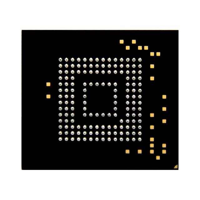
8. Ball Assignments
8.1. 153 Ball Package
Figure 24 – 153 ball assignment
___________________________________________________________________________________________________________________
© 2020 | Delkin Devices Inc.
40
�INDUSTRIAL EMBEDDED MULTIMEDIA CARD (EMMC)
401-0410-00 Rev F
9. Temperature
Parameter
Rating
Units
Operating temperature
-40 ~ +85
°C
Storage temperature
-40 ~ +85
°C
10. Ordering Information
Capacity/Type
Package Type
Delkin Part Number
Packaging
EM04APYD3-BA000-2
Trays
8GB MLC
EM08APGD3-BA000-2
1520 per box
10 trays of 152
MOQ 1 box
2GB pSLC
EM02APYD4-BA000-2
Trays
EM04APGD4-BA000-2
1520 per box
10 trays of 152
MOQ 1 box
4GB MLC
153 Ball
11.5x13x1.0
153 Ball
11.5x13x1.0
4GB pSLC
WARNING: This product may contain chemicals known to the State of California to cause cancer,
birth defects, or other reproductive harm. For more information go to www.p65warnings.ca.gov.
___________________________________________________________________________________________________________________
© 2020 | Delkin Devices Inc.
41
�


 工商网监
湘ICP备2023018690号
工商网监
湘ICP备2023018690号
