LS7272E
LS7272E-F
LS7273E
LS7272E-20
LS7273E-20
30 VOLT QUAD-CHANNEL DIFFERENTIAL LINE DRIVER
January 2020
PIN ASSIGNMENT – TOP VIEW
A 1
16 VDD
AO 2
15 D
AO 3
14 DO
LS7272E
More feature-rich and cost-effective than the OL7272 and ET7273
Pin to pin replaceable with the OL7272 and functionally equivalent to the ET7273
Push-Pull or Open-Drain output drivers (LS7272E)
Open-Drain output drivers only (LS7273E)
Voltage Range: 4.5V – 30V (VDD – VSS)
120mA Sink/Source output drive
Operating frequency up to 2 MHz
Thermal shutdown protection for output driver overload
Enable input with Thermal Shutdown disconnect feature
Outputs RS422A compatible
Inputs CMOS/TTL compatible with hysteresis
Output drivers fully connected or high-impedance state
PART NUMBER ORDERING INFORMATION:
This part is available in three package styles, DIP, SOIC, and TSSOP.
For DIP packages:
LS7273E,
LS7272E-20,
LS7272E, LS7272E-F,
LS7273E-20 For SOIC packages: LS7272E-S, LS7272E-F-S, LS7273E-S,
LS7272E-S20, LS7273E-S20 For TSSOP packages: LS7272E-TS, LS7272E-F-TS,
LS7273E-TS, LS7272ETS20, LS7273ETS20
LSI
LSI
FEATURES:
•
•
•
•
•
•
•
•
•
•
•
•
OPD 4
BO 5
6
11 CO
B
7
10 CO
VSS 8
FIGURE 1
The thermal shutdown block located in the center of the IC can be disabled by setting the ENA
input, Pin 12, to a voltage between 7.5V and 12V.
Upon power-up, a Power-On-Reset (POR) circuit block forces all output drivers to the highimpedance state until the power supply voltage reaches a nominal 3.8V. Included in the POR circuit
block is a hysteresis of 100mV such that if the power supply drops below 3.7V all output drivers are
forced to the high-impedance state until the voltage rises above 3.8V. There is a built-in 5μs delay
for disabling the output drivers should the power supply drop below 3.7V. The output drivers are
immediately enabled when the voltage rises above 3.8V.
7272E-012120-1
16 VDD
AO 2
15 D
AO 3
14 DO
n/c 4
BO 5
LS7272E-F
An internal 5V regulated supply is used to power the logic and level converter blocks.
A 1
LSI
For the LS7273, pin4 is LOW and is tied to ground. The outputs are open drain and the loads can be
returned to any voltage between 4.5V and 30V independent of VDD.
9 C
FIGURE 1
The LS7272E/LS7273E are short-circuit proof Quad Differential Industrial Power Line Drivers. They
can operate up to 30V and have a selectable thermal shutdown feature.
Pin4 is a no-connect in LS7272E-F. LS7272E-F has the outputs always in push-pull mode.
12 ENA
BO
DESCRIPTION:
The Data inputs are TTL / CMOS compatible and can also be driven up to the supply voltage VDD.
The ENA input can be used to place all the outputs in a high impedance state. For the LS7272E
the OPD input is used to connect the outputs as push-pull drivers or open-drain drivers, where
the outputs can be returned through external loads to a maximum voltage of VDD.
13 DO
13 DO
12 ENA
BO 6
11 CO
B
7
10 CO
VSS
8
9 C
FIGURE 1A
�16 VDD
20 VDD
VSS 2
19 D
A 1
LSI
1
LSI
A
LSI
A 1
20 VDD
VSS 2
19 D
18 n.c.
AO 3
18 n.c.
AO 3
14 DO
AO 4
17 DO
AO 4
17 DO
13 DO
n.c. 5
16 DO
n.c. 5
16 DO
12 ENA
BO 6
15 ENA
BO 6
BO 6
11 CO
BO 7
14 CO
BO 7
14 CO
B 7
10 CO
n.c. 8
13 CO
n.c. 8
13 CO
LOW
4
BO 5
VSS 8
9 C
B
12 VSS
9
n.c. 10
FIGURE 2
11 C
FIGURE 3
B
LS7273E-20
AO 3
LS7272E-20
15 D
LS7273E
AO 2
15 ENA
12 VSS
9
n.c. 10
11 C
FIGURE 4
NOTE: LS7272E-20 does not have OPD pin.
INPUT / OUTPUT DESCRIPTION:
A/B/ C/D
These are CMOS / TTL data inputs that can also operate with input levels up to the VDD power supply. All data input blocks contain hysteresis.
AO / BO / CO / DO / AO / BO / CO / DO
These outputs can be selected to be push-pull or open-drain using the OPD input pin (LS7272E only). When in push-pull mode, outputs switch
between VDD and VSS (Ground).
ENA
A logic low on this CMOS / TTL compatible input enables the output drivers while logic high forces them into a high-impedance state. This input is
also used to enable / disable the output short circuit thermal protection.
Applying a voltage between 7.5V and 12.5V to the ENA input will disable the thermal shutdown protection function. When using this feature, the Line
Driver Outputs are enabled but no longer protected.
OPD (LS7272E only)
A logic low on this connects the outputs as open-drain drivers. If this input is left floating, the outputs are connected as push-pull drivers.
LOW (LS7273E only)
This pin must be tied low.
7272E-012120-2
�VSS
VDD
A
B
C
D
ENA
n/c
(LS7272E-F)
5V
REGULATOR
CMOS / TTL
INPUT
LEVEL CONVERTER
DIFFERENTIAL
OUTPUT
BUFFER
CMOS / TTL
INPUT
LEVEL CONVERTER
DIFFERENTIAL
OUTPUT
BUFFER
CMOS / TTL
INPUT
LEVEL CONVERTER
DIFFERENTIAL
OUTPUT
BUFFER
CMOS / TTL
INPUT
LEVEL CONVERTER
DIFFERENTIAL
OUTPUT
BUFFER
LOGIC CONTROLLER
TRISTATE OUTPUTS
PUSH-PULL OR OPEN DRAIN OUTPUTS (LS7272E)
THERMAL SHUT DOWN
THERMAL SHUT DOWN DISABLE
UNDER VOLTAGE SHUT DOWN
POWER ON RESET
OPD
(LS7272E)
(LS7273E)
LOW
Should be tied Low.
7272-012120-3
FIGURE 4 LS7272E / LS7272E-F / LS7273E BLOCK DIAGRAM
AO
AO
BO
BO
CO
CO
DO
DO
�ABSOLUTE MAXIMUM RATINGS
Parameter
Symbol
Value
Unit
DC Supply Voltage
VDD
36
V
Data Output Voltage
VOUT
VDD + 0.3
V
Data Output Voltage
VOUT
4.5 to 36
V
Drive Output Current per output
IOUT
120
Data Input Voltage
VIND
VDD + 0.3
V
ENA Input Voltage
VINE
18
V
OPD Input Voltage
VINO
5
V
LOW Input Voltage
VINL
5
V
Operating Temperature
TA
-55 to +125
°C
Storage Temperature
TSTG
-65 to +150
°C
Applicable only to LS7273.
mA average
Applicable only to LS7272E.
Applicable only to LS7273E.
RECOMMENDED OPERATING CONDITIONS
Parameter
Symbol
Value
Unit
DC Supply Voltage
VDD
4.5 to 30
V
Data Input Voltage
VIND
0 to VDD
V
ENA Input Voltage
VINE
0 to 5.5
V
Data Output Voltage
VOUT
0 to VDD
V
Data Output Voltage
VOUT
4.5 to 30
V (LS7273E)
Data Output Current per output
IOUT
100
Operating Temperature
TOP
-40 to +125
°C
OPD
VINO
0 to float
V (LS7272E)
LOW
VINL
0
V (LS7273E)
7272E-012120-4
mA
See load characteristics
�ELECTRICAL CHARACTERISTICS
(VDD = 12V, TA = 25°C, unless otherwise specified)
Parameter
Symbol
Min
Typ
Max
Unit
Conditions
Data Input High-Threshold
VDH
-
1.7
2.4
V
ENA ≤ 0.8V
Data Input Low Threshold
VDL
0.8
1.2
-
V
ENA ≤ 0.8V
Data Input Hysteresis
VDHY
-
0.5
-
V
ENA ≤ 0.8V
ENA / OPD Input High-Threshold
VEH
-
1.7
2.4
V
-
ENA / OPD Input Low-Threshold
VEL
0.8
1.2
-
V
-
ENA / OPD Input Hysteresis
VEHY
-
0.5
-
V
-
Leakage Current
ILKG
-5
+5
μA
ENA
IESO
-
OPD, LOW
IDSI
-30
VOH
VDD – 0.4
VOH
VDD – 0.6
Inputs:
Inputs:
μA
ENA = 12V
μA
OPD , LOW= 0V
V
ILOAD = 20mA, VDD = 4.75V
-
V
ILOAD = 30mA, VDD = 30V
100
-
Outputs:
High-Level Output Voltage
(LS7272E only)
Output Resistance
RDSON
-
20
-
Ω
ILOAD = 30mA
Low Voltage Output Voltage
VOL
-
0.3
-
V
ILOAD = -20mA, VDD = 4.75V
VOL
-
0.4
-
V
ILOAD = -30mA, VDD = 30V
IDD
6
-
15
mA
IOT
-10
+10
μA
VDD = 20V, 2.4V < ENA < 7.5V
Power-On-Reset (POR)
VPOR
-
V
-
POR Hysteresis
VPORH
POR Removal Time
TPORR
Quiescent Current
High-Impedance Output
Leakage Current (Outputs Disabled)
Reset:
-
3.6
0.1
-
V
-
5
-
μS
-
165
185
°C
Over-Temperature Protection:
Junction Temperature Operate Point
TJTO
Junction Temperature Release Point
TJTR
100
ENA Input (Over Temp Protection Inhibit)
VEPI
7.0
°C
135
12.5
V
NOTE 1: When the thermal shutdown is inhibited, the driver might be destroyed if it is not operated within its normal operating conditions.
NOTE 2: Add 0.1uF to OPD input when the device is used in push-pull mode.
7272E-012120-5
�AC SWITCHING CHARACTERISTICS
(VDD = 12V, TA = 25°C, Load Capacitance = 1000 pF)
Parameter
Propagation delay from 50% point of input
rising edge to zero crossing of differential
outputs
Symbol
Min
Typ
Max
Unit
Conditions
TPLH
-
105
150
ns
VDD = 5V (LS7272E only)
-
112
200
ns
VDD = 12V (LS7272E only)
-
135
250
ns
VDD = 24V (LS7272E only)
-
105
150
ns
VDD = 5V
-
112
280
ns
VDD = 12V
-
135
330
ns
VDD = 24V
-
64
125
ns
VDD = 5V (LS7272E only)
-
75
150
ns
VDD = 12V (LS7272E only)
-
98
175
ns
VDD = 24V (LS7272E only)
-
65
125
ns
VDD = 5V
-
73
175
ns
VDD = 12V
-
101
250
ns
VDD = 24V
TPHL
Propagation delay from 50% point of input
rising edge to zero crossing of differential
outputs
Output Rise Time
Output Fall Time
TR
TF
ENA Enable Time
TON
-
60
200
ns
-
ENA Disable Time
TOFF
-
80
200
ns
-
The information included herein is believed to be accurate and
reliable. However, LSI Computer Systems, Inc. assumes no
responsibilities for inaccuracies, or for any infringements of
patent rights of others which may result from its use.
7272E-012120-6
�E
*NOTE: Add series resistors (Rs) in case of abnormal situation where any of the LS7272E’s outputs are subject
to voltages when either power pins are not connected. See table below.
VDD
≤ 10V
10V ≤ VDD ≤ 15V
15V ≤ VDD ≤ 30V
7272E-012120-7
Rs
≥ 10Ω
≥ 25Ω
≥ 50Ω
�
很抱歉,暂时无法提供与“LS7272E-S”相匹配的价格&库存,您可以联系我们找货
免费人工找货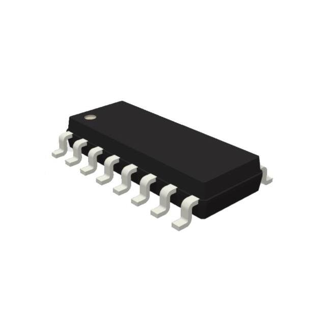


 工商网监
湘ICP备2023018690号
工商网监
湘ICP备2023018690号
