Advanced Science And Novel Technology Company, Inc.
2790 Skypark Drive Suite 112, Torrance, CA 90505
Offices: 310-530-9400 / Fax: 310-530-9402
www.adsantec.com
ASNT8160-KMF
Programmable CR
Up to 65Gb/s half-rate clock recovery circuit
CR range from 25.5GHz to 32.5GHz covered by 3 selectable VCOs
NRZ input data format
CML compliant differential input and output high-speed data and clock interfaces
LVDS compliant input reference clock interface
Half rate clock output up to 32.5GHz for a 65Gb/s input data signal
Single +3.3V or -3.3V power supply
Low power consumption of 1.6W at the maximum operational speed
Industrial temperature range
Custom CQFP 64-pin package
ASNT 8160
Rev. 1.3.2
1
May 2020
�Advanced Science And Novel Technology Company, Inc.
2790 Skypark Drive Suite 112, Torrance, CA 90505
Offices: 310-530-9400 / Fax: 310-530-9402
www.adsantec.com
DESCRIPTION
phshft
Fig. 1. Functional Block Diagram
ASNT8160-KMF is a half-rate integrated clock recovery (CR) circuit. The IC shown in Fig. 1 functions
in the CR mode covering a wide range of input data rates (fbit) by utilizing its three on-chip VCOs
(voltage-controlled oscillators). Selection of the desired working data rate and mode is accomplished
through pins vcos0 and vcos1 (see Table 1). An external low speed system clock c32p/c32n running at
1/32 the frequency of the active VCO must be applied to the low-speed LVDS clock input buffer (CLK
IB) for the IC to work properly.
The main function of the chip is to recover from an NRZ input data signal dp/dn with a bit rate of fbit
accepted by CML buffer (Data IB) a half-rate clock c2p/c2n that is delivered to the output by the CML
clock output buffer (COB). For example, a 30GHz clock signal will be generated from a 60Gb/s input
data signal. The signal phshft is used to properly set the phase of the internal clock.
Data IB can operate with either differential or single-ended input signals. It includes tuning pins
dcinp/dcinn for DC offset of the input signals in case of AC termination. When the buffer is operating
Rev. 1.3.2
2
May 2020
�Advanced Science And Novel Technology Company, Inc.
2790 Skypark Drive Suite 112, Torrance, CA 90505
Offices: 310-530-9400 / Fax: 310-530-9402
www.adsantec.com
with a DC-terminated single ended input signal, a correct threshold voltage should be applied to the
unused input pin.
All CML I/Os provide on chip 50Ohm termination to vcc and may be used differentially, AC/DC
coupled, single-ended, or in any combination (see also POWER SUPPLY CONFIGURATION).
A loss of lock CMOS alarm signal lolp is generated by the CR to indicate its locking state. An off chip
passive filter is required by the CR, and should be connected to pin ftr (see CR section).
The clock recovery circuit is characterized for operation from 0°C to 125°C of junction temperature. The
package temperature resistance is 15°C /W.
Data IB
The Data Input Buffer (Data IB) can process an input CML data signal dp/dn in NRZ format. It provides
on-chip single-ended termination of 50Ohm to vcc for each input line. The buffer can also accept a singleended signal to one of its input ports dp or dn with a threshold voltage applied to the unused pin in case
of DC termination. In case of AC termination, tuning pins dcinp/dcinn allow for data common mode
adjustment. The tuning pins have 1KOhm terminations to vcc and allow the user to change the slicing
level before the data is sent to the clock recovery section. Tuning voltages from vcc to vee deliver 150mV
of DC voltage shift.
HS CIB
The High-Speed Clock Input Buffer (HS CIB) can process either differential or single-ended external
CML clock signals cep/cen. In single-ended mode, the clock is applied to one of the pins together with a
threshold voltage applied to the unused pin. The buffer utilizes on-chip single-ended termination of
50Ohm to vcc for each input line. This functionality is for test purposes only.
CLK IB
The Clock Input Buffer (CLK IB) consists of a proprietary universal input buffer (UIB) that exceeds
LVDS standards IEEE Std. 1596.3-1996 and ANSI/TIA/EIA-644-1995. UIB is designed to accept
differential signals with a speed up to 1Gb/s, DC common mode voltage variation between vcc and vee,
AC common mode noise with a frequency up to 5MHz, and voltage levels ranging from 0 to 2.4V. It can
also receive a DC-terminated single-ended signal with a threshold voltage between vcc and vee applied
to the unused pin. The input termination impedance is set to 100Ohm differential.
CR
The Clock Recovery Block (CR) contains both a phase and frequency acquisition loop. The frequency
loop works in concert with low-speed clock c32p/c32n while the phase loop utilizes data signal dp/dn.
The CR requires a single off-chip filter shown in Fig. 2 to be connected to pin ftr.
200Ohm
ftr
100pF
1nF
Fig. 2. External Loop Filter
Rev. 1.3.2
3
May 2020
�Advanced Science And Novel Technology Company, Inc.
2790 Skypark Drive Suite 112, Torrance, CA 90505
Offices: 310-530-9400 / Fax: 310-530-9402
www.adsantec.com
The main function of the CR is to frequency-lock the selected on-chip VCO to the input data signal (clock
recovery). Using the external control voltage phshft within the range from vcc to vcc-1.0V, the phase of
the internal half rate clock needs to be lined up correctly with the incoming data in the phase loop to
ensure proper CR functionality.
By utilizing the 2.5V CMOS control pins vcos0 and vcos1, the desired working frequency of the CR can
be selected in accordance with Table 1 below.
Table 1. CR Mode Selection (Case Temperature from 0 to 90°C)
vcos0
vcos1
VCO Operation Frequency (GHz)
“0” (0V)
“0” (0V)
fmin≤25.5, fmax≥28.0
“0” (0V) ”1” (2.5V)
fmin≤27.5, fmax≥29.5
”1” (2.5V) “0” (0V)
fmin≤29.0, fmax≥32.5
”1” (2.5V) ”1” (2.5V)
Digital Mode, default state
The loop gain can be adjusted by two 2.5V CMOS control pins icph and icpl that control the charge pump
current as shown in Table 2.
Table 2. Charge Pump Current Control
icph
icpl
Charge Pump current, mA
“0” (0V)
“0” (0V)
Imax
“0” (0V) ”1” (2.5V)
Imax-0.04
”1” (2.5V) “0” (0V)
Imax-0.27
”1” (2.5V) ”1” (2.5V)
Imax-0.31
The lock detect circuitry signals an alarm through the 2.5V CMOS signal lolp when a frequency
difference exists between an applied system reference clock c32p/c32n and a recovered half rate clock
divided-by-32 that is greater than ±1000ppm.
COB
The Clock Output Buffer (COB) receives a half rate clock signal from CR and converts it into CML
output signal c2p/c2n. The buffer requires 50Ohm external termination resistors connected between vcc
and each output (usually supplied by the downstream chip that the buffer is driving).
POWER SUPPLY CONFIGURATION
The ASNT8160-KMF can operate with either a negative supply (vcc = 0.0V = ground and vee = -3.3V),
or a positive supply (vcc = +3.3V and vee = 0.0V = ground). In case of a positive supply, all I/Os need
AC termination when connected to any devices with 50Ohm termination to ground. Different PCB layouts
will be needed for each different power supply combination.
All the characteristics detailed below assume vcc = 3.3V and vee = 0V (external
ground)
Rev. 1.3.2
4
May 2020
�Advanced Science And Novel Technology Company, Inc.
2790 Skypark Drive Suite 112, Torrance, CA 90505
Offices: 310-530-9400 / Fax: 310-530-9402
www.adsantec.com
ABSOLUTE MAXIMUM RATINGS
Caution: Exceeding the absolute maximum ratings shown in Table 3 may cause damage to this product
and/or lead to reduced reliability. Functional performance is specified over the recommended operating
conditions for power supply and temperature only. AC and DC device characteristics at or beyond the
absolute maximum ratings are not assumed or implied. All min and max voltage limits are referenced to
ground (assumed vee).
Table 3. Absolute Maximum Ratings
Parameter
Supply Voltage (vcc)
Power Consumption
Input Voltage Swing (SE)
Case Temperature*)
Storage Temperature
Operational Humidity
Storage Humidity
Min
-40
10
10
Max
+3.8
1.6
1.0
+90
+100
98
98
Units
V
W
V
ºC
ºC
%
%
TERMINAL FUNCTIONS
Name
vcc
vee
nc
Supply and Termination Voltages
Description
Pin Number
Positive power supply (+3.3V)
2, 4, 6, 11, 13, 15, 18, 20, 22, 27, 29, 31, 34, 36,
38, 43, 45, 47, 54, 55, 57, 59, 60
Negative power supply (GND or 0V)
1, 16, 17, 32, 33, 48, 49, 50, 63, 64
Not connected pins
19, 26, 30, 35, 37, 39, 40, 41, 42, 44, 46, 51, 52
TERMINAL
Name
No.
Type
cep
cen
c2p
c2n
dp
dn
3
5
28
21
56
58
c32p
c32n
12
14
vcos1
vcos0
is
icpl
Rev. 1.3.2
Input
Output
Input
Input
DESCRIPTION
High-Speed I/Os
CML differential half rate clock inputs with internal SE 50Ohm
termination to vcc
CML differential half rate clock outputs. Require external SE 50Ohm
termination to vcc
CML differential data inputs with internal SE 50Ohm termination to
vcc
Low-Speed I/Os
LVDS clock input with internal differential 100Ohm termination
Controls
CR operational mode selection, see Table 1
7
LS In.,
10 2.5V CMOS
9
VCO current control (high, default: higher current; low: lower current)
23
Charge pump current control, see Table 2
5
May 2020
�Advanced Science And Novel Technology Company, Inc.
2790 Skypark Drive Suite 112, Torrance, CA 90505
Offices: 310-530-9400 / Fax: 310-530-9402
www.adsantec.com
icph
lolp
24
25
dcinp
dcinn
phshft
ftr
LS out,
CR lock indicator (high: no lock; low: locked)
2.5V CMOS
53
LS IN
Input data common mode voltage adjustment
61
62
DC Input CR clock phase adjustment. Allowed values from vcc to vcc-1.0V
8
I/O
External CR filter connection
ELECTRICAL CHARACTERISTICS
PARAMETER
TYP MAX
UNIT
COMMENTS
General Parameters
+3.0
+3.3
+3.6
V
±9%
vcc
0.0
V
vee
Ivcc
490
mA
All functions active
Power Consumption
1.6
W
Junction Temperature
-25
50
125
°C
Case temperature
75
°C
Recommended value
HS Input Data (dp/dn)
Data Rate
51
65
Gbps
RZ or NRZ
Swing p-p (Diff or SE)
0.3
0.6
V
at 65Gbps
CM Voltage Level
vcc-0.8
vcc
V
LS Input Reference Clock (c32p/c32n)
Frequency
796
1016
MHz
Swing p-p (Diff or SE)
0.06
0.8
V
CM Voltage Level
V
vee
vcc
Duty Cycle
40
50
60
%
HS Output Half Rate Clock (c2p/c2n)
Clock Rate
25.5
32.5
GHz
50 to 64Gbps input
Logic “1” level
V
vcc
Logic “0” level
vcc -0.4
vcc -0.15
V
Jitter
5
8
ps
p-p at 25.6GHz
Input Data Common Mode Control (dcinp/dcinn)
Input DC Voltage
V
vee
vcc
Input Data Voltage Shift
0
-150
mV
Referenced to vcc
CMOS Control Inputs/Outputs
Logic “1” level
2.1
2.5
V
Logic “0” level
vee +0.4
V
Data Sampling Point Adjustment (phshft)
Internal termination
1.8
kOhm
SE to vcc
Input DC Voltage
vcc -1.0
vcc
V
Bandwidth
0.0
100
MHz
Rev. 1.3.2
MIN
6
May 2020
�Advanced Science And Novel Technology Company, Inc.
2790 Skypark Drive Suite 112, Torrance, CA 90505
Offices: 310-530-9400 / Fax: 310-530-9402
www.adsantec.com
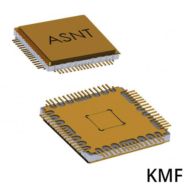
PACKAGE INFORMATION
The chip die is housed in a custom 64-pin CQFP package. The dimensioned drawings are shown in Fig. 3.
The package provides a center heat slug located on its back side to be used for heat dissipation.
ADSANTEC recommends for this section to be soldered to the vcc plain, which is ground for a negative
supply, or power for a positive supply.
The part’s identification label is ASNT8160-KMF. The first 8 characters of the name before the dash
identify the bare die including general circuit family, fabrication technology, specific circuit type, and part
version while the 3 characters after the dash represent the package’s manufacturer, type, and pin out
count.
This device complies with the Restriction of Hazardous Substances (RoHS) per 2011/65/EU for all ten
substances.
Fig. 3. CQFP 64-Pin Package Drawing (All Dimensions in mm)
Rev. 1.3.2
7
May 2020
�Advanced Science And Novel Technology Company, Inc.
2790 Skypark Drive Suite 112, Torrance, CA 90505
Offices: 310-530-9400 / Fax: 310-530-9402
www.adsantec.com
REVISION HISTORY
Revision
1.3.2
1.2.2
1.2.1
Date
05-2020
07-2019
08-2015
1.1.1
05-2015
1.0.0
03-2015
Rev. 1.3.2
Changes
Updated Package Information
Updated Letterhead
Revised pin out drawing
Revised block diagram
Added text to Description section
Added information to Terminal Functions & Electrical Specifications
Revised package information section
Corrected format
Preliminary release
Part number changed from ASNT2117-KMF to ASNT8160-KMF
8
May 2020
�


 工商网监
湘ICP备2023018690号
工商网监
湘ICP备2023018690号
