TS393
Taiwan Semiconductor
Low Power Low Offset Voltage Dual Comparators
GENERAL DESCRIPTION
FEATURES
The TS393 is dual independent precision voltage
●
comparators capable of single-supply or split-supply
Output voltage compatible with DTL, ECL, TTL,
MOS and CMOS Logic levels
operation. The specifications as low as 2.0 mV make
●
Low input bias current 25nA
this device an excellent ground level with single-supply
●
Low input offset current ±0.5nA
operation. Input offset-voltage selection for many
●
Low input offset voltage ±2mV (typ)
applications in consumer automotive, and It is designed
●
Input common mode range to ground level
to
●
Differential input voltage range equal to power
permit
a
common
mode
range-to-
industrial
electronics.
supply voltage
●
Very low supply current drain (0.4mA) –
independent of supply voltage
DIP-8
●
Wide single-supply range 2V~36V
●
Split- supply range ±1V to ±18V
SOP-8
Pin Definition:
1. Output A
2. Input A (-)
3. Input A (+)
4. GND
5. Input B (+)
6. Input B (-)
7. Output B
8. VCC
Notes: Moisture sensitivity level: level 3. Per J-STD-020
TYPICAL APPLICATIN CIRCUIT
Zero Crossing Detector (Single Supply)
Document Number: DS_P0000198
1
Version: B15
�TS393
Taiwan Semiconductor
ABSOLUTE MAXIMUM RATINGS (TA = 25°C unless otherwise noted) (Note 1)
PARAMETER
SYMBOL
LIMIT
UNIT
Supply Voltage
VCC
+36 or ±18
V
Differential Input Voltage
VIDR
36
V
Input Common Mode Voltage Range
VICR
-0.3 to 36
V
Input Current
IIN
50
mA
Output Short Circuit to Ground
ISC
Continuous
Output Sink Current
ISINK
20
mA
Operating Temperature Range
TOPR
0 ~ +70
°C
TJ
150
°C
Storage Temperature Range
TSTG
-65 ~ +150
°C
Lead Temperature 1.6mm (1/16”) from case for 10s.
TLEAD
260
°C
Junction Temperature
ELECTRICAL CHARACTERISTICS (VCC = 5V, TA = 25°C unless otherwise noted)
PARAMETER
Input Offset Voltage
(note 3)
Input Offset Current
IIN(+) - IIN(-), VCM=0V
Input Offset Current
SYMBOL
MIN
TYP
MAX
UNIT
VIO
--
2
5
mV
IIO
--
--
50
nA
IIB
--
--
250
nA
VICR
-0
--
VCC-1.5
V
AVOL
50
200
--
V/mV
--
--
300
--
ns
tTLH
--
1.3
--
µs
ISINK
6.0
16
--
mA
VOL
--
250
400
mV
IOL
--
0.1
--
nA
ICC
--
0.4
1.0
mA
--
1.0
2.5
(note 4)
IIN(+) - IIN(-), VCM=0V
Input Common Mode Voltage Range
(note 5)
VCC=30V
Voltage Gain
RL ≥15K, VCC =15V, Vo=1V~11V
Large Signal Response Time
Vin=TTL Logic Swing. VREF = 1.4V,
VRL=5V. RL=5.1kΩ
Response Time
(note 6)
VRL=5V. RL=5.1kΩ
Output Sink Current
VIN(-)=1V, VIN(+)=0V, Vo≤1.5V
Output Saturation Voltage
VIN(-)=1V, VIN(+)=0V, ISINK≤4mA
Output Leakage Current
VIN(-)=0V, VIN(+)=1V, Vo=5V
Supply Current
RL = ∞, VCC =5V
RL = ∞, VCC =36V
Document Number: DS_P0000198
2
Version: B15
�TS393
Taiwan Semiconductor
ELECTRICAL CHARACTERISTICS
Note:
1.
The max. Output current may be as high as 20mA, independent of the magnitude of VCC, output short circuits to VCC can
cause excessive heating and eventual destruction.
2.
This magnitude of input current will only occur if the input leads are driven more negative than ground or the negative
supply voltage. This is due to the input PNP collector base junction becoming forward biased acting as an input clamp
diode. There is also a lateral PNP parasitic transistor action on the IC chip. This phenomenon can cause the output voltage
of the comparators to go to the VCC voltage level (or ground if overdrive is large) during the time the input is driven negative.
This will not destroy the device and normal output states will recover when the inputs become -0.3V of ground or negative
supply.
3.
At output switch point, VO=1.4Vdc, RS=0Ω with VCC from 5Vdc to 30Vdc, and over the full input common-mode
4.
Due to the PNP transistor inputs, bias current will flow out of the inputs, this current is essentially constant independent of
5.
Input common mode of either input should not be permitted to go more than 0.3V negative of ground or minus supply. The
the output state, therefore, no loading changes will exist on the input lines.
upper limit of common mode range is VCC - 1.5V but either or both inputs can be taken to as high as 30volts without
damage.
6.
Response time is specified with a 100mV step and 5.0mV of overdrive. With larger magnitudes of overdrive faster response
times are obtainable.
ORDERING INFORMATION
PART NO.
PACKAGE
PACKING
TS393CD C3G
DIP-8
50pcs / Tube
TS393CS RLG
SOP-8
2,500pcs / 13” Reel
Note:
1. Compliant to RoHS Directive 2011/65/EU and in accordance to WEEE 2002/96/EC.
2. Halogen-free according to IEC 61249-2-21 definition.
BLOCK DIAGRAM
Document Number: DS_P0000198
3
Version: B15
�TS393
Taiwan Semiconductor
ELECTRICAL CHARACTERISTICS CURVE
Figure 1. Input Bias Current vs.
Power Supply Voltage
Figure 2. Output Saturation Voltage vs.
Output Sink Current
Figure 3. Power Supply Current vs.
Power Supply Voltage
Document Number: DS_P0000198
4
Version: B15
�TS393
Taiwan Semiconductor
APPLICATION INFORMATION
This dual comparator feature high gain, wide bandwidth characteristics. This gives the device oscillation tendencies
if the outputs are capacitive coupled to the inputs via stray capacitance. This oscillation manifests itself during
output transitions (VOL to VOH). To alleviate this situation input resistors
很抱歉,暂时无法提供与“TS393CS RLG”相匹配的价格&库存,您可以联系我们找货
免费人工找货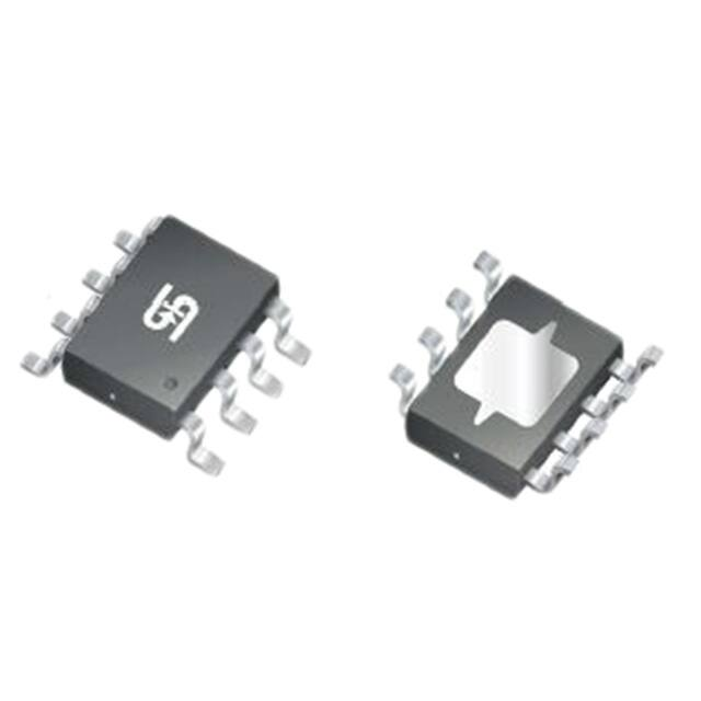


 工商网监
湘ICP备2023018690号
工商网监
湘ICP备2023018690号
