NJU7116
SUPER LOW OPERATING CURRENT AND LOW OFFSET VOLTAGE
TINY SINGLE CMOS COMPARATOR
■ GENERAL DESCRIPTION
■ PACKAGE OUTLINE
The NJU7116 is a super low operating current and low offset voltage
tiny single CMOS comparator with CMOS output.
The operating current is 1μA ( typ ), and the operating of 1.8V to
3.6V.
The input offset voltage is lower than 2.5mV ( max ).
Furthermore, the NJU7116 is packaged with very small SOT−23−5
NJU7116F
DFN6-G1; therefore it can be especially applied to battery operated
portable items.
■ FEATURES
● Super Low Operating Current
● Single Power Supply
● Low Offset Voltage
● Low Bias Current
● CMOS ( Push-pull ) Output
● Package Outline
● CMOS Technology
NJU7116KG1
■ PIN CONFIGURATION
( IDD=1.0μA typ. )
( VDD=1.8 to 3.6V )
( VIO=2.5mV max.@ 3.0V )
( IIB=1pA typ. )
(Top View)
SOT−23−5, DFN6-G1
NJU7116F
(Top View)
(Bottom View)
NJU7116KG1
NJU7116KG1
The NC pin and the PAD should connect with a VSS
terminal.
■ EQUIVALENT CIRCUIT
Ver.2016-07-04
-1-
�NJU7116
■ ABSOLUTE MAXIMUM RATINGS
( Ta=25˚C )
PARAMETER
Supply Voltage
Differential Input Voltage
Common Mode Input Voltage
Power Dissipation
SYMBOL
VDD
VID
VIC
RATINGS
7
± 7 ( note1)
-0.3 to 7( note1)
UNIT
V
V
V
PD
390 (note 3) / 520 (note 4)
260 (note 5) / 950 (note 6)
-40 to +105
-55 to +125
mW
SOT-23-5
DFN6-G1
Operating Temperature Range
Storage Temperature Range
Topr
Tstg
˚C
˚C
( note1) For supply voltage less than 7V, the absolute maximum rating is equal to the supply voltage.
( note2 ) Decoupling capacitor should be connected between VDD and VSS due to the stabilized operation for the circuit.
( note3 ) EIA/JEDEC STANDARD Test board (76.2x114.3x1.6mm, 2layers, FR-4) mounting
( note4 ) EIA/JEDEC STANDARD Test board (76.2x114.3x1.6mm, 4layers, FR-4) mounting
( note5 ) Mounted on glass epoxy board. (101.5×114.5×1.6mm: based on EIA/JEDEC standard, 2Layers FR-4, with Exposed Pad)
( note6 ) Mounted on glass epoxy board. (101.5×114.5×1.6mm: based on EIA/JEDEC standard, 4Layers FR-4, with Exposed Pad)
(For 4Layers: Applying 99.5×99.5mm inner Cu area and a thermal via hole to a board based on JEDEC standard JESD51-5)
( note7 ) The NC pin and the PAD should connect with a VSS terminal.
( note8 ) The NC pin is electrically not connected to the die in a package.
( note9 ) The PAD is electrically connected to the backside of the die. The PAD cannot be used as VSS terminal.
■ ELECTRICAL CHARACTERISTICS
( Ta=25˚C,VDD=3.0V,RL=∞ )
PARAMETER
Operating Voltage
Input Offset Voltage
Input Offset Current
Input Bias Current
Input Common Mode Voltage Range
High Level Output Voltage
Low Level Output Voltage
Common Mode Rejection Ratio
Supply Voltage Rejection Ratio
Operating Current
SYMBOL
VDD
VIO
IIO
IIB
VICM
VOH
VOL
CMR
SVR
IDD
TEST CONDITION
VIN=1/2VDD
IOH=2mA
IOL=-2mA
VIC=1/2VDD
VDD=1.8~3.6V
No Load,VO=0V
MIN.
1.8
0~2.5
2.7
50
50
-
TYP.
1
1
1
MAX.
3.6
2.5
0.3
1.5
UNIT
V
mV
pA
pA
V
V
V
dB
dB
μA
■ SWITCHING CHARACTERISTICS
( Ta=25˚C,VDD=3.0V,f=1kHz,CL=15pF )
PARAMETER
Propagation Delay
High to Low
Propagation Delay
Low to High
Propagation Delay
Time Lag
Output Signal
Falling Time
Output Signal
Rising Time
-2-
SYMBOL
tPHL
tPLH
CONDITIONS
Over Drive=100mV
VIC=0V
TTL Level Step In.
Over Drive=100mV
VIC=0V
TTL Level Step In.
MIN
-
TYP
1.2
0.37
3.3
2.6
MAX
2.0
5.0
-
UNIT
μs
μs
tPD
tPLH- tPHL
-
2.1
3.0
μs
tTHL
Over Drive=100mV
-
15
-
ns
tTLH
Over Drive=100mV
-
40
-
ns
Ver.2016-07-04
�NJU7116
■ TYPICAL CHARACTERISTICS
Operating Current vs. Operating Voltage
1.3
VSS=0V, VIN+=VDD/2
3
1.2
Operating Current [μA]
Operating Current [μA]
Operating Current vs. Temperature
VSS=0V, VIN+=VDD/2
1.1
1
0.9
2
VDD=3V
1
VDD=1.8V
0.8
0
1.8
2.4
3
Supply Voltage VDD [V]
3.6
-50
Input Offset Voltage vs. Temperature
14
2
Input Offset Voltage [mV]
Input Offset Voltage [mV]
VSS=0V, VIN+=0V
16
VDD=1.8V
1
0
VDD=3V
-1
-2
12
10
8
VDD=1.8V
6
VDD=3V
4
2
0
-3
-2
-50
0
50
100
Ambient Temperature [ºC]
150
-50
Input Offset Voltage vs. Operating Voltage
Input Offset Voltage [mV]
6
Ta=-40ºC
Ta=105ºC
4
Ta=25ºC
2
0
-2
150
VSS=0V, VIN+=0V
18
8
0
50
100
Ambient Temperature [ºC]
Input Offset Voltage vs. Operating Voltage
VSS=0V, VIN+=VDD/2
10
Input Offset Voltage [mV]
150
Input Offset Voltage vs. Temperature
VSS=0V, VIN+=VDD/2
3
0
50
100
Ambient Temperature [ºC]
14
10
Ta=-40ºC
6
Ta=25ºC
Ta=105ºC
2
-2
1.8
Ver.2016-07-04
2.4
3
Operating Voltage VDD [V]
3.6
1.8
2.4
3
Operating Voltage VDD [V]
3.6
-3-
�NJU7116
■ TYPICAL CHARACTERISTICS
Output Source Current vs. Temperature
6
VSS=0V, VOL=VSS+0.3V
6
5
Output Sink Current [mA]
Output Source Current [mA]
Output Sink Current vs. Temperature
VSS=0V, VOH=VDD-0.3V
4
VDD=3V
3
2
1
5
VDD=3V
4
3
2
1
VDD=1.8V
VDD=1.8V
0
-50
0
50
100
Ambient Temperature [ºC]
0
150
-50
Propagation Delay vs. Temperature
Propagation Delay(High to Low) [μs]
Propagation Delay(Low to High) [μs]
VDD=3.0V, VSS=0V, VIN-=VDD/2, Vod=100mV, CL=15pF
2
6
5
4
3
2
1
0
-50
-4-
150
Propagation Delay vs. Temperature
VDD=3.0V, VSS=0V, VIN-=VDD/2, Vod=100mV, CL=15pF
7
0
50
100
Ambient Temperature [ºC]
0
50
100
Ambient Temperature [ºC]
150
-50
0
50
100
Ambient Temperature [ºC]
150
Ver.2016-07-04
�NJU7116
■ SWITCHING CHARACTERISTICS MEASUREMENT CIRCUIT
■ TIMING WAVEFORM
Ver.2016-07-04
-5-
�NJU7116
■ PACKAGE DIMENSIONS
2.9±0.2
0°~15°
1
2
2.8 ±0.2
0.6
4
+0.2
1.6 - 0.1
5
0.2MIN
1.9±0.2
3
0.95±0.1
+0.1
0.1-0.03
0.4±0.1
0.1
Unit: mm
0.1MAX
1.1±0.1
0.6MAX
SOT-23-5 Package
-6-
Ver.2016-07-04
�NJU7116
■ PACKAGE DIMENSIONS
Unit: mm
DFN6-G1 Package
Ver.2016-07-04
[CAUTION]
The specifications on this databook are only
given for information , without any guarantee
as regards either mistakes or omissions. The
application circuits in this databook are
described only to show representative usages
of the product and not intended for the
guarantee or permission of any right including
the industrial rights.
-7-
�
很抱歉,暂时无法提供与“NJU7116F-TE1”相匹配的价格&库存,您可以联系我们找货
免费人工找货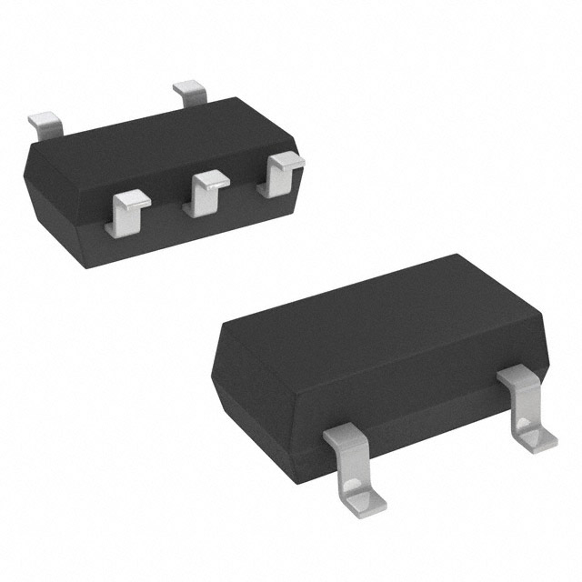


 工商网监
湘ICP备2023018690号
工商网监
湘ICP备2023018690号
