LSI/CSI
UL
LS7083N
LS7084N
®
LSI Computer Systems, Inc. 1235 Walt Whitman Road, Melville, NY 11747
(631) 271-0400 FAX (631) 271-0405
A3800
June 2015
QUADRATURE CLOCK CONVERTER
VDD (Pin 2)
Supply Voltage positive terminal.
VSS (Pin 3)
Supply Voltage negative terminal.
A (Pin 4)
Quadrature Clock Input A. This input has a filter circuit to validate
input logic level and eliminate encoder dither.
B (Pin 5)
Quadrature Clock Input B. This input has a filter circuit identical
to input A.
Mode (Pin 6)
Mode is a 3-state input to select resolutions x1, x2 or x4. The selected resolution multiplies the input quadrature clock rate by 1, 2
and 4, respectively, in producing the outputs UPCK / DNCK and
CLK (see Figure 2).
The Mode input logic levels selects resolutions as follows:
Logic 0 = x1 Float = x2 Logic 1 = x4
7083N/84N-062315
-1
V DD (+V )
2
V SS (-V )
3
A
4
RBIAS
1
V DD (+V )
2
V SS (-V )
3
A
4
LS7084N
INPUT/OUTPUT DESCRIPTION:
RBIAS (Pin 1)
Input for external component connection. A resistor connected
between this input and VSS adjusts the output clock pulse width
(Tow). For proper operation, the output clock pulse width must be
less than or equal to the A, B pulse separation (TOW ≤ TPS).
1
LSI
DESCRIPTION:
The LS7083N and LS7084N are CMOS quadrature clock converters. Quadrature clocks derived from optical or magnetic encoders, when applied to the A and B inputs of the LS7083N or
LS7084N, are converted to strings of Up Clocks and Down
Clocks ( LS7083N) or to a Clock and an Up/Down direction control (LS7084N). These outputs can be interfaced directly with
standard Up/Down counters for direction and position sensing of
the encoder.
RBIAS
LS7083N
Applications:
• Interface incremental encoders to Up / Down Counters
(See Figure 6A and Figure 6B)
• Interface rotary encoders to Digital Potentiometers
(See Figure 7)
PIN ASSIGNMENT - TOP VIEW
LSI
FEATURES:
• x1 and x4 mode selection
• Up to 16MHz output clock frequency
• Programmable output clock pulse width
• On-chip filtering of inputs for optical or
magnetic encoder applications.
• TTL and CMOS compatible I/Os
• +3V to +12V operation (VDD - VSS)
• LS7083N, LS7084N (DIP);
LS7083NS, LS7084NS (SOIC) - See Figure 1
8
UPCK
7
DNCK
6
MODE
5
B
8
CLK
7
UP/DN
6
MODE
5
B
FIGURE 1
LS7083N - DNCK (Pin 7)
In LS7083N, this is the DOWN Clock Output. This output consists of
low-going pulses generated when A input lags the B input.
LS7084N - UP/DN (Pin 7)
In LS7084N, this is the count direction indication output. When A
input leads the B input, the UP/DN output goes high indicating that
the count direction is UP. When A input lags the B input, UP/DN
output goes low, indicating that the count direction is DOWN.
LS7083N - UPCK (Pin 8)
In LS7083N, this is the UP Clock output. This output consists of
low-going pulses generated when A input leads the B input.
LS7084N - CLK (Pin 8)
In LS7084N, this is the combined UP Clock and DOWN Clock output. The count direction at any instant is indicated by the UP/DN
output (Pin 7).
NOTE: For the LS7084N, the timing of CLK and UP/DN requires
that the counter interfacing with LS7084N counts on the rising edge
of the CLK pulses.
�ABSOLUTE MAXIMUM RATINGS:
PARAMETER
SYMBOL
DC Supply Voltage
VDD - VSS
16
V
Voltage at any input
VIN
VSS-0.3 to VDD+0.3
V
TA
-20 to +85
ºC
TSTG
-55 to 150
ºC
Operating temperature
Storage temperature
DC ELECTRICAL CHARACTERISTICS:
VALUE
UNITS
(Unless otherwise specified VDD = 3V to 12V and TA = -20ºC to +85ºC)
PARAMETER
SYMBOL
MIN
Supply Voltage
VDD
TYP
MAX
UNITS
CONDITION
3
-
12
V
Supply Current
IDD
-
1.5
1.65
mA
Logic 0
Vml
-
-
0.5
V
Logic 1
Vmh
VDD - 0.5
-
-
V
Logic Float
Vmf
(VDD/2) - 0.5
VDD/2
(VDD/2) + 0.5
V
-
Logic 0 Input Current
Iml
-
2.2
4.2
μA
VDD = 3V
Iml
-
3.5
6.9
μA
VDD = 5V
VDD = 12V, all input frequencies=0 Hz and RBIAS = 2MΩ
MODE INPUT:
Logic 1 Input Current
-
Iml
-
8.3
16.2
μA
VDD = 12V
Imh
-
-2
-9.8
μA
VDD = 3V
Imh
-
-3.4
-6.6
μA
VDD = 5V
Imh
-
-8.2
-16
μA
VDD = 12V
A,B INPUTS:
Logic 0
VABl
-
-
0.25VDD
V
-
Logic 1
VABh
0.7VDD
-
-
V
-
Input Current
IABlk
-
0
10
nA
-
RB
2K
-
10M
Ω
-
Iol
-
-3.2
-
mA
Iol
-
-4.8
-
mA
RBIAS INPUT:
External Resistor
ALL OUTPUTS:
Sink Current
Source Current
Iol
-
-7.2
-
mA
Ioh
-
1.7
-
mA
Ioh
-
2.2
-
mA
Ioh
-
3.1
-
mA
TYP
MAX
UNITS
CONDITION
TRANSIENT CHARACTERISTICS (TA = -20ºC to +85ºC)
PARAMETER
SYMBOL
MIN
TOW
540
ns
VDD = 3V
TOW
180
ns
VDD = 5V
TOW
60
ns
VDD = 12V
TVD
-
450
-
TVD
-
200
-
VDD = 5V
TVD
-
90
-
VDD = 12V
Phase Delay
TPS
TVD+TOW
Pulse Width
TPW
2TPS
Frequency
fA,B
-
Input to output Delay
TDS
-
TDS
TDS
Output Clock Pulse Width
A,B INPUTS:
Validation Delay
7083N/7084N‐062315‐2
∞
VDD = 3V
s
-
∞
s
-
1/(2TPW)
Hz
-
490
565
ns
VDD = 3V
-
220
345
ns
VDD = 5V
-
125
135
ns
VDD = 12V
-
�
The information included herein is believed to be
accurate and reliable. However LSI Computer
Systems, Inc assumes no responsibilities to
inaccuracies, or to any infringements of patent rights
of others which may result from its use.
7083N/84N‐062315‐3
�Figure 4. TOW vs. RBIAS (R in KΩ)
Figure 5. TOW vs. RBIAS (R in MΩ)
Figure 6A. Typical application for 7083N in x4 mode
Figure 6B. Typical application for LS7084N in x2 mode
Figure 7. Rotary encoder control of digital potentiometer
7083N/84N-062315-4
�
很抱歉,暂时无法提供与“LS7084N”相匹配的价格&库存,您可以联系我们找货
免费人工找货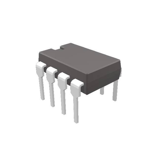


 工商网监
湘ICP备2023018690号
工商网监
湘ICP备2023018690号
