SY7901
High Efficiency 500kHz, 25V PWM Controller
with DC Input Current Limit
General Description
Features
•
•
•
•
•
•
Input Voltage Range 3V to 25V
500kHz Fixed Switching Frequency
An Accurate DC Input Current Limit
External Compensation
Internal Soft-start Limits the Inrush Current
Integrated Low Side Driver: 1.5A Sourcing and 3A
Sinking
• RoHS Compliant and Halogen Free
• Compact Package: DFN3×3-10
The SY7901 is a current mode DC/DC controller
targeted for Boost, Sepic, Flyback and Forward
applications. The SY7901 has an accurate DC input
current limit. External compensation provides flexible
adjustment of control loops for different applications.
The internal low side driver is capable of sourcing 1.5A
and sinking 3A current.
Ordering Information
SY7901 □(□□)□
Applications
Temperature Code
Package Code
Optional Spec Code
l-F
or
VIN
半
Typical Applications
Note
----
芯
Package type
DFN3×3-10
导
小
Ordering Number
SY7901DBC
• GPS Navigation Systems
• Handheld Devices
• Portable Media Player
CIN
COMP
en
tia
R4
C4
Sil
erg
yC
on
fid
ON/OFF
SY7901 Rev. 0.9C
© 2020 Silergy Corp.
CSS
SS
C1
L
IN
C2
VOUT
VCC
EN
GATE
FB
CS
RG
C
M
R1
Co
R3
GND
D
R2
RS
ISEN
C3
Figure1. Schematic Diagram
Silergy Corp. Confidential- Prepared for Customer Use Only
1
All Rights Reserved.
�SY7901
Pinout (top view)
EN
1
10
VIN
SS
2
9
VCC
FB
3
8
GATE
COMP
4
7
CS
SGND
5
6
ISEN
PGND
(DFN3×3-10)
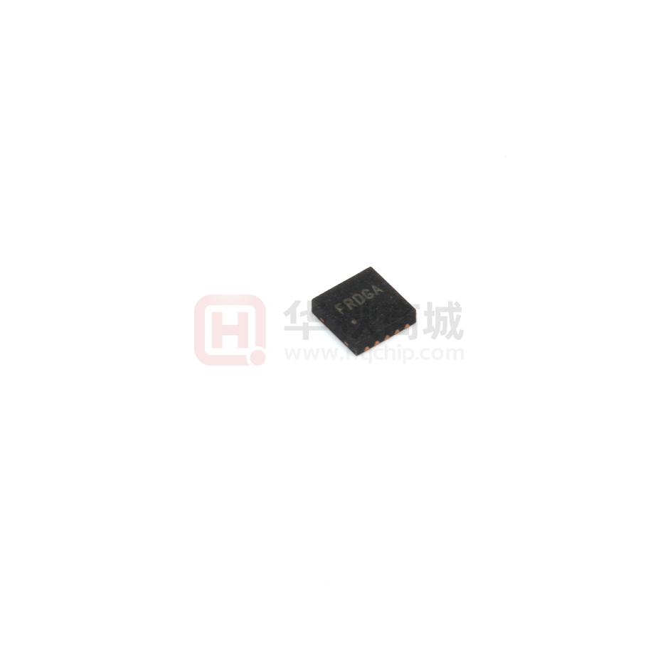
Top Mark: FRxyz for SY7901 (Device code: FR, x=year code, y=week code, z= lot number code)
Pin Number
VIN
10
VCC
9
GATE
8
CS
7
ISEN
6
SGND
5
COMP
4
FB
3
导
小
半
l-F
or
2
1
Exposed Paddle
en
tia
SS
EN
PGND
Pin Description
Input pin. Decouple this pin to the PGND pin with at least a 1µF ceramic
capacitor.
5V Internal LDO output from VIN. Connect a 4.7 µF capacitor from this pin to
PGND.
Driver pin. Connect the gate of the power NFET to this pin.
Current sense pin. Connect an external current sensing resistor RS from this
pin to GND. The voltage on this pin is used for providing MOSFET current
feedback in the control loop and cycle-by-cycle peak current limit. Peak
current limit is triggered when the sensed voltage plus the slope compensation
exceed 340mV.
Connect this pin to CS to program the input average current limit. The input
current limit should be IiLIM=100mV/Rs
Signal ground pin.
External compensation pin. Connect the RC network from this pin to SGND to
compensate the control loop.
Output voltage feedback pin. Connect this pin to the output voltage divider to
program output voltage: VOUT=1V×(1+R1/R2)
Connect a capacitor from this pin to SGND to program the soft-start time.
Enable pin. Pull it high to turn on the chip. Do not leave this pin floating.
Power ground pin.
芯
Pin Name
fid
Absolute Maximum Ratings (Note 1)
Sil
erg
yC
on
IN, EN ----------------------------------------------------------------------------------------------------------------------------- 26V
GATE ------------------------------------------------------------------------------------------------------------------- VCC+0.3V
All Other Pins ---------------------------------------------------------------------------------------------------------------------- 6V
Power Dissipation, P D @ TA = 25°C, DFN3×3-10--------------------------------------------------------------- 2.6W
Package Thermal Resistance (Note 2)
θJA ---------------------------------------------------------------------------------------------------------------------- 38°C/W
θJC ----------------------------------------------------------------------------------------------------------------------- 8°C/W
Junction Temperature Range -------------------------------------------------------------------------------------- -40 to 150°C
Lead Temperature (Soldering, 10 sec.) -------------------------------------------------------------------------- 260°C
Storage Temperature Range ------------------------------------------------------------------------------------- -65°C to 150°C
Recommended Operating Conditions (Note 3)
IN--------------------------------------------------------------------------------------------------------------------- 3V to 25V
Junction Temperature Range ------------------------------------------------------------------------------------ -40°C to 125°C
Ambient Temperature Range ----------------------------------------------------------------------------------- -40°C to 85°C
SY7901 Rev. 0.9C
© 2020 Silergy Corp.
Silergy Corp. Confidential- Prepared for Customer Use Only
2
All Rights Reserved.
�SY7901
Electrical Characteristics
(VIN = 12V, TA = 25°C, unless otherwise specified)
Parameter
Input Voltage Range
Quiescent Current
Shutdown Current
Feedback Reference Voltage
FB Input Current
Current Sense Limit
Internal Slope Compensation
Gm of EA
Gate Driver Output Peak Current
Conditions
VVCC
TSD
THYST
VIN=5.5V
Min
3
FB=1.1V
EN=0
VFB=VIN
0.98
-50
98
Typ
170
0.1
1
100
40
300
1.5
3
Max
25
1.02
50
102
1.5
0.4
2.9
4.9
0.3
500
200
200
5
150
20
5.1
Unit
V
µA
µA
V
nA
mV
mV/µS
µA/V
A
A
V
V
V
V
kHz
ns
ns
V
℃
℃
半
导
小
芯
EN Rising Threshold
EN Falling Threshold
Input UVLO threshold
UVLO hysteresis
Oscillator Frequency
Min ON Time
Min OFF Time
Internal LDO Output
Thermal Shutdown
Thermal Hysteresis
Symbol
VIN
IQ
ISHDN
VREF
IFB
ISEN
VSLOPE
Gm
ISOURCE
ISINK
VENH
VENL
VUVLO
VHYS
FOSC
tia
l-F
or
Note 1: Stresses beyond “Absolute Maximum Ratings” may cause permanent damage to the device. These are for
stress ratings. Functional operation of the device at these or any other conditions beyond those indicated in the
operational sections of the specifications is not implied. Exposure to absolute maximum rating conditions for
extended periods may affect device reliability.
on
fid
en
Note 2: θ JA is measured in the natural convection at TA = 25°C on a low effective single layer thermal conductivity
test board of JEDEC 51-3 thermal measurement standard. Test condition: Device mounted on 2” x 2” FR-4 substrate
PCB, 2oz copper, with minimum recommended pad on top layer and thermal vias to bottom layer ground plane.
Sil
erg
yC
Note 3: The device is not guaranteed to function outside its operating conditions.
SY7901 Rev. 0.9C
© 2020 Silergy Corp.
Silergy Corp. Confidential- Prepared for Customer Use Only
3
All Rights Reserved.
�SY7901
DFN3×3-10 Package Outline
PCB layout (recommended)
Side View
Sil
erg
yC
on
fid
en
tia
l-F
or
半
导
小
芯
Top View
Detail A
Pin1 identifier: two options
Bottom View
Notes: All dimensions are in millimeters and exclude mold flash & metal burr.
SY7901 Rev. 0.9C
© 2020 Silergy Corp.
Silergy Corp. Confidential- Prepared for Customer Use Only
4
All Rights Reserved.
�SY7901
Taping & Reel Specification
1. DFN3×3-10 taping orientation
3.9/4.1
11.7/12.3
1.45/1.55
Feeding direction
Sil
erg
yC
on
fid
en
Reel
Size
tia
l-F
or
半
导
小
芯
2. Carrier Tape & Reel specification for packages
Package
types
DFN3×3
Tape width
(mm)
Pocket
pitch(mm)
Reel size
(Inch)
Trailer
length(mm)
Leader length
(mm)
Qty per
reel
10
8
13"
400
400
5000
SY7901 Rev. 0.9C
© 2020 Silergy Corp.
Powered by TCPDF (www.tcpdf.org)
Silergy Corp. Confidential- Prepared for Customer Use Only
5
All Rights Reserved.
�
很抱歉,暂时无法提供与“SY7901DBC”相匹配的价格&库存,您可以联系我们找货
免费人工找货- 国内价格
- 1+3.11880
- 10+2.84760
- 30+2.79336


 工商网监
湘ICP备2023018690号
工商网监
湘ICP备2023018690号

