山东晶导微电子有限公司
ES2A THRU ES2J
Jingdao Microelectronics
Surface Mount Superfast Recovery Rectifier
Reverse Voltage – 50 to 600 V
PINNING
Forward Current –2 A
PIN
FEATURES
• For surface mounted applications
• Low profile package
• Glass Passivated Chip Junction
• Superfast reverse recovery time
• Lead free in comply with EU RoHS 2011/65/EU directives
DESCRIPTION
1
Cathode
2
Anode
1
2
Top View
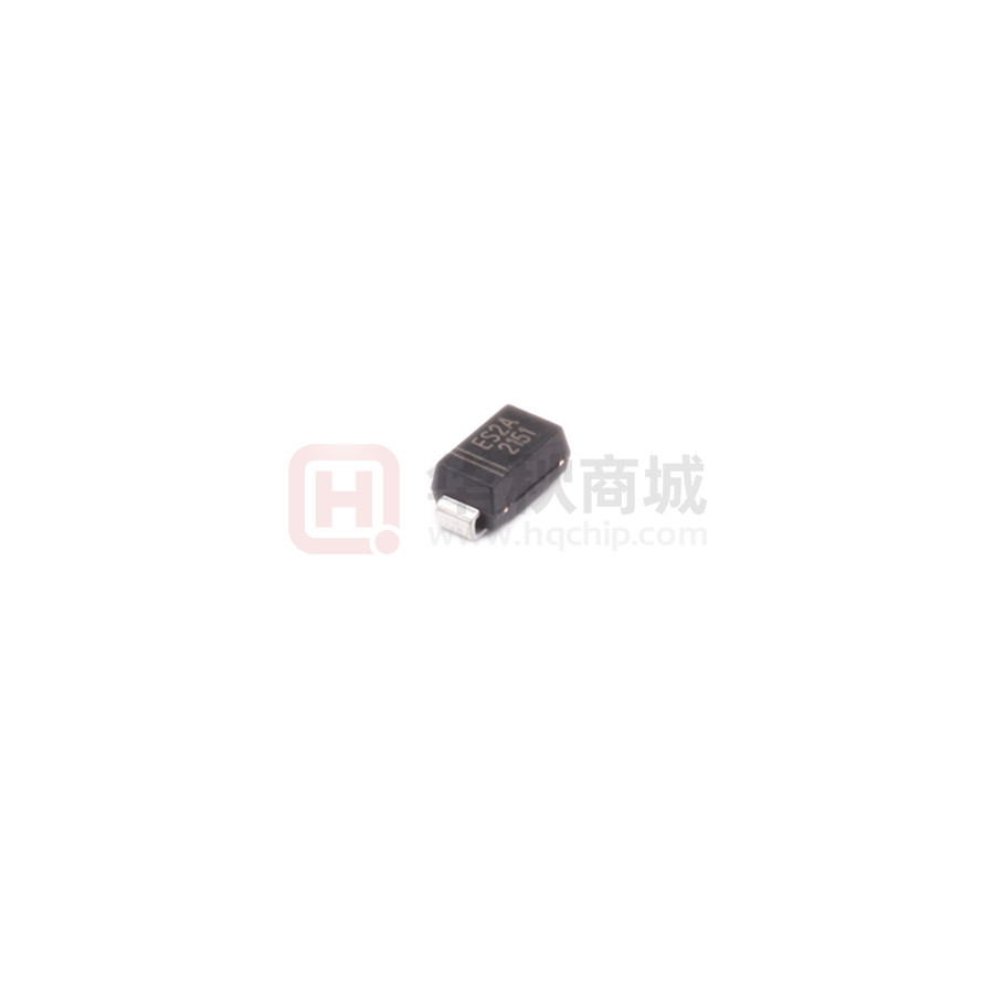
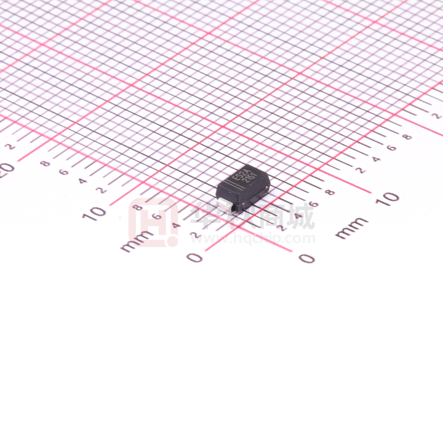
Marking Code: ES2A~ES2J
Simplified outline SMA and symbol
MECHANICAL DATA
• Case: SMA
• Terminals: Solderable per MIL-STD-750, Method 2026
• A pprox. Weight: 0.055g / 0.002oz
Absolute Maximum Ratings and Characteristics
Ratings at 25 °C ambient temperature unless otherwise specified. Single phase, half wave, 60 Hz, resistive or inductive load.
For capacitive load, derate current by 20%.
Symbols
ES2A
ES2B
ES2C
ES2D
ES2E
ES2G
ES2J
Units
Maximum Repetitive Peak Reverse Voltage
V RRM
50
100
150
200
300
400
600
V
Maximum RMS voltage
V RMS
35
70
105
140
210
280
420
V
Maximum DC Blocking Voltage
V DC
50
100
150
200
300
400
600
V
Maximum Average Forward Rectified Current
at T c = 125 °C
I F(AV)
2
A
Peak Forward Surge Current 8.3 ms Single Half
Sine Wave Superimposed on Rated Load
I FSM
50
A
Maximum Forward Voltage at 2 A
VF
Parameter
Maximum DC Reverse Current
T a = 25 °C
at Rated DC Blocking Voltage
T a =125 °C
Typical Junction Capacitance
at V R =4V, f=1MHz
Maximum Reverse Recovery Time
(1)
Typical Thermal Resistance (2)
Operating and Storage Temperature Range
1.25
1
1.68
V
IR
5
100
μA
Cj
40
pF
t rr
35
ns
RθJA
60
°C/W
T j , T stg
-55 ~ +150
°C
(1)Measured with I F = 0.5 A, I R = 1 A, I rr = 0.25 A .
(2)P.C.B. mounted with 1.0 X 1.0" (2.54 X 2.54 cm) copper pad areas.
2015.11
SMA-E-ES2A~ES2J-2A600V
Page 1 of 3
�山东晶导微电子有限公司
ES2A THRU ES2J
Jingdao Microelectronics
Fig.1 Reverse Recovery Time Characteristic And Test Circuit Diagram
50 ohm
Noninductive
t rr
10 ohm
Noninductive
+0.5
D.U.T
+
PULSE
GENERATOR
Note 2
25Vdc
approx
0
-
-0.25
1 ohm
NonInductive
OSCILLOSCOPE
Note 1
-1.0
Note:1.Rise Time = 7ns, max.
Input Impedance = 1megohm,22pF.
2. Ries Time =10ns, max.
Source Impedance = 50 ohms.
10ns/div
Set time Base for 10ns/div
Fig.3 Typical Reverse Characteristics
3.0
300
2.5
I R - Reverse Current ( μ A)
Average Forward Current (A)
Fig.2 Maximum Average Forward Current Rating
2.0
1.5
1.0
0.5
Single phase half-wave 60 Hz
resistive or inductive load
100
T J =125°C
10
T J =75°C
1.0
T J =25°C
0.1
0.0
25
50
75
100
125
150
175
20
0
40
Case Temperature (°C)
80
100
Fig.5 Typical Junction Capacitance
10
Junction Capacitance ( pF)
Instaneous Forward Current (A)
Fig.4 Typical Forward Characteristics
T J =25°C
1.0
ES2A~ES2D
ES2E/WS2G
0.1
60
% of PIV.VOLTS
ES2J
0.01
T J =25°C
100
10
T J=25°C
f = 1.0MHz
V sig = 50mV p-p
1
0.001
0
0.5
1.0
1.5
2.0
2.5
Instaneous Forward Voltage (V)
0.1
1.0
10
100
Reverse Voltage (V)
Peak Forward Surage Current (A)
Fig.6 Maximum Non-Repetitive Peak
Forward Surage Current
60
50
40
30
20
10
8.3 ms Single Half Sine Wave
(JEDEC Method)
00
1
10
100
Number of Cycles
2015.11
www.sdjingdao.com
Page 2 of 3
�山东晶导微电子有限公司
ES2A THRU ES2J
Jingdao Microelectronics
PACKAGE OUTLINE
Plastic surface mounted package; 2 leads
A
A
SMA
c
a
VM
e
A
HE
g
e
E
A
D
E
HE
c
e
g
max
2.2
4.5
2.7
5.2
0.31
1.6
1.5
min
1.9
4.0
2.3
4.7
0.15
1.3
0.9
max
87
181
106
205
12
63
59
min
75
157
91
185
6
51
35
UNIT
mm
mil
g
e
A
D
The recommended mounting pad size
a
0.3
12
Marking
Type number
ES2A
2.4
(94)
mm
Unit :
(mil)
2015.11
ES2A
1.8
(71)
1.8
(71)
1.8
(71)
Marking code
JD511216B0
ES2B
ES2B
ES2C
ES2C
ES2D
ES2D
ES2E
ES2E
ES2G
ES2G
ES2J
ES2J
Page 3 of 3
�
很抱歉,暂时无法提供与“ES2A”相匹配的价格&库存,您可以联系我们找货
免费人工找货- 国内价格
- 1+0.08250
- 100+0.07700
- 300+0.07150
- 500+0.06600
- 2000+0.06325
- 5000+0.06160


 工商网监
湘ICP备2023018690号
工商网监
湘ICP备2023018690号
