ULC0511DN
Features
●
●
●
●
●
Ultra low leakage: nA level
Operating voltage: 5V
Low clamping voltage
Complies with following standards:
– IEC 61000-4-2 (ESD) immunity test
Air discharge: ±15kV
Contact discharge: ±10kV
RoHS Compliant
Dimensions SOD-882
1
2
Pin Configuration
CATHODE
ANODE
Applications
●
●
●
●
●
●
USB 2.0 power and data line
Set-top box and digital TV
Digital video interface (DVI)
Notebook Computers
SIM Ports
10/100 Ethernet
Mechanical Characteristics
●
Package: SOD-882
●
Lead Finish: Lead Free
●
UL Flammability Classification Rating 94V-0
●
Quantity Per Reel:1000pcs
Absolute Maximum Ratings(Tamb=25°C unless otherwise specified)
Parameter
Peak Pulse Power (8/20µs)
ESD per IEC 61000−4−2 (Air)
Symbol
Value
Ppp
Unit
W
±15
VESD
Kv
±10
ESD per IEC 61000−4−2 (Contact)
Operating Temperature Range
TJ
-55 to +125
℃
Storage Temperature Range
TSTJ
-55 to +150
℃
Rev : 01.06.2015
1/4
www.leiditech.com
�ULC0511DN
Electrical Characteristics(TA=25°C unless otherwise specified)
Vc
Part Number
ULC0511DN
Device
Marking
D
VRWM
(V)
VBR
(V)
IT
(mA)
VC
@1A
5
5.4
1
9.8
(Max)
(@A)
IR
μA
(Max)
C
(Pf)
(Typ.)
1
0.5
Characteristic Curves
Figure 1. ESD Clamping Voltage Screenshot
Positive 8 kV Contact per IEC61000−4−2
Rev : 01.06.2015
Figure 2. ESD Clamping Voltage Screenshot
Negative 8 kV Contact per IEC61000−4−2
2/4
www.leiditech.com
�ULC0511DN
IEC61000−4−2 Waveform
IEC 61000−4−2 Spec.
Ipeak
Level
Test
Voltage
(kV)
First Peak
Current
(A)
Current at
30 ns (A)
Current at
60 ns (A)
1
2
7.5
4
2
2
4
15
8
4
3
6
22.5
12
6
4
8
30
16
8
100%
90%
I @ 30 ns
I @ 60 ns
10%
tP = 0.7 ns to 1 ns
Figure 3. IEC61000−4−2 Spec
ESD Gun
Oscilloscope
TVS
50 W
Cable
50 W
Figure 4. Diagram of ESD Test Setup
The following is taken from Application Note
AND8308/D − Interpretation of Datasheet Parameters
for ESD Devices.
ESD Voltage Clamping
For sensitive circuit elements it is important to limit the
voltage that an IC will be exposed to during an ESD event
to as low a voltage as possible. The ESD clamping voltage
is the voltage drop across the ESD protection diode during
an ESD event per the IEC61000−4−2 waveform. Since the
IEC61000−4−2 was written as a pass/fail spec for larger
% OF PEAK PULSE CURRENT
100
PEAK VALUE IRSM @ 8 ms
tr
90
systems such as cell phones or laptop computers it is not
clearly defined in the spec how to specify a clamping voltage
at the device level. ON Semiconductor has developed a way
to examine the entire voltage waveform across the ESD
protection diode over the time domain of an ESD pulse in the
form of an oscilloscope screenshot, which can be found on
the datasheets for all ESD protection diodes. For more
information on how ON Semiconductor creates these
screenshots and how to interpret them please refer to
AND8307/D.
PULSE WIDTH (tP) IS DEFINED
AS THAT POINT WHERE THE
PEAK CURRENT DECAY = 8 ms
80
70
60
HALF VALUE IRSM/2 @ 20 ms
50
40
30
tP
20
10
0
0
20
40
t, TIME (ms)
60
80
Figure 5. 8 X 20 ms Pulse Waveform
Rev : 01.06.2015
3/4
www.leiditech.com
�ULC0511DN
SOD882 Package Outline Drawing
Shanghai Leiditech Electronic Co.,Ltd
Email: sale1@leiditech.com
Tel : +86- 021 50828806
Fax : +86- 021 50477059
Rev : 01.06.2015
4/4
www.leiditech.com
�
很抱歉,暂时无法提供与“ULC0511DN”相匹配的价格&库存,您可以联系我们找货
免费人工找货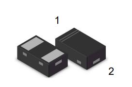


 工商网监
湘ICP备2023018690号
工商网监
湘ICP备2023018690号

