AP2263
Genelal Descliption
Description
nd
uc
to
r
Burst mode control to improve efficiency
and optimize standby power dissipation.
Low startup current and low operating
current.
Voltage clamping at gate output
Soft-start to reduce MOSFET stress
during power on.
Comprehensive protection functions
1 、Under voltage locked with
hysteresis (UVLO) on VDD
2、Over voltage protection (OVP) on
VDD.
co
3、Cycle-by-Cycle current limitation
4 、Current limitation compensation
to obtain the same output current in
universal ac line input
Features
CR
O
Se
mi
AP2263 is highly integrated current mode
PWM control IC optimized for high
performance, low standby power and cost
effective offline flyback converter up to 60W
output power system.
PWM switching frequency is internally
fixed at 65KHz. At no load or light load
condition, the IC operates in ‘burst mode’ to
minimize switching dissipation. Therefore,
lower standby power dissipation and higher
conversion efficiency are achieved.
Due to very small startup current and low
operating current, a big resistor can be used in
the startup circuit to minimize standby power
dissipation.
AP2263 offers comprehensive protection
functions, including Cycle-by-Cycle current
limitation (OCP), over temperature protection
(OTP), Over voltage clamp (OVP)and under
voltage lockout (UVLO) on VDD. The Gate
output is clamped up to 16V to protect the gate
of the power MOSFET.
JS
MI
Digit frequency shuffling technology to
improve EMI performance.
Leading-edge blanking on current sense
input.
Slope compensation.
5 、Over load protection (OLP)
6 、Over temperature protection
(OTP)
300mA drive capability
Applications
Cell Phone Charger
Digital Cameras Charger
Power adaptor
Battery charger
www.jsmsemi.com
第1/12页
�AP2263
JS
MI
CR
O
Se
mi
co
nd
uc
to
r
Application Circuit
www.jsmsemi.com
第2/12页
�AP2263
JS
MI
CR
O
Se
mi
co
nd
uc
to
r
Pin Assignment
www.jsmsemi.com
第3/12页
�AP2263
Ordering Information
Part number
Package
AP2263ST
AP2263S
AP2263D
version number
SOT23-6
SOP-8
DIP-8
Pin Description
Type
Description
GATE
O
Totem-pole gate dive output for the power MOSFET
VDD
P
Chip DC power supply pin
SENSE
I
Current Sense input pin.
FB
I
Feedback input pin.
Gnd
P
Ground.
JS
MI
CR
O
Se
mi
co
nd
uc
to
r
Symbol
www.jsmsemi.com
第4/12页
�AP2263
Se
Absolute Maximum Rating
mi
co
nd
uc
to
r
Block Diagram
Value
Unit
VDD supply voltage
27
V
VDD clamp voltage
29
V
VDD clamp current
10
mA
VFB input voltage
-0.3 to7
V
VSENSE input voltage to SENSE pin
-0.3 to7
V
Min/Max operating junction temperature
-55 to 150
℃
Operating ambient temperature
-20 to 85
℃
JS
MI
CR
O
Parameter
Thermal resistance, Junction to ambient
250
℃/W
Note: Stresses above absolute maximum ratings may cause permanents damage to the device.
Exposure to absolutely maximum-rated conditions for extended periods may affects device
reliability
www.jsmsemi.com
第5/12页
�AP2263
Recommended Operating Conditions
Symbol
Parameter
Min. Max.
Unit
VDD
Supply Voltage Vcc
10 to 26
V
TOA
Operating Ambient Temperature
-20 to 85
℃
ESD-HM
ESD-MM
Human Model
2
150
Electrical Characteristics(TA = 25 ℃, if not otherwise noted)
Parameter
Value
Conditions
Min.
uc
Symbol
VDD operation current
VDD_clamp
lockout enter
VDD under voltage
lockout exit
VDD clamp voltage
3
FB=3V
Se
UVLO(OFF)
VDD under voltage
CR
O
UVLO(ON)
VDD=16V
Idd=10mA
Unit
Typ. Max
co
Idd
VDD=12.5V
mi
VDD start up current
nd
Supply Voltage(V dd Pin)
Idd_startup
to
r
Machine Model
KV
V
15
uA
2.3
mA
7.8
V
13.4
V
32
V
Voltage Feedback (FB Pin)
PWM input gain
JS
MI
AVCS
VFB_open
VFB open loop voltage
IFB_ short
FB pin short current
VFB_ burst
Burst mode voltage
VTH_ PL
TD_PL
DC_ MAX
ΔVFB/ ΔVSENSE
Short FB pin to GND and
measure current
Power limiting FB
threshold voltage
Power limiting delay
time
Maximum duty cycle
VDD=18V, SENSE=0V
FB=3V
www.jsmsemi.com
2
V/V
5.7
V
0.9
mA
1.2
V
3.7
V
120
mS
75
%
第6/12页
�AP2263
Current Sensing (SENSE Pin)
T_blanking
Leading-edge blanking
time
ZSENSE_ IN Input impedance
VTH_ sense
Over current threshold
voltage
250
nS
40
KΩ
0.9
V
Fosc_ BM
Δf_OSC
TA =-20℃ to 100℃
Frequency voltage
VDD=12V to 25V
stability
Burst mode base
frequency
Frequency modulation
range /Base frequency
Gate Drive Output
Output low level
VOH
Output high level
65
VDD=16V, IO=20mA
level
70
Khz
5
%
5
%
20
Khz
-5
VDD=16V, IO=-20mA
output clamp voltage
10
+5
%
0.8
V
V
16
V
Output rising time
VDD=16V, CL=1nF
220
nS
Output falling time
VDD=16V, CL=1nF
70
nS
JS
MI
T_r
T_ f
CR
O
VOL
V_Clamp
nd
stability
uc
Frequency temperature VDD=16V
co
Δf_VDD
60
frequency
mi
Δf_temp
Normal oscillation
Se
Fosc
to
r
Oscillator
www.jsmsemi.com
第7/12页
�AP2263
Application Information
AP2263 is a highly integrated PWM controller IC optimized for offline flyback converter up to 60W
power system. The burst mode control greatly reduces the standby power consumption and helps
the designer easily meet the international energy-saving requirements.
Startup Current and Startup Control
to
r
Startup current ofAP2263 is designed to be very low so that VDD could be charged up above UVLO
threshold level quickly. Therefore, a large value resistor can be used to minimize the power
dissipation in application For AC/DC adaptor within universal input range, a 2 M , 1/2 W resistor
could be connected to VDD capacitor to provide a fast startup and low power dissipation solution.
Operating Current
uc
The Operating current of AP2263 is lower 2.3mA. Therefo e AP2263 can havega ood efficienyc .
Frequency shuffling for EMI improvement
co
nd
The frequency Shuffling is implemented in AP2263The oscillation frequency is modulated with
a random source so that the harmonic energy is spread out. The spread spectrum minimizes
the conduction EMI and therefore reduces system design challenge.
Burst Mode Operation
CR
O
Se
mi
At zero load or light load condition, the main power dissipation in a switching mode power supply
is from switching on the MOSFET, the transformer core and the snubber circuit. The magnitude of
power dissipation is proportional to the number of switching frequency within certain period. Less
switching frequency can reduce the power dissipation.AP2263 adjusts the switching frequency
according to the loading condition. From light load to no load, the FB voltage drops. While the FB
voltage is less than 1.1V, the gate pin output is disabled and kept low, while the FB voltage is
higher than 1.2V, the gate output recovers to normal working mode. This is called “burst mode”. To
reduce audio noise, the switching frequency will be kept higher than 20KHz in burst mode.
Oscillator Operation
JS
MI
The switching frequency is internally fixed at 65kHz. No external frequency setting components
are required on PCB design.
Current Sensing and Leading-Edge Blanking
Cycle-by-Cycle current limitation is offered in AP2263 . The switchin g current is detected by a
resistor into the SENSE pin. An internal leading-edge blanking circuit chops off the SENSE voltage
spike at initial so that the external RC filtering on SENSE pin is no longer required. The current
limiting comparator is disabled and thus cannot turn off the external MOSFET during the blanking
period. PWM duty cycle is determined by the voltage in the SENSE pin and the FB pin.
Internal Synchronized Slope Compensation
Slope compensation circuit adds voltage ramp onto the SENSE voltage according to PWM pulse
width. This greatly improves the close loop stability at CCM and prevents the sub-harmonic
oscillation and thus reduces the output ripple voltage. Slope compensation can help AP2263 obtain
the same output current in universal ac input voltage.
www.jsmsemi.com
第8/12页
�AP2263
GATE DRIVE
GATE pin of AP2263 has 300mA drive current capability and the highest voltage is clamped at 16V.
Therefore, the dissipation of conduction and switching in MOSFET is minimized.
Protection Controls
to
r
AP2263 has comprehensive protection functions including Cycle-by- Cycle current limitation
(OCP), Over Load Protection (OLP) and over voltage clamp, Under Voltage Lockout on VDD
(UVLO), Over Temperature Protection (OTP).
Current limitation compensation
JS
MI
CR
O
Se
mi
co
nd
uc
To obtain the same output current capability, the OLP threshold voltage is compensated for the
different input AC voltage. This function makes the current of OLP is in consistency whatever the
AC input is (110V or 220V).
www.jsmsemi.com
第9/12页
�AP2263
Package Information
JS
MI
CR
O
Se
mi
co
nd
uc
to
r
SOT-23-6
www.jsmsemi.com
第10/12页
�AP2263
JS
MI
CR
O
Se
mi
co
nd
uc
to
r
SOP-8
www.jsmsemi.com
第11/12页
�AP2263
JS
MI
CR
O
Se
mi
co
nd
uc
to
r
DIP 8
www.jsmsemi.com
第12/12页
�
很抱歉,暂时无法提供与“AP2263”相匹配的价格&库存,您可以联系我们找货
免费人工找货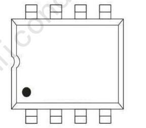


 工商网监
湘ICP备2023018690号
工商网监
湘ICP备2023018690号
