WCM2001
WCM2001
N- and P-Channel Complementary, 20V, Power
MOSFET
VDS (V)
Max. RDS(on) (mΩ)
N-Channel
500@ VGS=4.5V
20
835@ VGS=2.5V
http://www.omnivision-group.com/
ESD Rating:2000V HBM
P-Channel
106@ VGS=-4.5V
-20
155@ VGS=-2.5V
DFN2x2-6L
Descriptions
The
WCM2001
is
the
N-Channel
and
P-Channel
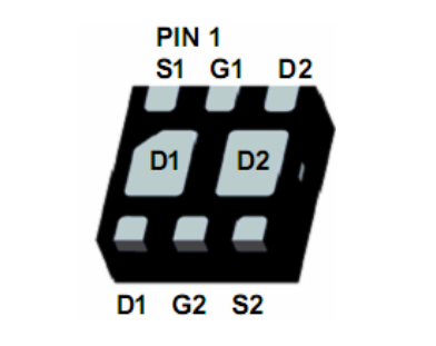
D1
G2
S2
6
5
4
1
S1
2
G1
3
D2
enhancement MOS Field Effect Transistor as a single
package for DC-DC converter or level shift applications,
uses advanced trench technology and design to provide
excellent RDS(ON) with low gate charge. Standard Product
WCM2001 is Pb-free and Halogen-free.
Pin configuration (Top view)
Features
Trench Technology
Supper high density cell design
Excellent ON resistance
Extremely Low Threshold Voltage
Package DFN2x2-6L
WLSI = Company Code
3J = Device Code
WW = Week Code
Marking
Applications
Order information
Driver: Relays, Solenoids, Lamps, Hammers
Power supply converters circuit
Load/Power Switching for portable device
Will Semiconductor Ltd.
1
Device
Package
Shipping
WCM2001-6/TR
DFN2x2-6L
3000/Tape&Reel
May, 2021- Rev.1.4
�WCM2001
Absolute Maximum ratings
Parameter
Symbol
N-Channel
P-Channel
Drain-Source Voltage
VDS
20
-20
Gate-Source Voltage
VGS
±10
±8
1.2
-3.6
A
0.9
-2.9
A
2
-6
A
1.1
2.0
0.7
1.3
Continuous Drain Current
Pulsed Drain Current
Power Dissipation
TA=25°C
TA=70°C
d
ID
IDM
TA=25°C
c
TA=70°C
Operating Junction Temperature
Storage Temperature Range
PD
Unit
V
W
TJ
-55 to 150
°C
TSTG
-55 to 150
°C
Thermal resistance ratings
Single Operation (N-Channel)
Parameter
Symbol
Junction-to-Ambient Thermal Resistance
a
Junction-to-Ambient Thermal Resistance
b
t ≤ 10 s
Steady State
t ≤ 10 s
Steady State
Typical
Maximum
74
113
102
122
156
188
223
268
Typical
Maximum
51
61
77
92
138
165
199
239
RθJA
RθJA
Unit
°C/W
Single Operation (P-Channel)
Parameter
Symbol
Junction-to-Ambient Thermal Resistance
a
Junction-to-Ambient Thermal Resistance
b
t ≤ 10 s
Steady State
t ≤ 10 s
Steady State
RθJA
RθJA
Unit
°C/W
Note:
2
a.
FR-4 board (38mm X 38mm X t1.6mm, 70um Copper) partially covered with copper (645mm area)
b.
FR-4 board (38mm X 38mm X t1.6mm, 70um Copper) minimum pad covered with copper
c.
The power dissipation PD is based on Junction-to-Ambient thermal resistance RθJA t ≤ 10s value and the
TJ(MAX)=150°C.
d.
Repetitive rating, ~10us pulse width, duty cycle ~1%, keep initial TJ =25°C, the maximum allowed junction
temperature of 150°C.
e.
The static characteristics are obtained using ~380us pulses, duty cycle ~1%.
Will Semiconductor Ltd.
2
May, 2021- Rev.1.4
�WCM2001
o
N-Channel Electronics Characteristics (Ta=25 C, unless otherwise noted)
Parameter
Symbol
Test Conditions
Min
Typ
Max
Unit
OFF CHARACTERISTICS
Drain-to-Source Breakdown Voltage
BVDSS
VGS = 0 V, ID = 250uA
Zero Gate Voltage Drain Current
IDSS
VDS =16V, VGS = 0V
Gate-to-source Leakage Current
IGSS
VDS = 0 V, VGS = ±10V
VGS(TH)
VGS = VDS, ID = 250uA
20
V
1
uA
±10
uA
0.7
1.0
V
VGS = 4.5V, ID =800mA
334
500
VGS = 3.1V, ID =600mA
377
660
VGS = 2.5V, ID =300mA
417
835
VGS = 1.8V, ID =200mA
553
1380
ON CHARACTERISTICS
Gate Threshold Voltage
Drain-to-source On-resistance
RDS(on)
0.45
mΩ
CHARGES, CAPACITANCES AND GATE RESISTANCE
Input Capacitance
CISS
Output Capacitance
COSS
Reverse Transfer Capacitance
CRSS
Total Gate Charge
QG(TOT)
Gate-to-Source Charge
QGS
Gate-to-Drain Charge
QGD
VGS = 0 V, f = 1.0MHz,
VDS = 10 V
VGS = 4.5 V, VDS = 10 V,
ID =550mA
29
11
pF
4
0.42
0.1
nC
0.16
SWITCHING CHARACTERISTICS
Turn-On Delay Time
td(ON)
5.9
Rise Time
tr
VGS = 4.5 V, VDS = 10 V,
4.8
Turn-Off Delay Time
td(OFF)
ID=550mA, RG=6Ω
15.5
Fall Time
tf
ns
3.9
BODY DIODE CHARACTERISTICS
Forward Voltage
Will Semiconductor Ltd.
VSD
VGS = 0 V, IS = 800mA
3
0.9
1.2
V
May, 2021- Rev.1.4
�DS
GS
V
-Drain-to-
WCM2001
Source Volta
ge(V)
o
Ice Current
-Drain-to-Sour
(A)
Typical Characteristics (Ta=25 C, unless otherwise noted)
=8V
=6V
V
=5.5V
4
2
0
5
0
15
10
IDS -Drain to Source Current(A)
3.0
VGS=4.5V
2.5
2.0
VGS=3.1V
VGS=2.5V
1.5
1.0
VGS=1.8V
0.5
0.0
0.0
0.2
0.4
0.6
0.8
1.0
1.2
1.4
1.6
1.8
VDS=2V
2.5
Output Characteristics
o
2.0
1.5
o
T=150 C
1.0
0.5
0.0
0.0
2.0
o
T=-50 C
T=25 C
0.5
VDS-Drain-to-Source Voltage(V)
1.0
1.5
2.0
2.5
3.0
3.5
4.0
4.5
VGS -Gate to Source Voltage(V)
d
Transfer Characteristics
d
700
500
RDS(ON)-On Resistance(m)
RDS(ON)-Resistance(m)
ID=800mA
450
400
VGS=3.1V
350
VGS=4.5V
300
600
500
400
300
200
250
0.2
0.4
0.6
0.8
1.0
1.2
1.4
1.6
1.8
1
2.0
2
On-Resistance vs. Drain Current
d
Gate Threshold Voltage Normalized
VGS=4.5V
ID=800mA
1.4
1.2
1.0
0.8
0.6
0.4
-50
-25
0
25
50
75
100
125
150
5
6
7
8
9
10
On-Resistance vs. Junction Temperature
d
1.3
ID=250uA
1.2
1.1
1.0
0.9
0.8
0.7
0.6
0.5
-50
-25
0
25
50
75
100
125
150
Temperature (oC)
Temperature (oC)
Will Semiconductor Ltd.
4
On-Resistance vs. Gate-to-Source Voltage
1.8
1.6
3
VGS-Gate to Source Voltage (V)
IDS-Drain to Source Current(A)
RDS(ON)-On Resistance Normalized
DS
ID-Drain-to-Source Current(A)
3.0
d
Threshold Voltage vs. Temperature
4
May, 2021- Rev.1.4
�WCM2001
50
5
ISD-Source to Drain Current (A)
VGS=0
f=1MHz
C-Capacitance(pF)
40
30
Ciss
20
Coss
Crss
10
0
0
2
4
6
8
4
3
o
T=150 C
2
o
T=25 C
1
10
o
T=-50 C
0.3
0.4
0.5
0.6
0.7
0.8
0.9
1.0
1.1
1.2
1.3
1.4
VSD-Source to Drain Voltage (V)
VDS-Drain to Source Voltage(V)
Capacitance
Body Diode Forward Voltage
d
10
350
O
TJ(Max)=150 C
300
O
TA=25 C
100us
ID-Drain Current (A)
Power(W)
250
200
150
100
1
Limit by Rdson
1ms
10ms
DC
0.1
TJ(MAX)=150 C
1E-5
1E-4
1E-3
0.01
0.1
1
10
100
TA=25 C
DC Pulse
Single
0.01
0.01
1000
1s
10s
o
50
1E-6
100ms
o
0.1
Pulse Width(s)
1
10
100
VDS-Drain to Source Voltage(V)
Single Pulse power
Safe Operating Power
VGS-Gate to Source Voltage (V)
4.5
4.0
VDS=10V
ID=0.55A
3.5
3.0
2.5
2.0
1.5
1.0
0.5
0.0
0.0
0.3
0.6
0.9
1.2
1.5
Gate Charge Characteristics (nC)
Gate Charge Characteristics
Will Semiconductor Ltd.
5
May, 2021- Rev.1.4
�WCM2001
Normalized Effective Transient
Thermal Impedance
10
In Descending Order
D=0.5, 0.3, 0.1, 0.05, 0.02, 0.01, single pluse
1
0.1
single pulse
0.01
1E-3
1E-5
1E-4
1E-3
0.01
0.1
1
10
100
1000
Square Wave Pulse Duration (s)
Transient thermal response (Junction-to-Ambient)
Will Semiconductor Ltd.
6
May, 2021- Rev.1.4
�WCM2001
o
P-Channel Electronics Characteristics (Ta=25 C, unless otherwise noted)
Parameter
Symbol
Test Conditions
Min
Typ
Max
Unit
OFF CHARACTERISTICS
Drain-to-Source Breakdown Voltage
BVDSS
VGS = 0 V, ID = -250uA
-20
V
Zero Gate Voltage Drain Current
IDSS
VDS =-16V, VGS = 0V
-1
uA
Gate-to-source Leakage Current
IGSS
VDS = 0 V, VGS = ±8V
±100
nA
Gate Threshold Voltage
VGS(TH)
VGS = VDS, ID = -250uA
-0.7
-1
V
Drain-to-source On-resistance
RDS(on)
VGS = -4.5V, ID = -2.7A
85
106
VGS = -2.5V, ID = -2.2A
107
155
ON CHARACTERISTICS
-0.45
mΩ
CHARGES, CAPACITANCES AND GATE RESISTANCE
Input Capacitance
CISS
Output Capacitance
COSS
Reverse Transfer Capacitance
CRSS
Total Gate Charge
QG(TOT)
Threshold Gate Charge
QG(TH)
VGS=-4.5 V, VDS =-10 V,
0.4
Gate-to-Source Charge
QGS
ID =-2.3 A
0.8
Gate-to-Drain Charge
QGD
1.4
Turn-On Delay Time
td(ON)
8.5
Rise Time
tr
VGS = -4.5 V, VDS =-6 V,
Turn-Off Delay Time
td(OFF)
ID=-1A, RG=6Ω
Fall Time
tf
VGS = 0 V, f = 1.0MHz,
VDS = -10V
290
64
pF
48
5.9
nC
SWITCHING CHARACTERISTICS
11
ns
34.6
10
BODY DIODE CHARACTERISTICS
Forward Voltage
Will Semiconductor Ltd.
VSD
VGS = 0 V, IS = -1A
7
-0.85
-1.5
V
May, 2021- Rev.1.4
�WCM2001
o
Typical Characteristics (Ta=25 C, unless otherwise noted)
20
20
-IDS -Drain to Source Current(A)
-ID-Drain-to-Source Current(A)
15
VGS=-4V
VGS=-3.1V
10
VGS=-2.5V
5
VGS=-1.8V
0
0.0
0.5
1.0
1.5
VDS=-5V
18
VGS=-4.5V
2.0
2.5
3.0
3.5
4.0
4.5
16
14
12
o
T=150 C
10
8
o
T=25 C
6
4
2
o
T=-50 C
0
0.0
5.0
0.5
1.0
Output Characteristics
1.5
2.0
2.5
3.0
d
Transfer Characteristics
200
d
ID=-2.3A
VGS=-1.8V
RDS(ON)-On Resistance(m)
RDS(ON)-Resistance (m)
4.0
400
180
160
140
VGS=-3.1V
VGS=-2.5V
VGS=-4.5V
120
100
80
60
300
200
100
0
1
2
3
4
5
6
1
2
-IDS-Drain to Source Current(A)
d
5
d
1.2
Gate Threshold Voltage Normalized
VGS=-4.5V
ID=-2.7A
1.3
1.2
1.1
1.0
0.9
0.8
0.7
-50
4
On-Resistance vs. Gate-to-Source Voltage
1.5
1.4
3
-VGS-Gate to Source Voltage (V)
On-Resistance vs. Drain Current
RDSON-On Resistance Normalized
3.5
-VGS -Gate to Source Voltage(V)
-VDS-Drain-to-Source Voltage(V)
-25
0
25
50
75
100
125
0.9
0.8
0.7
0.6
-25
0
25
50
75
100
125
150
o
Temperature ( C)
Temperature ( C)
Will Semiconductor Ltd.
1.0
0.5
-50
150
o
On-Resistance vs. Junction Temperature
ID=-250uA
1.1
d
Threshold Voltage vs. Temperature
8
May, 2021- Rev.1.4
�WCM2001
1
600
V GS=0
-ISD-Source to Drain Current (A)
f=1MHz
C-Capacitance(pF)
500
C iss
400
300
C rss
200
C oss
100
0
0
2
4
6
8
10
12
14
16
18
o
T=150 C
0.1
o
T=25 C
o
T=-50 C
0.01
0.2
20
0.3
-VDS-Drain to Source Voltage(V)
0.4
0.5
0.6
0.7
0.8
0.9
-VSD-Source to Drain Voltage (V)
Capacitance
Body Diode Forward Voltage
d
10
350
O
TJ(Max)=150 C
100us
O
TA=25 C
300
ID-Drain Current (A)
Limit by Rdson
Power(W)
250
200
150
100
1ms
1
10ms
DC
100ms
o
TJ(MAX)=150 C
0.1
1s
o
10s
TA=25 C
DC Pulse
Single
50
1E-5
1E-4
1E-3
0.01
0.1
1
10
100
0.01
0.01
1000
0.1
Pulse Width(s)
1
10
100
VDS-Drain to Source Voltage(V)
Single Pulse power
Safe Operating Power
5
VDS=-10V
-VGS-Gate to Source Voltage (V)
ID=-2.3A
4
3
2
1
0
0
1
2
3
4
5
6
Gate Charge Characteristics (nC)
Gate Charge Characteristics
Will Semiconductor Ltd.
9
May, 2021- Rev.1.4
�WCM2001
Normalized Effective Transient
Thermal Impedance
10
In Descending Order
D=0.5, 0.3, 0.1, 0.05, 0.02, 0.01, single pluse
1
0.1
0.01
1E-3
1E-5
single pulse
1E-4
1E-3
0.01
0.1
1
10
100
1000
Square Wave Pulse Duration (s)
Transient thermal response (Junction-to-Ambient)
Will Semiconductor Ltd.
10
May, 2021- Rev.1.4
�WCM2001
PACKAGE OUTLINE DIMENSIONS
DFN2x2-6L
D
K
II
I
I
E2
1.
H
2.
E
M
D2
e
II
b
E2
1.
D2
2.
L
TOP VIEW
BOTTOM VIEW
0.55
0.55
0.65
0.35
0.35
0.35
0.62
A2
A
A1
0.65
0.62
0.9
SIDE VIEW
0.9
2.4
RECOMMENDED LAND PATTERN(Unit:mm)
Symbol
Dimensions in Millimeters
Min.
Typ.
Max.
A
0.70
0.75
0.80
A1
0.00
-
0.05
A2
0.203 Ref
D
1.90
2.00
2.10
E
1.90
2.00
2.10
D2
0.76
0.93
1.10
E2
0.44
0.60
0.75
b
0.20
0.28
0.35
L
0.17
0.28
0.38
K
0.17
0.27
0.37
H
M
0.2 Ref
0.25
0.35
e
Will Semiconductor Ltd.
0.45
0.65 BSC
11
May, 2021- Rev.1.4
�WCM2001
TAPE AND REEL INFORMATION
RD
Reel Dimensions
Tape Dimensions
W
P1
Quadrant Assignments For PIN1 Orientation In Tape
Q1
Q2
Q1
Q2
Q3
Q4
Q3
Q4
RD
Reel Dimension
W
Overall width of the carrier tape
P1
Pitch between successive cavity centers
Pin1
Pin1 Quadrant
Will Semiconductor Ltd.
User Direction of Feed
7inch
13inch
1 8mm
12mm
16mm
2mm
4mm
8mm
Q1
Q2
Q3
12
Q4
May, 2021- Rev.1.4
�


 工商网监
湘ICP备2023018690号
工商网监
湘ICP备2023018690号
