ESD5641DXX
ESD5641DXX
1-Line, Uni-directional, Transient Voltage Suppressor
http//:www.sh-willsemi.com
Descriptions
The ESD5641DXX is a transient voltage suppressor
3
1 and 2
designed to protect power interfaces. It is suitable to replace
multiple discrete components in portable electronics.
The ESD5641DXX is specifically designed to protect USB
Circuit diagram
port. TVS diode with higher surge capability is used to protect
USB voltage bus pin.
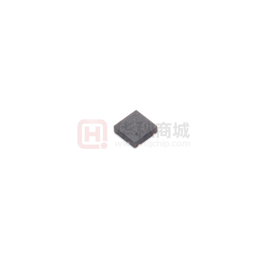
The ESD5641DXX is available in DFN2×2-3L package.
PIN3
Standard products are Pb-free and Halogen-free.
3
Features
Reverse stand-off voltage: 7.5V ~ 15V
Surge protection according to IEC61000-4-5
8/20μs waveform:
IPPM see Table 4
Surge protection according to IEC61643-321
10/1000μs waveform:
IPPM see Table 4
Low clamping voltage
Solid-state silicon technology
1
2
PIN1
PIN2
Pin configuration (Top View)
Applications
Power supply protection
Power management
5641
**YW
Order information
Table 1.
Device
Device
Package
Shipping
ESD5641D07-3/TR
DFN2×2-3L
3000/Tape&Reel
07
ESD5641D10-3/TR
DFN2×2-3L
3000/Tape&Reel
10
ESD5641D12-3/TR
DFN2×2-3L
3000/Tape&Reel
12
5641 = Series code
ESD5641D15-3/TR
DFN2×2-3L
3000/Tape&Reel
15
**
= Device code
YW
= Date code
code
Pin1
Indicator
Marking
Will Semiconductor Ltd.
1
Revision 1.5, 2017/12/11
�ESD5641DXX
Absolute maximum ratings
Table 2.
Parameter
Peak pulse power (tp=8/20μs)
1)3)
Peak pulse power (tp=10/1000μs)
2)3)
ESD according to IEC61000-4-2 air discharge
Symbol
Rating
Unit
PPK
4000
W
PPK
350
W
±30
VESD
ESD according to IEC61000-4-2 contact discharge
Junction temperature
±30
TJ
Operating temperature
TOP
Lead temperature
TL
Storage temperature
TSTG
kV
125
o
-40~85
o
260
o
-55~150
o
C
C
C
C
Notes:
1)
Non-repetitive current pulse, according to IEC61000-4-5.(8/20μs current waveform)
2)
Non-repetitive current pulse, according to IEC61643-321.(10/1000μs current waveform)
3)
Measured from pin 3 to pin 1 and pin 2.
Electrical characteristics (TA = 25oC, unless otherwise noted)
I
IPP
VF
Forward voltage
VRWM Reverse stand-off voltage
IF
Forward current
IR
Reverse leakage current
VFC
Forward clamping voltage
VBR
Reverse breakdown voltage
IPP
Peak pulse current
VCL
Clamping voltage
IPP
Peak pulse current
VFC VF
IBR
IR
VRWM VBR VCL
V
IF
IPP
Definitions of electrical characteristics
Will Semiconductor Ltd.
2
Revision 1.5, 2017/12/11
�ESD5641DXX
o
Electrical characteristics (TA = 25 C, unless otherwise noted)
Table 3.
Reverse
Type number
Standoff
Breakdown voltage
Voltage
VBR(V) IBR = 1mA
Reverse
leakage current
IRM(nA) at VRWM
VRWM (V)
Junction
Forward voltage
capacitance
VF(V) IF = 20mA
F=1MHz,
VR=0V (pF)
Max.
Min.
Typ.
Max.
Typ.
Max.
Min.
Max.
Typ.
Max.
ESD5641D07
7.5
8.0
9.0
10.0
10
1000
0.45
1.25
2200
3000
ESD5641D10
10.0
11.5
13.5
15.5
1
500
0.45
1.25
1500
2000
ESD5641D12
12.0
13.0
15.0
17.0
1
100
0.45
1.25
1200
1800
ESD5641D15
15.0
16.0
17.5
19.0
1
100
0.45
1.25
1000
1500
Table 4.
Rated peak pulse
Clamping voltage
Rated peak pulse
Clamping voltage
current IPP (A)1)3)
VCL(V) at IPP(A)1)3)
current IPP(A)2)3)
VCL(V) at IPP(A)2)3)
Max.
Max.
Max.
Max.
ESD5641D07
190
18
28
13
ESD5641D10
170
23
22
18
ESD5641D12
150
27
16
20
ESD5641D15
130
30
13
25
Type number
Notes:
1)
Non-repetitive current pulse, according to IEC61000-4-5. (8/20μs current waveform)
2)
Non-repetitive current pulse, according to IEC61643-321. (10/1000μs current waveform)
3)
Measured from pin 3 to pin 1 and pin 2.
Will Semiconductor Ltd.
3
Revision 1.5, 2017/12/11
�ESD5641DXX
o
Typical characteristics (TA = 25 C, unless otherwise noted)
Front time: T1= 1.25 T = 8s
Time to half-value: T2= 20s
Peak pulse current (%)
Peak pulse current (%)
100
90
50
T2
10
0
0
20
T
Front time: T1= 1.25 T = 10s
100
90
Time to half-value: T2= 1000s
50
T2
10
0
0
T
Time (s)
T1
8/20μs waveform per IEC61000-4-5
10/1000μs waveform per IEC61643-321
30
30
Pulse waveform:tp=8/20μs
Pulse waveform:tp=10/1000μs
ESD5641D07
ESD5641D10
ESD5641D12
ESD5641D15
Vc-Clamping Voltage (V)
Vc-Clamping Voltage (V)
1000
Time (s)
T1
25
20
15
ESD5641D07
ESD5641D10
ESD5641D12
ESD5641D15
25
20
15
10
10
5
0
50
100
150
5
200
0
5
Ipp-Peak Pulse Current (A)
10
15
20
25
30
Ipp-Peak Pulse Current (A)
Clamping voltage vs. Peak pulse current
Clamping voltage vs. Peak pulse current
Peak pulse power (W)
100
% of Rated power
10000
1000
100
1
10
100
Pulse time (s)
60
40
20
0
1000
0
25
50
75
100
125
150
o
TA - Ambient temperature ( C)
Non-repetitive peak pulse power vs. Pulse time
Will Semiconductor Ltd.
80
Power derating vs. Ambient temperature
4
Revision 1.5, 2017/12/11
�ESD5641DXX
Package outline dimensions
DFN2×2-3L
Symbol
Dimensions In Millimeters
Min.
Typ.
Max.
A
0.50
0.58
0.65
A1
0.00
0.02
0.05
A3
Recommended land pattern (Unit: mm)
0.50
1.30
1.10
1.05
0.40
0.10 REF.
b
0.25
0.30
0.35
D
1.90
2.00
2.10
E
1.90
2.00
2.10
D2
0.95
1.05
1.15
E2
1.40
1.50
1.60
e
1.20
1.30
1.40
H
0.20
0.25
0.30
K
0.20
0.30
0.40
L
0.33
0.39
0.45
R
0.13
-
-
Notes:
This recommended land pattern is for reference
purposes only. Please consult your manufacturing
1.60
Will Semiconductor Ltd.
0.25
0.40
group to ensure your PCB design guidelines are met.
5
Revision 1.5, 2017/12/11
�ESD5641DXX
TAPE AND REEL INFORMATION
RD
Reel Dimensions
Tape Dimensions
W
P1
Quadrant Assignments For PIN1 Orientation In Tape
Q1
Q2
Q1
Q2
Q3
Q4
Q3
Q4
User Direction of Feed
RD
Reel Dimension
7inch
13inch
W
Overall width of the carrier tape
8mm
12mm
P
Pitch between successive cavity centers
2mm
4mm
8mm
Pin1 Quadrant
Q1
Q2
Q3
Pin1
Will Semiconductor Ltd.
6
Q4
Revision 1.5, 2017/12/11
�
很抱歉,暂时无法提供与“ESD5641D15-3/TR”相匹配的价格&库存,您可以联系我们找货
免费人工找货- 国内价格
- 1+0.66980
- 200+0.46140
- 1500+0.41890
- 国内价格
- 5+0.61749
- 20+0.56049
- 100+0.50349
- 500+0.44650
- 1000+0.41990
- 2000+0.40090


 工商网监
湘ICP备2023018690号
工商网监
湘ICP备2023018690号

