LC1486
600mA High PSRR, Fast Response Linear Regulator
DESCRIPTION
FEATURES
LC1486 series is a group of positive voltage
output, low power consumption, low dropout
voltage regulator.
LC1486 can provide output value adjustable from
0.8V to 5.0V.
LC1486 includes high accuracy voltage reference,
error amplifier, current limit circuit and output
driver module with discharge capability.
LC1486 has excellent load and line transient
response and good temperature characteristics,
which can assure the stability of chip and power
system. It uses trimming technique to guarantee
output voltage accuracy within ±2%. And it also
provides foldback short-circuit protection,
thermal protection and output current limit
function.
APPLICATIONS
Power source for cellular phones and various
kind of PCSs
Battery Powered equipment
Power Management of MP3, PDA, DSC,
Mouse, PS2 Games
Reference Voltage Source
Regulation after Switching Power
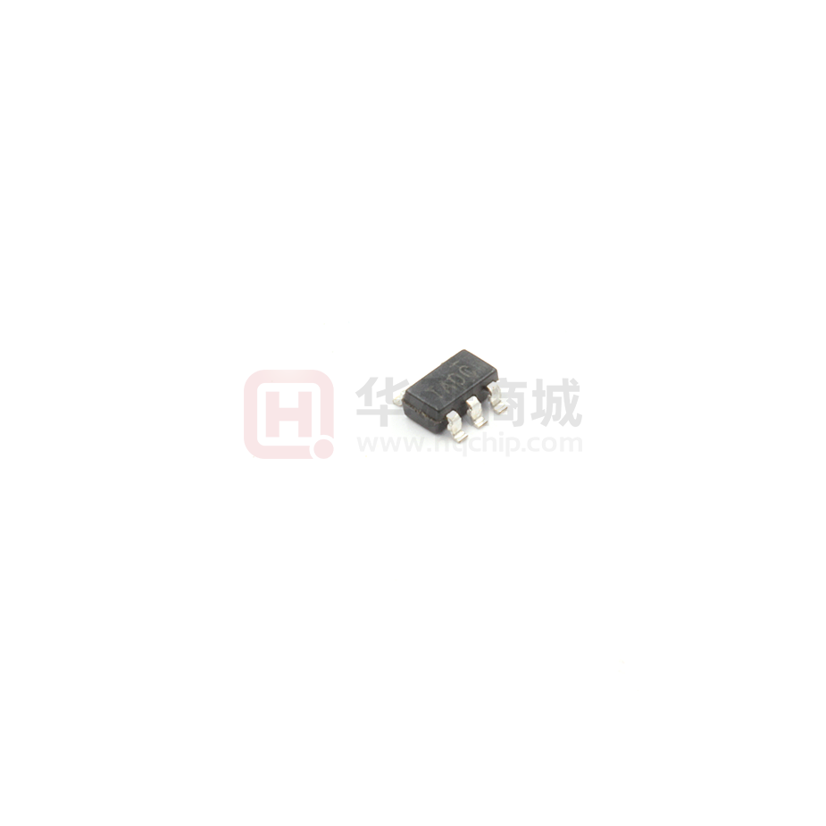
LC1486 is available in SOT23-5 and SC70-5
packages which are lead free.
TYPICAL APPLICATION
VIN
Cin
EN
PIN OUT & MARKING
VOUT
VOUT
VIN
LC1486
GND
On/Off
Low Power Consumption: 40uA (Typ.)
Maximum output current: 600mA
Low dropout Voltage:
170mV@Iout=300mA,Vout=3.3V
355mV@Iout=600mA,Vout=3.3V
Build-in chip enable and discharge circuit
Input voltage range: 2.5~6V
Adjustable Output from 0.8V to 5.0V
Output Voltage Accuracy: ±2%
Ouput current limit: 1A (Typ.)
OCP/SCP/TSD protection
R1
VOUT
FB
5
4
Cout
VOUT
FB
5
4
FB
R2
TAYW
1
Note:
1) Input capacitor (Cin=1uF) and Output capacitor
(Cout=1uF) are recommended in all application circuit.
2) VOUT=VFB*(1+ , VFB=0.8V
VIN
TAYW
2
GND
3
EN
1
2
3
VIN GND EN
SOT23-5
SC70-5
TA: Product Code
YW: Date code (Year & Week)
www.leadchip.com.cn
1
Your final power solution
�LC1486
ORDERING INFORMATION
PART No.
PACKAGE
Tape&Reel
LC1486CB5TR
LC1486CA5TR
SOT23-5
SC70-5
3000/Reel
3000/Reel
ABSOLUTE MAXIMUM RATING
Parameter
Value
Max Input Voltage
Operating Junction Temperature(Tj)
Ambient Temperature(Ta)
SOT23-5
Power Dissipation
SC70-5
Storage Temperature(Ts)
Lead Temperature & Time
8V
150C
-40C –85C
400mW
400mW
-40C -150C
260C,10S
Note: Exceed these limits to damage to the device. Exposure to absolute maximum rating conditions may affect device
reliability.
RECOMMENDED WORK CONDITIONS
Parameter
Value
Input Voltage Range
Ambient Temperature
2.5V to 6V
-40C –85C
ELECTRICAL CHARACTERISTICS
(Test Conditions: CIN=1uF, COUT=1uF, TA=25C, unless otherwise specified. )
Symbol
VIN
VFB
VDROP
Parameter
Input Voltage
Regulated Feedback Voltage
*
Dropout Voltage
Vout
Vin Vout
Vout /
Iout
Conditions
VIN =3.3V, IOUT=10mA
VOUT=1.8V, IOUT =300mA
VOUT =2.5V, IOUT =600mA
VOUT =3.3V, IOUT =600mA
Min
2.5
0.784
Typ
Max
Units
0.8
900
550
355
6
0.816
1350
825
500
V
V
mV
mV
mV
Line Regulation
IOUT =10mA, 2.5V≤VIN≤6V
0.05
0.2
%/V
Load Regulation
VIN =4.3V, VOUT =3.3V
0mA≤IOUT≤600mA
50
80
mV
ISTANDBY
Supply Current
Supply Current (Srandby)
VIN = VOUT +1V
VIN = VOUT +1V, VEN=GND
40
0.1
100
1.0
uA
uA
Vout
T Vout
Output Voltage Temperature
Coefficiency
IOUT =10mA
±100
ppm/C
PSRR
Ripple Rejection
60
dB
ILIM
ISHORT
Current Limit
Short Current Limit
Discharge Resistor
EN Input Voltage “H”
EN Input Voltage “L”
Thermal Shutdown Temp
1
200
280
A
mA
ohm
V
V
°C
IQ
RDISCHARGE
VENH
VENL
TSD
www.leadchip.com.cn
F=1KHz, Ripple=1Vp-p
VIN = VOUT +1V
VIN =4.3V, VOUT =3.3V
VOUT =0V
EN=0, VOUT =3V
1.3
0
Vin
0.35
160
2
Your final power solution
�LC1486
TSH
Thermal Shutdown Hysteresis
30
°C
Note: * VDROP=VIN1-(VOUT2*0.98) VOUT 2 is the output voltage when VIN = VOUT 1+1.0V and IOUT =600mA. VIN 1 is the
input voltage at which the output voltage becomes 98% of Vout1 after gradually decreasing the input voltage.
PIN DESCRIPTION
PIN #
NAME
1
VIN
2
GND
3
EN
4
FB
5
VOUT
DESCRIPTION
Supply Voltage Input. Supply voltage can range from 1.8V to 6V. Bypass with a 1μF capacitor to
GND.
Ground Pin
Enable Pin. This pin has an internal pull-down resistor. A logic low reduces the supply current to
less than 1μA. Connect to IN for normal operation.
Feedback Pin (adjustable voltage version only). This is used to set the output voltage of the
device.
Output Voltage
BLOCK DIAGRAM
EXPLANATION
LC1486 series is a group of positive voltage output, low noise, low power consumption, low dropout
voltage regulator.
LC1486 can provide output value adjustable from 0.8V to 5.0V.
LC1486 includes high accuracy voltage reference, error amplifier, current limit circuit and output driver
module.
LC1486 has excellent load and line transient response and good temperature characteristics, which can
assure the stability of chip and power system. It uses trimming technique to guarantee output voltage
accuracy within±2%. And it also provides fold-back short-circuit protection, thermal protection and output
current limit function.
www.leadchip.com.cn
3
Your final power solution
�LC1486
TYPICAL PERFORMANCE CHARACTERISTICS
Load Regulation
Load Regulation
(Vout=1.8V)
(Vout=3.3V)
2.0
3.6
3.5
Vout (V)
Vout (V)
1.5
1.0
3.4
3.3
3.2
0.5
3.1
Vin=3.3V
Vin=2.8V
0.0
0
200
400
600
Vin=5V
Vin=4.3V
3.0
800
0
100
200
300
Iout (mA)
400
500
600
Iout (mA)
Line Regulation
Line Regulation
(Vout=3.3V)
(Vout=1.8V)
3.354
1.844
3.334
Vout (V)
Vout (V)
1.824
1.804
3.314
3.294
3.274
1.784
3.254
Iout=10mA
Iout=10mA
3.234
1.764
2.5
3.0
3.5
4.0
4.5
5.0
5.5
3.5
6.0
4.0
4.5
5.0
5.5
6.0
Vin (V)
Vin (V)
Dropout Voltage
Dropout Voltage vs. Temp
(Vout=3.3V)
600
450
500
400
350
Dropout (mV)
Dropout (mV)
400
300
200
300
250
200
150
100
100
Vout=3.3V
Vout=2.5V
0
0
100
200
300
400
500
0
0
600
100
200
300
400
500
600
Iout (mA)
Iout (mA)
www.leadchip.com.cn
T=-40°C
T=25°C
T=85°C
50
4
Your final power solution
�LC1486
Iq
Current Limit vs. VIN
(Vout=1.8V)
1,200
60
1,100
1,000
40
Current Limit (mA)
Iq (uA)
50
30
20
T=-40°C
T=25°C
T=85°C
10
0
1
2
3
4
5
900
800
Vout=1.2V
Vout=1.8V
Vout=2.5V
Vout=3.3V
700
600
6
3.5
4.0
4.5
Vin (V)
5.0
5.5
6.0
Vin (V)
EN Chip Enable Response
Vout vs. Temperature
(Orange: Vin; Blue: EN; Green: Vout)
3.5
3.0
Vin, V/div
Vout (V)
2.5
EN, V/div
Vout, V/div
2.0
1.5
1.0
0.5
0.0
-40
0
40
80
120
160
Temperature (C)
Line Transient Response
Load Transient Response
Vout=3.3V, Iout=10mA
Vin=4.3-5.3V, Vout p-p=78mV
(Orange: Vin; Green: Vout)
Vin=4.3V, Vout=3.3V, Iout=10-600mA
Trise=1uS, Tfall=1uS , Vout p-p=74mV
(Pink: Iout; Orange: Vout)
Vin, V/div
Iout, mA/div
Vout, mV/div
www.leadchip.com.cn
Vout, mV/div
5
Your final power solution
�LC1486
PACKAGE OUTLINE
Package
SOT-23-5
Package Dimension:
Package
SC70-5
Devices per reel
3000Pcs
Unit
mm
Devices per reel
3000Pcs
Unit
mm
Package dimension:
www.leadchip.com.cn
6
Your final power solution
�


 工商网监
湘ICP备2023018690号
工商网监
湘ICP备2023018690号
